EP2954835B1 - Module composite opto-électrique, tête de caméra et dispositif d'endoscope - Google Patents
Module composite opto-électrique, tête de caméra et dispositif d'endoscope Download PDFInfo
- Publication number
- EP2954835B1 EP2954835B1 EP14878977.9A EP14878977A EP2954835B1 EP 2954835 B1 EP2954835 B1 EP 2954835B1 EP 14878977 A EP14878977 A EP 14878977A EP 2954835 B1 EP2954835 B1 EP 2954835B1
- Authority
- EP
- European Patent Office
- Prior art keywords
- printed board
- contacts
- area
- composite module
- photoelectric composite
- Prior art date
- Legal status (The legal status is an assumption and is not a legal conclusion. Google has not performed a legal analysis and makes no representation as to the accuracy of the status listed.)
- Not-in-force
Links
Images


Classifications
-
- H—ELECTRICITY
- H04—ELECTRIC COMMUNICATION TECHNIQUE
- H04N—PICTORIAL COMMUNICATION, e.g. TELEVISION
- H04N23/00—Cameras or camera modules comprising electronic image sensors; Control thereof
- H04N23/50—Constructional details
- H04N23/51—Housings
-
- A—HUMAN NECESSITIES
- A61—MEDICAL OR VETERINARY SCIENCE; HYGIENE
- A61B—DIAGNOSIS; SURGERY; IDENTIFICATION
- A61B1/00—Instruments for performing medical examinations of the interior of cavities or tubes of the body by visual or photographical inspection, e.g. endoscopes; Illuminating arrangements therefor
- A61B1/00002—Operational features of endoscopes
- A61B1/00011—Operational features of endoscopes characterised by signal transmission
- A61B1/00013—Operational features of endoscopes characterised by signal transmission using optical means
-
- A—HUMAN NECESSITIES
- A61—MEDICAL OR VETERINARY SCIENCE; HYGIENE
- A61B—DIAGNOSIS; SURGERY; IDENTIFICATION
- A61B1/00—Instruments for performing medical examinations of the interior of cavities or tubes of the body by visual or photographical inspection, e.g. endoscopes; Illuminating arrangements therefor
- A61B1/00002—Operational features of endoscopes
- A61B1/00011—Operational features of endoscopes characterised by signal transmission
- A61B1/00018—Operational features of endoscopes characterised by signal transmission using electrical cables
-
- A—HUMAN NECESSITIES
- A61—MEDICAL OR VETERINARY SCIENCE; HYGIENE
- A61B—DIAGNOSIS; SURGERY; IDENTIFICATION
- A61B1/00—Instruments for performing medical examinations of the interior of cavities or tubes of the body by visual or photographical inspection, e.g. endoscopes; Illuminating arrangements therefor
- A61B1/00002—Operational features of endoscopes
- A61B1/00043—Operational features of endoscopes provided with output arrangements
- A61B1/00045—Display arrangement
-
- A—HUMAN NECESSITIES
- A61—MEDICAL OR VETERINARY SCIENCE; HYGIENE
- A61B—DIAGNOSIS; SURGERY; IDENTIFICATION
- A61B1/00—Instruments for performing medical examinations of the interior of cavities or tubes of the body by visual or photographical inspection, e.g. endoscopes; Illuminating arrangements therefor
- A61B1/00112—Connection or coupling means
- A61B1/00121—Connectors, fasteners and adapters, e.g. on the endoscope handle
- A61B1/00124—Connectors, fasteners and adapters, e.g. on the endoscope handle electrical, e.g. electrical plug-and-socket connection
-
- A—HUMAN NECESSITIES
- A61—MEDICAL OR VETERINARY SCIENCE; HYGIENE
- A61B—DIAGNOSIS; SURGERY; IDENTIFICATION
- A61B1/00—Instruments for performing medical examinations of the interior of cavities or tubes of the body by visual or photographical inspection, e.g. endoscopes; Illuminating arrangements therefor
- A61B1/04—Instruments for performing medical examinations of the interior of cavities or tubes of the body by visual or photographical inspection, e.g. endoscopes; Illuminating arrangements therefor combined with photographic or television appliances
- A61B1/042—Instruments for performing medical examinations of the interior of cavities or tubes of the body by visual or photographical inspection, e.g. endoscopes; Illuminating arrangements therefor combined with photographic or television appliances characterised by a proximal camera, e.g. a CCD camera
-
- A—HUMAN NECESSITIES
- A61—MEDICAL OR VETERINARY SCIENCE; HYGIENE
- A61B—DIAGNOSIS; SURGERY; IDENTIFICATION
- A61B1/00—Instruments for performing medical examinations of the interior of cavities or tubes of the body by visual or photographical inspection, e.g. endoscopes; Illuminating arrangements therefor
- A61B1/04—Instruments for performing medical examinations of the interior of cavities or tubes of the body by visual or photographical inspection, e.g. endoscopes; Illuminating arrangements therefor combined with photographic or television appliances
- A61B1/045—Control thereof
-
- G—PHYSICS
- G02—OPTICS
- G02B—OPTICAL ELEMENTS, SYSTEMS OR APPARATUS
- G02B23/00—Telescopes, e.g. binoculars; Periscopes; Instruments for viewing the inside of hollow bodies; Viewfinders; Optical aiming or sighting devices
- G02B23/24—Instruments or systems for viewing the inside of hollow bodies, e.g. fibrescopes
- G02B23/2476—Non-optical details, e.g. housings, mountings, supports
-
- H—ELECTRICITY
- H04—ELECTRIC COMMUNICATION TECHNIQUE
- H04N—PICTORIAL COMMUNICATION, e.g. TELEVISION
- H04N23/00—Cameras or camera modules comprising electronic image sensors; Control thereof
- H04N23/50—Constructional details
- H04N23/54—Mounting of pick-up tubes, electronic image sensors, deviation or focusing coils
-
- H—ELECTRICITY
- H04—ELECTRIC COMMUNICATION TECHNIQUE
- H04N—PICTORIAL COMMUNICATION, e.g. TELEVISION
- H04N23/00—Cameras or camera modules comprising electronic image sensors; Control thereof
- H04N23/50—Constructional details
- H04N23/555—Constructional details for picking-up images in sites, inaccessible due to their dimensions or hazardous conditions, e.g. endoscopes or borescopes
-
- H—ELECTRICITY
- H04—ELECTRIC COMMUNICATION TECHNIQUE
- H04N—PICTORIAL COMMUNICATION, e.g. TELEVISION
- H04N23/00—Cameras or camera modules comprising electronic image sensors; Control thereof
- H04N23/56—Cameras or camera modules comprising electronic image sensors; Control thereof provided with illuminating means
-
- H—ELECTRICITY
- H04—ELECTRIC COMMUNICATION TECHNIQUE
- H04N—PICTORIAL COMMUNICATION, e.g. TELEVISION
- H04N23/00—Cameras or camera modules comprising electronic image sensors; Control thereof
- H04N23/57—Mechanical or electrical details of cameras or camera modules specially adapted for being embedded in other devices
-
- A—HUMAN NECESSITIES
- A61—MEDICAL OR VETERINARY SCIENCE; HYGIENE
- A61B—DIAGNOSIS; SURGERY; IDENTIFICATION
- A61B1/00—Instruments for performing medical examinations of the interior of cavities or tubes of the body by visual or photographical inspection, e.g. endoscopes; Illuminating arrangements therefor
- A61B1/00064—Constructional details of the endoscope body
- A61B1/00105—Constructional details of the endoscope body characterised by modular construction
-
- H—ELECTRICITY
- H01—ELECTRIC ELEMENTS
- H01R—ELECTRICALLY-CONDUCTIVE CONNECTIONS; STRUCTURAL ASSOCIATIONS OF A PLURALITY OF MUTUALLY-INSULATED ELECTRICAL CONNECTING ELEMENTS; COUPLING DEVICES; CURRENT COLLECTORS
- H01R9/00—Structural associations of a plurality of mutually-insulated electrical connecting elements, e.g. terminal strips or terminal blocks; Terminals or binding posts mounted upon a base or in a case; Bases therefor
- H01R9/03—Connectors arranged to contact a plurality of the conductors of a multiconductor cable, e.g. tapping connections
- H01R9/05—Connectors arranged to contact a plurality of the conductors of a multiconductor cable, e.g. tapping connections for coaxial cables
- H01R9/0515—Connection to a rigid planar substrate, e.g. printed circuit board
Definitions
- the present disclosure relates to a photoelectric composite module, a camera head, and an endoscopic device.
- the endoscopic device according to Patent Literature 1 is an endoscopic device with a detachable head including: an imaging device (hereinafter described also as a camera head) which includes an image sensor; a controller to control the image sensor; and a cable electrically connecting between the imaging device and the controller and configured to transmit various signals therebetween.
- an imaging device hereinafter described also as a camera head
- a controller to control the image sensor
- a cable electrically connecting between the imaging device and the controller and configured to transmit various signals therebetween.
- the endoscopic device employs high-capacity optical transmission in consideration of the fact that image data output by the image sensor contains a large amount of information.
- the camera head includes the image sensor and a printed board electrically connected to the image sensor.
- a photoelectric conversion element converting, into optical signals, imaging signals (electrical signals) output by the image sensor and relayed by the printed board.
- the cable is formed of a composite cable including electrical wires for transmitting electrical signals and an optical wire for transmitting optical signals.
- the electrical wires are electrically connected to the printed board, and transmit, to the printed board (image sensor), control signals and the like (electrical signals) output by the controller.
- the optical wire is connected to the photoelectric conversion element, and transmits, to the controller, optical signals (imaging signals) obtained through conversion by the photoelectric conversion element.
- Patent Literature 1 JP2011-177263A
- US 2013/096380 discloses an endoscope system provided with an optical fiber cable and an electrical cable that transmit pixel information output by a light receiving part.
- the single printed board is provided with two functions: the function of relaying, to the photoelectric conversion element, imaging signals (electrical signals) output by the image sensor; and the function of relaying, to the image sensor, control signals and the like (electrical signals) output by the controller.
- the function of relaying, to the photoelectric conversion element imaging signals (electrical signals) output by the image sensor
- the function of relaying, to the image sensor, control signals and the like electric signals
- the present disclosure is made in view of the above, and an objective thereof is to provide a photoelectric composite module, a camera head, and an endoscopic device which can be downsized.
- the invention is a photoelectric composite module according to claim 1.
- At least part of the first printed board and at least part of the second printed board may be arranged in respective different plain faces.
- At least part of the second printed board may have a curved shape. At least part of the first printed board and at least part of the second printed board may be arranged in respective different faces.
- the second printed board may be formed of a flexible substrate, at least part of which is bendable.
- the first printed board may be formed of a rigid substrate having a planar shape.
- At least part of the first printed board and at least part of the second printed board may be arranged in an overlapping manner.
- the plurality of contacts may include a plurality of first contacts provided in the first area, and a plurality of second contacts provided in the second area.
- the first printed board may be electrically connected to the plurality of first contacts.
- the second printed board may be electrically connected to the plurality of second contacts.
- the first area and the second area may be band-shaped areas being parallel to each other and each extending in a first direction orthogonal to the central axis.
- the first area may be an area including the central axis.
- the first area may be a band-shaped area extending in a first direction orthogonal to the central axis.
- the plurality of first contacts in the first area, may be arranged side by side at a first pitch.
- the plurality of second contacts in the second area, may be arranged side by side at a second pitch, which is smaller than the first pitch.
- the outer frame may have a cylindrical shape.
- the first area may be a band-shaped area including the central axis and extending in a radial direction of the outer frame.
- the first printed board may be arranged along a central axis of the outer frame.
- the second printed board may include a plurality of first lands electrically connected to ground wires constituting a conductor pattern provided to the second printed board, and formed in one of a central area and an other area, which excludes the central area, on a surface of the second printed board in a second direction along the surface, and a plurality of second lands electrically connected to signal wires constituting a conductor pattern provided to the second printed board, and formed in the other of the central area and the other area, which excludes the central area, on the surface of the second printed board.
- the one may be the central area on the surface of the second printed board.
- a plurality of the electrical signal cables each formed of a coaxial cable may be provided.
- Each of the plurality of electrical signal cables may be electrically connected to a corresponding pair of the first land and the second land which is adjacent to the first land.
- the first land and the second land of each of the pairs are formed to be lined up in an inclined direction with respect to the second direction on the surface of the second printed board.
- the first printed board may be electrically connected to a plurality of first contacts arranged side by side in two rows in the interior of the outer frame, the plurality of first contacts being included in the plurality of contacts.
- the plurality of first contacts may include respective first pin-shaped portions being elastically deformable and protruding toward a side where the first printed board and the second printed board are arranged.
- At least one of the plurality of contacts may include a pin-shaped portion protruding toward a side where the first printed board and the second printed board are arranged.
- the second printed board may be formed of a flexible substrate having a first connecting part having a hole through which the pin-shaped portion is inserted, the first connecting part being electrically connected to the at least one of the plurality of contacts, and a second connecting part arranged at a position overlapping with the first printed board when bent with respect to the first connecting part, the second connecting part being electrically connected to the electrical signal cable.
- a camera head is a camera head used in an endoscopic device, and includes: the photoelectric composite module; and an image sensor electrically connected to the first printed board and the second printed board through the first connecting member.
- the camera head may further include: a second connecting member mechanically and electrically connected to the first connecting member; and a casing to which the second connecting member is attached.
- the image sensor is housed in the casing and electrically connected to the first printed board and the second printed board through the first connecting member and the second connecting member.
- An endoscopic device may include the camera head.
- the photoelectric composite module according to the present disclosure includes at least two printed boards: the first printed board configured to act as a relay between the contacts of the first connecting member and the photoelectric conversion element; and the second printed board configured to act as a relay between the contacts of the first connecting member and the electrical signal cable. Accordingly, when the photoelectric composite module according to the present disclosure is used in a camera head, the function of relaying, to the photoelectric conversion element, imaging signals (electrical signals) output by the image sensor is provided to a printed board (first printed board) while the function of relaying, to the image sensor, control signals and the like (electrical signals) output by the controller is provided to another separate printed board (second printed board). Thus, each of the first and second printed boards can be reduced in size as compared to a single printed board provided with these two functions.
- first and second printed boards reduced in size as described above are three-dimensionally arranged, in other words, are not arranged in the same plain face.
- the entire photoelectric composite module can be downsized.
- the camera head according to the present disclosure includes the photoelectric composite module, thus exhibiting advantageous effects similar to those of the photoelectric composite module.
- the endoscopic device includes the camera head, thus exhibiting advantageous effects similar to those of the camera head.
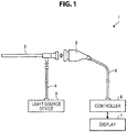
- FIG. 1 shows a schematic configuration of an endoscopic device 1 according to an embodiment of the present disclosure.
- the endoscopic device 1 is an apparatus used in medical fields to observe the interior of an observation object (interior of a living body) such as a human being. Note that, though an endoscopic device using a rigid scope (insertion part 2) as shown in FIG. 1 will be described as the endoscopic device 1 in this embodiment, the endoscopic device 1 is not limited thereto, and may be an endoscopic device using a flexible scope (not shown).
- the endoscopic device 1 includes the insertion part 2, a light source device 3, a light guide 4, a camera head 5, a composite cable 6, a display 7, and a controller 8.
- the insertion part 2 being rigid and having an elongated shape, is inserted into an observation object.
- An optical system for condensing light to form an object image is provided inside the insertion part 2.
- the light source device 3 is connected to one end of the light guide 4, and supplies the one end of the light guide 4 with light to illuminate the interior of the observation object.
- the other end is detachably connected to the insertion part 2.
- the light guide 4 transmits light supplied from the light source device 3 from the one end to the other end, thereby supplying the light to the insertion part 2.
- the light supplied to the insertion part 2 is emitted from the front end of the insertion part 2, and thereby the interior of the observation object is irradiated with the light.
- the light (object image) with which the interior of the observation object is irradiated is condensed by the optical system in the insertion part 2.
- the camera head 5 is detachably connected to the base end of the insertion part 2. Under control of the controller 8, the camera head 5 images the object image formed with light condensed by the insertion part 2, then photoelectrically converts imaging signals (electrical signals) obtained by the imaging into optical signals, and outputs the optical signals.
- the composite cable 6 has a plurality of optical fibers 61 (see FIG. 6 ) and a plurality of electrical signal cables 62 (see FIG. 6 ) inside a jacket 6A (see FIG. 6 ), which is the outermost layer.
- One end of the composite cable 6 is detachably connected to the controller 8 while the other end is detachably connected to the camera head 5.
- the plurality of optical fibers 61 are arranged at a center position of the composite cable 6 in a cross sectional view of the composite cable 6, and used for transmitting optical signals between the camera head 5 and the controller 8.
- the plurality of electrical signal cables 62 are arranged around the plurality of optical fibers 61 in a cross sectional view of the composite cable 6, and used for transmitting electrical signals between the camera head 5 and the controller 8.
- the display 7 displays an image under control of the controller 8.
- the controller 8 acquires optical signals (imaging signals) output from the camera head 5 through the plurality of optical fibers 61, and photoelectrically converts the optical signals to electrical signals. Then, the controller 8 performs predetermined processing on the photoelectrically converted electrical signals, thereby causing the display 7 to display an image imaged by the camera head 5. Meanwhile, the controller 8 outputs control signals and the like (electrical signals) to the camera head 5 through the plurality of electrical signal cables 62.
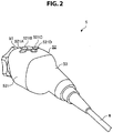
- FIG. 2 is a perspective view, as viewed from the base-end side (side to which the composite cable 6 is connected), of the camera head 5.
- the camera head 5 includes a coupler part 51, an airtight part 52, and a photoelectric composite module 9 (see FIG. 6 ).
- FIG. 2 shows the state in which a cover part 53, having a tubular shape to cover the photoelectric composite module 9 and the base-end side of the airtight part 52, is attached, thus not showing the photoelectric composite module 9.
- the coupler part 51 is used for detachably connecting the camera head 5 to the base end of the insertion part 2, and provided at the front end of the camera head 5.
- FIG. 3 is a perspective view, as viewed from the base-end side (side to which the photoelectric composite module 9 is connected), of the airtight part 52.
- the airtight part 52 includes a casing 521 constituting the exterior of the airtight part 52, a hermetic connector 522 attached to the casing 521, and parts such as a lens unit (not shown), a driving motor (not shown), and an image sensor 523 (see FIG. 4 ) that are housed in the casing 521 in an airtight manner.
- the lens unit forms an object image with light condensed by the insertion part 2 onto an imaging surface of the image sensor 523.
- the lens unit is movable in the optical axis direction.
- the driving motor moves the lens unit along the optical axis when any of switches 521A to 521D ( FIGS. 2 and 3 ), provided to be exposed on the outer surface of the casing 521, is pressed, thereby adjusting a focal distance and a focus of the lens unit.
- the image sensor 523 includes a charge-coupled device (CCD) or a complementary metal-oxide-semiconductor (CMOS) that receives light condensed by the lens unit and converts the received light into electrical signals.
- CCD charge-coupled device
- CMOS complementary metal-oxide-semiconductor
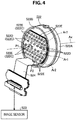
- FIG. 4 is a perspective view, as viewed from the inside of the airtight part 52, of the hermetic connector 522.
- the hermetic connector 522 being a member equivalent to a second connecting member according to the present disclosure, is attached to the base-end side (side to which the photoelectric composite module 9 is connected) of the casing 521 as shown in FIG. 3 .
- This hermetic connector 522 is a round connector and includes a second outer frame 522A, a plate body 522B and a plurality of conductive pins 522C as shown in FIGS. 3 and 4 .
- the second outer frame 522A is made of a metal material and has a cylindrical shape.
- the plate body 522B is made of a metal material and has a disc shape.
- the plate body 522B closes the interior of the second outer frame 522A.
- Each of the plurality of conductive pins 522C has a columnar shape.
- the plurality of conductive pins 522C are attached to the plate body 522B in the state of penetrating the plate body 522B from the front to the back and being insulated from one another.
- first conductive pins 522D the conductive pins 522C provided in a first area Ar1 indicated by the dashed-dotted line in FIG. 4
- second conductive pins 522E the conductive pins 522E provided in two second areas Ar2 indicated by the two-dot chain line
- the first area Ar1 is, in the second outer frame 522A, a band-shaped area including the central axis Ax and extending in a first direction (right-left direction in FIG. 4 ) orthogonal to the central axis Ax.
- the two second areas Ar2 are areas other than the first area Ar1 in the second outer frame 522A, each being a band-shaped area extending in the first direction to be parallel to the first area Ar1.
- the plurality of first conductive pins 522D are arranged in two rows which are side by side in the up-down direction in FIG. 4 .
- the plurality of first conductive pins 522D arranged side by side in the first row which is the upper one, are arranged side by side at a first pitch P1 ( FIG. 4 ).
- the plurality of first conductive pins 522D arranged side by side in the second row which is the lower one, are also arranged side by side at the first pitch P1.
- each first conductive pin 522D in the second row is arranged at a center position, as viewed from above in FIG. 4 , between adjacent first conductive pins 522D arranged side by side in the first row.
- the plurality of second conductive pins 522E are arranged in two rows which are side by side in the up-down direction in FIG. 4 .
- the plurality of second conductive pins 522E arranged side by side in the first row are arranged side by side at a second pitch P2 ( FIG. 4 ), which is smaller than the first pitch P1.
- the plurality of second conductive pins 522E arranged side by side in the first row are also arranged side by side at the second pitch P2.
- each second conductive pin 522E in the second row is arranged at a center position, as viewed from above in FIG. 4 , between adjacent second conductive pins 522E arranged side by side in the first row.
- the plurality of second conductive pins 522E arranged in the upper one of the second areas Ar2 in FIG. 4 are arranged symmetrically to the plurality of second conductive pins 522E arranged in the lower one of the second areas Ar2 with respect to a face passing through the central axis Ax and being parallel to the side-by-side arrangement direction of the second conductive pins 522E.
- an airtight-part side printed board 524 which acts as a relay between (electrically connects) the plurality of conductive pins 522C and the image sensor 523, is attached to the hermetic connector 522 on the inner side of the airtight part 52.
- the airtight-part side printed board 524 relays, to the plurality of first conductive pins 522D, imaging signals (electrical signals) output by the image sensor 523. In addition, the airtight-part side printed board 524 relays, to the image sensor 523, control signals and the like (electrical signals) output by the controller 8 through the composite cable 6, the photoelectric composite module 9, and the plurality of second conductive pins 522E.
- FIG. 5 is a perspective view, as viewed from the front-end side (side to which the airtight part 52 is connected), of the photoelectric composite module 9.
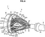
- FIG. 6 is a perspective view, as viewed from the base-end side (side to which the composite cable 6 is connected), of the internal structure of the photoelectric composite module 9.
- FIG. 7 is a side view of the internal structure of the photoelectric composite module 9.
- the photoelectric composite module 9 is mechanically and electrically connected to the hermetic connector 522.
- the photoelectric composite module 9 converts imaging signals (electrical signals) output by the image sensor 523 into optical signals, and then outputs the optical signals to the composite cable 6 (the plurality of optical fibers 61).
- the photoelectric composite module 9 relays, to the hermetic connector 522 (image sensor 523), control signals and the like (electrical signals) output by the controller 8 through the plurality of electrical signal cables 62.
- the photoelectric composite module 9 includes a receptacle 91, a first printed board 92 ( FIGS. 6 and 7 ), two second printed boards 93 ( FIGS. 6 and 7 ) and a covering member 94 ( FIG. 5 ) which has a tubular shape and which covers the base-end side (side opposite to the side to which the hermetic connector 522 is connected) of the receptacle 91.
- FIG. 8 is a perspective view, as viewed from the base-end side, of the receptacle 91.
- the receptacle 91 being a member equivalent to a first connecting member according to the present disclosure, is a round connector mechanically and electrically connected to the hermetic connector 522, and is provided at the front end of the photoelectric composite module 9.
- the receptacle 91 includes a first outer frame 911, an insulator 912, and a plurality of contacts 913.
- the first outer frame 911 is made of a metal material and has a cylindrical shape.
- the insulator 912 is made of an insulating material and closes the interior of the first outer frame 911.
- the insulator 912 there are formed a plurality of insertion holes 912A into which the plurality of conductive pins 522C of the hermetic connector 522 can be inserted when the hermetic connector 522 and the receptacle 91 are connected.
- Each of the plurality of insertion holes 912A is formed in a stepped shape as viewed from the direction along a central axis Ax' of the first outer frame 911 ( FIG. 8 ) in a manner that, in a cross sectional view, the insertion hole 912A has a round shape corresponding to the shape (columnar shape) of the conductive pin 522C at the front-end side (side to which the hermetic connector 522 is connected) of the receptacle 91, and a rectangular shape surrounding this front-end side portion at the base-end side of the receptacle 91.
- the plurality of contacts 913 are respectively provided inside the plurality of insertion holes 912A on the base-end side. Additionally, when the plurality of conductive pins 522C of the hermetic connector 522 are respectively inserted into the plurality of insertion holes 912A, the plurality of contacts 913 are electrically connected to the corresponding plurality of conductive pins 522C.
- FIG. 9 shows an array state of the plurality of contacts 913.
- first contacts 914 the contacts 913 provided in a first area Ar1' indicated by the dashed-dotted line in FIG. 9 will be described as first contacts 914.
- second contacts 915 the contacts 913 provided in two second areas Ar2' indicated by the two-dot chain line in FIG. 9 will be described as second contacts 915.
- the first area Ar1' when viewed from the direction along the central axis Ax' ( FIG. 9 ) of the first outer frame 911, the first area Ar1', facing the first area Ar1 shown in FIG. 4 , is, in the first outer frame 911, a band-shaped area including the central axis Ax' and extending in a first direction (right-left direction in FIG. 9 ) orthogonal to the central axis Ax'.
- the first area Ar1' is a radially extending band-shaped area including the central axis Ax' when viewed from the direction along the central axis Ax'.
- the two second areas Ar2', facing the second areas Ar2 shown in FIG. 4 are areas other than the first area Ar1' in the first outer frame 911, each being a band-shaped area extending in the first direction to be parallel to the first area Ar1'.
- the plurality of first contacts 914 are arranged similarly to the plurality of first conductive pins 522D. In other words, in the first area Ar1', the plurality of first contacts 914 are arranged in two rows which are side by side in the up-down direction in FIG. 9 . In addition, the plurality of first contacts 914 are arranged side by side at the first pitch P1.
- the plurality of second contacts 915 are arranged similarly to the plurality of second conductive pins 522E. In other words, in each of the second areas Ar2', the plurality of second contacts 915 are arranged in two rows which are side by side in the up-down direction in FIG. 9 . In addition, the plurality of second contacts 915 are arranged side by side at the second pitch P2.
- the plurality of first contacts 914 arranged as above have the same shape.
- the shape of one of the first contacts 914 will be described.
- the first contact 914 includes a first main contact body 914A and a first pin-shaped portion 914B.
- the first main contact body 914A provided to the inside of the insertion hole 912A, is formed in a substantially U shape when viewed from the direction along the central axis Ax' so as to extend along the central axis Ax'.
- the inner periphery of the U shape of each first main contact body 914A abuts the outer periphery of the corresponding conductive pin 522C, so that the first main contact body 914A is electrically connected to the conductive pin 522C.
- the first pin-shaped portion 914B protrudes while curving from a base-end portion of the U shape of the first main contact body 914A toward the base-end side (side where the first and second printed boards 92 and 93 are arranged) of the receptacle 91, and is formed in an elastically deformable leaf spring shape.
- the plurality of first contacts 914 arranged side by side in the first row which is the upper one, are provided to the respective insertion holes 912A so that the opening of the U shape of the first main contact body 914A faces upward.
- the plurality of first contacts 914 arranged side by side in the second row which is the lower one, are provided to the respective insertion holes 912A so that the opening of the U shape of the first main contact body 914A faces downward.
- the plurality of second contacts 915 arranged as above have the same shape.
- the shape of one of the second contacts 915 will be described.
- the second contact 915 includes a second main contact body 915A and a second pin-shaped portion 915B.
- the second main contact body 915A is a part having a shape and a function similar to those of the first main contact body 914A.
- the second pin-shaped portion 915B protrudes linearly along the central axis Ax' from a base-end portion of the U shape of the second main contact body 915A toward the base-end side of the receptacle 91.
- the plurality of second contacts 915 arranged in the upper one of the second areas Ar2' are provided to the respective insertion holes 912A so that the opening of the U shape of the second main contact body 915A faces upward.
- the plurality of second contacts 915 arranged in the lower one of the second areas Ar2' are provided to the respective insertion holes 912A so that the opening of the U shape of the second main contact body 915A faces downward.
- the first printed board 92 is formed of a rigid substrate on which a photoelectric conversion element 92A for converting electrical signals into optical signals is mounted.
- the first printed board 92 is electrically connected to the plurality of first contacts 914 of the receptacle 91, and relays, to the photoelectric conversion element 92A, imaging signals (electrical signals) output by the image sensor 523 through the airtight-part side printed board 524, the plurality of first conductive pins 522D, and the plurality of first contacts 914.
- the plurality of optical fibers 61 are connected to the photoelectric conversion element 92A.
- the photoelectric conversion element 92A converts imaging signals (electrical signals) into optical signals, and then outputs the optical signals to the plurality of optical fibers 61.
- the first printed board 92 is arranged along the central axis Ax' on the base-end side of the receptacle 91.
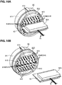
- FIG. 10A is a perspective view, as viewed from the base-end side of the receptacle 91, of a state in which the first printed board 92 is attached to the receptacle 91.
- FIG. 10B is an exploded perspective view showing a state in which the first printed board 92 is detached from the receptacle 91 shown in FIG. 10A .
- the first printed board 92 is attached to the receptacle 91 as described below.
- the first printed board 92 is inserted between the first row, which is the upper one, of the plurality of first contacts 914 (first pin-shaped portions 914B) and the second row, which is the lower one, of the plurality of first contacts 914 (first pin-shaped portions 914B), in FIGS. 10A and 10B .
- the plurality of first pin-shaped portions 914B in the first and second rows hold the first printed board 92 therebetween while being elastically deformed by the pressing of the first printed board 92.
- the plurality of first pin-shaped portions 914B in the first and second rows are electrically connected to lands (not shown) formed on the front and back surfaces of the first printed board 92.
- the first pin-shaped portions 914B are respectively soldered to the lands in the above state, and thereby the first printed board 92 is attached to the receptacle 91.
- the two second printed boards 93 are each formed of a flexible substrate, at least part of which is bendable, and relay, to the plurality of second contacts 915, control signals and the like (electrical signals) output by the controller 8 through the plurality of electrical signal cables 62.
- the control signals and the like (electrical signals) relayed to the plurality of second contacts 915 are output to the image sensor 523 through the plurality of second conductive pins 522E and the airtight-part side printed board 524.
- the second printed board 93 includes a first connecting part 931 ( FIG. 6 ), a second connecting part 932, and an installation part 933 ( FIG. 6 ), installed between the first and second connecting parts 931 and 932.
- the first connecting part 931 has a shape corresponding to one of the second areas Ar2'. Additionally, in the first connecting part 931, there are formed a plurality of holes 931A (refer to FIGS. 6 and 11 ) respectively corresponding to the plurality of second contacts 915 (second pin-shaped portions 915B) arranged in the second area Ar2'.
- the first connecting part 931 is attached to the receptacle 91, by placing the first connecting part 931 on the base-end side end surface of the insulator 912 with the second contacts 915 inserted through the respective holes 931A, and then by soldering the second pin-shaped portions 915B to lands 931B (refer to FIGS. 6 and 11 ) provided on the peripheries of the holes 931A, respectively.
- the second connecting part 932 is arranged at a position overlapping with the first printed board 92 in FIGS. 6 and 7 by bending the installation part 933 with respect to the first connecting part 931 attached to the receptacle 91, as shown in FIGS. 6 and 7 .
- the installation part 933 being part of the second printed board 93, has a curved shape.
- the first connecting part 931 is arranged so as to be substantially orthogonal to the first printed board 92.
- the first connecting part 931 is arranged in a plain face (vertical face orthogonal to the central axis Ax' in FIGS. 6 and 7 ) different from a plain face (horizontal face including the central axis Ax' in FIGS. 6 and 7 ) in which the first printed board 92 is arranged.
- the second connecting part 932 is arranged so as to face the front or back surface of the first printed board 92.
- the second connecting part 932 is also arranged in a plain face different from the plain face in which the first printed board 92 is arranged.
- the installation part 933 has a curved shape and is arranged in a face different from the plain face in which the first printed board 92 is arranged. Accordingly, the first and second printed boards 92 and 93 are three-dimensionally arranged, part of which (the first printed board 92 and the first connecting part 931 or the second connecting part 932) are in different plain faces, part of which (the first printed board 92 and the installation part 933) are in different faces, and part of which (the first printed board 92 and the second connecting part 932) overlap with each other.
- each of the first and second connecting parts 931 and 932 is not limited thereto.
- at least either of the first and second connecting parts 931 and 932 may be formed in a curved shape similarly to the installation part 933.
- plain face means the plain face of the main part of a board (or component member) instead of an absolutely plain face.
- the state in which boards "overlap with each other” means a state in which the boards are lined up in a straight virtual line (vertical line orthogonal to the central axis Ax' in this embodiment) so that the front and back surfaces thereof intersect the virtual line. Accordingly, the state in which boards "overlap with each other” may include the state in which the boards are in contact with each other and the state in which the boards are spaced from each other.
- each second connecting part 932 there are formed a plurality of lands 932A each having a substantially rectangular shape.
- the second connecting part 932 is electrically connected to the plurality of electrical signal cables by soldering the plurality of electrical signal cables 62 to the plurality of lands 932A.
- FIG. 11 shows an array state of the plurality of lands 932A on the second connecting part 932.
- FIG. 11 is a view, as viewed from above (from the direction A in FIG. 6 ), of the receptacle 91 to which only one of the second printed boards 93 (the second printed board 93 arranged at the upper position in FIG. 6 ) is attached.
- first lands 932B the lands 932A provided in a central area ArO indicated by the dashed-dotted line in FIG. 11
- second lands 932C the lands 932A provided in two other areas ArE indicated by the two-dot chain line in FIG. 11
- the central area ArO is an area on the second connecting part 932 positioned at the center in the width direction thereof (right-left direction in FIG. 11 (equivalent to a second direction according to the present disclosure)).
- the two other areas ArE are areas other than the central area ArO on the second connecting part 932.
- the plurality of first lands 932B are arranged side by side in the up-down direction in FIG. 11 in two rows which are side by side in the width direction of the second connecting part 932.
- the plurality of first lands 932B arranged side by side in the first row which is the left one with respect to the center of the second connecting part 932 in the width direction thereof in FIG. 11 , are formed to be inclined downward in FIG. 11 toward the center of the width direction.
- the plurality of first lands 932B arranged side by side in the second row which is the right one with respect to the center in the width direction thereof in FIG. 11 , are formed to be inclined downward in FIG. 11 toward the center of the width direction.
- pairs of the first lands 932B lying side by side in the width direction are arranged symmetrically about the center line connecting the centers in the width direction so as to form a substantially V shape.
- the plurality of first lands 932B are electrically connected respectively to a plurality of ground wires (not shown) constituting a conductor pattern provided to the second printed board.
- the plurality of second lands 932C are arranged side by side in the up-down direction in FIG. 11 in a row.
- the plurality of second lands 932C arranged side by side in the left one of the other areas ArE in FIG. 11 are formed to be each lined up with an adjacent one of the plurality of first lands 932B arranged side by side in the first row, which is the left one in FIG. 11 , in the inclined direction of these first lands 932B, and to be inclined similarly to these first lands 932B.
- the plurality of second lands 932C arranged side by side in the right one of the other areas ArE in FIG. 11 are formed to be each lined up with an adjacent one of the plurality of first lands 932B arranged side by side in the second row, which is the right one in FIG. 11 , in the inclined direction of these first lands 932B, and to be inclined similarly to these first lands 932B.
- the plurality of second lands 932C are electrically connected respectively to a plurality of signal wires (not shown) constituting a conductor pattern provided to the second printed board 93.
- each electrical signal cable 62 is electrically connected to a corresponding pair (the pair enclosed by the broken line in FIG. 11 , for example) of the two of the first land 932B and the second land 932C lined up in either of the inclined directions of the lands 932A.
- FIG. 12 shows a connected state between a pair of the first and second lands 932B and 932C and one of the electrical signal cables 62.
- each of the plurality of electrical signal cables 62 is formed of a coaxial cable.
- each electrical signal cable 62 includes: a core wire 621; an insulation layer 622 covering the outer periphery of the core wire 621; a shield layer 623 covering the outer periphery of the insulation layer 622; and a covering layer 624 covering the outer periphery of the shield layer 623.
- each electrical signal cable 62 is arranged so that a front end portion thereof can be disposed on one of the aforementioned pairs of the first and second lands 932B and 932C so as to extend in the inclined direction thereof from the center of the second connecting part 932 in the width direction thereof.
- the electrical signal cable 62 disposed as above is electrically connected to the second connecting part 932 by soldering the core wire 621 and the shield layer 623 respectively to the second land 932C (signal wire) and the first land 932B (ground wire).
- the photoelectric composite module 9 includes three printed boards: the first printed board 92, which acts as a relay between the first contacts 914 of the receptacle 91 and the photoelectric conversion element 92A; and the two second printed boards 93, which acts as a relay between the second contacts 915 of the receptacle 91 and the electrical signal cables 62. Accordingly, the function of relaying, to the photoelectric conversion element 92A, imaging signals (electrical signals) output by the image sensor 523 is provided to a printed board (the first printed board 92) while the function of relaying, to the image sensor 523, control signals and the like (electrical signals) output by the controller 8 is provided to other separate printed boards (the second printed boards 93). Thus, each of the first and second printed boards 92 and 93 can be reduced in size as compared to a single printed board provided with these two functions.
- first and second printed boards 92 and 93 reduced in size as described above are three-dimensionally arranged, part of which (the first printed board 92 and the first or second connecting parts 931 or 932) are in different plain faces, part of which (the first printed board 92 and each of the installation parts 933) are in different faces, and part of which (the first printed board 92 and the second connecting parts 932) overlap with each other.
- the entire photoelectric composite module 9 can be downsized, and, consequently, the camera head 5 can be downsized.
- the first printed board 92 is formed of a rigid substrate having a planar shape and is arranged along the central axis Ax' on the base-end side of the receptacle 91
- the second printed boards 93 are each formed of a flexible substrate, at least part of which is bendable, and are arranged at positions facing the front and back surfaces of the first printed board 92.
- the first and second printed boards 92 and 93 can be easily set in the aforementioned three-dimensional arrangement.
- the first and second printed boards 92 and 93 can be compactly assembled, and thus the entire photoelectric composite module 9 can be further downsized.
- the plurality of first contacts 914 that relay imaging signals are provided in the first area Ar1' positioned at a center portion of the receptacle 91.
- the first printed board 92 is arranged on the base-end side of the receptacle 91 in a center portion of the receptacle 91 when viewed from the direction along the central axis Ax'.
- first pitch P1 a sufficiently wide pitch between the first contacts 914 can be secured to avoid inter-signal interference, even when differential signals are employed to transmit imaging signals output from the image sensor 523 to the controller 8 at high speed.
- the first printed board 92 is arranged along the central axis Ax' on the base-end side of the receptacle 91.
- the optical fibers 61 can be connected to the photoelectric conversion element 92A mounted on the first printed board 92 without bending the optical fibers 61 arranged at the center of the composite cable 6.
- the plurality of first lands 932B electrically connected to the ground wires are formed in the central area ArO, and the plurality of second lands 932C electrically connected to the signal wires are formed in the other areas ArE.
- the plurality of lands 932A are arranged symmetrically about the center line connecting the centers in the width direction of the second printed board 93 so as to form substantially V shapes.
- the electrical signal cables 62 disposed along the surface of the second printed board 93 can be easily soldered thereto, which can simplify the fitting work.
- each of the plurality of first contacts 914 arranged side by side in upper and lower ( FIG. 10 ) two rows includes the first pin-shaped portion 914B, which is elastically deformable.
- the first printed board 92 can be attached to the receptacle 91 and electrically connected to the first contacts 914, which can simplify the fitting work.
- each of the second printed boards 93 is formed of a flexible substrate.
- the first connecting part 931 constituting the second printed board 93 has the holes 931A through which the second pin-shaped portions 915B of the second contacts 915 are inserted.
- the second printed board 93 when the second printed board 93 are attached to the receptacle 91, soldering can easily be performed with the second pin-shaped portions 915B of the second contacts 915 inserted through the respective holes 931A and with the first connecting part 931 placed on the base-end side end surface of the insulator 912. This can simplify the fitting work.
- the second printed board 93 is formed of a flexible substrate, by simply bending the second printed board 93 after the first connecting part 931 is attached to the receptacle 91 in the aforementioned manner, part (the second connecting part 932) of the second printed board 93 can be arranged at a position overlapping with the first printed board 92.
- the number of the second printed boards 93 is not limited thereto.
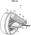
- FIG. 13 shows a modification of the embodiment according to the present disclosure.
- a configuration provided with just one second printed board 93 may be employed.
- a configuration provided with three or more second printed boards 93 may be employed instead.
- the receptacle 91 is employed as the first connecting member according to the present disclosure, but the first connecting member is not limited thereto.
- the hermetic connector 522 may be used as the first connecting member according to the present disclosure.
- a configuration may be employed where the receptacle 91 is omitted, and the first and second printed boards 92 and 93 are connected from outside of the airtight part 52 to the hermetic connector 522 attached to the base-end side of the airtight part 52.
- each of the plurality of conductive pins 522C of the hermetic connector 522 is preferably formed in a shape similar to the first pin-shaped portions 914B of the receptacle 91 (in an elastically deformable leaf spring shape) in consideration of fitting work of the first printed board 92.
- round connectors (the receptacle 91 and the hermetic connector 522) are employed as the first and second connecting members according to the present disclosure, but connectors each having a non-round shape may be employed.
- a first printed board may be arranged at a position other than a center position of each connector (center position when viewed from the direction along the central axis of the connector) as long as a sufficiently wide pitch of a plurality of contacts electrically connected to the first printed board can be secured.
- the pitch (second pitch P2) of the plurality of second contacts 915 is set smaller than the pitch (first pitch P1) of the plurality of first contacts 914, but the pitch length is not limited thereto.
- the pitch of the plurality of second contacts 915 may be configured to be equal to or greater than that of the plurality of first contacts 914.
- first and second printed boards 92 and 93 are three-dimensionally arranged, or in other words are not arranged in the same plain face
- the arrangement of the first and second printed boards 92 and 93 is not limited to that described above, and may be a different arrangement.
- each of the first and second areas Ar1, Ar1', Ar2 and Ar2' may be a non-band-shaped area as long as the areas are independent of one another.
- the endoscopic device 1 may be used not only in medical fields but also in industrial fields, specifically, used as an endoscopic device for observing the interior of an observation object such as a machine structure.
Landscapes
- Health & Medical Sciences (AREA)
- Life Sciences & Earth Sciences (AREA)
- Surgery (AREA)
- Physics & Mathematics (AREA)
- Engineering & Computer Science (AREA)
- Optics & Photonics (AREA)
- Biomedical Technology (AREA)
- Veterinary Medicine (AREA)
- Biophysics (AREA)
- Pathology (AREA)
- Radiology & Medical Imaging (AREA)
- Nuclear Medicine, Radiotherapy & Molecular Imaging (AREA)
- Public Health (AREA)
- Heart & Thoracic Surgery (AREA)
- Medical Informatics (AREA)
- Molecular Biology (AREA)
- Animal Behavior & Ethology (AREA)
- General Health & Medical Sciences (AREA)
- Multimedia (AREA)
- Signal Processing (AREA)
- Astronomy & Astrophysics (AREA)
- General Physics & Mathematics (AREA)
- Endoscopes (AREA)
- Instruments For Viewing The Inside Of Hollow Bodies (AREA)
- Studio Devices (AREA)
Claims (20)
- Module composite photoélectrique (9) comprenant :un câble composite (6) comprenant une pluralité de fibres optiques (61) et une pluralité de fils de signal électrique (62)un premier élément de raccordement ayantun cadre externe (911) ayant une forme tubulaire etune pluralité de contacts électriques (913) disposés dans un intérieur du cadre externe ;un élément de conversion photoélectrique (92A) etune première carte de circuit imprimé (92) sur laquelle l'élément de conversion photoélectrique (92A) est monté, dans lequel l'élément de conversion photoélectrique (92A) est raccordé à la pluralité de fibres optiques et configuré pour convertir un signal électrique en signal optique, la première carte de circuit imprimé (92) étant configurée pour faire office de relais entre les contacts électriques (913) et l'élément de conversion photoélectrique (92A) ; etune seconde carte de circuit imprimé (93) configurée pour faire office de relais entre les contacts électriques (93) et la pluralité de fils de signal électrique (62),dans lequel la première carte de circuit imprimé (92) et la seconde carte de circuit imprimé (93) sont disposées de manière tridimensionnelle, dans lequel au moins une partie de la première carte de circuit imprimé et au moins une partie de la seconde carte de circuit imprimé sont disposées de manière chevauchante.
- Module composite photoélectrique selon la revendication 1,
dans lequel au moins une partie de la première carte de circuit imprimé et au moins une partie de la seconde carte de circuit imprimé sont disposées dans différentes faces simples respectives. - Module composite photoélectrique selon la revendication 1,
dans lequel au moins une partie de la seconde carte de circuit imprimé présente une forme arrondie, et
dans lequel au moins une partie de la première carte de circuit imprimé et au moins une partie de la seconde carte de circuit imprimé sont disposées dans différentes faces respectives. - Module composite photoélectrique selon la revendication 3,
dans lequel la seconde carte de circuit imprimé est formée d'un substrat flexible, dont au moins une partie peut être pliée. - Module composite photoélectrique selon la revendication 3,
dans lequel la première carte de circuit imprimé est formée d'un substrat rigide ayant une forme plane. - Module composite photoélectrique selon la revendication 1,
dans lequel, lorsque l'intérieur du cadre externe est divisé en une première zone et une seconde zone autre que la première zone telle que vue depuis une direction le long d'un axe central du cadre externe, la pluralité de contacts comprennent :une pluralité de premiers contacts disposés dans la première zone etune pluralité de seconds contacts disposés dans la seconde zone,dans lequel la première carte de circuit imprimé est raccordée électriquement à la pluralité de premiers contacts et
dans lequel la seconde carte de circuit imprimé est raccordée électriquement à la pluralité de seconds contacts. - Module composite photoélectrique selon la revendication 6,
dans lequel, à l'intérieur du cadre externe, la première zone et la seconde zone sont des zones en forme de bande qui sont parallèles les unes par rapport aux autres et qui s'étendent chacune dans une première direction orthogonale à l'axe central. - Module composite photoélectrique selon la revendication 6,
dans lequel la première zone est une zone comprenant l'axe central. - Module composite photoélectrique selon la revendication 8,
dans lequel la première zone est une zone en forme de bande s'étendant dans une première direction orthogonale à l'axe central. - Module composite photoélectrique selon la revendication 6,
dans lequel, dans la première zone, la pluralité de premiers contacts sont disposés côte à côte selon un premier pas, et
dans lequel, dans la seconde zone, la pluralité de seconds contacts sont disposés côte à côte selon un second pas, qui est plus petit que le premier pas. - Module composite photoélectrique selon la revendication 10,
dans lequel le cadre externe présente une forme cylindrique et
dans lequel la première zone est une zone en forme de bande comprenant l'axe central et s'étendant dans une direction radiale du cadre externe. - Module composite photoélectrique selon la revendication 1,
dans lequel la première carte de circuit imprimé est disposée le long d'un axe central du cadre externe. - Module composite photoélectrique selon la revendication 1,
dans lequel la seconde carte de circuit imprimé comprendune pluralité de premières pastilles raccordées électriquement à des fils de mise à la terre constituant un motif conducteur disposé sur la seconde carte de circuit imprimé, et formées soit dans une zone centrale, soit dans une autre zone, qui exclut la zone centrale, sur une surface de la seconde carte de circuit imprimé dans une seconde direction le long de la surface etune pluralité de secondes pastilles raccordées électriquement à des fils de signal constituant un motif conducteur disposé sur la seconde carte de circuit imprimé, et formées dans l'autre de la zone centrale et de l'autre zone, qui exclut la zone centrale, sur la surface de la seconde carte de circuit imprimé. - Module composite photoélectrique selon la revendication 13,
dans lequel la zone est la zone centrale sur la surface de la seconde carte de circuit imprimé. - Module composite photoélectrique selon la revendication 14,
dans lequel une pluralité de câbles de signal électrique formés chacun d'un câble coaxial sont prévus,
dans lequel chaque câble de signal électrique de la pluralité de câbles de signal électrique est raccordé électriquement à une paire correspondante de la première pastille et de la seconde pastille qui est adjacente à la première pastille, et
dans lequel la première pastille et la seconde pastille de chacune des paires sont formées pour être alignées dans une direction inclinée par rapport à la seconde direction sur la surface de la seconde carte de circuit imprimé. - Module composite photoélectrique selon la revendication 1,
dans lequel la première carte de circuit imprimé est raccordée électriquement à une pluralité de premiers contacts disposés côte à côte dans deux rangées à l'intérieur du cadre externe, la pluralité de premiers contacts étant inclus dans la pluralité de contacts,
dans lequel la pluralité de premiers contacts comprennent des premières parties respectives en forme de broche qui peuvent être déformées élastiquement et qui font saillie vers un côté où la première carte de circuit imprimé et la seconde carte de circuit imprimé sont disposées, et
dans lequel, lorsque la première carte de circuit imprimé est insérée entre une première rangée des deux rangées des premiers contacts et une seconde rangée des deux rangées des premiers contacts, une pluralité des premières parties en forme de broche supportent la première carte de circuit imprimé tout en étant déformées élastiquement et sont raccordées électriquement à la première carte de circuit imprimé. - Module composite photoélectrique selon la revendication 1,
dans lequel au moins un contact de la pluralité de contacts comprend
une partie en forme de broche faisant saillie vers un côté où la première carte de circuit imprimé et la seconde carte de circuit imprimé sont disposées, et
dans lequel la seconde carte de circuit imprimé est formée d'un substrat flexible ayantune première partie de raccordement ayant un trou à travers lequel la partie en forme de broche est insérée, la première partie de raccordement étant raccordée électriquement au ou aux contacts de la pluralité de contacts, etune seconde partie de raccordement disposée à une position chevauchant la première carte de circuit imprimé lorsqu'elle est pliée par rapport à la première partie de raccordement, la seconde partie de raccordement étant raccordée électriquement au câble de signal électrique. - Tête de caméra utilisée dans un dispositif endoscopique, la tête de caméra comprenant :un module composite photoélectrique selon la revendication 1 ; etun capteur d'image raccordé électriquement à la première carte de circuit imprimé et à la seconde carte de circuit imprimé au moyen du premier élément de raccordement.
- Tête de caméra selon la revendication 18, comprenant en outre :un second élément de raccordement raccordé mécaniquement et électriquement au premier élément de raccordement ; etun boîtier auquel le second élément de raccordement est fixé,dans lequel le capteur d'image est logé dans le boîtier et raccordé électriquement à la première carte de circuit imprimé et à la seconde carte de circuit imprimé au moyen du premier élément de raccordement et du second élément de raccordement.
- Dispositif endoscopique comprenant :
une tête de caméra selon la revendication 18.
Priority Applications (1)
| Application Number | Priority Date | Filing Date | Title |
|---|---|---|---|
| EP15194598.7A EP3020324B1 (fr) | 2014-01-16 | 2014-12-25 | Module composite photoélectrique, tête de caméra et dispositif endoscopique |
Applications Claiming Priority (2)
| Application Number | Priority Date | Filing Date | Title |
|---|---|---|---|
| JP2014006258A JP5806343B2 (ja) | 2014-01-16 | 2014-01-16 | 光電複合モジュール、カメラヘッド、及び内視鏡装置 |
| PCT/JP2014/084326 WO2015107852A1 (fr) | 2014-01-16 | 2014-12-25 | Module composite opto-électrique, tête de caméra et dispositif d'endoscope |
Related Child Applications (2)
| Application Number | Title | Priority Date | Filing Date |
|---|---|---|---|
| EP15194598.7A Division EP3020324B1 (fr) | 2014-01-16 | 2014-12-25 | Module composite photoélectrique, tête de caméra et dispositif endoscopique |
| EP15194598.7A Division-Into EP3020324B1 (fr) | 2014-01-16 | 2014-12-25 | Module composite photoélectrique, tête de caméra et dispositif endoscopique |
Publications (3)
| Publication Number | Publication Date |
|---|---|
| EP2954835A1 EP2954835A1 (fr) | 2015-12-16 |
| EP2954835A4 EP2954835A4 (fr) | 2016-10-19 |
| EP2954835B1 true EP2954835B1 (fr) | 2019-02-06 |
Family
ID=53542753
Family Applications (2)
| Application Number | Title | Priority Date | Filing Date |
|---|---|---|---|
| EP14878977.9A Not-in-force EP2954835B1 (fr) | 2014-01-16 | 2014-12-25 | Module composite opto-électrique, tête de caméra et dispositif d'endoscope |
| EP15194598.7A Active EP3020324B1 (fr) | 2014-01-16 | 2014-12-25 | Module composite photoélectrique, tête de caméra et dispositif endoscopique |
Family Applications After (1)
| Application Number | Title | Priority Date | Filing Date |
|---|---|---|---|
| EP15194598.7A Active EP3020324B1 (fr) | 2014-01-16 | 2014-12-25 | Module composite photoélectrique, tête de caméra et dispositif endoscopique |
Country Status (5)
| Country | Link |
|---|---|
| US (4) | US9810898B2 (fr) |
| EP (2) | EP2954835B1 (fr) |
| JP (1) | JP5806343B2 (fr) |
| CN (1) | CN105025777B (fr) |
| WO (1) | WO2015107852A1 (fr) |
Families Citing this family (34)
| Publication number | Priority date | Publication date | Assignee | Title |
|---|---|---|---|---|
| JP5806343B2 (ja) | 2014-01-16 | 2015-11-10 | ソニー・オリンパスメディカルソリューションズ株式会社 | 光電複合モジュール、カメラヘッド、及び内視鏡装置 |
| JP5840321B1 (ja) * | 2015-08-26 | 2016-01-06 | ソニー・オリンパスメディカルソリューションズ株式会社 | 内視鏡用光電複合ケーブル、内視鏡装置、及び内視鏡システム |
| JP5857150B2 (ja) * | 2015-08-26 | 2016-02-10 | ソニー・オリンパスメディカルソリューションズ株式会社 | カメラヘッド、及び内視鏡システム |
| JP6267678B2 (ja) * | 2015-09-02 | 2018-01-24 | ソニー・オリンパスメディカルソリューションズ株式会社 | 内視鏡システム |
| US11206966B2 (en) | 2016-02-01 | 2021-12-28 | Intuitive Surgical Operations, Inc. | Reduction of endoscope high frequency leakage current using a common-mode choke |
| JP6121078B1 (ja) * | 2016-03-03 | 2017-04-26 | オリンパス株式会社 | 内視鏡システム、内視鏡システムの作動方法 |
| US10575712B2 (en) | 2016-05-20 | 2020-03-03 | Karl Storz Imaging, Inc. | Medical scope device with improved radio frequency data interface |
| US10130241B2 (en) | 2016-05-20 | 2018-11-20 | Karl Storz Imaging, Inc. | Apparatus and method of providing an interface to an electrically powered instrument |
| US10133013B2 (en) | 2016-05-20 | 2018-11-20 | Karl Storz Imaging, Inc. | Apparatus and method of providing an interface to an electrically powered instrument |
| JP6650378B2 (ja) * | 2016-09-08 | 2020-02-19 | 富士フイルム株式会社 | 内視鏡 |
| US10264219B2 (en) | 2016-10-03 | 2019-04-16 | Magna Electronics Inc. | Vehicle camera with compliant coaxial connector |
| JP6858522B2 (ja) | 2016-10-03 | 2021-04-14 | ソニー・オリンパスメディカルソリューションズ株式会社 | 内視鏡装置 |
| JP6464321B2 (ja) * | 2016-12-05 | 2019-02-06 | オリンパス株式会社 | 電子回路ユニット、撮像ユニットおよび内視鏡 |
| US10485629B2 (en) | 2017-02-24 | 2019-11-26 | Sony Olympus Medical Solutions Inc. | Endoscope device |
| JP6873740B2 (ja) | 2017-02-24 | 2021-05-19 | ソニー・オリンパスメディカルソリューションズ株式会社 | 内視鏡装置及びエッジ検出方法 |
| JP6987513B2 (ja) | 2017-03-07 | 2022-01-05 | ソニー・オリンパスメディカルソリューションズ株式会社 | 内視鏡装置 |
| JPWO2018163498A1 (ja) * | 2017-03-08 | 2020-05-14 | ソニー・オリンパスメディカルソリューションズ株式会社 | 医療用装置および医療用装置の製造方法 |
| WO2018173261A1 (fr) | 2017-03-24 | 2018-09-27 | オリンパス株式会社 | Endoscope et module composite photoélectrique |
| JP6996883B2 (ja) | 2017-07-05 | 2022-01-17 | ソニー・オリンパスメディカルソリューションズ株式会社 | 医療用観察装置 |
| JP6996901B2 (ja) | 2017-08-17 | 2022-01-17 | ソニー・オリンパスメディカルソリューションズ株式会社 | 内視鏡システム |
| JP6999369B2 (ja) | 2017-11-02 | 2022-01-18 | ソニー・オリンパスメディカルソリューションズ株式会社 | 内視鏡装置 |
| JP7016681B2 (ja) | 2017-12-01 | 2022-02-07 | ソニー・オリンパスメディカルソリューションズ株式会社 | 内視鏡システム |
| JP6457057B2 (ja) * | 2017-12-06 | 2019-01-23 | ソニー・オリンパスメディカルソリューションズ株式会社 | コネクタ |
| JP7086641B2 (ja) | 2018-02-28 | 2022-06-20 | ソニー・オリンパスメディカルソリューションズ株式会社 | カメラヘッド及び内視鏡 |
| JP2019162371A (ja) | 2018-03-20 | 2019-09-26 | ソニー・オリンパスメディカルソリューションズ株式会社 | 医療用撮像装置及び内視鏡装置 |
| JP2020010757A (ja) | 2018-07-13 | 2020-01-23 | ソニー・オリンパスメディカルソリューションズ株式会社 | 医療用画像処理装置及び医療用観察システム |
| JP2020141761A (ja) | 2019-03-04 | 2020-09-10 | ソニー・オリンパスメディカルソリューションズ株式会社 | 内視鏡用カメラヘッド |
| DE102019003840A1 (de) * | 2019-06-03 | 2020-12-03 | Karl Storz Se & Co. Kg | Videoendoskop und Verfahren zum Konfigurieren eines Videoendoskops |
| US11945144B2 (en) * | 2019-09-06 | 2024-04-02 | Ambu A/S | Tip part assembly for an endoscope |
| DE102020107492A1 (de) | 2020-03-18 | 2021-09-23 | Olympus Winter & Ibe Gmbh | Steckverbindung für ein Videoendoskop, Videoendoskop und Verfahren zur Herstellung einer Steckverbindung |
| WO2022264337A1 (fr) * | 2021-06-16 | 2022-12-22 | オリンパス株式会社 | Unité d'imagerie et endoscope |
| JP7746192B2 (ja) | 2022-03-03 | 2025-09-30 | ソニー・オリンパスメディカルソリューションズ株式会社 | 医療用制御装置及び医療用観察システム |
| CN115341343B (zh) * | 2022-08-05 | 2024-02-13 | 佛山市科华智缝设备有限公司 | 一种上下独立控制的无梭锁边机头 |
| CN115153389B (zh) * | 2022-08-11 | 2025-12-09 | 杭州海康威视数字技术股份有限公司 | 复合线束和内窥镜 |
Family Cites Families (81)
| Publication number | Priority date | Publication date | Assignee | Title |
|---|---|---|---|---|
| US4677471A (en) * | 1985-08-16 | 1987-06-30 | Olympus Optical Co., Ltd. | Endoscope |
| JPS6365840A (ja) * | 1986-04-04 | 1988-03-24 | オリンパス光学工業株式会社 | 内視鏡 |
| US4832003A (en) * | 1986-09-12 | 1989-05-23 | Olympus Optical Co., Ltd. | Electronic endoscope tip |
| US4993405A (en) * | 1989-05-15 | 1991-02-19 | Olympus Optical Co., Ltd. | Imaging apparatus |
| US5868664A (en) * | 1996-02-23 | 1999-02-09 | Envision Medical Corporation | Electrically isolated sterilizable endoscopic video camera head |
| US5754313A (en) * | 1996-07-17 | 1998-05-19 | Welch Allyn, Inc. | Imager assembly |
| JPH10258034A (ja) * | 1997-03-19 | 1998-09-29 | Olympus Optical Co Ltd | 内視鏡用撮像装置 |
| US6080101A (en) * | 1998-08-26 | 2000-06-27 | Olympus Optical Co. Ltd. | Endoscope video camera head which can be autoclaved |
| DE19924189C2 (de) * | 1999-05-27 | 2001-04-26 | Storz Karl Gmbh & Co Kg | Bildaufnehmermodul sowie Verfahren zum Zusammenbauen eines derartigen Bildaufnehmermoduls |
| US6796939B1 (en) * | 1999-08-26 | 2004-09-28 | Olympus Corporation | Electronic endoscope |
| DE19947811C2 (de) * | 1999-10-05 | 2002-06-20 | Winter & Ibe Olympus | Endoskop mit elektrischer Einrichtung und Lichtleiter |
| DE10084189T1 (de) * | 1999-12-09 | 2002-03-07 | Olympus Optical Co | Abbildungseinheit für Endoskope |
| JP2001177263A (ja) * | 1999-12-21 | 2001-06-29 | Hitachi Kokusai Electric Inc | 電子機器のシャーシおよびそのシャーシのガスケット |
| JP2001258835A (ja) * | 2000-03-16 | 2001-09-25 | Olympus Optical Co Ltd | 医療用装置 |
| US6635865B1 (en) * | 2000-07-25 | 2003-10-21 | Andrew J. Soltyk | Imaging sensor microassembly having dual circuit board formed of unsymmetrical T shape |
| US6386913B1 (en) * | 2000-08-14 | 2002-05-14 | Fci Usa, Inc. | Electrical connector for micro co-axial conductors |
| JP3659882B2 (ja) * | 2000-10-31 | 2005-06-15 | オリンパス株式会社 | 内視鏡用撮像装置 |
| DE10121450A1 (de) * | 2001-04-27 | 2002-11-21 | Storz Endoskop Gmbh Schaffhaus | Optisches Instrument, insbesondere Endoskop, mit Wechselkopf |
| ATE546086T1 (de) * | 2001-06-18 | 2012-03-15 | Given Imaging Ltd | In-vivo-sensorvorrichtung mit einer leiterplatte aus starren und flexiblen abschnitten |
| KR100593777B1 (ko) * | 2001-12-07 | 2006-06-30 | 올림푸스 가부시키가이샤 | 의료 기기용 고압 증기 멸균 장치와 멸균 방법 |
| JP2004167083A (ja) | 2002-11-21 | 2004-06-17 | Olympus Corp | 内視鏡装置 |
| JP3668480B2 (ja) * | 2003-03-06 | 2005-07-06 | オリンパス株式会社 | 撮像装置 |
| US7306580B2 (en) * | 2003-04-16 | 2007-12-11 | Cook Incorporated | Medical device with therapeutic agents |
| JP2005066129A (ja) * | 2003-08-26 | 2005-03-17 | Olympus Corp | 電子内視鏡装置 |
| JP4418202B2 (ja) * | 2003-10-06 | 2010-02-17 | オリンパス株式会社 | 内視鏡 |
| US7762950B2 (en) * | 2004-03-25 | 2010-07-27 | Olympus Corporation | Endoscope |
| IL162251A0 (en) * | 2004-05-31 | 2005-11-20 | Medigus Ltd | A reusable laparoscopic or endoscopic camera head |
| JP2015060097A (ja) * | 2013-09-19 | 2015-03-30 | ソニー株式会社 | 光伝送モジュール |
| JP4917436B2 (ja) * | 2004-10-25 | 2012-04-18 | オリンパス株式会社 | 内視鏡装置 |
| JP2006171398A (ja) * | 2004-12-16 | 2006-06-29 | Hitachi Cable Ltd | 光伝送モジュール |
| US8182422B2 (en) * | 2005-12-13 | 2012-05-22 | Avantis Medical Systems, Inc. | Endoscope having detachable imaging device and method of using |
| EP2407084B1 (fr) * | 2005-01-17 | 2017-09-27 | Olympus Corporation | Connecteur electrique pour endoscope |
| AU2006209044A1 (en) * | 2005-01-27 | 2006-08-03 | Super Dimension Ltd. | Endoscope with miniature imaging arrangement |
| JP4987257B2 (ja) * | 2005-06-29 | 2012-07-25 | オリンパス株式会社 | 内視鏡 |
| US7641610B2 (en) * | 2005-08-09 | 2010-01-05 | Olympus Medical Systems Corporation | Endoscope electric connection device |
| JP2007244747A (ja) | 2006-03-17 | 2007-09-27 | Olympus Medical Systems Corp | 撮像装置とこの撮像装置の組立方法 |
| EP1836945A2 (fr) * | 2006-03-20 | 2007-09-26 | Olympus Medical Systems Corp. | Mécanisme à commutation à utiliser dans des appareils médicaux, et dispositif de capture d'images à utiliser dans des endoscopes |
| JP2007260066A (ja) | 2006-03-28 | 2007-10-11 | Pentax Corp | 内視鏡装置 |
| US20070286231A1 (en) * | 2006-05-29 | 2007-12-13 | Pentax Corporation | Optical signal transmitting and receiving apparatus |
| TWI323958B (en) * | 2006-07-14 | 2010-04-21 | Japan Aviation Electron | Electrical component with contact terminal portions arranged in generally trapezoidal shape |
| US7967745B2 (en) * | 2006-09-28 | 2011-06-28 | Given Imaging, Ltd. | In vivo imaging device and method of manufacture thereof |
| US7976459B2 (en) * | 2006-10-17 | 2011-07-12 | Intra L.L.C. | Portable endoscope for intubation |
| US8556807B2 (en) * | 2006-12-21 | 2013-10-15 | Intuitive Surgical Operations, Inc. | Hermetically sealed distal sensor endoscope |
| JP4682158B2 (ja) * | 2007-01-16 | 2011-05-11 | オリンパスメディカルシステムズ株式会社 | 撮像装置 |
| JPWO2008096716A1 (ja) * | 2007-02-05 | 2010-05-20 | 日本電信電話株式会社 | 半導体サブモジュール、コネクタと半導体サブモジュールとの接続方法、および、光モジュール |
| JP5384808B2 (ja) * | 2007-07-02 | 2014-01-08 | オリンパス株式会社 | 内視鏡 |
| JP2009082503A (ja) * | 2007-09-28 | 2009-04-23 | Fujifilm Corp | 撮像装置及びその撮像装置を備えた内視鏡 |
| JP5374861B2 (ja) * | 2007-11-09 | 2013-12-25 | オムロンヘルスケア株式会社 | 血中成分濃度測定装置および血中成分濃度測定装置の制御方法 |
| JP4987790B2 (ja) * | 2008-04-15 | 2012-07-25 | オリンパスメディカルシステムズ株式会社 | 撮像装置 |
| JP2010005148A (ja) | 2008-06-27 | 2010-01-14 | Fujinon Corp | 内視鏡及び内視鏡の信号伝送方法 |
| JP5392533B2 (ja) * | 2008-10-10 | 2014-01-22 | ソニー株式会社 | 固体撮像素子、光学装置、信号処理装置及び信号処理システム |
| US8314835B2 (en) * | 2009-01-23 | 2012-11-20 | Olympus Corporation | Endoscope adapter including light emitting diode, and adapter type endoscope |
| WO2011030608A1 (fr) * | 2009-09-11 | 2011-03-17 | オリンパスメディカルシステムズ株式会社 | Dispositif de prise d'image et procédé de fabrication de dispositif de prise d'image |
| EP2478825B1 (fr) * | 2009-10-28 | 2015-08-26 | Olympus Medical Systems Corp. | Connecteur pour appareil médical |
| JP5493744B2 (ja) * | 2009-11-12 | 2014-05-14 | 富士通株式会社 | 光電気混載基板、および、光電気混載基板の製造方法 |
| JP5080695B2 (ja) * | 2010-02-01 | 2012-11-21 | オリンパスメディカルシステムズ株式会社 | 内視鏡用撮像ユニット |
| JP5452282B2 (ja) * | 2010-02-26 | 2014-03-26 | オリンパス株式会社 | 固体撮像装置 |
| JP2011177263A (ja) | 2010-02-26 | 2011-09-15 | Olympus Corp | 内視鏡 |
| WO2011114957A1 (fr) * | 2010-03-16 | 2011-09-22 | オリンパスメディカルシステムズ株式会社 | Système connecteur |
| JP2011212161A (ja) * | 2010-03-31 | 2011-10-27 | Fujifilm Corp | 固体撮像装置及び内視鏡装置 |
| CN102240203A (zh) * | 2010-05-12 | 2011-11-16 | 无锡市华焯光电科技有限公司 | 超柔性光电复合带状线内窥镜 |
| JP5704878B2 (ja) * | 2010-09-30 | 2015-04-22 | オリンパス株式会社 | 光電気変換コネクタ、光伝送モジュール、撮像装置および内視鏡 |
| WO2012046856A1 (fr) * | 2010-10-08 | 2012-04-12 | オリンパスメディカルシステムズ株式会社 | Dispositif d'imagerie |
| JP5436470B2 (ja) * | 2011-01-31 | 2014-03-05 | 富士フイルム株式会社 | 撮像装置及びこれを備えた電子内視鏡 |
| US9341791B2 (en) * | 2011-04-07 | 2016-05-17 | Sony Corporation | Optical module, manufacturing method of optical module and optical communication device |
| US9380928B2 (en) * | 2011-06-06 | 2016-07-05 | Fujikura Ltd. | Structure of imaging part in electronic visualized catheter |
| DE102011106386A1 (de) * | 2011-07-04 | 2013-01-10 | Karl Storz Gmbh & Co. Kg | Endoskopische Anordnung |
| WO2013084548A1 (fr) * | 2011-12-07 | 2013-06-13 | オリンパスメディカルシステムズ株式会社 | Endoscope électronique |
| JP5926955B2 (ja) * | 2011-12-28 | 2016-05-25 | オリンパス株式会社 | 撮像機構及び内視鏡装置 |
| DE102012202133B4 (de) * | 2012-02-13 | 2022-02-17 | Olympus Winter & Ibe Gmbh | Elektrisches Verbindungsstück für ein Videoendoskop, Videoendoskop und Verfahren zum Herstellen einer elektrischen Verbindung in einem Videoendoskop |
| JP5259852B1 (ja) * | 2012-03-30 | 2013-08-07 | 株式会社東芝 | 支持台、撮像装置、撮像装置の接続方法 |
| DE102012208358A1 (de) * | 2012-05-18 | 2013-11-21 | Olympus Winter & Ibe Gmbh | Videoendoskop |
| JP2013078591A (ja) | 2012-11-21 | 2013-05-02 | Toshiba Corp | 撮像装置、撮像装置の作動方法及び内視鏡装置 |
| WO2014083959A1 (fr) * | 2012-11-29 | 2014-06-05 | オリンパスメディカルシステムズ株式会社 | Structure de connexion pour cartes de circuits |
| JP6300442B2 (ja) * | 2013-01-18 | 2018-03-28 | オリンパス株式会社 | 光伝送モジュールおよび撮像装置 |
| US10025088B2 (en) * | 2013-02-15 | 2018-07-17 | Richard Wolf Gmbh | Assembly for a video endoscope |
| JP5748790B2 (ja) * | 2013-02-27 | 2015-07-15 | 富士フイルム株式会社 | 電子内視鏡、及び電子内視鏡の製造方法 |
| WO2015019669A1 (fr) * | 2013-08-05 | 2015-02-12 | オリンパスメディカルシステムズ株式会社 | Unité d'imagerie pour endoscope |
| JP6411088B2 (ja) * | 2013-09-26 | 2018-10-24 | オリンパス株式会社 | 光伝送モジュールおよび内視鏡 |
| WO2015050044A1 (fr) * | 2013-10-04 | 2015-04-09 | オリンパスメディカルシステムズ株式会社 | Unité de collecte d'image pour endoscope |
| JP5806343B2 (ja) | 2014-01-16 | 2015-11-10 | ソニー・オリンパスメディカルソリューションズ株式会社 | 光電複合モジュール、カメラヘッド、及び内視鏡装置 |
-
2014
- 2014-01-16 JP JP2014006258A patent/JP5806343B2/ja active Active
- 2014-12-25 CN CN201480013450.2A patent/CN105025777B/zh active Active
- 2014-12-25 EP EP14878977.9A patent/EP2954835B1/fr not_active Not-in-force
- 2014-12-25 EP EP15194598.7A patent/EP3020324B1/fr active Active
- 2014-12-25 WO PCT/JP2014/084326 patent/WO2015107852A1/fr not_active Ceased
- 2014-12-25 US US14/764,459 patent/US9810898B2/en active Active
-
2015
- 2015-07-31 US US14/815,383 patent/US11036041B2/en active Active
-
2021
- 2021-05-06 US US17/313,033 patent/US11921280B2/en active Active
-
2024
- 2024-01-30 US US18/426,571 patent/US12587727B2/en active Active
Non-Patent Citations (1)
| Title |
|---|
| None * |
Also Published As
| Publication number | Publication date |
|---|---|
| EP3020324A2 (fr) | 2016-05-18 |
| EP3020324A3 (fr) | 2016-07-13 |
| US20210255452A1 (en) | 2021-08-19 |
| US11036041B2 (en) | 2021-06-15 |
| US12587727B2 (en) | 2026-03-24 |
| CN105025777B (zh) | 2016-08-17 |
| JP5806343B2 (ja) | 2015-11-10 |
| WO2015107852A1 (fr) | 2015-07-23 |
| US20160313552A1 (en) | 2016-10-27 |
| US20150335230A1 (en) | 2015-11-26 |
| EP3020324B1 (fr) | 2019-10-16 |
| US9810898B2 (en) | 2017-11-07 |
| EP2954835A4 (fr) | 2016-10-19 |
| EP2954835A1 (fr) | 2015-12-16 |
| US20240168277A1 (en) | 2024-05-23 |
| JP2015134039A (ja) | 2015-07-27 |
| CN105025777A (zh) | 2015-11-04 |
| US11921280B2 (en) | 2024-03-05 |
Similar Documents
| Publication | Publication Date | Title |
|---|---|---|
| US20240168277A1 (en) | Photoelectric composite module, camera head, and endoscopic device | |
| US10281711B2 (en) | Endoscope with retention member | |
| US9833127B2 (en) | Wire connection device, camera head and endoscopic device | |
| US11957305B2 (en) | Endoscope distal end structure and endoscope | |
| EP3050491B1 (fr) | Dispositif d'endoscope | |
| US10090611B2 (en) | Cable, cable connection structure, and imaging apparatus | |
| JP7143492B2 (ja) | 伝送ケーブル | |
| US10290393B2 (en) | Mounting cable and cable assembly | |
| US20190364661A1 (en) | Camera head | |
| JP6557162B2 (ja) | 内視鏡 | |
| JPWO2017081720A1 (ja) | ケーブル接続構造、撮像モジュールおよび内視鏡 | |
| US11395406B2 (en) | Camera head | |
| JP6457057B2 (ja) | コネクタ | |
| JP5840321B1 (ja) | 内視鏡用光電複合ケーブル、内視鏡装置、及び内視鏡システム | |
| JP5857150B2 (ja) | カメラヘッド、及び内視鏡システム | |
| JP6267678B2 (ja) | 内視鏡システム |
Legal Events
| Date | Code | Title | Description |
|---|---|---|---|
| PUAI | Public reference made under article 153(3) epc to a published international application that has entered the european phase |
Free format text: ORIGINAL CODE: 0009012 |
|
| 17P | Request for examination filed |
Effective date: 20150909 |
|
| AK | Designated contracting states |
Kind code of ref document: A1 Designated state(s): AL AT BE BG CH CY CZ DE DK EE ES FI FR GB GR HR HU IE IS IT LI LT LU LV MC MK MT NL NO PL PT RO RS SE SI SK SM TR |
|
| AX | Request for extension of the european patent |
Extension state: BA ME |
|
| REG | Reference to a national code |
Ref country code: DE Ref legal event code: R079 Ref document number: 602014040899 Country of ref document: DE Free format text: PREVIOUS MAIN CLASS: A61B0001040000 Ipc: A61B0001000000 |
|
| A4 | Supplementary search report drawn up and despatched |
Effective date: 20160916 |
|
| RIC1 | Information provided on ipc code assigned before grant |
Ipc: H01R 13/00 20060101ALI20160912BHEP Ipc: A61B 1/04 20060101ALI20160912BHEP Ipc: A61B 1/00 20060101AFI20160912BHEP |
|
| DAX | Request for extension of the european patent (deleted) | ||
| STAA | Information on the status of an ep patent application or granted ep patent |
Free format text: STATUS: EXAMINATION IS IN PROGRESS |
|
| 17Q | First examination report despatched |
Effective date: 20170529 |
|
| GRAP | Despatch of communication of intention to grant a patent |
Free format text: ORIGINAL CODE: EPIDOSNIGR1 |
|
| STAA | Information on the status of an ep patent application or granted ep patent |
Free format text: STATUS: GRANT OF PATENT IS INTENDED |
|
| INTG | Intention to grant announced |
Effective date: 20180709 |
|
| GRAS | Grant fee paid |
Free format text: ORIGINAL CODE: EPIDOSNIGR3 |
|
| GRAA | (expected) grant |
Free format text: ORIGINAL CODE: 0009210 |
|
| STAA | Information on the status of an ep patent application or granted ep patent |
Free format text: STATUS: THE PATENT HAS BEEN GRANTED |
|
| AK | Designated contracting states |
Kind code of ref document: B1 Designated state(s): AL AT BE BG CH CY CZ DE DK EE ES FI FR GB GR HR HU IE IS IT LI LT LU LV MC MK MT NL NO PL PT RO RS SE SI SK SM TR |
|
| REG | Reference to a national code |
Ref country code: GB Ref legal event code: FG4D |
|
| REG | Reference to a national code |
Ref country code: CH Ref legal event code: EP Ref country code: AT Ref legal event code: REF Ref document number: 1094336 Country of ref document: AT Kind code of ref document: T Effective date: 20190215 |
|
| REG | Reference to a national code |
Ref country code: IE Ref legal event code: FG4D |
|
| REG | Reference to a national code |
Ref country code: DE Ref legal event code: R096 Ref document number: 602014040899 Country of ref document: DE |
|
| REG | Reference to a national code |
Ref country code: NL Ref legal event code: MP Effective date: 20190206 |
|
| REG | Reference to a national code |
Ref country code: LT Ref legal event code: MG4D |
|
| PG25 | Lapsed in a contracting state [announced via postgrant information from national office to epo] |
Ref country code: NO Free format text: LAPSE BECAUSE OF FAILURE TO SUBMIT A TRANSLATION OF THE DESCRIPTION OR TO PAY THE FEE WITHIN THE PRESCRIBED TIME-LIMIT Effective date: 20190506 Ref country code: FI Free format text: LAPSE BECAUSE OF FAILURE TO SUBMIT A TRANSLATION OF THE DESCRIPTION OR TO PAY THE FEE WITHIN THE PRESCRIBED TIME-LIMIT Effective date: 20190206 Ref country code: LT Free format text: LAPSE BECAUSE OF FAILURE TO SUBMIT A TRANSLATION OF THE DESCRIPTION OR TO PAY THE FEE WITHIN THE PRESCRIBED TIME-LIMIT Effective date: 20190206 Ref country code: SE Free format text: LAPSE BECAUSE OF FAILURE TO SUBMIT A TRANSLATION OF THE DESCRIPTION OR TO PAY THE FEE WITHIN THE PRESCRIBED TIME-LIMIT Effective date: 20190206 Ref country code: PT Free format text: LAPSE BECAUSE OF FAILURE TO SUBMIT A TRANSLATION OF THE DESCRIPTION OR TO PAY THE FEE WITHIN THE PRESCRIBED TIME-LIMIT Effective date: 20190606 Ref country code: NL Free format text: LAPSE BECAUSE OF FAILURE TO SUBMIT A TRANSLATION OF THE DESCRIPTION OR TO PAY THE FEE WITHIN THE PRESCRIBED TIME-LIMIT Effective date: 20190206 |
|
| REG | Reference to a national code |
Ref country code: AT Ref legal event code: MK05 Ref document number: 1094336 Country of ref document: AT Kind code of ref document: T Effective date: 20190206 |
|
| PG25 | Lapsed in a contracting state [announced via postgrant information from national office to epo] |
Ref country code: RS Free format text: LAPSE BECAUSE OF FAILURE TO SUBMIT A TRANSLATION OF THE DESCRIPTION OR TO PAY THE FEE WITHIN THE PRESCRIBED TIME-LIMIT Effective date: 20190206 Ref country code: BG Free format text: LAPSE BECAUSE OF FAILURE TO SUBMIT A TRANSLATION OF THE DESCRIPTION OR TO PAY THE FEE WITHIN THE PRESCRIBED TIME-LIMIT Effective date: 20190506 Ref country code: GR Free format text: LAPSE BECAUSE OF FAILURE TO SUBMIT A TRANSLATION OF THE DESCRIPTION OR TO PAY THE FEE WITHIN THE PRESCRIBED TIME-LIMIT Effective date: 20190507 Ref country code: HR Free format text: LAPSE BECAUSE OF FAILURE TO SUBMIT A TRANSLATION OF THE DESCRIPTION OR TO PAY THE FEE WITHIN THE PRESCRIBED TIME-LIMIT Effective date: 20190206 Ref country code: LV Free format text: LAPSE BECAUSE OF FAILURE TO SUBMIT A TRANSLATION OF THE DESCRIPTION OR TO PAY THE FEE WITHIN THE PRESCRIBED TIME-LIMIT Effective date: 20190206 Ref country code: IS Free format text: LAPSE BECAUSE OF FAILURE TO SUBMIT A TRANSLATION OF THE DESCRIPTION OR TO PAY THE FEE WITHIN THE PRESCRIBED TIME-LIMIT Effective date: 20190606 |
|
| PG25 | Lapsed in a contracting state [announced via postgrant information from national office to epo] |
Ref country code: EE Free format text: LAPSE BECAUSE OF FAILURE TO SUBMIT A TRANSLATION OF THE DESCRIPTION OR TO PAY THE FEE WITHIN THE PRESCRIBED TIME-LIMIT Effective date: 20190206 Ref country code: AL Free format text: LAPSE BECAUSE OF FAILURE TO SUBMIT A TRANSLATION OF THE DESCRIPTION OR TO PAY THE FEE WITHIN THE PRESCRIBED TIME-LIMIT Effective date: 20190206 Ref country code: DK Free format text: LAPSE BECAUSE OF FAILURE TO SUBMIT A TRANSLATION OF THE DESCRIPTION OR TO PAY THE FEE WITHIN THE PRESCRIBED TIME-LIMIT Effective date: 20190206 Ref country code: SK Free format text: LAPSE BECAUSE OF FAILURE TO SUBMIT A TRANSLATION OF THE DESCRIPTION OR TO PAY THE FEE WITHIN THE PRESCRIBED TIME-LIMIT Effective date: 20190206 Ref country code: RO Free format text: LAPSE BECAUSE OF FAILURE TO SUBMIT A TRANSLATION OF THE DESCRIPTION OR TO PAY THE FEE WITHIN THE PRESCRIBED TIME-LIMIT Effective date: 20190206 Ref country code: IT Free format text: LAPSE BECAUSE OF FAILURE TO SUBMIT A TRANSLATION OF THE DESCRIPTION OR TO PAY THE FEE WITHIN THE PRESCRIBED TIME-LIMIT Effective date: 20190206 Ref country code: CZ Free format text: LAPSE BECAUSE OF FAILURE TO SUBMIT A TRANSLATION OF THE DESCRIPTION OR TO PAY THE FEE WITHIN THE PRESCRIBED TIME-LIMIT Effective date: 20190206 Ref country code: ES Free format text: LAPSE BECAUSE OF FAILURE TO SUBMIT A TRANSLATION OF THE DESCRIPTION OR TO PAY THE FEE WITHIN THE PRESCRIBED TIME-LIMIT Effective date: 20190206 |
|
| REG | Reference to a national code |
Ref country code: DE Ref legal event code: R097 Ref document number: 602014040899 Country of ref document: DE |
|
| PG25 | Lapsed in a contracting state [announced via postgrant information from national office to epo] |
Ref country code: SM Free format text: LAPSE BECAUSE OF FAILURE TO SUBMIT A TRANSLATION OF THE DESCRIPTION OR TO PAY THE FEE WITHIN THE PRESCRIBED TIME-LIMIT Effective date: 20190206 Ref country code: PL Free format text: LAPSE BECAUSE OF FAILURE TO SUBMIT A TRANSLATION OF THE DESCRIPTION OR TO PAY THE FEE WITHIN THE PRESCRIBED TIME-LIMIT Effective date: 20190206 |
|
| PLBE | No opposition filed within time limit |
Free format text: ORIGINAL CODE: 0009261 |
|
| STAA | Information on the status of an ep patent application or granted ep patent |
Free format text: STATUS: NO OPPOSITION FILED WITHIN TIME LIMIT |
|
| PG25 | Lapsed in a contracting state [announced via postgrant information from national office to epo] |
Ref country code: AT Free format text: LAPSE BECAUSE OF FAILURE TO SUBMIT A TRANSLATION OF THE DESCRIPTION OR TO PAY THE FEE WITHIN THE PRESCRIBED TIME-LIMIT Effective date: 20190206 |
|
| 26N | No opposition filed |
Effective date: 20191107 |
|
| PGFP | Annual fee paid to national office [announced via postgrant information from national office to epo] |
Ref country code: DE Payment date: 20191210 Year of fee payment: 6 |
|
| PG25 | Lapsed in a contracting state [announced via postgrant information from national office to epo] |
Ref country code: SI Free format text: LAPSE BECAUSE OF FAILURE TO SUBMIT A TRANSLATION OF THE DESCRIPTION OR TO PAY THE FEE WITHIN THE PRESCRIBED TIME-LIMIT Effective date: 20190206 |
|
| PGFP | Annual fee paid to national office [announced via postgrant information from national office to epo] |
Ref country code: FR Payment date: 20191220 Year of fee payment: 6 |
|
| PG25 | Lapsed in a contracting state [announced via postgrant information from national office to epo] |
Ref country code: TR Free format text: LAPSE BECAUSE OF FAILURE TO SUBMIT A TRANSLATION OF THE DESCRIPTION OR TO PAY THE FEE WITHIN THE PRESCRIBED TIME-LIMIT Effective date: 20190206 |
|
| PGFP | Annual fee paid to national office [announced via postgrant information from national office to epo] |
Ref country code: GB Payment date: 20191220 Year of fee payment: 6 |
|
| REG | Reference to a national code |
Ref country code: CH Ref legal event code: PL |
|
| REG | Reference to a national code |
Ref country code: BE Ref legal event code: MM Effective date: 20191231 |
|
| PG25 | Lapsed in a contracting state [announced via postgrant information from national office to epo] |
Ref country code: MC Free format text: LAPSE BECAUSE OF FAILURE TO SUBMIT A TRANSLATION OF THE DESCRIPTION OR TO PAY THE FEE WITHIN THE PRESCRIBED TIME-LIMIT Effective date: 20190206 |
|
| PG25 | Lapsed in a contracting state [announced via postgrant information from national office to epo] |
Ref country code: IE Free format text: LAPSE BECAUSE OF NON-PAYMENT OF DUE FEES Effective date: 20191225 Ref country code: LU Free format text: LAPSE BECAUSE OF NON-PAYMENT OF DUE FEES Effective date: 20191225 |
|
| PG25 | Lapsed in a contracting state [announced via postgrant information from national office to epo] |
Ref country code: CH Free format text: LAPSE BECAUSE OF NON-PAYMENT OF DUE FEES Effective date: 20191231 Ref country code: LI Free format text: LAPSE BECAUSE OF NON-PAYMENT OF DUE FEES Effective date: 20191231 Ref country code: BE Free format text: LAPSE BECAUSE OF NON-PAYMENT OF DUE FEES Effective date: 20191231 |
|
| PG25 | Lapsed in a contracting state [announced via postgrant information from national office to epo] |
Ref country code: CY Free format text: LAPSE BECAUSE OF FAILURE TO SUBMIT A TRANSLATION OF THE DESCRIPTION OR TO PAY THE FEE WITHIN THE PRESCRIBED TIME-LIMIT Effective date: 20190206 |
|
| REG | Reference to a national code |
Ref country code: DE Ref legal event code: R119 Ref document number: 602014040899 Country of ref document: DE |
|
| PG25 | Lapsed in a contracting state [announced via postgrant information from national office to epo] |
Ref country code: HU Free format text: LAPSE BECAUSE OF FAILURE TO SUBMIT A TRANSLATION OF THE DESCRIPTION OR TO PAY THE FEE WITHIN THE PRESCRIBED TIME-LIMIT; INVALID AB INITIO Effective date: 20141225 Ref country code: MT Free format text: LAPSE BECAUSE OF FAILURE TO SUBMIT A TRANSLATION OF THE DESCRIPTION OR TO PAY THE FEE WITHIN THE PRESCRIBED TIME-LIMIT Effective date: 20190206 |
|
| GBPC | Gb: european patent ceased through non-payment of renewal fee |
Effective date: 20201225 |
|
| PG25 | Lapsed in a contracting state [announced via postgrant information from national office to epo] |
Ref country code: FR Free format text: LAPSE BECAUSE OF NON-PAYMENT OF DUE FEES Effective date: 20201231 |
|
| PG25 | Lapsed in a contracting state [announced via postgrant information from national office to epo] |
Ref country code: GB Free format text: LAPSE BECAUSE OF NON-PAYMENT OF DUE FEES Effective date: 20201225 Ref country code: DE Free format text: LAPSE BECAUSE OF NON-PAYMENT OF DUE FEES Effective date: 20210701 |
|
| PG25 | Lapsed in a contracting state [announced via postgrant information from national office to epo] |
Ref country code: MK Free format text: LAPSE BECAUSE OF FAILURE TO SUBMIT A TRANSLATION OF THE DESCRIPTION OR TO PAY THE FEE WITHIN THE PRESCRIBED TIME-LIMIT Effective date: 20190206 |