EP2955553A2 - Système multicouches à diffusion lumineuse, son procédé de production et utilisation du système multicouches - Google Patents
Système multicouches à diffusion lumineuse, son procédé de production et utilisation du système multicouches Download PDFInfo
- Publication number
- EP2955553A2 EP2955553A2 EP15168499.0A EP15168499A EP2955553A2 EP 2955553 A2 EP2955553 A2 EP 2955553A2 EP 15168499 A EP15168499 A EP 15168499A EP 2955553 A2 EP2955553 A2 EP 2955553A2
- Authority
- EP
- European Patent Office
- Prior art keywords
- particles
- layer
- light
- inorganic
- organic
- Prior art date
- Legal status (The legal status is an assumption and is not a legal conclusion. Google has not performed a legal analysis and makes no representation as to the accuracy of the status listed.)
- Withdrawn
Links
Images

Classifications
-
- G—PHYSICS
- G02—OPTICS
- G02B—OPTICAL ELEMENTS, SYSTEMS OR APPARATUS
- G02B6/00—Light guides; Structural details of arrangements comprising light guides and other optical elements, e.g. couplings
- G02B6/0001—Light guides; Structural details of arrangements comprising light guides and other optical elements, e.g. couplings specially adapted for lighting devices or systems
- G02B6/0011—Light guides; Structural details of arrangements comprising light guides and other optical elements, e.g. couplings specially adapted for lighting devices or systems the light guides being planar or of plate-like form
- G02B6/0033—Means for improving the coupling-out of light from the light guide
- G02B6/005—Means for improving the coupling-out of light from the light guide provided by one optical element, or plurality thereof, placed on the light output side of the light guide
- G02B6/0051—Diffusing sheet or layer
-
- G—PHYSICS
- G02—OPTICS
- G02B—OPTICAL ELEMENTS, SYSTEMS OR APPARATUS
- G02B5/00—Optical elements other than lenses
- G02B5/02—Diffusing elements; Afocal elements
- G02B5/0205—Diffusing elements; Afocal elements characterised by the diffusing properties
- G02B5/0236—Diffusing elements; Afocal elements characterised by the diffusing properties the diffusion taking place within the volume of the element
- G02B5/0242—Diffusing elements; Afocal elements characterised by the diffusing properties the diffusion taking place within the volume of the element by means of dispersed particles
Definitions
- the present invention relates to an optically scattering (preferably visible light scattering) layer system, with the aid of which the path of the light can be extended both in the irradiation of light and in the radiation.
- the layer system is wet-chemically applicable and can be used in the manufacture of many different devices, e.g. in the manufacture of (thin-film) solar cells, LEDs, OLEDs or architectural glass elements. Such devices / elements are summarized below under the term "optically active structure".
- the vacuum-based process chain of AZO deposition (sputtering) and the absorber preparation (PECVD) must be interrupted by etching at atmospheric pressure. This interruption can be avoided by using roughened glass substrates: Surface topographies can be obtained by nanolmprint lithography (NIL) (see Mathieu Boccard et al., “Multiscale Transparent Electrode Architecture for Efficient Light Management and Carrier Collection in Solar Cells", Nano Lett.
- NIL nanolmprint lithography
- the light emission of OLEDs usually takes place through conductive coated (front contact) glasses on which the OLED stacks are applied with a metallic back contact.
- the glasses are thus superstrate with respect to the diode.
- Su Seong Jeong and Jae-Hyeon Ko discuss in "Optical Simulation Study on the Effect of Diffusing Substrates and Pillow Lenses on the Outcoupling Efficiency of Organic Light Emitting Diodes", Journal of the Optical Society of Korea 17 (3), 269-274 ( 2013 ) The effect of scattering superstrate theoretically.
- scattering foils Loebl et al.
- a light extraction film may be present that includes a "low index” structure and a "high index” structure.
- the "low index” structure may have discrete nanoparticles of organic or other materials.
- larger (440 nm) and smaller (5 nm) SiO 2 particles are present in this structure, with the smaller particles greatly improving the uniform distribution of the larger particles in the matrix.
- Differently sized particles performed different functions: while TiO 2 particles with a diameter of 250 nm caused scattering and reduced light reflection back into the ITO layer an increasing amount of TiO 2 particles with a diameter of 25 nm, the refractive index of the photoresist layer.
- hollow, air or gas filled "objects" within one or more organic layers within the OLED may serve as scattering centers.
- US 2012/0305966 A1 discloses the application of a transparent, light-scattering layer, which may be formed inter alia of oxides, including SiO 2 and / or TiO 2 , but also of organic materials. This is covered by a layer of a metal alloy as a mask and then structured. The etch mask can then be removed with acid without attacking the light-scattering layer. A planarization layer can be applied to the light-scattering layer.
- US 2012/0234460 A1 it is proposed to apply light scattering nanoparticles to periodic structures that are on or are integrally formed on a transparent substrate, and to apply both a planarization layer of higher refractive index.
- the light-scattering nanoparticles may be in the planarization layer.
- the planarization layer consists of an organic, hardened material; As nanoparticles, silica particles with different diameters, titanium dioxide particles or a combination of both are used.
- the planarization layer can then be connected to a light exit surface of an OLED.
- the disclosed OLEDs contain an optical scattering layer either on a side of a substrate or a cover layer facing away from the transparent electrode or between the transparent electrode and the substrate or the cover layer.
- the litter layer is a normal-refractive material made of an organic polymer, in which oxidic scattering particles, including titanium oxide or silicon oxide, or pores are incorporated.
- the litter layer has a much higher refractive index.
- this may contain an additive, for example a metal oxide such as TiO 2 , which is in the form of particles having a size of ⁇ 50 nm; the litter layer can also be a sol-gel material with a refractive index of> 1.8 or an inorganic material with a refractive index of > 1.8.
- the scattering particles can be present in a size of 200 nm to 5000 nm. They may have a higher refractive index than the matrix material, as is the case for titanium dioxide and zirconia, or a lower one, which may be realized by silica particles or pores.
- Au grids can also be used as scattering elements on the ITO layer at the boundary to the OLED functional material, see Julian Hauss et al., "Metallic Bragg gratings for light management in organic light-emitting devices", Applied Physics Letters (2011), 99 (10), 103303 / 1-103303 / 3 , By Feng Liu and Jean-Michel Nunzi are published in "Enhanced organic light emitting diode and solar cell performance using silver nano-clusters Ag”, Organic Electronics 13 (2012) 1623-1632 Nanoparticles described as scattering centers in front of the Al back contact of the OLED.
- the light emission takes place via a combined scattering and encapsulation layer on the OLED material, which can consist of inorganic and inorganic layers, each of which has a transparent oxidic scattering material selected from titanium, zirconium, cerium and tantalum oxide and mixtures thereof.
- This material should have a diameter of> Al8 of the emitted wavelength of light A, ie in the case of visible light between 100 nm and 500 nm Chang et al.
- US 2008/0020860 A1 describes a light-diffusing layer consisting of a transparent matrix with an organic resin and two particle types uniformly dispersed therein.
- the first particle type may consist of SiO 2 ; It has a refractive index in the range of 1.4 to 1.7, and the particles have a diameter between 1 and 50 microns.
- the second type of particles has a refractive index of 2.0 and 2.8, respectively; these may be titania particles, and the average size of these particles ranges between 0.01 and 1 ⁇ m.
- US 2008/0043403 A1 describes a light-diffusing layer with a similar composition. In both documents, a matrix system is used in which the two types of particles are uniformly dispersed.
- an organic matrix does not permit heat curing of the layer.
- a further disadvantage is that working with an organic matrix requires the provision of a precursor material in which the particles can be uniformly dispersed. This material must then be solidified without intermittent segregation, e.g. due to a sinking of the heavier particles.
- EP 2 613 374 A1 It is proposed to use two different particle types with different refractive indices, one of the particle types being in a layer located on a glass substrate, while the other particle type is in a planarization layer.
- the object of the present invention is to provide a light-scattering layer or a light-diffusing layer system which is (a) highly variable in applicability to a variety of substrates so that it can be used in combination with a variety of light-emitting or light-emitting layers light-absorbing systems or constructs can be used, (b) mechanically stable and (c) can be applied by wet chemical means.
- this layer / layer system should be composed exclusively of inorganic components or at least have no purely organic components and may not require an organic crosslinking step for its preparation.
- This layer and this layer system should be designed so that it can be incorporated as a component in a variety of optically active structures, in particular optically active (thin) layer systems.
- the layer / the layer system is highly stable and preferably thermally stable at least to above the softening temperature of the substrate, which may be for glasses, for example, at about 500 or 600 ° C. This is inter alia for the further processing of the layers, e.g. In connection with the production of covers of LEDs or OLEDs, favorable.
- the layer is a thermally cured layer.
- the particles do not necessarily have to be monodispersed.
- the diameters given herein are therefore possibly the respective maximum of a size distribution determined by scanning electron microscopy or dynamic light scattering.
- values for refractive indices without reference to a defined wavelength are given below, they are preferably always those values at the wavelength of the He spectral line (0.5865 ⁇ m).
- the first type of particles has the lower, the second type of particles the higher refractive index.
- the particles of the first kind can be particles of any inorganic material. Preferably, they consist partly or completely of a (pure) oxide, a mixed oxide or a mixture of several oxides.
- the first type of particles are SiO 2 particles.
- Their refractive index n is 1.544. The preferred size range of these particles is 150-800 nm.
- these particles are SiO 2 particles, they may be, for example, so-called "Stöber” particles, ie particles which are produced starting from alkoxysilanes or the like by gentle hydrolytic condensation and thus under controlled growth Werner Stöber and Arthur Fink, J. of Colloic and Interface Science 26, 62-69 (1962 ). These particles are almost monodisperse and have particle diameters usually in the range of about 150 nm to 800 nm, often between 400 and 650 nm. Dispersions containing these particles are highly light-scattering, depending on the particle size and the concentration.
- the first type of particles has the higher refractive index.
- the first type of particles may be selected from TiO 2 , Al 2 O 3 , ZrO 2 , BeO, MgO, Y 2 O 3 and ZnO.
- TiO 2 particles are preferred, and among these, particularly preferred, those in the rutile modification.
- Further alternatives are particles having an inside of any material whose outer "skin" (ie the outermost, at least about 4-10 nm thick area) consists of one of the aforementioned oxidic materials.
- these particles are present in a relatively narrow or even very narrow size distribution, or they are even monodisperse (eg with a size distribution whose maximum is between 150 and 800 nm, preferably between 400 and 650 nm).
- the particles of the second particle type consist of a (pure) oxide, a mixed oxide or a mixture of several oxides.
- Their surface can be modified if necessary, for example by occupying with organic groups, which may have been effected for example by a modification of this surface with silanes.
- Suitable silanes for such a modification include alkoxysilanes, which may optionally have carbon-bonded radicals to the silicon (optionally substituted alkyl or aryl groups, organic polymerizable groups and the like).
- the second type particles may be selected from TiO 2 , Al 2 O 3 , ZrO 2 , BeO, MgO, Y 2 O 3 and ZnO. Very particularly preferred among these is TiO 2 , in particular in the rutile modification.
- SiO 2 particles with TiO 2 particles is particularly preferred, even more preferred is that the SiO 2 particles are to be expected to the first type of particles.
- the oxide particles obtained in a size range of 2-25 nm by hydrolytic condensation can be produced in a known manner by means of the sol-gel technique.
- compounds, especially hydroxides or alkoxides, of divalent, trivalent, tetravalent or pentavalent ions of the main groups of the Periodic Table and the transition metals can be used, which can be converted by hydrolysis and condensation to form metal-oxygen bonds in oxides , eg hydrolyzable metal compounds of the Magnesium, calcium, boron, aluminum, germanium, tin, titanium or zirconium or mixtures thereof.
- the (formally) in tri- and / or tetravalent state (half) metal ions are preferred here, and very particularly preferred is a hydrolyzable compound of titanium.
- a hydrolyzable compound of titanium instead of the hydroxides or alkoxides (transition) metal compounds can be used.
- These contain complexing ligands / anions that have at least one group that allows stable complex formation. This may be an alcoholate group; Carboxylate groups are also often preferred.
- the ligands / anions may optionally be polydentate (chelate-forming) and contain, for example, further oxo or keto groups.
- the complexing groups do not necessarily have to bind ionically to the metal atom; they can also have atoms or residues with lone pairs of electrons which bind in a multidentate manner via this free electron pair, for example diketones with keto groups in the 1,3-position to one another.
- the complex-forming molecule may contain one or more other groups which allow chelation in the first place or more than two teeth.
- An important chelating ligand is acetylacetone (2,4-pentanedione).
- the particles to be produced via a hydrolytic condensation are TiO 2 particles
- they are prepared from a titanium alcoholate by reacting it with one or more polar compounds having complexing, chelating properties, inducing a hydrolytic condensation by adding Water and optionally a catalyst and forming a sol made of the product of the hydrolytic condensation.
- This production is detailed in WO 00/20337 A1 and includes the formation of a soluble, powdery intermediate from which the sol can be generated; this intermediate is in Löbmann, J. of Sol-Gel Science and Technology 33, 275-282 (2005 ) described in detail. It is an amorphous material.
- the second type particles may be silica.
- This can be prepared, for example, by acidic (eg with HNO 3 ) catalyzed hydrolytic condensation of tetraalkoxides.
- An alternative route describes the WO 03/027015 A1
- the particles are prepared by hydrolytic polycondensation of a tetraalkoxysilane in a basic, aqueous, alcohol-containing solvent.
- the present invention is not limited to this method of preparation and / or to pure silicas. For any oxide particles are suitable for the purposes of the invention, regardless of the cations used.
- metal oxides of any alkoxides including silane tetraalkoxides, or other hydroxyl-containing and / or hydrolyzable, condensable metal compounds or silanes which are free of carbon over to the Silicon-bonded groups.
- the solvent is usually an alcohol such as ethanol, or a mixture of such alcohols.
- the particles of the second type preferably have a diameter in the range of 2 to 10 nm.
- the term "dissolved precursor” is understood to mean both the metal or silicon compound used as starting material itself and its partially or completely hydrolytically condensed form.
- the "dissolved precursor” is present as a solution, as a sol or as a gel.
- water and / or various alcohols such as e.g. Methanol, ethanol or polyethylene glycols can be used.
- the light-scattering effect of the layer can be selectively adjusted over a wide range by selecting the particle size of the larger particles (eg Stöber particles) and the amount of binder material (the smaller particles) relative to the larger particles.
- Particularly advantageous in this variant is the use of soluble TiO 2 precursor powder as in WO 00/20337 A1 and Löbmann, supra, which lead to stable dispersions with SiO 2 "Stöber" sols.
- the layer according to the invention is preferably produced by first containing in a first step a suspension, a gel or a sol which already comprises the particles of the first type or in the form of a (dissolved or undissolved) precursor and a dissolved precursor of the particles of the second type is applied to the substrate, for example by dip coating, spin coating, knife coating or spraying.
- an organic stabilizer or binder for example an inert material having a paste-like consistency at room temperature, in order to improve the physical properties of the subsequent layer, for example in order to avoid possible later formation of cracks.
- the components can also be applied separately by first applying the larger particles and then first the solution, the sol or the gel with the precursor of the smaller particles.
- a dip coating can be carried out in particular with drawing rates between 5 and 100 cm / min. In all cases, the applied layer is dried.
- the dip coating can be done at room temperature, the drying under ambient atmosphere (air) and either also at room temperature or at elevated temperature. This usually only takes a few minutes. The process of dip coating may be repeated once or several times after drying to increase the layer thickness.
- the layer Preferably after each layer application, but at the latest when sufficient material has been deposited on the substrate, the layer should be subjected to a temperature treatment of at least 400 ° C., preferably of about 450 ° C., for curing and thus for mechanical stabilization. This treatment is usually applied for 5 to 30 minutes. Any existing organic components such as solvents, stabilizers and / or binders are completely or at least largely removed. Dementspechend consists of the layer of the two Particle species usually exclusively or almost exclusively (ie more than 95 wt .-%, preferably at least 97 wt .-% and almost always at least 99 wt .-%) of purely inorganic material.
- the substrate is prepared prior to the application of the inventively necessary components with a usually only relatively small amount of the second type of particles.
- This embodiment has the advantage that the layer after heat treatment shows better adhesion to the substrate because the larger particles adhere better to the smaller particles on the surface of the substrate than to the substrate itself.
- the particles of the first type are obtainable, for example, via the Stöber process, which is particularly advantageous because the particles obtained are almost monodisperse.
- Dispersions of particles with particle diameters between 150 nm and 800 nm are highly light-scattering, depending on the particle size and concentration. The ability to scatter light increases with increasing particle size.
- the optical properties can be adjusted by selecting the particle size and the concentration to the desired values. Even if the particles are applied to a suitable substrate, for example onto a glass substrate, strongly scattering layers can accordingly be obtained; but these are mechanically unstable because of the weak interaction with each other and with the substrate.
- the instability is so great that the material of the layers separates directly from the substrate on contact.
- the inventors have therefore tried to infiltrate the interstices between the particles with a sol of much smaller particle size (about 2-25 nm). In fact, they were able to achieve mechanical stabilization. However, they found that if a material of the same chemical composition is used for this sol as for the particles of the first type, the scattering effect is greatly reduced due to the decreasing refractive index contrast in such an infiltration and leveling. However, they came to the conclusion that this effect does not occur when the materials of the two different sized particle types are chosen so that they have a significant refractive index difference as mentioned above as necessary or preferred. It is possible to reach scatter values, measured with UV-Vis spectrometry, of up to approx. 98% at 550 nm.
- the resulting layers have a surprisingly high mechanical stability. They survive 20-100 strokes in the Crockmeter test according to EN ISO 105-X12 without damage.
- the matrix-free layers of the present invention have a completely different distribution of particles compared to the arrangement of such particles in a matrix.
- the observed refraction and scattering phenomena of different configurations differ significantly from each other.
- the particles are randomly distributed and separated by the matrix material, which is why the refractive index of the matrix material substantially influences the throwing power of the layer.
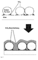
- the smaller particles arrange around the larger ones, as in FIG FIG. 1 shown schematically.
- scattering values ("haze") can be achieved, which at more than 85% and with repeated application of the layers according to the invention are even above about 98%.
- the layers formed solely from the two types of particles are relatively rough: they may have an RMS roughness, measured with a 3D Laser Scanning Microscope Keyence VK-X200K, of about 150 nm. In a preferred embodiment of the invention, which can be combined with all the aforementioned embodiments, this roughness is reduced by the presence of an additional planarization layer.
- the planarization offers the best possible (smooth or slightly wavy) basis for further processing in the production of the optically active structures, which may be advantageous, for example, when vacuum steps (sputtering of a TCO layer such as AZO or Si) should connect. Due to the leveling, the layer loses its scattering effect only to a limited extent. Also, the thermal properties of the layer system, in particular its stability to higher temperatures (for example from about 500-600 ° C), are further improved by the planarization.
- the planarization layer consists of purely inorganic, in particular oxidic material.
- it can be applied in the form of a solution or a sol or gel, from which oxide particles in a size range of 2-25 nm can be formed as indicated above for the particles of the second kind and which can be formed from the corresponding materials, the for their preparation are mentioned above.
- a sol can be used which has been produced in known manner by the sol-gel technique from a hydrolytically condensable silane or a hydrolytically condensable titanium compound or complex.
- the planarization layer higher or lower refractive materials may be used as needed; It is also possible to use a mixture of different materials which may have different refractive indices, for example a mixture of SiO 2 and TiO 2 .
- the effective refractive index of the layer system obtained can be adjusted, for example, to reduce the refractive index contrast between the planarization layer and a TCO layer of the component in the case of application of the layer system according to the invention in combination with a component such as a solar cell, LED or OLED. This reduces the reflection at the interface between the planarization layer and the TCO, which increases the light coupling in the case of a solar cell or the light extraction in the case of LEDs or OLEDs.
- the refractive index of the Planarmaschinetik be identical to that of the TCO layer or come as close as possible. This is usually at least 1.6, preferably at least 1.7, and ideally at or near 1.8.
- the person skilled in the art knows the relationship of the volume fractions of the various mixing components for adjusting the effective refractive index, which is however not linear, see the so-called effective medium theories for calculating the effective refractive index, in particular those according to Bruggeman (also referred to as "effective medium approximation"). ).
- the leveling of the particle layer is thereby greater, the more planarization layers are applied.
- the planarization produces, depending on the number of layers applied, a smooth or slightly wavy surface which can be used as a basis for further steps in the production of the optical element (sputtering of an AZO or Si layer or the like).
- Another advantage is the use of one or more planarization layers also because they improve / improve the thermal properties of the layer system. This may be advantageous if the layer according to the invention or the layer system according to the invention is to be incorporated into an optically active structure which has to be processed at higher temperatures.
- the planarization layer is formed from or using an inorganic-organic hybrid polymer.
- the planarization can be done in many cases simpler and more effective than in a purely inorganic system because of the achievability of higher single layer thicknesses.
- Typical representatives of inorganic-organic hybrid polymers include ORMOCER®e (registered trademark of the Fraunhofer Society for the Advancement of Applied Research, Kunststoff). Such hybrid polymers are inter alia in K.-H. Haas, Advanced Engineering Materials 2 (9), 571-582 (2000 ) and K.-H. Haas, S. Amberg-Schwab and Klaus Rose, Thin Solid Films 351, 198-203 (1999 ).
- the materials are based on organically modified, hydrolytically condensable silanes, in particular alkoxysilanes, and / or organometallic compounds.
- the organically modified, hydrolytically condensable silanes can be represented by the formula R 1 a R 2 b SiX 4 - a - b describe, in which the radical R 1 a is via carbon to the silicon-bonded, unsubstituted or substituted hydrocarbon radical of an organic polymerization or addition reaction, the radical R 2 is an unsubstituted or substituted hydrocarbon radical bonded to the silicon via carbon which is not accessible to an organic polymerization or addition reaction, X is a group which undergoes a condensation reaction under hydrolytic conditions to form Si.
- O-Si bridges or OH is, a is 0, 1, 2 or 3, b is 0, 1, 2 or 3 and x is 1, 2, 3 or 4.
- the radical R 1 is referred to as an (organic) network former since it can contribute to the construction of an additional organic network;
- R 1 may comprise or consist of an acrylate, methacrylate, vinyl or allyl group.
- the carbon skeleton of this group may be continuous or interrupted by heteroatoms or groups such as O, S, NH, NHCO, CONHCO, COO or NHCOO.
- R 2 is often an optionally substituted alkyl or aryl group, but may also have a different chemical structure, provided that the attachment to the silicon via a carbon atom takes place; this group, by its presence or the number b in which it is bonded to the silicon atom, influences mechanical and other properties of the resulting network; it is therefore referred to as a network converter.
- Group X is referred to as an inorganic network former; depending on their number, smaller or larger polysiloxane oligomers, chains or three-dimensional networks are formed.
- polymer materials which are based on an inorganic network which, depending on the presence of silicon and / or other metals of the organometallic compounds Si-O-Si, Si-OM and / or MOM Links. If it contains silicon atoms, this can be described as organically modified silicic acid polycondensate or siloxane, in the case of the presence of further metallic cations as organically modified silicic acid (hetero) polycondensate.
- the mechanical properties can be influenced (by the network converters) and additional organic linkages (by the network formers) can be incorporated into the hybrid polymer.
- the ORMOCER® material can be polymerized / cross-linked organically after application and thus cured (eg via organic addition or polymerization reactions).
- the organically crosslinkable groups can be polymerized in the usual way, depending on the nature of these groups, in particular thermally or photochemically. Typical photoinitiators for this purpose are IRGACURE® 369, Lucirin TPO or Lucirin TPO-L (BASF).
- the thermal curing may, with or without the aid of thermal initiators such as AIBN (azo-bis (isobutyronitrile)) or peroxides, in the presence of such starters at their respective decomposition temperature and otherwise favorably at temperatures between 140 and 180 ° C. , respectively.
- thermal initiators such as AIBN (azo-bis (isobutyronitrile)) or peroxides, in the presence of such starters at their respective decomposition temperature and otherwise favorably at temperatures between 140 and 180 ° C. , respectively.
- thermal initiators are typically used in an amount of from 1 to 5% by weight, based on the inorganic-organic hybrid material.
- planarizing layers of an inorganic-organic hybrid polymer may additionally be added with refractive index-changing and / or scattering particles. These particles are preferably inorganic nanoparticles whose surface may optionally be modified with organic groups. The addition of such particles to the planarization layer (s) may be used in a particular way to achieve a high degree of variability in optical and mechanical properties. This results in numerous possible applications of the cured materials z. As photoresists, protective coatings, functional materials or for planarization of other surfaces.
- particles whose material has a refractive index which is higher than the refractive index of the matrix have a function of increasing the refractive index.
- a material with the higher refractive index including in particular TiO 2 and ZrO 2 .
- the particles may be isolated in the matrix but need not necessarily be. By “isolated” is to be understood that their surface is not modified with a material that is involved (possibly ionic, but especially covalent) in the matrix.
- a modification of the surface which does not allow integration into the matrix, is often favorable if agglomeration of the particles is to be prevented because they scatter the light in the agglomerated state, but no longer contribute to a change in refractive index, in particular an increase in refractive index.
- the functionalization comes via a condensation reaction, for example with a organically modified silane in question, for example, according to the rule of S.
- Scattering is provided by particles of relatively large diameters (preferably> 80 nm, more preferably> 100 nm). These may also be surface-modified, for example, to produce more stable particle dispersions in the organic solvent used for incorporation and ultimately in the matrix. In the case of the scattering particles, however, the surface modification can also be used to incorporate the particles into the matrix.
- the matrix used is an organically modified (hetero) silicic acid polycondensate having organically polymerizable groups and the particles are modified with a silane which carries the same or chemically related organically polymerizable groups, so that in the case of organic crosslinking of the matrix Particles are polymerized stable in the matrix.
- An example of an organically polymerizable group is the (meth) acrylate group, with which both the silicic acid (hetero) polycondensate or siloxane matrix and the surface of the added particles can be modified.
- the substrate for the layers and layer systems according to the invention is selected as required; it may be an inorganic or an organic substrate, which should usually be transparent to visible light.
- inorganic substrates are glasses such as borofloat, soda-lime glass, Optiwhite (with and without a barrier layer), Eagle XG, silica glass and other materials that withstand temperatures of up to 500 ° C without damage.
- the sol to be generated according to step (h) has a hydroxy-carrying and / or hydrolytically condensable or partially condensed silicon compound which carries one or more organic-polymerizable groups bonded to the silicon via carbon
- these groups can be formed by heating according to step (k). , preferably to a temperature between 120 and 200 ° C, more preferably between 140 and 180 ° C and / or before or thereafter photochemically, in particular by UV irradiation, optionally in the presence of an added photoinitiator, are organically polymerized.
- the layers and layer systems according to the invention can be used as a component of a multiplicity of optically active structures, in particular of thin-layer systems.
- they can be used as substrates on which further layers are applied, or they can serve as a conclusion of such a structure, such that the substrate on which they were applied, facing outward.
- the light scattering of the following layer systems was determined by means of the following measurement method: UV-Vis spectroscopy; Meter: Shimadzu UV-3100: Procedure: Transmission: Closed integrating sphere; scattered transmission: integrating sphere open on the back; Haze: 100 x gT / T, where gT is the scattered transmission and T is the total or total transmission.
- the roughness of the coating systems was determined using the 3D laser scanning microscope Venceen VK-X200K.
- SiO 2 particles are used according to the Werner Stöber and Arthur Fink in J. of Colloid and Interface Science 26, 62-69 (1968 ) or according to the modified route of GH Bogush et al in "Preparation of Monodisperse Silica Particles: Control of Size and Mass” in Journal of Non-Crystalline Solids 104 (1988) 95-106 made from 6364g ethanol, 750g water, 680g 25% NH 3 and 416.6g TEOS in a 10L reaction vessel. After stirring for 12 hours, about 9 liters of ethanol are removed by distillation at reduced pressure using a rotary evaporator.
- the water content of the reaction mixture is reduced to less than 0.5 wt .-%.
- the solution is diluted with ethanol to a SiO 2 solids content of about 8 wt .-% (about 1500 g Stöber sol), followed by filtration through a 15-19 micron pleated filter.
- the resulting particles have a diameter of about 520 nm.
- An SiO 2 sol was prepared by mixing 240 g of TEOS (tetraethoxysilane), 41.36 g of 0.5 M HNO 3, and 120 g of ethanol, followed by stirring for 24 hours. The resulting sol was diluted with 400 g of ethanol.
- TEOS tetraethoxysilane
- p-Vinylphenyltrimethoxysilane and dimethoxydiphenylsilane were initially introduced in a molar ratio of 1: 2 and reacted with the addition of 0.5 N hydrochloric acid in a molar ratio of water to alkoxysilanes of 1.1: 1.
- Over a reaction period of 24 h at 80 ° C then carried out hydrolysis and condensation reactions.
- the reaction mixture was taken up in ethyl acetate and then washed with 200 ml of water until neutralization. After filtration through a hydrophobic filter, the final product was obtained by distillative removal of volatiles.
- the coating system did not dissolve in the crockmeter test according to EN ISO 105-X12 and is thus to be rated as “stable".
- the scattering effect of the layer system was unsatisfactory: In a 5-layer structure according to Preparation Example B1., Once as under B2. coated, the haze dropped to 11%. When only one layer of Stöber particles was used, it dropped to 2%. In general, it can be deduced from this that the less "Stöber" layers and / or the more layers of Production Example 2 are used, the more the haze sinks.
- the sol prepared was sonicated for about 10 minutes (ultrasonic bath: Bandelin Sonorex Super RK1028H, HF frequency 35kHz, RF power 300 / 600W, the sonication time was 10 minutes) and then used to measure borosilicate glasses 10 cm x 10 cm x 3.3 mm, previously rinse-cleaned using Neodisher A8 at 93 ° C at a pull rate of 30 cm / min. to submit to a dip coating.
- the glasses were then dried in the air for about 1 min.
- the glasses were then baked in the muffle furnace heated to 550 ° C for 10 minutes and then removed from the oven and allowed to cool to ambient temperature.
- FIG. 1 The structure of the resulting layer is in FIG. 1 shown schematically.
- high refractive index TiO 2 As the material for the smaller diameter particles, the light scattering increased compared to the B2 film system. strong.
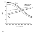
- FIG. 3 shows a diagram indicating the light scattering of different layers at different wavelengths.
- Layer system B3. is assigned to the curve "0" (without additional SiO 2 coatings). It can be seen from this that the value of haze at a wavelength of 550 nm is 87%. The roughness of this layer was 156 nm.
- Example B3-1 Glasses coated according to Example B3-1 were coated by dip coating with a sol prepared according to A2. was made. The pulling rate was 6 cm / min. After application, the coated glass was air-dried for about 1 minute, placed in a muffle furnace heated to 550 ° C for 10 minutes, and then allowed to cool to ambient temperature.
- the layer thickness of the planarization layer was about 100 nm FIG. 2 As can be seen, the ability of the layer system to scatter light decreased only slightly, namely by about 4%, by the application of the planarization layer at 550 nm.
- Example B3-1 Glasses coated according to Example B3-1 were spin coated with a lacquer prepared according to A4-2.
- the layer thickness of the paint before drying was 2-3 ⁇ m. After drying, a roughness of 1 nm was measured.
- the paint prepared according to Preparation Example A5 was used for the planarization of glasses, which were prepared according to Example B3-1. had been coated. After application, the paint was cured either thermally or light-induced. The thermal curing was carried out without additional starter at temperatures of 140-180 ° C.
- the lacquer was first mixed with Lucirin TPO (2,4,6-trimethylbenzoyl diphenylphosphine oxide) (manufactured by BASF). After coating, the coated layers were then light-induced cured and thermally post-cured with heat at 120-150 ° C. After curing, a roughness of ⁇ 10 nm was measured in each case.
Landscapes
- Physics & Mathematics (AREA)
- General Physics & Mathematics (AREA)
- Optics & Photonics (AREA)
- Chemical & Material Sciences (AREA)
- Dispersion Chemistry (AREA)
- Electroluminescent Light Sources (AREA)
- Laminated Bodies (AREA)
- Paints Or Removers (AREA)
Applications Claiming Priority (1)
| Application Number | Priority Date | Filing Date | Title |
|---|---|---|---|
| DE102014107099.2A DE102014107099B4 (de) | 2014-05-20 | 2014-05-20 | Lichtstreuendes Schichtsystem, Verfahren zu seiner Herstellung und Verwendung des Schichtsystems |
Publications (2)
| Publication Number | Publication Date |
|---|---|
| EP2955553A2 true EP2955553A2 (fr) | 2015-12-16 |
| EP2955553A3 EP2955553A3 (fr) | 2016-03-16 |
Family
ID=53199818
Family Applications (1)
| Application Number | Title | Priority Date | Filing Date |
|---|---|---|---|
| EP15168499.0A Withdrawn EP2955553A3 (fr) | 2014-05-20 | 2015-05-20 | Système multicouches à diffusion lumineuse, son procédé de production et utilisation du système multicouches |
Country Status (2)
| Country | Link |
|---|---|
| EP (1) | EP2955553A3 (fr) |
| DE (1) | DE102014107099B4 (fr) |
Families Citing this family (1)
| Publication number | Priority date | Publication date | Assignee | Title |
|---|---|---|---|---|
| US20230197749A1 (en) * | 2021-12-22 | 2023-06-22 | Visera Technologies Company Ltd. | Light diffuser, image sensor package having the same, and manufacturing method thereof |
Citations (17)
| Publication number | Priority date | Publication date | Assignee | Title |
|---|---|---|---|---|
| WO2000020337A1 (fr) | 1998-10-01 | 2000-04-13 | Fraunhofer-Gesellschaft zur Förderung der angewandten Forschung e.V. | Procede pour deposer des couches d'oxyde de titane au moyen de poudres solubles |
| WO2003027015A1 (fr) | 2001-09-21 | 2003-04-03 | Merck Patent Gmbh | Nouveau sol hybride pour la realisation de couches antireflets sio2 resistantes a l'usure |
| EP1544257B1 (fr) | 2003-12-19 | 2007-08-22 | Nissan Chemical Industries, Ltd. | Procédé de préparation de Sol d oxyde inorganique |
| US20080020860A1 (en) | 2004-03-01 | 2008-01-24 | Bridgestone Sports Co., Ltd. | Golf club head |
| US20080043403A1 (en) | 2006-01-12 | 2008-02-21 | Akira Ueda | Capacitor and manufacturing method of the same |
| WO2009011961A2 (fr) | 2007-07-13 | 2009-01-22 | 3M Innovative Properties Company | Film d'extraction de lumière pour dispositifs d'affichage à diodes électroluminescentes organiques |
| US20100150513A1 (en) | 2008-12-17 | 2010-06-17 | 3M Innovative Properties Company | Light extraction film with nanoparticle coatings |
| WO2012017183A1 (fr) | 2010-08-06 | 2012-02-09 | Saint-Gobain Glass France | Support a couche diffusante pour dispositif a diode electroluminescente organique, dispositif electroluminescent organique comportant un tel support |
| US20120234460A1 (en) | 2011-03-17 | 2012-09-20 | 3M Innovative Properties Company | Oled light extraction films having nanoparticles and periodic structures |
| US20120256218A1 (en) | 2011-04-11 | 2012-10-11 | Kwack Jin-Ho | Organic light emitting diode display |
| US20120305966A1 (en) | 2011-05-31 | 2012-12-06 | Electronics And Telecommunications Research Institute | Organic light emitting diode and method of fabricating the same |
| US20130082244A1 (en) | 2011-09-30 | 2013-04-04 | General Electric Company | Oled devices comprising hollow objects |
| DE102011086168A1 (de) | 2011-11-11 | 2013-05-16 | Osram Opto Semiconductors Gmbh | Organisches licht emittierendes bauelement |
| EP2613374A2 (fr) | 2010-10-07 | 2013-07-10 | Lg Chem, Ltd. | Substrat pour un élément électronique organique et procédé de production de celui-ci |
| KR20130108208A (ko) | 2012-03-23 | 2013-10-02 | 주식회사 엘지화학 | 유기전자소자용 기판 |
| CN103332031A (zh) | 2013-05-30 | 2013-10-02 | 合肥京东方光电科技有限公司 | 一种印刷版、散射膜层及其制作方法、显示装置 |
| EP2645442A2 (fr) | 2012-03-27 | 2013-10-02 | Moser Baer India Ltd. | Textures de gestion de lumière multiples |
Family Cites Families (6)
| Publication number | Priority date | Publication date | Assignee | Title |
|---|---|---|---|---|
| US20060286395A1 (en) * | 2005-06-15 | 2006-12-21 | Konica Minolta Medical & Graphic, Inc. | Optical film and support thereof |
| CN101118291B (zh) * | 2006-08-04 | 2010-04-14 | 鸿富锦精密工业(深圳)有限公司 | 扩散片 |
| CN101126822B (zh) * | 2006-08-18 | 2010-09-29 | 鸿富锦精密工业(深圳)有限公司 | 光学板及采用该光学板的背光模组 |
| CN101567274B (zh) * | 2009-05-21 | 2011-09-14 | 长兴化学工业股份有限公司 | 使用复合半导体材料的染敏太阳能电池 |
| US9360747B2 (en) * | 2012-03-02 | 2016-06-07 | Mitsubishi Paper Mills Limited | Transmission type screen |
| JP6039962B2 (ja) * | 2012-08-01 | 2016-12-07 | 日本板硝子株式会社 | 光電変換装置用カバーガラス |
-
2014
- 2014-05-20 DE DE102014107099.2A patent/DE102014107099B4/de active Active
-
2015
- 2015-05-20 EP EP15168499.0A patent/EP2955553A3/fr not_active Withdrawn
Patent Citations (17)
| Publication number | Priority date | Publication date | Assignee | Title |
|---|---|---|---|---|
| WO2000020337A1 (fr) | 1998-10-01 | 2000-04-13 | Fraunhofer-Gesellschaft zur Förderung der angewandten Forschung e.V. | Procede pour deposer des couches d'oxyde de titane au moyen de poudres solubles |
| WO2003027015A1 (fr) | 2001-09-21 | 2003-04-03 | Merck Patent Gmbh | Nouveau sol hybride pour la realisation de couches antireflets sio2 resistantes a l'usure |
| EP1544257B1 (fr) | 2003-12-19 | 2007-08-22 | Nissan Chemical Industries, Ltd. | Procédé de préparation de Sol d oxyde inorganique |
| US20080020860A1 (en) | 2004-03-01 | 2008-01-24 | Bridgestone Sports Co., Ltd. | Golf club head |
| US20080043403A1 (en) | 2006-01-12 | 2008-02-21 | Akira Ueda | Capacitor and manufacturing method of the same |
| WO2009011961A2 (fr) | 2007-07-13 | 2009-01-22 | 3M Innovative Properties Company | Film d'extraction de lumière pour dispositifs d'affichage à diodes électroluminescentes organiques |
| US20100150513A1 (en) | 2008-12-17 | 2010-06-17 | 3M Innovative Properties Company | Light extraction film with nanoparticle coatings |
| WO2012017183A1 (fr) | 2010-08-06 | 2012-02-09 | Saint-Gobain Glass France | Support a couche diffusante pour dispositif a diode electroluminescente organique, dispositif electroluminescent organique comportant un tel support |
| EP2613374A2 (fr) | 2010-10-07 | 2013-07-10 | Lg Chem, Ltd. | Substrat pour un élément électronique organique et procédé de production de celui-ci |
| US20120234460A1 (en) | 2011-03-17 | 2012-09-20 | 3M Innovative Properties Company | Oled light extraction films having nanoparticles and periodic structures |
| US20120256218A1 (en) | 2011-04-11 | 2012-10-11 | Kwack Jin-Ho | Organic light emitting diode display |
| US20120305966A1 (en) | 2011-05-31 | 2012-12-06 | Electronics And Telecommunications Research Institute | Organic light emitting diode and method of fabricating the same |
| US20130082244A1 (en) | 2011-09-30 | 2013-04-04 | General Electric Company | Oled devices comprising hollow objects |
| DE102011086168A1 (de) | 2011-11-11 | 2013-05-16 | Osram Opto Semiconductors Gmbh | Organisches licht emittierendes bauelement |
| KR20130108208A (ko) | 2012-03-23 | 2013-10-02 | 주식회사 엘지화학 | 유기전자소자용 기판 |
| EP2645442A2 (fr) | 2012-03-27 | 2013-10-02 | Moser Baer India Ltd. | Textures de gestion de lumière multiples |
| CN103332031A (zh) | 2013-05-30 | 2013-10-02 | 合肥京东方光电科技有限公司 | 一种印刷版、散射膜层及其制作方法、显示装置 |
Non-Patent Citations (35)
| Title |
|---|
| "Fourfold power efficiency improvement in organic light-emitting devices using an embedded nanocomposite scattering layer", ORGANIC ELECTRONICS, vol. 13, no. 6, 2012, pages 1073 - 1080 |
| "OLEDs integrated with internal scattering structure for enhancing optical out-coupling", FROM DIGEST OF TECHNICAL PAPERS - SOCIETY FOR INFORMATION DISPLAY INTERNATIONAL SYMPOSIUM, vol. 41, 2010, pages 50 - 53 |
| "Using an embedded nanocomposite scattering film for increasing out-coupling of white phosphorescent organic light-emitting devices", PROCEEDINGS OF SPIE (2912, vol. 8476, pages 84761T,1 - 84761T,6 |
| ANDREA FELTRIN ET AL.: "Advanced light trapping designs for high efficiency thin film silicon solarcells", SOLAR ENERGY MATERIALS & SOLAR CELLS, vol. 119, 2013, pages 219 - 227, XP028726778, DOI: doi:10.1016/j.solmat.2013.07.012 |
| BAS B. VAN AKEN ET AL.: "Inline deposited thin-film silicon solar cells on imprinted foil using linear PECVD sources", JOURNAL OF NON-CRYSTALLINE SOLIDS, vol. 358, 2012, pages 2268 - 2271 |
| CHANG ET AL.: "Bidirectional organic light-emitting diodes with nanoparticle-enhanced light outcoupling", FROM LASER & PHOTONICS REVIEWS, vol. 7, no. 6, 2013, pages 1079 - 1087 |
| CHIH-MING CHANG ET AL., MACROMOL. MATER. ENG., vol. 291, 2006, pages 1521 - 1528 |
| CORSIN BATTAGLIA ET AL.: "Efficient light management scheme for thin film silicon solar cells via transparent random nanostructures fabricated by nanoimprinting", APPLIED PHYSICS LETTERS, vol. 96, 2010, pages 213504, XP012131365, DOI: doi:10.1063/1.3432739 |
| DE JONG, M. M. ET AL.: "Scattering, diffraction, and geometric light trapping in thin film amorphous silionc solar cells on plastic substrates", MRS ONLIE PROCEEDINGS LIBRARY, 2012, pages 1426 |
| FENG LIU; JEAN-MICHEL NUNZI: "Enhanced organic light emitting diode and solar cell performances using silver nanoclusters Ag", ORGANIC ELECTRONICS, vol. 13, 2012, pages 1623 - 1632, XP028505146, DOI: doi:10.1016/j.orgel.2012.04.027 |
| G. H. BOGUSH ET AL.: "Preparation of Monodisperse Silica Particles: Control of Size and Mass", JOURNAL OF NON-CRYSTALLINE SOLIDS, vol. 104, 1988, pages 95 - 106, XP024357851, DOI: doi:10.1016/0022-3093(88)90187-1 |
| HITOSHI SAI ET AL.: "Flattened Light-Scattering Substrate and Its Application to Thin-Film Silicon Solar Cells", JAPANESE JOURNAL OF APPLIED PHYSICS, vol. 51, 2012, pages 10NB07 |
| HYUN, WOO JIN ET AL., JOURNAL OF INFORMATION DISPLAY, vol. 13, no. 4, 2012, pages 151 - 157 |
| J.HÜPKES; J.OWEN; S.PUST; E.BUNTE: "Chemical etching of zink oxide for thin film silicon solar cells", CHEM.PHYS.CHEM., vol. 13, 2012, pages 66 - 73 |
| JOONDONG KIM ET AL.: "Effective light management of three-dimensionally patterned transparent conductive oxide layers", APPLIED PHYSICS LETTERS, vol. 101, 2012, pages 143904, XP012165203, DOI: doi:10.1063/1.4756940 |
| JORDI ESCARRE ET AL.: "High fidelity transfer of nanometric random textures by UV embossing for thin film solar cells applications", SOLAR ENERGY MATERIALS & SOLAR CELLS, vol. 95, 2011, pages 881 - 886, XP055106637, DOI: doi:10.1016/j.solmat.2010.11.010 |
| JULIAN HAUSS ET AL.: "Metallic Bragg-gratings for light management in organic light-emitting devices", APPLIED PHYSICS LETTERS, vol. 99, no. 10, 2011, pages 103303,1 - 103303,3, XP012152314, DOI: doi:10.1063/1.3631728 |
| K.-H. HAAS, ADVANCED ENGINEERING MATERIALS, vol. 2, no. 9, 2000, pages 571 - 582 |
| K.-H. HAAS; S. AMBERG-SCHWAB; KLAUS ROSE, THIN SOLID FILMS, vol. 351, 1999, pages 198 - 203 |
| LOEBL ET AL.: "Hybrid white OLEDs for general lighting", DIGEST OF TECHNICAL PAPERS - SOCIETY FOR INFORMATION DISPLAY INTERNATIONAL SYMPOSIUM, vol. 42, 2011, pages 979 - 982 |
| MATHIEU BOCCARD ET AL.: "Multiscale Transparent Electrode Architecture for Efficient Light Management and Carrier Collection in Solar Cells", NANO LETT., vol. 12, 2012, pages 1344 - 1348 |
| MIN-AN TSAI ET AL.: "Embedded biomimetic nanostructures for enhanced optical absorption in thin-film solar cells", OPTICS EXPRESS, vol. 19, no. S4, pages A757 - A762 |
| P. LÖBMANN, J. OF SOL-GEL SCIENCE AND TECHNOLOGY, vol. 300, 2005, pages 275 - 282 |
| P. LÖBMANN, J. OF SOL-GEL SCIENCE AND TECHNOLOGY, vol. 33, 2005, pages 275 - 282 |
| S. ZHOU ET AL., LANGMUIR, vol. 23, 2007, pages 9178 - 9187 |
| SHUMING CHEN ET AL.: "One-step fabrication of organic nanoparticles as scattering media for extracting substrate waveguide light from organic light-emitting diodes", J. MATER. CHEM., vol. 22, 2012, pages 13386 |
| SÖDERSTRÖM ET AL.: "Experimental study of flat lightscattering substrates in thin-film silicon solar cells", SOLAR ENERGY MATERIALS & SOLAR CELLS, vol. 101, 2012, pages 193 - 199 |
| SU SEONG JEONG; JAE-HYEON KO: "Optical Simulation Study on the Effect of Diffusing Substrate and Pillow Lenses on the Outcoupling Efficiency of Organic Light Emitting Diodes", JOURNAL OF THE OPTICAL SOCIETY OF KOREA, vol. 17, no. 3, 2013, pages 269 - 274, XP055271608, DOI: doi:10.3807/JOSK.2013.17.3.269 |
| VON HONG-WEI CHANG ET AL.: "Nano-particle based scattering layers for optical efficiency enhancement of organic light-emitting diodes and organic solar cells", J. APPL. PHYSICS, vol. 113, no. 20, pages 204502,1 - 204502,8 |
| WERNER STÖBER; ARTHUR FINK, J. OF COLLOID AND INTERFACE SCIENCE, vol. 26, 1968, pages 62 - 69 |
| WERNER STÖBER; ARTHUR FINK, J., COLLOIC AND INTERFACE SCIENCE, vol. 26, 1962, pages 62 - 69 |
| YAN GU ET AL.: "Light extraction enhancement in organic light-emitting diodes based on localized surface plasmon and light scattering double-effect", J. MATER. CHEM. C, vol. 1, 2013, pages 4319 |
| YANG ET AL.: "Efficient optical absorption in thin-film solar cells", OPTICS EXPRESS, vol. 19, no. S5, 12 September 2011 (2011-09-12), pages A1166 |
| YU.A. AKIMOV ET AL.: "Enhancement of optical absorption in thin-film solar cells through the excitation of higher-order nanoparticle plasmon modes", OPTICS EXPRESS, vol. 17, no. 12, pages 10195, XP055170415, DOI: doi:10.1364/OE.17.010195 |
| ZHU ET AL.: "Nanodome Solar Cells with Efficient Light Management and Self-Cleaning", NANO LETT., vol. 10, 2010, pages 1979 - 1984, XP002632310, DOI: doi:10.1021/nl9034237 |
Also Published As
| Publication number | Publication date |
|---|---|
| DE102014107099B4 (de) | 2019-10-31 |
| EP2955553A3 (fr) | 2016-03-16 |
| DE102014107099A1 (de) | 2015-11-26 |
Similar Documents
| Publication | Publication Date | Title |
|---|---|---|
| EP1525338B1 (fr) | Substrat pourvu d'une couche de tio2 photocatalytique | |
| KR101503704B1 (ko) | 높은 광추출 성능을 갖는 무기미립자 산란막 | |
| DE3042770C2 (fr) | ||
| KR101887245B1 (ko) | 무기 산화물 코팅 | |
| KR102445099B1 (ko) | 철 함유 루틸형 산화티탄 미립자 분산액의 제조방법, 철 함유 루틸형 산화티탄 미립자 및 그의 용도 | |
| JP5651477B2 (ja) | ハイブリッドビヒクル系 | |
| WO2012032868A1 (fr) | Procédé de fabrication de particules de titane à surface modifiée, dispersion de particules de titane, et résine dans laquelle des particules de titane sont dispersées | |
| US20150024182A1 (en) | Antireflective Coatings with Self-Cleaning, Moisture Resistance and Antimicrobial Properties | |
| DE69816273T2 (de) | Anorganisches polymermaterial auf der basis von tantaloxyd , insbesondere mit erhöhtem brechungsindex , mechanisch verschleissfest , sein verfahren zur herstellung | |
| KR20160111435A (ko) | 반사방지 구조체를 형성하기 위한 라미네이션 전사 필름 | |
| EP2367762A1 (fr) | Nanoparticules de dioxyde de titane avec un c ur cristallin, une écorce faite d'un oxyde métallique et une peau externe qui porte des groupes organiques, ainsi que procédé pour sa fabrication | |
| DE102010052033A1 (de) | Verfahren zur Herstellung von metallischen Strukturen | |
| EP3430085B1 (fr) | Matériaux pour encapsulation de del | |
| DE102014107099B4 (de) | Lichtstreuendes Schichtsystem, Verfahren zu seiner Herstellung und Verwendung des Schichtsystems | |
| JP7150727B2 (ja) | ドープナノ粒子の製造及びその使用 | |
| WO2010086136A2 (fr) | Cellule solaire en couches minces | |
| KR101280018B1 (ko) | 고굴절률 티타니아 미세입자 제조방법 | |
| DE10235803A1 (de) | Substrate mit photokatalytischer TIO2-Schicht | |
| JP2005352121A (ja) | 反射防止膜 | |
| EP4363386A1 (fr) | Vitre ayant un revêtement sol-gel contenant des nano-inclusions | |
| DE102008010663A1 (de) | Alkalimetall und/oder Erdalkalimetall dotierte Titanoxid-Nano-Partikel sowie Verfahren zu deren Herstellung | |
| DE102010006813A1 (de) | Dünnschichtsolarzelle | |
| CN121784873A (zh) | 一种透明钛基高折射率微纳光学元器件及其制备方法 | |
| WO1998026009A1 (fr) | Matrices renfermant du carbone, leurs procedes de production et d'utilisation | |
| DE102010044132A1 (de) | Solarzelle mit einer homogenen Lichteinfangstruktur und Verfahren zur Herstellung derselben |
Legal Events
| Date | Code | Title | Description |
|---|---|---|---|
| PUAI | Public reference made under article 153(3) epc to a published international application that has entered the european phase |
Free format text: ORIGINAL CODE: 0009012 |
|
| AK | Designated contracting states |
Kind code of ref document: A2 Designated state(s): AL AT BE BG CH CY CZ DE DK EE ES FI FR GB GR HR HU IE IS IT LI LT LU LV MC MK MT NL NO PL PT RO RS SE SI SK SM TR |
|
| AX | Request for extension of the european patent |
Extension state: BA ME |
|
| PUAL | Search report despatched |
Free format text: ORIGINAL CODE: 0009013 |
|
| AK | Designated contracting states |
Kind code of ref document: A3 Designated state(s): AL AT BE BG CH CY CZ DE DK EE ES FI FR GB GR HR HU IE IS IT LI LT LU LV MC MK MT NL NO PL PT RO RS SE SI SK SM TR |
|
| AX | Request for extension of the european patent |
Extension state: BA ME |
|
| RIC1 | Information provided on ipc code assigned before grant |
Ipc: F21V 8/00 20060101ALI20160205BHEP Ipc: G02B 5/02 20060101ALI20160205BHEP Ipc: G02B 6/00 20060101AFI20160205BHEP |
|
| STAA | Information on the status of an ep patent application or granted ep patent |
Free format text: STATUS: THE APPLICATION IS DEEMED TO BE WITHDRAWN |
|
| 18D | Application deemed to be withdrawn |
Effective date: 20160917 |