EP2955753A2 - Gestapelter bildsensor mit farbteilerelement und bildaufnahmevorrichtung mit dem gestapelten bildsensor - Google Patents
Gestapelter bildsensor mit farbteilerelement und bildaufnahmevorrichtung mit dem gestapelten bildsensor Download PDFInfo
- Publication number
- EP2955753A2 EP2955753A2 EP15171727.9A EP15171727A EP2955753A2 EP 2955753 A2 EP2955753 A2 EP 2955753A2 EP 15171727 A EP15171727 A EP 15171727A EP 2955753 A2 EP2955753 A2 EP 2955753A2
- Authority
- EP
- European Patent Office
- Prior art keywords
- pixels
- light
- sensing layer
- light sensing
- image sensor
- Prior art date
- Legal status (The legal status is an assumption and is not a legal conclusion. Google has not performed a legal analysis and makes no representation as to the accuracy of the status listed.)
- Granted
Links
Images



Classifications
-
- H—ELECTRICITY
- H10—SEMICONDUCTOR DEVICES; ELECTRIC SOLID-STATE DEVICES NOT OTHERWISE PROVIDED FOR
- H10F—INORGANIC SEMICONDUCTOR DEVICES SENSITIVE TO INFRARED RADIATION, LIGHT, ELECTROMAGNETIC RADIATION OF SHORTER WAVELENGTH OR CORPUSCULAR RADIATION
- H10F39/00—Integrated devices, or assemblies of multiple devices, comprising at least one element covered by group H10F30/00, e.g. radiation detectors comprising photodiode arrays
- H10F39/10—Integrated devices
- H10F39/12—Image sensors
- H10F39/18—Complementary metal-oxide-semiconductor [CMOS] image sensors; Photodiode array image sensors
- H10F39/182—Colour image sensors
- H10F39/1825—Multicolour image sensors having stacked structure, e.g. NPN, NPNPN or multiple quantum well [MQW] structures
-
- G—PHYSICS
- G02—OPTICS
- G02B—OPTICAL ELEMENTS, SYSTEMS OR APPARATUS
- G02B5/00—Optical elements other than lenses
- G02B5/20—Filters
- G02B5/201—Filters in the form of arrays
-
- H—ELECTRICITY
- H10—SEMICONDUCTOR DEVICES; ELECTRIC SOLID-STATE DEVICES NOT OTHERWISE PROVIDED FOR
- H10F—INORGANIC SEMICONDUCTOR DEVICES SENSITIVE TO INFRARED RADIATION, LIGHT, ELECTROMAGNETIC RADIATION OF SHORTER WAVELENGTH OR CORPUSCULAR RADIATION
- H10F39/00—Integrated devices, or assemblies of multiple devices, comprising at least one element covered by group H10F30/00, e.g. radiation detectors comprising photodiode arrays
- H10F39/011—Manufacture or treatment of image sensors covered by group H10F39/12
- H10F39/024—Manufacture or treatment of image sensors covered by group H10F39/12 of coatings or optical elements
-
- H—ELECTRICITY
- H10—SEMICONDUCTOR DEVICES; ELECTRIC SOLID-STATE DEVICES NOT OTHERWISE PROVIDED FOR
- H10F—INORGANIC SEMICONDUCTOR DEVICES SENSITIVE TO INFRARED RADIATION, LIGHT, ELECTROMAGNETIC RADIATION OF SHORTER WAVELENGTH OR CORPUSCULAR RADIATION
- H10F39/00—Integrated devices, or assemblies of multiple devices, comprising at least one element covered by group H10F30/00, e.g. radiation detectors comprising photodiode arrays
- H10F39/80—Constructional details of image sensors
- H10F39/802—Geometry or disposition of elements in pixels, e.g. address-lines or gate electrodes
-
- H—ELECTRICITY
- H10—SEMICONDUCTOR DEVICES; ELECTRIC SOLID-STATE DEVICES NOT OTHERWISE PROVIDED FOR
- H10F—INORGANIC SEMICONDUCTOR DEVICES SENSITIVE TO INFRARED RADIATION, LIGHT, ELECTROMAGNETIC RADIATION OF SHORTER WAVELENGTH OR CORPUSCULAR RADIATION
- H10F39/00—Integrated devices, or assemblies of multiple devices, comprising at least one element covered by group H10F30/00, e.g. radiation detectors comprising photodiode arrays
- H10F39/80—Constructional details of image sensors
- H10F39/805—Coatings
- H10F39/8053—Colour filters
-
- H—ELECTRICITY
- H10—SEMICONDUCTOR DEVICES; ELECTRIC SOLID-STATE DEVICES NOT OTHERWISE PROVIDED FOR
- H10F—INORGANIC SEMICONDUCTOR DEVICES SENSITIVE TO INFRARED RADIATION, LIGHT, ELECTROMAGNETIC RADIATION OF SHORTER WAVELENGTH OR CORPUSCULAR RADIATION
- H10F39/00—Integrated devices, or assemblies of multiple devices, comprising at least one element covered by group H10F30/00, e.g. radiation detectors comprising photodiode arrays
- H10F39/80—Constructional details of image sensors
- H10F39/806—Optical elements or arrangements associated with the image sensors
-
- H—ELECTRICITY
- H10—SEMICONDUCTOR DEVICES; ELECTRIC SOLID-STATE DEVICES NOT OTHERWISE PROVIDED FOR
- H10F—INORGANIC SEMICONDUCTOR DEVICES SENSITIVE TO INFRARED RADIATION, LIGHT, ELECTROMAGNETIC RADIATION OF SHORTER WAVELENGTH OR CORPUSCULAR RADIATION
- H10F39/00—Integrated devices, or assemblies of multiple devices, comprising at least one element covered by group H10F30/00, e.g. radiation detectors comprising photodiode arrays
- H10F39/80—Constructional details of image sensors
- H10F39/811—Interconnections
-
- H—ELECTRICITY
- H10—SEMICONDUCTOR DEVICES; ELECTRIC SOLID-STATE DEVICES NOT OTHERWISE PROVIDED FOR
- H10F—INORGANIC SEMICONDUCTOR DEVICES SENSITIVE TO INFRARED RADIATION, LIGHT, ELECTROMAGNETIC RADIATION OF SHORTER WAVELENGTH OR CORPUSCULAR RADIATION
- H10F39/00—Integrated devices, or assemblies of multiple devices, comprising at least one element covered by group H10F30/00, e.g. radiation detectors comprising photodiode arrays
- H10F39/011—Manufacture or treatment of image sensors covered by group H10F39/12
- H10F39/018—Manufacture or treatment of image sensors covered by group H10F39/12 of hybrid image sensors
-
- H—ELECTRICITY
- H10—SEMICONDUCTOR DEVICES; ELECTRIC SOLID-STATE DEVICES NOT OTHERWISE PROVIDED FOR
- H10F—INORGANIC SEMICONDUCTOR DEVICES SENSITIVE TO INFRARED RADIATION, LIGHT, ELECTROMAGNETIC RADIATION OF SHORTER WAVELENGTH OR CORPUSCULAR RADIATION
- H10F39/00—Integrated devices, or assemblies of multiple devices, comprising at least one element covered by group H10F30/00, e.g. radiation detectors comprising photodiode arrays
- H10F39/80—Constructional details of image sensors
- H10F39/806—Optical elements or arrangements associated with the image sensors
- H10F39/8067—Reflectors
-
- H—ELECTRICITY
- H10—SEMICONDUCTOR DEVICES; ELECTRIC SOLID-STATE DEVICES NOT OTHERWISE PROVIDED FOR
- H10F—INORGANIC SEMICONDUCTOR DEVICES SENSITIVE TO INFRARED RADIATION, LIGHT, ELECTROMAGNETIC RADIATION OF SHORTER WAVELENGTH OR CORPUSCULAR RADIATION
- H10F39/00—Integrated devices, or assemblies of multiple devices, comprising at least one element covered by group H10F30/00, e.g. radiation detectors comprising photodiode arrays
- H10F39/80—Constructional details of image sensors
- H10F39/809—Constructional details of image sensors of hybrid image sensors
Definitions
- An apparatus and a sensor consistent with exemplary embodiments broadly relate to a stacked type image sensor including a color separation element and an image pickup apparatus including the image sensor, and more particularly, to a stacked type image sensor having improved light use efficiency due to use of a color separation element, and an image pickup apparatus including the image sensor.
- color displays display multicolor images and color image sensors detect colors of incident light thereon by using color filters.
- Most of the currently used color displays or color image sensors use a RGB color filter scheme in which, for example, green filters are disposed to correspond to two of four pixels and blue and red filters are disposed to correspond to the other two pixels.
- a CYGM color filter scheme in which complementary cyan, yellow, green, and magenta color filters are respectively disposed to correspond to four pixels is used.
- the color filters absorb all colors of light except for a filtered color, the light use efficiency of the color filters may be low. For example, since RGB color filters transmit only about 1/3 of incident light and absorb about 2/3 of the incident light, the light use efficiency of the RGB color filters is only about 33%. Therefore, most of the optical loss of the color displays or color image sensors is caused by the color filters.
- an image sensor includes: a first light sensing layer including a plurality of first pixels absorbing light of a first wavelength band and transmitting light of other wavelength bands; a second light sensing layer positioned to face the first light sensing layer, the second light sensing layer including a plurality of second pixels detecting light of a second wavelength band from the transmitted other wavelength bands and a plurality of third pixels detecting light of a third wavelength band from the transmitted other wavelength bands; and a plurality of color separation elements positioned between the first light sensing layer and the second light sensing layer, the color separation elements being configured to direct light of the second wavelength band toward the second pixels and direct light of the third wavelength band toward the third pixels.
- the first pixels of the first light sensing layer may be arranged in a two-dimensional array, and the second and third pixels of the second light sensing layer may be alternately arranged in a two-dimensional array.
- the first to third pixels may have the same size, and the first light sensing layer and the second light sensing layer may be arranged such that boundaries of the first pixels may be aligned with boundaries of the second and third pixels.
- the first light sensing layer and the second light sensing layer may be shifted relative to each other such that the first pixels may overlap portions of the second pixels and portions of the third pixels.
- the second light sensing layer may include: first pixel rows in which a plurality of the second pixels and a plurality of the third pixels are alternately arranged in a first direction; and second pixel rows in which another plurality of the third pixels and another plurality of the second pixels are alternately arranged in the first direction, wherein the first and second pixel rows may be alternately arranged in a second direction perpendicular to the first direction.
- the image sensor may further include a plurality of driving signal lines extending from the first light sensing layer to the second light sensing layer, which perform one of more of transmitting driving signals to the first light sensing layer and receiving data signals from the first light sensing layer.
- the driving signal lines may be arranged outside main propagation paths of light separated by the color separation elements.
- the driving signal lines may be arranged between the color separation elements in diagonal directions with respect to the color separation elements.
- the driving signal lines may be arranged along interfaces between the first pixel rows and the second pixel rows.
- the image sensor may further include trenches positioned between the second and third pixels, wherein the driving signal lines may extend from the first light sensing layer to the trenches positioned between the second and third pixels.
- the color separation elements may be respectively positioned above the second pixels, and may be configured to direct the light of the second wavelength band in a straight downward direction towards the second pixels and the light of the third wavelength band toward both sides of the respective color separation element and towards the third pixels.
- the color separation elements may be respectively positioned above the third pixels, and may be configured to direct the light of the third wavelength band in a straight downward direction toward the third pixels and the light of the second wavelength band toward both sides of the respective color separation elements toward the second pixels.
- the color separation elements may be positioned to respectively face interfaces between the second and third pixels, and may be configured to direct the light of the second wavelength band toward a first peripheral side of the respective color separation element toward the respective second pixel and the light of the third wavelength band toward the other peripheral side, which is opposite the first peripheral side of the respective color separation element toward the respective third pixel.
- the image sensor may further include a color filter layer, wherein the color filter layer may include: second color filters positioned on top of the second pixels and only transmitting the light of the second wavelength band; and third color filters positioned on top of the third pixels and only transmitting the light of the third wavelength band.
- the color filter layer may include: second color filters positioned on top of the second pixels and only transmitting the light of the second wavelength band; and third color filters positioned on top of the third pixels and only transmitting the light of the third wavelength band.
- the image sensor may further include a transparent dielectric layer positioned between the first light sensing layer and the second light sensing layer, wherein the color separation elements may be buried in and fixed into the transparent dielectric layer.
- the color separation elements may be formed of a material having a refractive index greater than that of the transparent dielectric layer.
- an image pickup apparatus includes the image sensor such as the one described above.
- a stacked type image sensor including a color separation element and an image pickup apparatus including the image sensor will be described in detail with reference to the accompanying drawings.
- like reference numbers refer to like elements, and also the size of each element may be exaggerated for clarity of illustration. Exemplary embodiments described herein are for illustrative purposes only, and various modifications may be made therefrom.
- when an element is referred to as being "above” or "on” another element in a layered structure it may be directly on the other element while making contact with the other element or may be above the other element without making contact with the other element.
- FIG. 1 is a view schematically illustrating a structure of an image sensor 100 according to an exemplary embodiment.
- the image sensor 100 of an exemplary embodiment may include a first light sensing layer 140 including a plurality of first pixels Px1 absorbing and detecting light of a first wavelength band and transmitting light of other wavelength bands, a second light sensing layer 110 including a plurality of second pixels Px2 detecting light of a second wavelength band and a plurality of third pixels Px3 detecting light of a third wavelength band, and color separation elements 130 may be positioned between the first light sensing layer 140 and the second light sensing layer 110.
- the color separation elements 130 may direct a second wavelength band of light passed through the first light sensing layer 140 toward the second pixels Px2 of the second light sensing layer 110, and a third wavelength band of the light passed through the first light sensing layer 140 toward the third pixels Px3 of the second light sensing layer 110, in an exemplary embodiment.
- the image sensor 100 may further include a transparent dielectric layer 120 positioned between the first light sensing layer 140 and the second light sensing layer 110, a first transparent electrode 141 and a second transparent electrode 142, respectively positioned on a lower surface and an upper surface of the first light sensing layer 140, and a plurality of microlenses 150 positioned on top of or above the second transparent electrode 142.
- the color separation elements 130 may be buried and fixed in the transparent dielectric layer 120.
- the first transparent electrode 141 and the second transparent electrode 142 apply a driving voltage to the first light sensing layer 140 and may be formed of, for example, a transparent conductive oxide such as indium tin oxide (ITO), indium zinc oxide (IZO), aluminum zinc oxide (AZO), or gallium zinc oxide (GZO), in an exemplary embodiment.
- a transparent conductive oxide such as indium tin oxide (ITO), indium zinc oxide (IZO), aluminum zinc oxide (AZO), or gallium zinc oxide (GZO)
- the first light sensing layer 140 and the second light sensing layer 110 may be stacked as shown in FIG. 1 in an exemplary embodiment.
- the transparent dielectric layer 120 may be positioned directly or indirectly above or on an upper surface of the second light sensing layer 110, and the first light sensing layer 140 may be positioned directly or indirectly above or on an upper surface of the transparent dielectric layer 120, parallel to the second light sensing layer 110 such that the transparent dielectric layer 120 is sandwiched between the first light sensing layer 140 and the second light sensing layer 110.
- the first light sensing layer 140 and the second light sensing layer 110 may be configured to detect different wavelength bands of light.
- the first light sensing layer 140 may absorb only light of a first wavelength band to be detected and may transmit light of second and third wavelength bands.
- the first light sensing layer 140 may absorb only light of a green wavelength band and may transmit light of red and blue wavelength bands according to an exemplary embodiment.
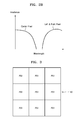
- FIG. 2A is a graph illustrating an exemplary transmission spectrum of a first light sensing layer such as the first light sensing layer 140 of the image sensor 100 illustrated in FIG. 1 .
- the first light sensing layer 140 may transmit most blue light in a 400-nm wavelength band and most red light in a 700-nm wavelength band, but may absorb most green light in a 530-nm wavelength band.
- the first light sensing layer 140 having the above-described exemplary characteristics may include a material such as rhodamine-based pigment, a merocyanine-based pigment, or quinacridone.
- the absorption wavelength band of the first light sensing layer 140 is not limited to a green wavelength band.
- the first light sensing layer 140 may only absorb and detect light of a red wavelength band and may transmit light of blue and green wavelength bands.
- the first light sensing layer 140 may only absorb light of a blue wavelength band and may transmit light of green and red wavelength bands.
- the first light sensing layer 140 may include a phthalocyanine-based pigment to detect light of a green wavelength band, or may include a material such as a coumarin-based pigment, tris-(8-hydroxyquinoline)aluminum (Alq3), or a merocyanine-based pigment to detect light of a blue wavelength band.
- Alq3 tris-(8-hydroxyquinoline)aluminum
- merocyanine-based pigment to detect light of a blue wavelength band.
- the color separation elements 130 are positioned at a light entrance side of the second light sensing layer 110 to separate incident light according to the wavelength thereof so that different wavelengths of the incident light may enter different pixels.
- the color separation elements 130 may separate colors of incident light thereon by changing the propagation direction of the incident light according to the wavelength of the incident light based on the diffraction or refraction characteristics of light varying according to the wavelength of the light.
- the color separation elements 130 may be formed of a material having a refractive index greater than that of the transparent dielectric layer 120 surrounding the color separation elements 130 according to an exemplary embodiment.
- the transparent dielectric layer 120 may be formed of SiO 2 or siloxane-based spin-on-glass (SOG), and the color separation elements 130 may be formed of a material having a high refractive index such as TiO 2 , SiN 3 , ZnS, ZnSe, or Si 3 N 4 .
- color separation elements 130 may be variously designed according to desired spectrum distributions of exiting light and are within the scope of exemplary embodiments.
- the color separation elements 130 may divide incident light thereon into light C2 of a second wavelength band and light C3 of a third wavelength band, according to an exemplary embodiment.
- the color separation elements 130 may not change the propagation direction of the light C2 of the second wavelength band and may change the propagation direction of the light C3 of the third wavelength band toward lateral sides thereof.
- the light C2 of the second wavelength band may be incident on the second pixels Px2 located under the color separation elements 130
- the light C3 of the third wavelength band may be incident on the third pixels Px3 located at lateral sides of the color separation elements 130, according to an exemplary embodiment. Therefore, the second pixels Px2 located under the color separation elements 130 may detect the light C2 of the second wavelength band, and the third pixels Px3 located at lateral sides of the color separation elements 130 may detect the light C3 of the third wavelength band, in an exemplary embodiment.
- the light C2 of the second wavelength band may be blue light
- the light C3 of the third wavelength band may be red light
- FIG. 2B is a graph illustrating an exemplary color-separation spectrum of a color separation elements such as the color separation elements 130 of the image sensor 100 illustrated in FIG. 1 , according to an exemplary embodiment.
- the color separation elements 130 may separate light of a blue wavelength band and light of a red wavelength band by directing light of the blue wavelength band in a straight downward direction and directing light of the red wavelength band toward left and right sides thereof.
- the first light sensing layer 140 may absorb and detect green light
- the second light sensing layer 110 may detect blue and red light transmitted through the first light sensing layer 140.
- the first pixels Px1 of the first light sensing layer 140 and the second and third pixels Px2 and Px3, respectively, may have the same size.
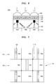
- FIG. 3 is a view schematically illustrating a pixel structure of a first light sensing layer such as the light sensing layer 140 of the image sensor 100, according to an exemplary embodiment
- FIG. 4 is a view schematically illustrating a pixel structure of a second light sensing layer such as the second light sensing layer 110 of the image sensor 100 according to an exemplary embodiment. Referring to FIGS.
- the first pixels Px1 of the first light sensing layer 140 may be arranged in a two-dimensional array structure, and the second pixels Px2 and the third pixels Px3 of the second light sensing layer 110 may be arranged in a two-dimensional array structure.
- the first pixels Px1 of the first light sensing layer 140 may match the second and third pixels Px2 and Px3 of the second light sensing layer 110 in such a manner that boundaries of the first pixels Px1 are aligned with boundaries of the second and third pixels Px2 and Px3, according to an exemplary embodiment.
- the second and third pixels Px2 and Px3 of the second light sensing layer 110 may be alternately arranged in rows and columns.
- the second light sensing layer 110 may include first pixel rows P1 in which a plurality of second pixels Px2 and a plurality of third pixels Px3 are alternately arranged in the order of second and third pixels Px2 and Px3, and second pixel rows P2 in which a plurality of third pixels Px3 and a plurality of second pixels Px2 are alternately arranged in the order of third and second pixels Px3 and Px2.
- the first pixel rows P1 and the second pixel rows P2 may be alternately arranged in a vertical direction, according to an exemplary embodiment.
- the color separation elements 130 may be positioned to face the second pixels Px2. Therefore, the color separation elements 130 may provide light C2 of a second wavelength band for the second pixels Px2, and light C3 of a third wavelength band for the third pixels Px3 which may be positioned at left and right sides thereof.
- the image sensor 100 may further include driving signal lines 115 to transmit driving signals to the first light sensing layer 140 or receive data signals from the first light sensing layer 140, according to an exemplary embodiment.
- a driving circuit (not shown in the cross-sectional view of FIG. 1 ) may be positioned below or under the second light sensing layer 110 so as to control operations of the first light sensing layer 140 and the second light sensing layer 110 and process data received from the first light sensing layer 140 and the second light sensing layer 110. Therefore, the driving signal lines 115 may penetrate the second light sensing layer 110 and the transparent dielectric layer 120 to connect the driving circuit positioned below or under the second light sensing layer 110 to the first light sensing layer 140.
- FIG. 5 is a schematic cross-sectional view of a second light sensing layer such as the second light sensing layer 100 taken along line A-A' of FIG. 4 , according to an exemplary embodiment.
- the driving signal lines 115 may extend between the second and third pixels Px2 and Px3 of the second light sensing layer 110 to the first light sensing layer 140 through the transparent dielectric layer 120. Trenches may be formed among the second and third pixels Px2 and Px3 to separate the second and third pixels Px2 and Px3, and the driving signal lines 115 may be positioned in the trenches between the second and third pixels Px2 and Px3. Also, the driving signal lines 115 may be surrounded by insulation films 116 to separate the trenches from the second and third pixels Px2 and Px3.
- the driving signal lines 115 may be placed at positions so as not to obstruct the propagation of light separated by the color separation elements 130. That is, the driving signal lines 115 may be positioned outside main propagation paths of light separated by the color separation elements 130. For example, as shown in FIG. 4 , the driving signal lines 115 may be positioned at vertexes of the second and third pixels Px2 and Px3.
- the driving signal lines 115 may be positioned among the color separation elements 130 in diagonal directions of the color separation elements 130.
- the positions of the driving signal lines 115 are not limited thereto and are provided by way of an example only. That is, the driving signal lines 115 may be placed at any positions as long as the propagation of light separated by the color separation elements 130 is not obstructed. For example, if the light separated by the color separation elements 130 propagates toward the left and right sides of the color separation elements 130, the driving signal lines 115 may be placed at any positions along interfaces between the first and second pixel rows P1 and P2 extending in a horizontal direction.
- the first light sensing layer 140 and the second light sensing layer 110 of the image sensor 100 are arranged in a stacked manner, the number of pixels per area may be increased. Therefore, the resolution of the image sensor 100 may be improved. Furthermore, the first light sensing layer 140 absorbs and detects most of the light of a first wavelength band. Also, the light of second and third wavelength bands separated by the color separation elements 130 are detected by the second light sensing layer 110 almost without a loss. Therefore, according to an exemplary embodiment, the light of the first to third wavelength bands may be efficiently used. Therefore, according to an exemplary embodiment, the sensitivity of the image sensor 100 may be improved in all wavelength bands.
- the color separation elements 130 may be configured to separate only two wavelength bands of light, and thus, the color separation elements 130 may be easily designed and manufactured.
- the image sensor 100 of an exemplary embodiment may be applied to various image pickup apparatuses for providing high-quality images.
- the image pickup apparatuses may further include a display and a memory.
- the image pickup apparatuses may be a digital still camera or a digital video camera which has a sensor for picking up an image and hardware or a combination of hardware and software processor/controller which controls the storing/recording of the image into a memory and/or outputting the image onto a display.
- the image pickup apparatuses may further include a tangible user interface for user inputting commands.
- the user interface may include a number of user buttons, which are manipulated by the user to capture, process, edit, and output images.
- the structures of the first light sensing layer 140 and the second light sensing layer 110 of the image sensor 100 and the characteristics of the color separation elements 130 described with reference to FIGS. 1 to 5 are exemplary structures and characteristics, according to an exemplary embodiment. That is, image sensors having various structures other than those described with reference to FIGS. 1 to 5 may be provided in exemplary embodiments. For example, various color-separation characteristics may be obtained according to the design of the color separation elements 130, and the structure of the second light sensing layer 110 may be changed in various ways according to the design of the color separation elements 130. Furthermore, the relative arrangement of the first light sensing layer 140 and the second light sensing layer 110 may be altered in various ways.
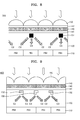
- FIG. 6 is a cross-sectional view schematically illustrating the structure of an image sensor according to yet another exemplary embodiment
- FIG. 7 is a plan view schematically illustrating a pixel structure of a second light sensing layer such as the second light sensing layer 110 of the image sensor 200, according to an exemplary embodiment.
- first and second light sensing layers 140 and 110 of the image sensor 200 illustrated in FIG. 6 are shifted relative to each other.
- the first light sensing layer 140 may be shifted relative to the second light sensing layer 110 by 1/2 of a pixel width.
- first pixels Px1 of the first light sensing layer 140 may range over halves of second and third pixels Px2 and Px3 of the second light sensing layer 110.
- the second light sensing layer 110 may have analogous pixel structure to the one illustrated in FIG. 4 , according to an exemplary embodiment.
- the first pixels Px1 of the first light sensing layer 140 may overlap portions of the second pixels Px2 and portions of the third pixels Px3.
- the resolution of the image sensor 200 may be improved by analyzing color information of the overlapping portions according to an exemplary embodiment.
- FIG. 8 is a plan view schematically illustrating a structure of an image sensor according to yet another exemplary embodiment.
- the color separation elements 130 are positioned to face the second pixels Px2 and are configured to direct light C2 of a second wavelength band in a straight downward direction and light C3 of a third wavelength band toward left and right sides thereof.
- the image sensor 300 illustrated in FIG. 8 may include color separation elements 131 configured to direct light C3 of a third wavelength band in a straight downward direction and light C2 of a second wavelength band toward left and right sides.
- the color separation elements 131 may be posited directly above third pixels Px3.
- the color separation elements 131 may direct light of a red wavelength band in a straight downward direction (that is, toward the third pixels Px3) and light of a blue wavelength band toward left and right sides (that is, toward second pixels Px2).
- Other structures of the image sensor 300 may be the analogous to those of the image sensor 100 illustrated FIG. 1 , according to an exemplary embodiment.
- the color separation elements 131 illustrated in FIG. 8 may be applied to the image sensor 200 illustrated in FIGS. 6 and 7 , according to yet another exemplary embodiment.
- FIG. 9 is a plan view schematically illustrating a structure of an image sensor according to yet another exemplary embodiment.
- the image sensor 400 illustrated in FIG. 9 may include first color separation elements 132 configured to direct light C2 of a second wavelength band toward left sides and light C3 of a third wavelength band toward right sides and second color separation elements 133 configured to direct light C3 of the third wavelength band toward left sides and light C2 of the second wavelength band toward right sides.
- the first and second color separation elements 132 and 133 may be alternately arranged to as an interface between second and third pixels Px2 and Px3 such that each of the second pixels Px2 is disposed at a left side of each of the first color separation elements 132 and at a right side of each of the second color separation elements 133 and each of the third pixels Px3 is disposed at a left side of each of the second color separation elements 133 and at a right side of each of the first color separation elements 132, as shown in FIG. 9 .
- light C2 of a second wavelength band separated by the first and second color separation elements 132 and 133 may be incident on the second pixels Px2, and light C3 of a third wavelength band separated by the first and second color separation elements 132 and 133 may be incident on the third pixels Px3.
- the first and second separation elements 132 and 133 may have an asymmetric stepwise shape such that light C2 and light C3 are asymmetrically separated by the first and second separation elements 132 and 133.
- the first and second separation elements 132 and 133 may have an identical structure but may be disposed in opposite directions to each other.
- Each of the plurality of microlenses 150 may be disposed between two adjacent first pixels Px1 such that light converged by the microlenses 150 is incident on the first and second color separation elements 132 and 133.
- Other structures of the image sensor 400 illustrated FIG. 9 may be analogous to the ones of the image sensor 100 illustrated FIG. 1 , according to an exemplary embodiment.
- the color separation elements 132 illustrated in FIG. 9 may be applied to the image sensor 200 illustrated in FIGS. 6 and 7 , according to yet another exemplary embodiment.
- color separation elements having various characteristics may be used, and the arrangement of the first light sensing layer 140 and the second light sensing layer 110 may vary according to the color-separation characteristics of the color separation elements.
- the distance between the color separation elements 130, 131, or 132 and the second light sensing layer 110 may be several micrometers or shorter, for example, 1 micrometer or shorter, according to various exemplary embodiments. Since the distance between the color separation elements 130, 131, or 132 and the second light sensing layer 110 is short, colors may not be fully separated in some cases. Thus, color filters may additionally be used to reduce the possibility of color mixing and improve color reproducibility, according to an exemplary embodiment.
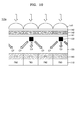
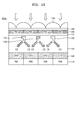
- FIGS. 10 to 12 are cross-sectional view schematically illustrating image sensors 100a, 300a, and 400a including additional color filters according to yet other exemplary embodiments.
- the image sensor 100a illustrated in FIG. 10 further includes a color filter layer 160, some of other components are analogous to the components of the image sensor 100 illustrated in FIG. 1 , according to an exemplary embodiment.
- the image sensor 300a illustrated in FIG. 11 further includes a color filter layer 160, some of other components are analogous to the components of the image sensor 300 illustrated in FIG. 8 , according to an exemplary embodiment.
- the image sensor 400a illustrated in FIG. 12 further includes a color filter layer 160, some of other components are analogous to the components of the image sensor 400 illustrated in FIG. 9 , according to an exemplary embodiment.
- the color filter layer 160 may be positioned on top of a second light sensing layer 110.
- the color filter layer 160 may include second color filters CF2 positioned on top of second pixels Px2 and transmitting only light C2 of a second wavelength band, and third color filters CF3 positioned on top of third pixels Px3 and transmitting only light C3 of a third wavelength band.
- the color filter layer 160 is used, since light C2 and light C3 significantly separated by the color separation elements 130, 131, or 132 are incident on the color filters CF2 and CF3, optical loss caused by the color filter layer 160 may not be large. Therefore, the image sensors 100a, 300a, and 400a illustrated in FIGS. 10 to 12 may have high light use efficiency and color reproducibility, according to an exemplary embodiment.
Landscapes
- Physics & Mathematics (AREA)
- General Physics & Mathematics (AREA)
- Optics & Photonics (AREA)
- Solid State Image Pick-Up Elements (AREA)
- Color Television Image Signal Generators (AREA)
Applications Claiming Priority (1)
| Application Number | Priority Date | Filing Date | Title |
|---|---|---|---|
| KR1020140072293A KR102261855B1 (ko) | 2014-06-13 | 2014-06-13 | 색분리 소자를 포함하는 적층형 이미지 센서 및 상기 이미지 센서를 포함하는 촬상 장치 |
Publications (3)
| Publication Number | Publication Date |
|---|---|
| EP2955753A2 true EP2955753A2 (de) | 2015-12-16 |
| EP2955753A3 EP2955753A3 (de) | 2016-03-30 |
| EP2955753B1 EP2955753B1 (de) | 2020-04-08 |
Family
ID=53489794
Family Applications (1)
| Application Number | Title | Priority Date | Filing Date |
|---|---|---|---|
| EP15171727.9A Active EP2955753B1 (de) | 2014-06-13 | 2015-06-11 | Gestapelter bildsensor mit farbteilerelement und bildaufnahmevorrichtung mit dem gestapelten bildsensor |
Country Status (3)
| Country | Link |
|---|---|
| US (1) | US9525006B2 (de) |
| EP (1) | EP2955753B1 (de) |
| KR (1) | KR102261855B1 (de) |
Cited By (7)
| Publication number | Priority date | Publication date | Assignee | Title |
|---|---|---|---|---|
| US11573356B2 (en) | 2018-03-13 | 2023-02-07 | Interdigital Ce Patent Holdings | Diffraction grating comprising double-materials structures |
| US11604363B2 (en) | 2018-03-13 | 2023-03-14 | Interdigital Ce Patent Holdings | Image sensor comprising a color splitter with two different refractive indexes |
| US11972508B2 (en) | 2018-07-02 | 2024-04-30 | Interdigital Ce Patent Holdings, Sas | Image sensor comprising a color splitter with two different refractive indexes, and different height |
| US12174512B2 (en) | 2018-12-18 | 2024-12-24 | Interdigital Ce Patent Holdings | Device for forming an outgoing electromagnetic wave from an incident electromagnetic wave |
| US12210155B2 (en) | 2018-06-29 | 2025-01-28 | Interdigital Ce Patent Holdings | Optical device comprising a multi-layers waveguides |
| US12214493B2 (en) | 2018-12-18 | 2025-02-04 | Interdigital Ce Patent Holdings, Sas | Optical manipulation apparatus |
| US12228756B2 (en) | 2018-12-21 | 2025-02-18 | Interdigital Ce Patent Holdings, Sas | Optical device |
Families Citing this family (14)
| Publication number | Priority date | Publication date | Assignee | Title |
|---|---|---|---|---|
| KR102338897B1 (ko) * | 2014-10-22 | 2021-12-13 | 삼성전자주식회사 | 색분리 소자를 포함하는 적층형 이미지 센서 및 상기 이미지 센서를 포함하는 촬상 장치 |
| KR102531712B1 (ko) | 2015-08-19 | 2023-05-11 | 삼성전자주식회사 | 적층형 이미지 센서와 그 제조방법 |
| KR102501643B1 (ko) * | 2015-09-24 | 2023-02-20 | 삼성전자주식회사 | 고굴절률 광학 기능층을 포함하는 광학 장치 및 상기 광학 장치의 제조 방법 |
| KR102465995B1 (ko) * | 2015-09-30 | 2022-11-25 | 삼성전자주식회사 | 색분할기 구조와 그 제조방법, 색분할기 구조를 포함하는 이미지센서 및 이미지센서를 포함하는 광학장치 |
| KR102466671B1 (ko) | 2015-10-02 | 2022-11-14 | 삼성전자주식회사 | 적층형 이미지 센서 |
| KR20170070685A (ko) * | 2015-12-14 | 2017-06-22 | 삼성전자주식회사 | 하이브리드 컬러필터를 포함한 이미지 센서 |
| KR102568789B1 (ko) | 2016-03-10 | 2023-08-21 | 삼성전자주식회사 | 무기 컬러 필터를 포함하는 컬러 필터 어레이, 상기 컬러 필터 어레이를 포함하는 이미지 센서 및 디스플레이 장치 |
| WO2017169719A1 (ja) * | 2016-03-28 | 2017-10-05 | ソニー株式会社 | 固体撮像素子、および電子機器 |
| KR102395992B1 (ko) * | 2017-04-07 | 2022-05-10 | 삼성전자주식회사 | 광대역 컬러 필터를 포함하는 이미지 센서 |
| JP7265195B2 (ja) * | 2018-04-17 | 2023-04-26 | 日本電信電話株式会社 | カラー撮像素子および撮像装置 |
| KR102634950B1 (ko) | 2019-01-11 | 2024-02-07 | 삼성전자주식회사 | 이미지 센서 |
| KR20240037960A (ko) * | 2021-08-06 | 2024-03-22 | 소니 세미컨덕터 솔루션즈 가부시키가이샤 | 촬상 장치 |
| JP2023099014A (ja) * | 2021-11-18 | 2023-07-11 | 日本電信電話株式会社 | カラー撮像素子および撮像装置 |
| JP2023152523A (ja) * | 2022-04-04 | 2023-10-17 | ソニーセミコンダクタソリューションズ株式会社 | 光検出装置 |
Family Cites Families (19)
| Publication number | Priority date | Publication date | Assignee | Title |
|---|---|---|---|---|
| US5764389A (en) * | 1996-11-26 | 1998-06-09 | Hughes Electronics Corporation | Holographic color filters for display applications, and operating method |
| JP3713418B2 (ja) * | 2000-05-30 | 2005-11-09 | 光正 小柳 | 3次元画像処理装置の製造方法 |
| US6738171B1 (en) * | 2001-11-21 | 2004-05-18 | Micron Technology, Inc. | Color filter array and microlens array having holographic optical elements |
| US8101903B2 (en) * | 2007-01-23 | 2012-01-24 | Micron Technology, Inc. | Method, apparatus and system providing holographic layer as micro-lens and color filter array in an imager |
| KR20080105641A (ko) | 2007-05-31 | 2008-12-04 | 삼성전자주식회사 | 수직형 시모스 이미지센서 및 그 제조방법 |
| JP5427349B2 (ja) * | 2007-10-18 | 2014-02-26 | 富士フイルム株式会社 | 固体撮像素子 |
| US8384818B2 (en) * | 2008-06-18 | 2013-02-26 | Panasonic Corporation | Solid-state imaging device including arrays of optical elements and photosensitive cells |
| JP5055643B2 (ja) * | 2008-07-28 | 2012-10-24 | 株式会社リコー | 撮像素子および画像撮像装置 |
| KR20100052838A (ko) | 2008-11-11 | 2010-05-20 | 주식회사 동부하이텍 | 씨모스 이미지 센서 및 그의 제조방법 |
| JP5113249B2 (ja) * | 2008-11-19 | 2013-01-09 | パナソニック株式会社 | 撮像装置 |
| JP5564847B2 (ja) | 2009-07-23 | 2014-08-06 | ソニー株式会社 | 固体撮像装置とその製造方法、及び電子機器 |
| CN102160180A (zh) * | 2009-07-24 | 2011-08-17 | 松下电器产业株式会社 | 摄像装置以及固体摄像元件 |
| JP2012015424A (ja) * | 2010-07-02 | 2012-01-19 | Panasonic Corp | 固体撮像装置 |
| JP5503459B2 (ja) * | 2010-08-24 | 2014-05-28 | パナソニック株式会社 | 固体撮像素子および撮像装置 |
| US8258560B1 (en) * | 2011-02-15 | 2012-09-04 | Aptina Imaging Corporation | Image sensors with stacked photo-diodes |
| CN104205332B (zh) * | 2012-03-30 | 2016-05-18 | 富士胶片株式会社 | 摄像元件以及摄像装置 |
| US8686342B2 (en) * | 2012-04-09 | 2014-04-01 | Omnivision Technologies, Inc. | Double-sided image sensor formed on a single semiconductor wafer die |
| JP6039558B2 (ja) * | 2012-05-02 | 2016-12-07 | パナソニック インテレクチュアル プロパティ コーポレーション オブ アメリカPanasonic Intellectual Property Corporation of America | 固体撮像装置 |
| JP5885608B2 (ja) * | 2012-07-23 | 2016-03-15 | 株式会社東芝 | 固体撮像装置 |
-
2014
- 2014-06-13 KR KR1020140072293A patent/KR102261855B1/ko active Active
-
2015
- 2015-06-11 EP EP15171727.9A patent/EP2955753B1/de active Active
- 2015-06-15 US US14/739,553 patent/US9525006B2/en active Active
Non-Patent Citations (1)
| Title |
|---|
| None |
Cited By (7)
| Publication number | Priority date | Publication date | Assignee | Title |
|---|---|---|---|---|
| US11573356B2 (en) | 2018-03-13 | 2023-02-07 | Interdigital Ce Patent Holdings | Diffraction grating comprising double-materials structures |
| US11604363B2 (en) | 2018-03-13 | 2023-03-14 | Interdigital Ce Patent Holdings | Image sensor comprising a color splitter with two different refractive indexes |
| US12210155B2 (en) | 2018-06-29 | 2025-01-28 | Interdigital Ce Patent Holdings | Optical device comprising a multi-layers waveguides |
| US11972508B2 (en) | 2018-07-02 | 2024-04-30 | Interdigital Ce Patent Holdings, Sas | Image sensor comprising a color splitter with two different refractive indexes, and different height |
| US12174512B2 (en) | 2018-12-18 | 2024-12-24 | Interdigital Ce Patent Holdings | Device for forming an outgoing electromagnetic wave from an incident electromagnetic wave |
| US12214493B2 (en) | 2018-12-18 | 2025-02-04 | Interdigital Ce Patent Holdings, Sas | Optical manipulation apparatus |
| US12228756B2 (en) | 2018-12-21 | 2025-02-18 | Interdigital Ce Patent Holdings, Sas | Optical device |
Also Published As
| Publication number | Publication date |
|---|---|
| US9525006B2 (en) | 2016-12-20 |
| KR102261855B1 (ko) | 2021-06-07 |
| EP2955753A3 (de) | 2016-03-30 |
| US20150364521A1 (en) | 2015-12-17 |
| EP2955753B1 (de) | 2020-04-08 |
| KR20150143147A (ko) | 2015-12-23 |
Similar Documents
| Publication | Publication Date | Title |
|---|---|---|
| EP2955753B1 (de) | Gestapelter bildsensor mit farbteilerelement und bildaufnahmevorrichtung mit dem gestapelten bildsensor | |
| US9536916B2 (en) | Stacked type image sensor including color separation element and image pickup apparatus including stacked type image sensor | |
| EP2963923B1 (de) | Bildsensor mit farbtrennungselement und bildaufnahmevorrichtung mit dem bildsensor | |
| EP3185296B1 (de) | Farbstrahlteilerelementanordnung, bildsensor damit und elektronische vorrichtung | |
| EP3805821B1 (de) | Farbseparationselementanordnung, bildsensor mit der farbseparationselementanordnung und bildaufnahmevorrichtung mit der farbseparationselementanordnung | |
| KR102299714B1 (ko) | 컬러 필터 격리층을 구비하는 이미지 센서 및 상기 이미지 센서의 제조 방법 | |
| EP3151056B1 (de) | Farbsplitterstruktur, verfahren zur herstellung davon, bildsensor mit farbsplitterstruktur und optische vorrichtung mit bildsensor | |
| US9653501B2 (en) | Image sensor including color filter and method of manufacturing the image sensor | |
| CN107017269B (zh) | 包括分色元件的图像传感器 | |
| EP2945190B1 (de) | Bildsensor mit verbesserter lichtnutzungseffizienz | |
| EP3385988A1 (de) | Bildsensor mit breitbandigem farbfilter |
Legal Events
| Date | Code | Title | Description |
|---|---|---|---|
| PUAI | Public reference made under article 153(3) epc to a published international application that has entered the european phase |
Free format text: ORIGINAL CODE: 0009012 |
|
| AK | Designated contracting states |
Kind code of ref document: A2 Designated state(s): AL AT BE BG CH CY CZ DE DK EE ES FI FR GB GR HR HU IE IS IT LI LT LU LV MC MK MT NL NO PL PT RO RS SE SI SK SM TR |
|
| AX | Request for extension of the european patent |
Extension state: BA ME |
|
| PUAL | Search report despatched |
Free format text: ORIGINAL CODE: 0009013 |
|
| AK | Designated contracting states |
Kind code of ref document: A3 Designated state(s): AL AT BE BG CH CY CZ DE DK EE ES FI FR GB GR HR HU IE IS IT LI LT LU LV MC MK MT NL NO PL PT RO RS SE SI SK SM TR |
|
| AX | Request for extension of the european patent |
Extension state: BA ME |
|
| RIC1 | Information provided on ipc code assigned before grant |
Ipc: G02B 5/20 20060101ALI20160225BHEP Ipc: H01L 27/146 20060101AFI20160225BHEP |
|
| 17P | Request for examination filed |
Effective date: 20160930 |
|
| RBV | Designated contracting states (corrected) |
Designated state(s): AL AT BE BG CH CY CZ DE DK EE ES FI FR GB GR HR HU IE IS IT LI LT LU LV MC MK MT NL NO PL PT RO RS SE SI SK SM TR |
|
| STAA | Information on the status of an ep patent application or granted ep patent |
Free format text: STATUS: EXAMINATION IS IN PROGRESS |
|
| 17Q | First examination report despatched |
Effective date: 20181218 |
|
| GRAP | Despatch of communication of intention to grant a patent |
Free format text: ORIGINAL CODE: EPIDOSNIGR1 |
|
| STAA | Information on the status of an ep patent application or granted ep patent |
Free format text: STATUS: GRANT OF PATENT IS INTENDED |
|
| INTG | Intention to grant announced |
Effective date: 20191106 |
|
| GRAS | Grant fee paid |
Free format text: ORIGINAL CODE: EPIDOSNIGR3 |
|
| GRAA | (expected) grant |
Free format text: ORIGINAL CODE: 0009210 |
|
| STAA | Information on the status of an ep patent application or granted ep patent |
Free format text: STATUS: THE PATENT HAS BEEN GRANTED |
|
| AK | Designated contracting states |
Kind code of ref document: B1 Designated state(s): AL AT BE BG CH CY CZ DE DK EE ES FI FR GB GR HR HU IE IS IT LI LT LU LV MC MK MT NL NO PL PT RO RS SE SI SK SM TR |
|
| REG | Reference to a national code |
Ref country code: CH Ref legal event code: EP Ref country code: AT Ref legal event code: REF Ref document number: 1255525 Country of ref document: AT Kind code of ref document: T Effective date: 20200415 |
|
| REG | Reference to a national code |
Ref country code: IE Ref legal event code: FG4D |
|
| REG | Reference to a national code |
Ref country code: DE Ref legal event code: R096 Ref document number: 602015050152 Country of ref document: DE |
|
| REG | Reference to a national code |
Ref country code: NL Ref legal event code: MP Effective date: 20200408 |
|
| REG | Reference to a national code |
Ref country code: LT Ref legal event code: MG4D |
|
| PG25 | Lapsed in a contracting state [announced via postgrant information from national office to epo] |
Ref country code: LT Free format text: LAPSE BECAUSE OF FAILURE TO SUBMIT A TRANSLATION OF THE DESCRIPTION OR TO PAY THE FEE WITHIN THE PRESCRIBED TIME-LIMIT Effective date: 20200408 Ref country code: NL Free format text: LAPSE BECAUSE OF FAILURE TO SUBMIT A TRANSLATION OF THE DESCRIPTION OR TO PAY THE FEE WITHIN THE PRESCRIBED TIME-LIMIT Effective date: 20200408 Ref country code: SE Free format text: LAPSE BECAUSE OF FAILURE TO SUBMIT A TRANSLATION OF THE DESCRIPTION OR TO PAY THE FEE WITHIN THE PRESCRIBED TIME-LIMIT Effective date: 20200408 Ref country code: NO Free format text: LAPSE BECAUSE OF FAILURE TO SUBMIT A TRANSLATION OF THE DESCRIPTION OR TO PAY THE FEE WITHIN THE PRESCRIBED TIME-LIMIT Effective date: 20200708 Ref country code: FI Free format text: LAPSE BECAUSE OF FAILURE TO SUBMIT A TRANSLATION OF THE DESCRIPTION OR TO PAY THE FEE WITHIN THE PRESCRIBED TIME-LIMIT Effective date: 20200408 Ref country code: IS Free format text: LAPSE BECAUSE OF FAILURE TO SUBMIT A TRANSLATION OF THE DESCRIPTION OR TO PAY THE FEE WITHIN THE PRESCRIBED TIME-LIMIT Effective date: 20200808 Ref country code: PT Free format text: LAPSE BECAUSE OF FAILURE TO SUBMIT A TRANSLATION OF THE DESCRIPTION OR TO PAY THE FEE WITHIN THE PRESCRIBED TIME-LIMIT Effective date: 20200817 Ref country code: GR Free format text: LAPSE BECAUSE OF FAILURE TO SUBMIT A TRANSLATION OF THE DESCRIPTION OR TO PAY THE FEE WITHIN THE PRESCRIBED TIME-LIMIT Effective date: 20200709 |
|
| REG | Reference to a national code |
Ref country code: AT Ref legal event code: MK05 Ref document number: 1255525 Country of ref document: AT Kind code of ref document: T Effective date: 20200408 |
|
| PG25 | Lapsed in a contracting state [announced via postgrant information from national office to epo] |
Ref country code: HR Free format text: LAPSE BECAUSE OF FAILURE TO SUBMIT A TRANSLATION OF THE DESCRIPTION OR TO PAY THE FEE WITHIN THE PRESCRIBED TIME-LIMIT Effective date: 20200408 Ref country code: LV Free format text: LAPSE BECAUSE OF FAILURE TO SUBMIT A TRANSLATION OF THE DESCRIPTION OR TO PAY THE FEE WITHIN THE PRESCRIBED TIME-LIMIT Effective date: 20200408 Ref country code: RS Free format text: LAPSE BECAUSE OF FAILURE TO SUBMIT A TRANSLATION OF THE DESCRIPTION OR TO PAY THE FEE WITHIN THE PRESCRIBED TIME-LIMIT Effective date: 20200408 Ref country code: BG Free format text: LAPSE BECAUSE OF FAILURE TO SUBMIT A TRANSLATION OF THE DESCRIPTION OR TO PAY THE FEE WITHIN THE PRESCRIBED TIME-LIMIT Effective date: 20200708 |
|
| PG25 | Lapsed in a contracting state [announced via postgrant information from national office to epo] |
Ref country code: AL Free format text: LAPSE BECAUSE OF FAILURE TO SUBMIT A TRANSLATION OF THE DESCRIPTION OR TO PAY THE FEE WITHIN THE PRESCRIBED TIME-LIMIT Effective date: 20200408 |
|
| REG | Reference to a national code |
Ref country code: DE Ref legal event code: R097 Ref document number: 602015050152 Country of ref document: DE |
|
| PG25 | Lapsed in a contracting state [announced via postgrant information from national office to epo] |
Ref country code: CZ Free format text: LAPSE BECAUSE OF FAILURE TO SUBMIT A TRANSLATION OF THE DESCRIPTION OR TO PAY THE FEE WITHIN THE PRESCRIBED TIME-LIMIT Effective date: 20200408 Ref country code: RO Free format text: LAPSE BECAUSE OF FAILURE TO SUBMIT A TRANSLATION OF THE DESCRIPTION OR TO PAY THE FEE WITHIN THE PRESCRIBED TIME-LIMIT Effective date: 20200408 Ref country code: SM Free format text: LAPSE BECAUSE OF FAILURE TO SUBMIT A TRANSLATION OF THE DESCRIPTION OR TO PAY THE FEE WITHIN THE PRESCRIBED TIME-LIMIT Effective date: 20200408 Ref country code: DK Free format text: LAPSE BECAUSE OF FAILURE TO SUBMIT A TRANSLATION OF THE DESCRIPTION OR TO PAY THE FEE WITHIN THE PRESCRIBED TIME-LIMIT Effective date: 20200408 Ref country code: AT Free format text: LAPSE BECAUSE OF FAILURE TO SUBMIT A TRANSLATION OF THE DESCRIPTION OR TO PAY THE FEE WITHIN THE PRESCRIBED TIME-LIMIT Effective date: 20200408 Ref country code: IT Free format text: LAPSE BECAUSE OF FAILURE TO SUBMIT A TRANSLATION OF THE DESCRIPTION OR TO PAY THE FEE WITHIN THE PRESCRIBED TIME-LIMIT Effective date: 20200408 Ref country code: EE Free format text: LAPSE BECAUSE OF FAILURE TO SUBMIT A TRANSLATION OF THE DESCRIPTION OR TO PAY THE FEE WITHIN THE PRESCRIBED TIME-LIMIT Effective date: 20200408 Ref country code: MC Free format text: LAPSE BECAUSE OF FAILURE TO SUBMIT A TRANSLATION OF THE DESCRIPTION OR TO PAY THE FEE WITHIN THE PRESCRIBED TIME-LIMIT Effective date: 20200408 Ref country code: ES Free format text: LAPSE BECAUSE OF FAILURE TO SUBMIT A TRANSLATION OF THE DESCRIPTION OR TO PAY THE FEE WITHIN THE PRESCRIBED TIME-LIMIT Effective date: 20200408 |
|
| REG | Reference to a national code |
Ref country code: CH Ref legal event code: PL |
|
| PLBE | No opposition filed within time limit |
Free format text: ORIGINAL CODE: 0009261 |
|
| STAA | Information on the status of an ep patent application or granted ep patent |
Free format text: STATUS: NO OPPOSITION FILED WITHIN TIME LIMIT |
|
| PG25 | Lapsed in a contracting state [announced via postgrant information from national office to epo] |
Ref country code: PL Free format text: LAPSE BECAUSE OF FAILURE TO SUBMIT A TRANSLATION OF THE DESCRIPTION OR TO PAY THE FEE WITHIN THE PRESCRIBED TIME-LIMIT Effective date: 20200408 Ref country code: SK Free format text: LAPSE BECAUSE OF FAILURE TO SUBMIT A TRANSLATION OF THE DESCRIPTION OR TO PAY THE FEE WITHIN THE PRESCRIBED TIME-LIMIT Effective date: 20200408 |
|
| 26N | No opposition filed |
Effective date: 20210112 |
|
| PG25 | Lapsed in a contracting state [announced via postgrant information from national office to epo] |
Ref country code: LU Free format text: LAPSE BECAUSE OF NON-PAYMENT OF DUE FEES Effective date: 20200611 |
|
| REG | Reference to a national code |
Ref country code: BE Ref legal event code: MM Effective date: 20200630 |
|
| PG25 | Lapsed in a contracting state [announced via postgrant information from national office to epo] |
Ref country code: IE Free format text: LAPSE BECAUSE OF NON-PAYMENT OF DUE FEES Effective date: 20200611 Ref country code: CH Free format text: LAPSE BECAUSE OF NON-PAYMENT OF DUE FEES Effective date: 20200630 Ref country code: LI Free format text: LAPSE BECAUSE OF NON-PAYMENT OF DUE FEES Effective date: 20200630 |
|
| PG25 | Lapsed in a contracting state [announced via postgrant information from national office to epo] |
Ref country code: SI Free format text: LAPSE BECAUSE OF FAILURE TO SUBMIT A TRANSLATION OF THE DESCRIPTION OR TO PAY THE FEE WITHIN THE PRESCRIBED TIME-LIMIT Effective date: 20200408 Ref country code: BE Free format text: LAPSE BECAUSE OF NON-PAYMENT OF DUE FEES Effective date: 20200630 |
|
| PG25 | Lapsed in a contracting state [announced via postgrant information from national office to epo] |
Ref country code: TR Free format text: LAPSE BECAUSE OF FAILURE TO SUBMIT A TRANSLATION OF THE DESCRIPTION OR TO PAY THE FEE WITHIN THE PRESCRIBED TIME-LIMIT Effective date: 20200408 Ref country code: MT Free format text: LAPSE BECAUSE OF FAILURE TO SUBMIT A TRANSLATION OF THE DESCRIPTION OR TO PAY THE FEE WITHIN THE PRESCRIBED TIME-LIMIT Effective date: 20200408 Ref country code: CY Free format text: LAPSE BECAUSE OF FAILURE TO SUBMIT A TRANSLATION OF THE DESCRIPTION OR TO PAY THE FEE WITHIN THE PRESCRIBED TIME-LIMIT Effective date: 20200408 |
|
| PG25 | Lapsed in a contracting state [announced via postgrant information from national office to epo] |
Ref country code: MK Free format text: LAPSE BECAUSE OF FAILURE TO SUBMIT A TRANSLATION OF THE DESCRIPTION OR TO PAY THE FEE WITHIN THE PRESCRIBED TIME-LIMIT Effective date: 20200408 |
|
| P01 | Opt-out of the competence of the unified patent court (upc) registered |
Effective date: 20230519 |
|
| REG | Reference to a national code |
Ref country code: DE Ref legal event code: R079 Ref document number: 602015050152 Country of ref document: DE Free format text: PREVIOUS MAIN CLASS: H01L0027146000 Ipc: H10F0039180000 |
|
| PGFP | Annual fee paid to national office [announced via postgrant information from national office to epo] |
Ref country code: DE Payment date: 20250507 Year of fee payment: 11 |
|
| PGFP | Annual fee paid to national office [announced via postgrant information from national office to epo] |
Ref country code: GB Payment date: 20250508 Year of fee payment: 11 |
|
| PGFP | Annual fee paid to national office [announced via postgrant information from national office to epo] |
Ref country code: FR Payment date: 20250508 Year of fee payment: 11 |