EP2956308B1 - Elektronisches pflaster zur wiederherstellung einer gebrauchten druckpatrone - Google Patents
Elektronisches pflaster zur wiederherstellung einer gebrauchten druckpatrone Download PDFInfo
- Publication number
- EP2956308B1 EP2956308B1 EP14705935.6A EP14705935A EP2956308B1 EP 2956308 B1 EP2956308 B1 EP 2956308B1 EP 14705935 A EP14705935 A EP 14705935A EP 2956308 B1 EP2956308 B1 EP 2956308B1
- Authority
- EP
- European Patent Office
- Prior art keywords
- cartridge
- patch
- print cartridge
- circuit
- contact pads
- Prior art date
- Legal status (The legal status is an assumption and is not a legal conclusion. Google has not performed a legal analysis and makes no representation as to the accuracy of the status listed.)
- Not-in-force
Links
- 239000000758 substrate Substances 0.000 claims description 56
- 238000004891 communication Methods 0.000 claims description 30
- 229910000679 solder Inorganic materials 0.000 claims description 26
- 238000004519 manufacturing process Methods 0.000 claims description 13
- 230000008878 coupling Effects 0.000 claims description 4
- 238000010168 coupling process Methods 0.000 claims description 4
- 238000005859 coupling reaction Methods 0.000 claims description 4
- 238000000034 method Methods 0.000 description 21
- 238000007639 printing Methods 0.000 description 20
- 238000003491 array Methods 0.000 description 16
- 230000006870 function Effects 0.000 description 15
- 239000000463 material Substances 0.000 description 7
- 230000008569 process Effects 0.000 description 7
- XUIMIQQOPSSXEZ-UHFFFAOYSA-N Silicon Chemical compound [Si] XUIMIQQOPSSXEZ-UHFFFAOYSA-N 0.000 description 5
- 229910052710 silicon Inorganic materials 0.000 description 5
- 239000010703 silicon Substances 0.000 description 5
- 239000000853 adhesive Substances 0.000 description 4
- 230000001070 adhesive effect Effects 0.000 description 4
- 238000010586 diagram Methods 0.000 description 4
- 238000003780 insertion Methods 0.000 description 3
- 230000037431 insertion Effects 0.000 description 3
- 230000006386 memory function Effects 0.000 description 3
- 230000001681 protective effect Effects 0.000 description 3
- 238000004140 cleaning Methods 0.000 description 2
- 239000004020 conductor Substances 0.000 description 2
- 238000012544 monitoring process Methods 0.000 description 2
- BASFCYQUMIYNBI-UHFFFAOYSA-N platinum Chemical compound [Pt] BASFCYQUMIYNBI-UHFFFAOYSA-N 0.000 description 2
- 229920000642 polymer Polymers 0.000 description 2
- 238000012360 testing method Methods 0.000 description 2
- RYGMFSIKBFXOCR-UHFFFAOYSA-N Copper Chemical compound [Cu] RYGMFSIKBFXOCR-UHFFFAOYSA-N 0.000 description 1
- 239000002390 adhesive tape Substances 0.000 description 1
- 230000009118 appropriate response Effects 0.000 description 1
- 230000008901 benefit Effects 0.000 description 1
- 230000008859 change Effects 0.000 description 1
- 238000010276 construction Methods 0.000 description 1
- 229910052802 copper Inorganic materials 0.000 description 1
- 239000010949 copper Substances 0.000 description 1
- 230000002950 deficient Effects 0.000 description 1
- 230000005669 field effect Effects 0.000 description 1
- PCHJSUWPFVWCPO-UHFFFAOYSA-N gold Chemical compound [Au] PCHJSUWPFVWCPO-UHFFFAOYSA-N 0.000 description 1
- 229910052737 gold Inorganic materials 0.000 description 1
- 239000010931 gold Substances 0.000 description 1
- 238000013507 mapping Methods 0.000 description 1
- 230000007246 mechanism Effects 0.000 description 1
- 239000000155 melt Substances 0.000 description 1
- 230000003278 mimic effect Effects 0.000 description 1
- 238000012986 modification Methods 0.000 description 1
- 230000004048 modification Effects 0.000 description 1
- 229910052697 platinum Inorganic materials 0.000 description 1
- 239000002861 polymer material Substances 0.000 description 1
- 239000002994 raw material Substances 0.000 description 1
- 238000009877 rendering Methods 0.000 description 1
- 230000004044 response Effects 0.000 description 1
- 238000003860 storage Methods 0.000 description 1
- 239000002699 waste material Substances 0.000 description 1
- 238000003466 welding Methods 0.000 description 1
Images


Classifications
-
- B—PERFORMING OPERATIONS; TRANSPORTING
- B41—PRINTING; LINING MACHINES; TYPEWRITERS; STAMPS
- B41J—TYPEWRITERS; SELECTIVE PRINTING MECHANISMS, i.e. MECHANISMS PRINTING OTHERWISE THAN FROM A FORME; CORRECTION OF TYPOGRAPHICAL ERRORS
- B41J2/00—Typewriters or selective printing mechanisms characterised by the printing or marking process for which they are designed
- B41J2/005—Typewriters or selective printing mechanisms characterised by the printing or marking process for which they are designed characterised by bringing liquid or particles selectively into contact with a printing material
- B41J2/01—Ink jet
- B41J2/17—Ink jet characterised by ink handling
- B41J2/175—Ink supply systems ; Circuit parts therefor
- B41J2/17503—Ink cartridges
- B41J2/17543—Cartridge presence detection or type identification
-
- B—PERFORMING OPERATIONS; TRANSPORTING
- B41—PRINTING; LINING MACHINES; TYPEWRITERS; STAMPS
- B41J—TYPEWRITERS; SELECTIVE PRINTING MECHANISMS, i.e. MECHANISMS PRINTING OTHERWISE THAN FROM A FORME; CORRECTION OF TYPOGRAPHICAL ERRORS
- B41J2/00—Typewriters or selective printing mechanisms characterised by the printing or marking process for which they are designed
- B41J2/005—Typewriters or selective printing mechanisms characterised by the printing or marking process for which they are designed characterised by bringing liquid or particles selectively into contact with a printing material
- B41J2/01—Ink jet
- B41J2/17—Ink jet characterised by ink handling
- B41J2/175—Ink supply systems ; Circuit parts therefor
- B41J2/17503—Ink cartridges
- B41J2/17526—Electrical contacts to the cartridge
- B41J2/1753—Details of contacts on the cartridge, e.g. protection of contacts
-
- B—PERFORMING OPERATIONS; TRANSPORTING
- B41—PRINTING; LINING MACHINES; TYPEWRITERS; STAMPS
- B41J—TYPEWRITERS; SELECTIVE PRINTING MECHANISMS, i.e. MECHANISMS PRINTING OTHERWISE THAN FROM A FORME; CORRECTION OF TYPOGRAPHICAL ERRORS
- B41J2/00—Typewriters or selective printing mechanisms characterised by the printing or marking process for which they are designed
- B41J2/005—Typewriters or selective printing mechanisms characterised by the printing or marking process for which they are designed characterised by bringing liquid or particles selectively into contact with a printing material
- B41J2/01—Ink jet
- B41J2/17—Ink jet characterised by ink handling
- B41J2/175—Ink supply systems ; Circuit parts therefor
- B41J2/17503—Ink cartridges
- B41J2/17543—Cartridge presence detection or type identification
- B41J2/17546—Cartridge presence detection or type identification electronically
-
- B—PERFORMING OPERATIONS; TRANSPORTING
- B41—PRINTING; LINING MACHINES; TYPEWRITERS; STAMPS
- B41J—TYPEWRITERS; SELECTIVE PRINTING MECHANISMS, i.e. MECHANISMS PRINTING OTHERWISE THAN FROM A FORME; CORRECTION OF TYPOGRAPHICAL ERRORS
- B41J2/00—Typewriters or selective printing mechanisms characterised by the printing or marking process for which they are designed
- B41J2/005—Typewriters or selective printing mechanisms characterised by the printing or marking process for which they are designed characterised by bringing liquid or particles selectively into contact with a printing material
- B41J2/01—Ink jet
- B41J2/17—Ink jet characterised by ink handling
- B41J2/175—Ink supply systems ; Circuit parts therefor
- B41J2/17503—Ink cartridges
- B41J2/17559—Cartridge manufacturing
Definitions
- the present disclosure relates to methods and devices for repairing or refurbishing a used print cartridge for further use in a printing device. More particularly, the present disclosure relates to an electronic patch configured to provide memory array functions that replace or add to inoperable memory array functions of the used print cartridge.
- Print cartridges used in printer devices such as printers typically have one or two dimensional internal memory arrays.
- the memory arrays are used to store critical printing parameters that are used throughout the life cycle of the print cartridge, and may be embedded in the silicon die of the print cartridge.
- the silicon die may be underneath the orifice plate that includes the nozzles of the print head.
- the printing parameters help ensure quality and proper operation of the printer, such as by tracking ink levels, for example.
- Running a dry print cartridge can damage the printing device (e.g., printer) in which the print cartridge is installed.
- the printer reads the printing parameters from the memory arrays embedded in the print cartridge.
- the printer also programs information to the internal or embedded memory of the print cartridge.
- the programming process may be implemented by programming, burning, or damaging a specific memory location that contains a simple electrical fuse or a FET by coding in a 0 or 1 bit at the specific memory location.
- memory locations are programmed, burned, or damaged throughout the life cycle of the print cartridge. For example, when the ink levels in a print cartridge are completely depleted, the memory locations that control the monitoring of the ink levels may be programmed (e.g., burned), thereby making the memory locations unable to be reset if it is a one-time programmable memory or fuse. Thus, the user may discard the print cartridge in the garbage and purchase a new print cartridge for use with the printer.
- an ink cartridge constituted by: a container storing ink therein and having an ink supply port in a leading end side in an insertion direction of the container; memory means disposed on one of opposite surfaces parallel with the insertion direction of the container, the memory means having an electrode connectable to the recording device; a retaining member disposed on the one surface and located at a trailing end side relative to the memory means in the insertion direction, the retaining member being capable of being engaged or disengaged with the recording device; and another retaining member disposed on the other surface and capable of being engaged or disengaged with the recording device.
- An ink cartridge has a container body and retaining members for engagement with a recording device, while a memory device is provided under member and has electrodes on its exposed surface.
- a valve storage chamber is formed under member and a click feeling is generated when the cartridge is properly inserted.
- the refurbished print cartridge may be modified to include a patch that replaces non-functional electrical elements of the used print cartridge, such as damaged embedded memory arrays.
- the present disclosure provides devices and methods for refurbishing or repairing a used print cartridge for further use in a printing device.
- an electronic patch assembly for use on a print cartridge.
- the electronic patch assembly includes a patch circuit.
- the patch circuit includes a substrate, a plurality of lead lines, a plurality of contact pads, and an integrated chip having an embedded memory array. The position of the contact pads are configured to correspond with a contact pad pattern of a print cartridge electrical circuit.
- the electronic patch assembly may also include wherein the patch circuit is one of a second flexible circuit and a printed circuit board (PCB) and wherein the embedded memory array is configured to replace memory functions of one or more memory locations of the print cartridge.
- the electronic patch assembly may further include wherein the embedded memory array is configured to add additional memory functions to the print cartridge.
- the electronic patch assembly may also include wherein the embedded memory array is configured to store information relating to at least one of the production date, the ink container size, the age of the ink, the regional settings, the cartridge identification number and the ink levels.
- the electronic patch assembly may further include an adhesive material, wherein the adhesive material is positioned on portions of one surface of the patch circuit.
- the electronic patch assembly may further include wherein the integrated chip is one of a microcontroller, an application specific integrated circuit (ASIC) and a field programmable gate array (FPGA)
- a print cartridge assembly in another embodiment, includes a print cartridge and an electronic patch assembly.
- the print cartridge may include a housing, a cap, a cartridge electrical circuit having first lead lines and first contact pads, a print head and a silicon die having a first embedded memory array.
- the electronic patch assembly may include a patch circuit having second lead lines and second contact pads, an integrated chip having a second embedded memory array, wherein a portion of the electronic patch is attached to the print cartridge over a portion of the cartridge electrical circuit, and wherein the position of the second contact pads are configured to be in electrical contact with one or more of the first contact pads.
- the print cartridge assembly may also include wherein the patch circuit is one of a second flexible circuit and a printed circuit board (PCB) and wherein the second embedded memory array is configured to replace memory functions of one or more memory locations of the first embedded memory array.
- the print cartridge assembly may further include wherein the second embedded memory array is configured to store information relating to at least one of the production date, the ink container size, the age of the ink, the regional settings, the cartridge identification number and the ink levels.
- the print cartridge assembly may also include wherein the print cartridge is a used print cartridge and the print cartridge assembly is a refurbished print cartridge.
- the print cartridge assembly may further-include an identification label.
- a method of refurbishing a print cartridge assembly includes obtaining a used print cartridge assembly.
- the method also includes adding new printing ink to the used print cartridge assembly.
- the method further includes positioning an electronic patch over a portion of a cartridge electrical circuit on the used print cartridge assembly, wherein one or more contact pads on the electronic patch are in electrical contact with one or more contact pads on the cartridge electrical circuit.
- the method also includes attaching the electronic patch to the used print cartridge assembly.
- the method may also include cleaning the used print cartridge assembly.
- the method may further include testing the refurbished print cartridge assembly.
- the method may also include attaching an identification label to the used print cartridge assembly.
- the method may further include storing in a memory array of the electronic patch at least one of the production date, the ink container size, the age of the ink, the regional settings, the cartridge identification number and the ink levels.
- the print cartridge may have a cartridge circuit with a plurality of cartridge contact pads arranged in a pattern.
- the electronic patch assembly may include a substrate securable to the print cartridge and a patch circuit coupled to the substrate.
- a plurality of patch contact pads may be provided on the substrate. At least some of the patch contact pads may be arranged to correspond with the pattern.
- the plurality of patch contact pads may include a pass through contact pad that allows electrical signals to pass through to the first circuit when the substrate is secured to the print cartridge, and a replacement contact pad that routes electrical signals to the patch circuit.
- the patch circuit may include memory associated with the replacement contact pad.
- the memory may include an embedded memory array that replaces non-functional memory associated with the cartridge circuit.
- the memory may store ink level information.
- the substrate may include a front side that faces away from the print cartridge when the substrate is secured to the print cartridge, and a back side that faces toward the print cartridge when the substrate is secured to the print cartridge, and wherein the plurality of patch contact pads are provided on the front side of the substrate.
- the electronic patch assembly may further include a plurality of solder locations provided on the back side of the substrate and arranged to correspond with the pattern. Each solder location may electrically communicate with a respective one of the plurality of patch contact pads.
- the patch circuit may include a control chip that is coupled to the back side of the print cartridge.
- the control chip may be one of a microcontroller, an application specific integrated circuit (ASIC) and a field programmable gate array (FPGA).
- the plurality of patch contact pads may include programming contact pads in electrical communication with the patch circuit and not
- a print cartridge assembly may include a print cartridge having a cartridge circuit with a plurality of cartridge contact pads arranged in a pattern.
- the cartridge circuit may include at least one non-functional circuit element.
- An electronic patch assembly may be coupled to the cartridge and electrically communicate with the cartridge circuit.
- the electronic patch assembly may include a substrate coupled to the print cartridge and a plurality of patch contact pads provided on the substrate. At least some of the patch contact pads may be arranged to correspond with the pattern and may be in electrical communication with a respective one of the cartridge contact pads.
- a patch circuit may be coupled to the substrate and may electrically communicate with at least some of the plurality of patch contact pads.
- the patch circuit may include a replacement circuit element for replacing the non-functional circuit element of the cartridge circuit.
- the non-functional circuit element may include a memory location of a first embedded memory array of the cartridge circuit
- the replacement circuit element may include a memory location of a second embedded memory array of the patch circuit.
- the second embedded memory array may be configured to store information relating to at least one of the production date, the ink container size, the age of the ink, the regional settings, the cartridge identification number and the ink levels.
- the plurality of patch contact pads includes a pass through contact pad that allows electrical signals to pass without interruption through the electronic patch assembly to the cartridge circuit, and a replacement contact pad that routes electrical signals to the replacement circuit element.
- the substrate may include a front side facing away from the print cartridge and a back side facing toward the print cartridge. The plurality of patch contact pads may be on the front side of the substrate.
- the electronic patch assembly may further include a plurality of solder locations provided on the back side of the substrate, where each solder location is located opposite a respective one of the plurality of patch contact pads and is coupled to a respective one of the plurality of cartridge contact pads.
- the print cartridge may include a front face to which the electronic patch assembly is coupled, the front face may have a recess formed therein, and the recess may receive a portion of the patch circuit.
- the plurality of cartridge contact pads may include a cartridge contact pad for receiving operating signals and a cartridge contact pad for receiving information signals.
- the pass through contact pad may be in electrical communication with the cartridge contact pad for receiving operating signals, and the replacement contact pad may be in electrical communication with the cartridge contact pad for receiving information signals.
- the print cartridge may be a used print cartridge and the print cartridge assembly may be a refurbished print cartridge.
- a print cartridge assembly may include a used print cartridge having a front face and including a cartridge circuit with a plurality of cartridge contact pads.
- the cartridge circuit may include at least one non-functional circuit element, and the front face may have a recess formed therein.
- An electronic patch assembly may be coupled to the cartridge and may electrically communicate with the cartridge circuit.
- the electronic patch assembly may include a substrate coupled to the front face of the print cartridge. The substrate may have a front side facing away from the print cartridge and a back side facing toward the print cartridge.
- the patch assembly may also include a patch circuit including a control chip and a replacement circuit element for replacing the non-functional circuit element of the cartridge circuit. The control chip may extend from the back side of the substrate and be received within the recess.
- a plurality of patch contact pads may be provided on the front side of the substrate. At least some of the patch contact pads may be in electrical communication with the patch circuit.
- a plurality of solder locations may be provided on the back side of the substrate, with each solder location being in electrical communication with a respective one of the patch contact pads and further being electrically and mechanically coupled to a respective one of the cartridge contact pads, thereby electrically coupling certain ones of the cartridge contact pads with respective ones of the patch contact pads.
- the plurality of patch contact pads may include at least one pass through contact pad that allows electrical signals to pass without interruption through the electronic patch assembly to the cartridge circuit, and at least one replacement contact pad that routes electrical signals to the replacement circuit element.
- the plurality of cartridge contact pads may include a cartridge contact pad for receiving operating signals and a cartridge contact pad for receiving information signals.
- the at least one pass through contact pad may be in electrical communication with the cartridge contact pad for receiving operating signals, and the at least one replacement contact pad may be in electrical communication with the cartridge contact pad for receiving information signals.
- the non-functional circuit element may include a memory location of a first embedded memory array of the cartridge circuit, and the replacement circuit element may include a memory location of a second embedded memory array of the patch circuit.
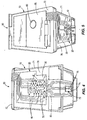
- FIG. 1 illustrates an exemplary print cartridge 70, such as an ink jet print head cartridge.
- the print cartridge 70 includes a first circuit in the form of a cartridge electrical circuit 80.
- the cartridge electrical circuit 80 acts as an electronic interface between a printer controller associated with a printing device (not shown) and the print cartridge 70.
- the cartridge electrical circuit 80 includes a plurality of cartridge contacts 82 that electrically communicate with a plurality of printer contacts (not shown) when the cartridge 70 is installed in a printer.
- the cartridge contacts 82 and printer contacts allow the printer to electrically communicate with the cartridge electrical circuit 80 to perform operational checks, print functions, and the like. While the illustrated example print cartridge 70 uses a flexible circuit, the present teachings may be applied to print cartridges 70 having other circuit configurations.
- the illustrated print cartridge 70 is an ink jet cartridge and includes a housing 71, a cap 72 and an ink jet print head 73.
- the housing 71 includes a cartridge front face 76 to which a portion of the cartridge electrical circuit 80 is secured.
- the illustrated ink jet print head 73 includes an orifice plate 74 and ink jet nozzles 75.
- the illustrated print cartridge 70 further includes a silicon die (not shown) that may be located underneath the orifice plate 74.
- the silicon die and/or the cartridge electrical circuit 80 may include cartridge memory.
- the cartridge electrical circuit 80 may include memory in the form of first embedded memory arrays that are used to store printing parameters. These printing parameters may include any suitable information related to the print cartridge 70, such as production dates, ink container size, ink levels, age of the ink in the print cartridge, regional settings (e.g., United States or Europe) and a cartridge identification number, for example.
- the cartridge contacts 82 also receive signals from the printer for operating the print head 73.
- the cartridge contacts 82 of the illustrated embodiment operate to provide the printer with information about the print cartridge 70 and to receive operating signals from the printer during print operations.
- Other cartridge embodiments may not include an integrated print head 73, in which case the cartridge contacts 82 may operate solely to exchange information signals with the printer to provide the printer with information about the print cartridge 70.
- Each memory location in the first embedded memory arrays may include an electrical switch device, such as an electrical fuse or a field effect transistor (FET), for example.
- an electrical signal may be sent to a particular memory location to program, burn, blow, or damage the electrical switch device, thereby rendering that particular memory location unable to be reset in the case of a one-time programmable memory.
- the memory location that stores the ink level may be programmed (e.g., burned) so that if the print cartridge 70 is refilled with new ink, accurate information cannot be provided to the printer about the ink levels in the print cartridge 70.
- the first embedded memory arrays may be re-programmable or resettable memory arrays.
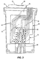
- FIG. 2 illustrates a first embodiment of an electronic patch 10 for attachment to the print cartridge 70.
- Figs. 3-7 illustrate the electronic patch 10 attached to the print cartridge 70 in order to create a refurbished or repaired print cartridge 90.
- Both the used print cartridge 70 and the refurbished print cartridge 90 may be configured to be used in the same printing device, such as a printer (not shown).
- the used print cartridge 70 may be modified during remanufacturing such that the refurbished print cartridge 90 is compatible with a different printer device or devices other than the original use print cartridge 70.
- the electronic patch 10 includes a second circuit in the form of a replacement or patch circuit 20 configured to fit over a portion of the cartridge electrical circuit 80 on the used print cartridge 70.
- the patch circuit 20 includes a substrate 30, which in the illustrated construction comprises a flexible substrate, but which may also be or include a printed circuit board (PCB) substrate, or other suitable circuit substrate.
- the illustrated patch circuit 20 also includes a plurality of lead lines 40, a plurality of contact pads 50 and an integrated control chip 60.
- the patch circuit 20 and/or the integrated control chip 60 may include patch memory, which may be in the form of replacement or second embedded memory arrays.
- the patch substrate 30 may be formed from any suitable material, such as any type of polymer, for example.
- a substrate 30 that is flexible may be configured to flexibly align with the contours of the used print cartridge 70 to which it is attached. For example, a flexible substrate 30 may bend around a corner of the used print cartridge 70 as best shown in FIG. 4 . As discussed further herein, other embodiments may include a substantially rigid substrate.
- the lead lines 40 and the contact pads 50 may be formed from any suitable conductive material, such as gold, copper or platinum, for example.
- the lead lines 40 and the contact pads 50 are configured to convey electrical signals from a printer controller (not shown) to the refurbished print cartridge 90, as well as to convey electrical signals from both the refurbished print cartridge 90 and the integrated control chip 60 to the printer controller.
- the electrical signals may be or include control or data signals for operation or diagnostics of the refurbished print cartridge 90. For example, some electrical signals may be used to control ink jet nozzles 75 in an orifice plate 74 of a refurbished ink jet print cartridge 90 (see FIG. 3 ).
- the integrated control chip 60 may be any suitable electronic control device, such as a microcontroller, an application specific integrated circuit (ASIC) or a field programmable gate array (FPGA), for example.
- the integrated control chip 60 includes or communicates with the patch memory and may provide electrical signals to the printer corresponding to printing parameters such as ink levels, for example.
- the patch memory may be configured similarly to the cartridge memory, and may be provided with "one shot" electrical devices associated with each memory location (e.g., electrical fuse or FET), such that any of the replacement memory locations can be burned or damaged in a similar manner as the first embedded memory array locations of the print cartridge 70.
- the replacement embedded memory arrays may have any suitable multiuse electrical devices that may be switched and/or reset without damage to the memory location, such as resettable fuses or electrically erasable memory, for example.
- the electrical control signal from the printer controller to program e.g., burn
- the multiuse electrical device may switch to an off state, thereby mimicking burning or damaging of the memory location and putting the memory location in a state that is temporarily unable to be reset.
- the multiuse electrical device may be reprogrammed such that the memory location once again stores information relevant to the ink level of the re-refurbished print cartridge.
- the patch circuit 20 is positioned over a portion of the cartridge electrical circuit 80 such that some or all of the contact pads 50 are in contact with contact pads of the underlying cartridge electrical circuit 80.
- Some of the contact pads 50 may be configured as pass-through contacts that allow electrical signals to pass through to or from the electrically controlled elements of the print cartridge 70.
- some contact pads 50 may be in pass-through contact with the underlying contact pads of the cartridge electrical circuit 80 that receive operating signals from the printer to control operation of the print head 73 and ink jet nozzles 75 of the print cartridge 70, thereby allowing the ink jet nozzles 75 of the refurbished print cartridge 90 to be controlled directly by the printer controller without any intervention or interference by the integrated control circuit 60.
- the pass-through contact pads may nonetheless communicate with the integrated control circuit 60 (e.g., via a wire trace 40) to allow the integrated control circuit 60 to monitor communication between the printer and the circuit 80.
- Other pass-through contact pads may not communicate in any manner with the integrated control circuit 60, and may simply function as a conductor for electrical signals between the printer and the circuit 80.
- the pass-through contact pads 50 may transmit operating signals and/or information signals between the printer and the cartridge electrical circuit 80.
- Some contact pads 50 may be aligned with underlying contact pads of the cartridge electrical circuit 80 that are associated with the burned or damaged memory locations of the used print cartridge 70. These contact pads 50 may function as replacement contact pads and may be connected through lead lines 40 to the integrated control chip 60 such that an electrical signal that is intended for the contact pad of the cartridge electrical circuit 80 associated with a disabled memory location is re-routed to an appropriate portion of the integrated control chip 60, such as a replacement embedded memory location. For example, the printer controller may send an information signal in the form of a query regarding the level of ink in the refurbished print cartridge 90 to a contact pad associated with a non-functional memory location.
- the electrical query signal may be re-routed to a corresponding embedded memory location in the integrated control chip 60 in which data corresponding to the current ink level value is stored. Because the integrated control chip 60 provides the printer controller with an appropriate response, the printer continues to function.
- the replacement contact pads 50 of the patch circuit 20 may not be electrically connected with the contact pads associated with the burned or damaged memory locations of the used print cartridge 80 because the burned or damaged memory locations may be at least partially non-functional, making electrical connection therewith unnecessary.
- the patch circuit 20 is a flexible circuit and extends up the front and over onto the top of the used print cartridge 70.
- the integrated control chip 60 is positioned in the portion of the patch circuit 20 that is positioned on top of the used print cartridge 70.
- the integrated control chip 60 may be encased in a protective material, such as a moldable polymer, for example.
- the integrated control chip 60 may be partially or fully encased within the substrate 30.
- the refurbished print cartridge 90 may also include an identification label 95.
- an identification label 95 is positioned on the cap 72 and over the portion of the patch circuit 20 in which the integrated control chip 60 is positioned.
- the label 95 may be provided with a hole 96 that accommodates the protective material surrounding the integrated control chip.
- the patch circuit 20 may be attached to the used print cartridge 70 by any suitable attaching means.
- portions of the substrate 30 may be coated or impregnated with an adhesive.
- portions of the used print cartridge 70 may be coated with an adhesive.
- the contact pads 50 of the electronic patch 10 may include solder material on the side that mates to the corresponding contact pads on the used print cartridge 70, thereby allowing the contact pads 50 to be soldered to the contact pads on the used print cartridge 70.
- Other suitable attaching techniques may include overmolding, adhesive tape, ultrasonic welding, and the like, without limitation.
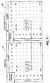
- an embodiment of a printing system 300 includes a printer 310 and a refurbished print cartridge 90.
- the printer 310 includes a driver board 320 and an interconnect board 330.
- the interconnect board 330 is in electrical communication with the driver board 320 and with the cartridge electrical circuit 80 of the print cartridge 70.
- the cartridge electrical circuit 80 is in electrical communication with a memory array 78 of the print cartridge 70 through an address selection section 79.
- the interconnect board 330 and the cartridge electrical circuit 80 are both in electrical communication with the electronic patch 10, which is in electrical communication with the memory array 98 of the electronic patch 10 through an address selection section 99.
- connections between the cartridge electrical circuit 80 and the electronic patch 10 may be pass-through connections that allow unrestricted communication between the printer 310 and the cartridge electrical circuit 80.
- Other connections between the cartridge electrical circuit 80 and the electronic patch may be replacement connections that re-route communications that would otherwise pass between the printer and the cartridge electrical circuit 80 such that those communications pass between the printer and the electronic patch 10.
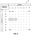
- the print cartridge memory array 78 is illustrated as a two dimensional array of rows and columns where each intersecting location of a row and a column is a specific memory location.
- particular memory locations may be programmed with an electrical signal to program, burn, or damage an electrical device associated with that memory location in order to render that memory location unable to provide accurate information to the printer for a refilled print cartridge.
- the three particular memory locations at the intersections of row R4 and columns C1, C2 and C3 have been burned over the life cycle of the used print cartridge 70 and are no longer able to provide accurate information to the printer about a refilled print cartridge.
- these three memory locations are responsible for storing information regarding the ink levels of the print cartridge, they may provide information to the printer indicating that the print cartridge is empty or defective. This indication will be provided to the printer even if the print cartridge is refilled with printing ink, thereby causing the operation of the printer to stop or be inaccurate.
- the electronic patch memory array 98 is illustrated as a two dimensional array of rows and columns where each intersecting location of a row and a column is a specific memory location. These memory locations are mapped to the corresponding memory locations of the used print cartridge memory array 78. As illustrated in FIG. 10 , the three particular memory locations at the intersections of row R4 and columns C1, C2 and C3 are usable memory locations, which are mapped directly to the corresponding burned memory locations in the used print cartridge memory array 78 as illustrated in FIG. 11 .
- the usable memory locations of the electronic patch memory array 98 render the otherwise non-functional cartridge electrical circuit 80 functional, for example by providing ink level information to the printer.
- the printer controller communicates with electronic patch memory array 98, operational data is returned to the print controller and the printer is allowed to perform print functions.
- This allows a depleted or used print cartridge 70 to be refilled with ink and repaired as a refurbished print cartridge 90 by adding the electronic patch 10, thereby saving on manufacturing costs and waste.
- the refurbished print cartridge 90 may be refurbished yet again by either replacing the electronic patch 10 or by resetting the electrical switch devices in the memory arrays of the electronic patch 10.
- the electronic patch memory array 98 may be configured to reset and/or store any printing parameters, such as the production date, the ink container size, the age of the ink, the regional settings, the cartridge identification number and the ink levels, for example.
- FIG. 12 illustrates a second embodiment of an electronic patch 110.
- Electronic patch 110 includes a replacement circuit 120.
- the replacement circuit 120 includes a substrate 130, a plurality of lead lines 140, a plurality of contact pads 150 and an integrated control chip 160 with replacement or second embedded memory arrays.
- the electronic patch 110 is configured to be positioned entirely on the front face 76 of the used print cartridge 70, and therefore would not extend up the front face 76 and over onto the cap 72 as illustrated in the first embodiment discussed above.
- the electrical functions of the electronic patch 110 may be similar to the electrical functions of the electronic patch 10 discussed above.
- FIG. 13 illustrates a third embodiment of an electronic patch 210.
- Electronic patch 210 includes a replacement circuit 220.
- the replacement circuit 220 includes a substrate 230, a plurality of lead lines 240, a plurality of contact pads 250 and an integrated control chip 260 with replacement or second embedded memory arrays.
- the electronic patch 210 is configured to be positioned entirely on the front face 76 of the used print cartridge 70, and therefore would not extend up the front face 76 and over onto the cap 72 as illustrated in the first embodiment discussed above.
- the electrical functions of the electronic patch 210 may be similar to the electrical functions of the electronic patch 10 discussed above.
- FIG. 1 illustrates a third embodiment of an electronic patch 210.
- FIG. 13 illustrates an embodiment having pass-through contact pads (e.g., pads 250a) that are not in communication with the integrated control chip 260, and replacement contact pads 250b that are in communication with the integrated control chip 260. It should be appreciated, however, that even though a contact pad 250 may have a lead line 240 electrically coupling it to the integrated control chip 260, that contact pad 250 may still function as a pass through contact pad, with the communication afforded by the lead line 240 being provided primarily or exclusively for purposes of monitoring communications between the printer and the cartridge electrical circuit 80.
- pass-through contact pads e.g., pads 250a
- FIGS. 14 and 15 illustrate a fourth embodiment of an electronic patch 410 that includes a rigid substrate 414 having a front side 418 ( FIG. 15 ) and a back side 422 ( FIG. 14 ).
- the front side 418 is configured to face away from the print cartridge to which the electronic patch 410 is attached, and includes a plurality of contact pads 426 arranged for electrical engagement with electrical contacts of the printer into which the print cartridge and electronic patch are installed.
- the back side 422 faces toward and electrically couples with the print cartridge, as discussed further below.
- the back side 422 includes a plurality of solder locations 430 that are opposite and in electrical communication with the contact pads 426 on the front side 418 of the patch 410.
- the back side 422 also includes electrical traces 434 that extend between the solder locations 430 and a variety of circuit components 438.
- the circuit components 438 and traces 434 are also in electrical communication with an integrated control chip 442, which in the illustrated embodiment is encased in a dome of protective polymer material.
- the components provided on the substrate 414 define a replacement circuit 446 that renders an otherwise non-functional used printer cartridge functional, as discussed above.
- the embodiment of FIGS. 14 and 15 includes replacement contact pads and pass through contact pads.
- contact pad 426a illustrates a replacement contact pad that is not electrically connected to the used print cartridge 70. More specifically, by comparing FIGS. 14 and 15 , it can be seen that unlike the other contact pads 426, the replacement contact pad 426a does not have a corresponding solder location 430 for electrically coupling the contact pad 426a with a corresponding cartridge contact 82 on the used print cartridge 70. Although other configurations are possible, in many instances the replacement contact pad 426a is located to correspond with the location of a contact pad 82 on the used printer cartridge 70 associated with a non-functional memory location.
- the electronic patch 410 also includes a plurality (e.g. four, as shown) of programming contact pads 450.
- the programming contact pads 450 communicate with the integrated control chip 442 but do not necessarily communicate with either the printer or the used print cartridge 70.
- the programming contact pads 450 may be used to program or reprogram the electronic patch 410.
- the electronic patch 410 may be programmed to operate with different types of printers or print cartridges, and may be programmed to reset and/or store printing parameters, such as the production date, ink container size, ink type, ink quantity, ink age, regional settings, the cartridge identification number, printer messaging parameters, and the like.
- the patch 410 can be reprogrammed without removing the patch from the print cartridge. In this way, when a print cartridge already having a patch 410 attached thereto is depleted of ink and returned for remanufacturing, the patch 410 can be reprogrammed with appropriate information without removing the patch from the cartridge.
- the patch may be reprogrammed by way of the contact pads 426, 426a, in which case the contact pads 426, 426a also comprise programming contact pads 450.
- FIG. 16 illustrates a used print cartridge 70 that has been modified to accept the electronic patch 410. More specifically, a portion of the front face 76 of the print cartridge 70 has been removed to define a recess 458 sized and positioned to receive the integrated control chip 442 on the back side 422 of the electronic patch 410.
- the recess 458 may be formed in the area above the cartridge contacts 82.
- the recess 458 may be formed using an end mill or other any suitable material removal technique.
- the recess 458 allows the electronic patch 410 to sit substantially level with the front face 76 of the cartridge 70 when the patch 410 is attached to the cartridge 410.
- FIG. 17 illustrates the electronic patch 410 attached to the print cartridge 70 that has been modified with the recess 458.
- the patch contact pads 426, 426a are positioned over respective cartridge contacts 82 and, with the exception of the contact pad 426a, electrically communicate therewith.
- the patch 410 is soldered to the print cartridge 70 by way of the solder locations 430 provided on the back side 422 of the substrate 414.
- the cartridge 70 and the patch 410 may be fixtured such that the solder locations 430 are aligned and in contact with their respective cartridge contacts 82.
- a heated die may then be urged against the patch contact pads 426, 426a, simultaneously applying heat and pressure to the contact pads 426, 426a.
- the contact pads 426, 426a conduct heat from the die to the solder locations 430 until the solder at the solder locations 430 melts and flows over the cartridge contacts 82.
- the heated die can then be removed, allowing the solder to cool and solidify and thereby bonding the patch 410 to the print cartridge 70.
- the solder locations 430 thus electrically and mechanically couple the patch 410 to the cartridge 70.
- the solder locations 430 may be the only mechanism by which the patch 410 is mechanically coupled to the cartridge 70.
- the electronic patch 410 may be programmed to interact with the printer in a way that causes the printer to generate certain messages to the user when a print cartridge carrying the electronic patch 410 is inserted into the printer. Messages to the user may be displayed on an LCD display built into the printer, or may be displayed on a computer monitor associated with the computer from which the user is printing.
- the electronic patch 410 may be programmed to cause the printer to generate a message to the user that indicates that a "Genuine OEM" cartridge has been installed in the printer. In some printer types, a "Genuine OEM” message may be required in order to gain access to all available printer functions, and to eliminate annoying pop-up messages during operation.
- the electronic patch 410 may alternatively be programmed to cause the printer to generate a "used genuine OEM” message, a "non-OEM supply” message, or other messages that are generally defined by firmware residing within the printer controller.
- a used or depleted print cartridge 70 may be refurbished into print cartridge 90 for reuse in a printer.
- the refurbishing process may include cleaning the used print cartridge 70 and refilling the used print cartridge 70 with the appropriate printing ink.
- the refurbishing process may also include positioning and attaching an electronic patch 10, 110, 210, 410 over a portion of the cartridge electrical circuit 80 on the used print cartridge 70, so that the contact pads 50 and solder locations 430 on the replacement circuit 20, 120, 220, 446 are in electrical contact with the appropriate corresponding contact pads 82 of the cartridge electrical circuit 80.
- the refurbishing process may further include positioning and attaching an identification label 95 on the used print cartridge 70.
- the refurbishing process may also include testing the refurbished print cartridge 90 for proper operation.
- the refurbishing process may further include resetting or storing at least one of the production date, the ink container size, the age of the ink, the regional settings, the cartridge identification number and the ink levels.
- the refurbishing process provides for re-using a used print cartridge 70 in which one or more memory arrays are permanently damaged.
- the electronic patch 10, 110, 210, 410 may be used to refurbish a used print cartridge 70 that has resettable or re-programmable memory arrays.
- the electronic patch 10, 110, 210, 410 provides for re-using the used print cartridge 70 without having to reprogram or reset the original memory arrays, but instead provides the same override signals as for a single shot memory array.
- the reprogrammable or resettable memory locations in the used print cartridge 70 that have been programmed to mimic a burned or destroyed memory location are left in that state and the corresponding memory locations in the electronic patch 10, 110, 210, 410 are used to replace these switched off memory locations.
- the electronic patches 10, 110, 210, and 410 may provide remanufacturers with enhanced flexibility for responding to OEM firmware updates.
- electronic patches 410 may be programmed "in line" as part of the manufacturing process, thereby allowing for rapid changes in the programming of the electronic patches 410 in response to OEM firmware updates.
Landscapes
- Engineering & Computer Science (AREA)
- Manufacturing & Machinery (AREA)
- Ink Jet (AREA)
- Accessory Devices And Overall Control Thereof (AREA)
Claims (20)
- Ein elektronischer Patch-Aufbau für die Verwendung auf einer Druckerpatrone (70), wobei die Druckerpatrone einen Patronenschaltkreis (80) mit einer Mehrzahl an in einem Muster angeordneten Patronenkontaktflächen (82) hat, und wobei der elektronische Patch-Aufbau enthält:ein mit der Druckerpatrone (70) verbindbares Substrat (30);ein mit dem Substrat (30) verbundener Patch-Schaltkreis (20); undeine Mehrzahl an auf dem Substrat vorgesehenen Patch-Kontaktflächen (50), wobei zumindest einige der Patch-Kontaktflächen (50) angeordnet sind, um dem Muster zu entsprechen, und wobei die Mehrzahl an Patch-Kontaktflächen (50) eine Durchtrittskontaktfläche, welche es elektrischen Signalen ermöglicht, zum ersten Schaltkreis hindurchzutreten, wenn das Substrat (30) mit der Druckerpatrone (70) verbunden ist, und eine Ersatzkontaktfläche, welche elektrische Signale zum Patch-Schaltkreis (20) leitet, enthält.
- Der elektronische Patch-Aufbau gemäß Anspruch 1, wobei der Patch-Schaltkreis (20) einen mit der Ersatzkontaktfläche verbundenen Speicher enthält.
- Der elektronische Patch-Aufbau gemäß Anspruch 2, wobei der Speicher eine eingebettete Speicheranordnung, die einen nicht funktionierenden mit dem Patronenschaltkreis (80) verbundenen Speicher ersetzt, enthält.
- Der elektronische Patch-Aufbau gemäß Anspruch 2, wobei der Speicher Tintenstandsinformation speichert.
- Der elektronische Patch-Aufbau gemäß Anspruch 1, wobei das Substrat (30) eine Vorderseite, die von der Druckerpatrone (70) abgewandt ist, wenn das Substrat (30) mit der Druckerpatrone verbunden ist, und eine Rückseite, die der Druckerpatrone (70) zugewandt ist, wenn das Substrat (30) mit der Druckerpatrone (70) verbunden ist, enthält, und wobei die Mehrzahl an Patch-Kontaktflächen (50) auf der Vorderseite des Substrats (30) vorgesehen ist.
- Der elektronische Patch-Aufbau gemäß Anspruch 5, ferner enthaltend eine Mehrzahl an Lötstellen, wobei die Lötstellen auf der Rückseite des Substrats (30) vorgesehen sind, wobei die Lötstellen angeordnet sind, um dem Muster zu entsprechen, und wobei jede Lötstelle mit einer entsprechenden der Mehrzahl an Patch-Kontaktflächen (50) in elektrischer Verbindung steht.
- Der elektronische Patch-Aufbau gemäß Anspruch 5, wobei der Patch-Schaltkreis (20) einen Steuerchip (60) enthält, und wobei der Steuerchip an die Rückseite der Druckerpatrone (70) gekoppelt ist.
- Der elektronische Patch-Aufbau gemäß Anspruch 7, wobei der Steuerchip (60) ein Mikrocontroller oder ein anwendungsspezifischer integrierter Schaltkreis (ASIC) oder eine feldprogrammierbare Gatteranordnung (FPGA) ist.
- Der elektronische Patch-Aufbau gemäß Anspruch 1, wobei die Mehrzahl an Patch-Kontaktflächen (50) Programmierkontaktflächen, die in elektrischer Verbindung mit dem Patch-Schaltkreis (20) stehen und dem Muster nicht entsprechen, enthält.
- Ein Druckerpatronenaufbau enthaltend:eine Druckerpatrone (70) enthaltend einen Patronenschaltkreis (80) mit einer Mehrzahl an in einem Muster angeordneten Patronenkontaktflächen (82), wobei der Patronenschaltkreis (80) zumindest ein nicht funktionierendes Schaltelement enthält; undeine elektronische Patch-Anordnung, die an die Patrone (70) gekoppelt ist und mit dem Patronenschaltkreis (80) in elektrischer Verbindung steht, wobei die elektronische Patch-Anordnung enthält:ein an die Druckerpatrone (70) gekoppeltes Substrat (30);eine Mehrzahl an auf dem Substrat (30) vorgesehenen Patch-Kontaktflächen (50), wobei zumindest einige der Patch-Kontaktflächen (50) angeordnet sind, um dem Muster zu entsprechen, und in elektrischer Verbindung mit einer entsprechenden der Patronenkontaktflächen (82) stehen; undein Patch-Schaltkreis (20), der an das Substrat (30) gekoppelt ist und mit zumindest einigen von der Mehrzahl an Patch-Kontaktflächen (50) in elektrischer Verbindung steht, wobei der Patch-Schaltkreis (20) ein Ersatzschaltelement zum Ersetzen des nicht funktionierenden Schaltelements des Patronenschaltkreises (80) enthält.
- Der Druckerpatronenaufbau gemäß Anspruch 10, wobei das nicht funktionierende Schaltelement einen Speicherplatz einer ersten eingebetteten Speicheranordnung des Patronenspeichers (80) enthält, und wobei das Ersatzschaltelement einen Speicherplatz einer zweiten eingebetteten Speicheranordnung des Patch-Schaltkreises (20) enthält.
- Der Druckerpatronenaufbau gemäß Anspruch 10, wobei die zweite eingebettete Speicheranordnung eingerichtet ist, um Information, die sich auf das Herstellungsdatum und/oder die Größe des Tintentanks und/oder das Alter der Tinte und/oder die Regionseinstellungen und/oder die Patronenidentifikationsnummer und/oder die Tintenstände bezieht, zu speichern.
- Der Druckerpatronenaufbau gemäß Anspruch 10, wobei die Mehrzahl an Patch-Kontaktflächen (50) eine Durchtrittskontaktfläche, welche es elektrischen Signalen ermöglicht, durch den elektronischen Patch-Aufbau zum Patronenschaltkreis (80) ohne Unterbrechung hindurchzutreten, und eine Ersatzkontaktfläche, welche elektrische Signale zum Ersatzschaltelement leitet, enthält.
- Der Druckerpatronenaufbau gemäß Anspruch 13, wobei das Substrat (30) eine Vorderseite, die von der Druckerpatrone (70) abgewandt ist, und eine Rückseite, die der Druckerpatrone (70) zugewandt ist, enthält, wobei die Mehrzahl an Patch-Kontaktflächen (50) auf der Vorderseite des Substrats (30) ist, wobei der elektronische Patch-Aufbau ferner eine Mehrzahl an auf der Rückseite des Substrats (30) vorgesehenen Lötstellen enthält, wobei jede Lötstelle gegenüber einer entsprechenden der Mehrzahl an Patch-Kontaktflächen (50) angeordnet und mit einer entsprechenden der Mehrzahl an Patronenkontaktflächen (82) verbunden ist.
- Der Druckerpatronenaufbau gemäß Anspruch 14, wobei die Druckerpatrone (70) eine Vorderseite, mit der der elektronische Patch-Aufbau verbunden ist, enthält, wobei die Vorderseite eine in ihr gebildete Vertiefung hat und wobei die Vertiefung einen Teil des Patch-Schaltkreises (20) aufnimmt.
- Der Druckerpatronenaufbau gemäß Anspruch 13, wobei die Mehrzahl an Patronenkontaktflächen (82) eine Patronenkontaktfläche zum Empfangen von Betriebssignalen und eine Patronenkontaktfläche zum Empfangen von Informationssignalen enthält, wobei die Durchtrittskontaktfläche in elektrischer Verbindung mit der Patronenkontaktfläche (82) zum Empfangen von Betriebssignalen steht, und wobei die Ersatzkontaktfläche in elektrischer Verbindung mit der Patronenkontaktfläche (82) zum Empfangen von Informationssignalen steht.
- Der Druckerpatronenaufbau gemäß Anspruch 10, wobei die Druckerpatrone (70) eine gebrauchte Druckerpatrone und der Druckerpatronenaufbau eine instandgesetzte Druckerpatrone ist.
- Ein Druckerpatronenaufbau enthaltend:eine gebrauchte Druckerpatrone (70), die eine Vorderseite hat und einen Patronenschaltkreis (80) mit einer Mehrzahl an Patronenkontaktflächen (82) enthält, wobei der Patronenschaltkreis (80) zumindest ein nicht funktionierendes Schaltelement enthält, und die Vorderseite eine in ihr gebildete Vertiefung hat; undeine elektronische Patch-Anordnung, die an die Patrone gekoppelt ist und mit dem Patronenschaltkreis (80) in elektrischer Verbindung steht, wobei die elektronische Patch-Anordnung enthält:ein an die Vorderseite der Druckerpatrone (70) gekoppeltes Substrat (30), wobei das Substrat (30) eine Vorderseite, die von der Druckerpatrone (70) abgewandt ist, und eine Rückseite, die der Druckerpatrone (70) zugewandt ist, hat;ein Patch-Schaltkreis (20) enthaltend einen Steuerchip (60) und ein Ersatzschaltelement zum Ersetzen des nicht funktionierenden Schaltelements des Patronenschaltkreises (80), wobei sich der Steuerchip (60) von der Rückseite des Substrats (30) erstreckt und in der Vertiefung aufgenommen ist;eine Mehrzahl an auf der Vorderseite des Substrats (30) vorgesehenen Patch-Kontaktflächen (50), wobei zumindest einige der Patch-Kontaktflächen (50) in elektrischer Verbindung mit dem Patronenschaltkreis (20) stehen; undeine Mehrzahl an auf der Rückseite des Substrats (30) vorgesehenen Lötstellen, wobei jede Lötstelle in elektrischer Verbindung mit einer entsprechenden der Patch-Kontaktflächen (50) steht und ferner elektrisch und mechanisch mit einer entsprechenden der Patronenkontaktflächen (82) verbunden ist, wodurch bestimmte der Patronenkontaktflächen (82) mit den entsprechenden Patch-Kontaktflächen (50) elektrisch verbunden werden, wobei die Mehrzahl an Patch-Kontaktflächen (50) zumindest eine Durchtrittskontaktfläche, welche es elektrischen Signalen ermöglicht, durch den elektronischen Patch-Aufbau zum Patronenschaltkreis (80) ohne Unterbrechung hindurchzutreten, und zumindest eine Ersatzkontaktfläche, welche elektrische Signale zum Ersatzschaltelement leitet, enthält.
- Der Druckerpatronenaufbau gemäß Anspruch 18, wobei die Mehrzahl an Patronenkontaktflächen (82) eine Patronenkontaktfläche zum Empfangen von Betriebssignalen und eine Patronenkontaktfläche zum Empfangen von Informationssignalen enthält, wobei die zumindest eine Durchtrittskontaktfläche in elektrischer Verbindung mit der Patronenkontaktfläche (82) zum Empfangen von Betriebssignalen steht und wobei die zumindest eine Ersatzkontaktfläche in elektrischer Verbindung mit der Patronenkontaktfläche (82) zum Empfangen von Informationssignalen steht.
- Der Druckerpatronenaufbau gemäß Anspruch 18, wobei das nicht funktionierende Schaltelement einen Speicherplatz einer ersten eingebetteten Speicheranordnung des Patronenspeichers (80) enthält, und wobei das Ersatzschaltelement einen Speicherplatz einer zweiten eingebetteten Speicheranordnung des Patch-Schaltkreises (20) enthält.
Priority Applications (2)
| Application Number | Priority Date | Filing Date | Title |
|---|---|---|---|
| EP17211172.6A EP3403830B1 (de) | 2013-02-12 | 2014-02-06 | Elektronisches pflaster zur aufarbeitung einer gebrauchten druckpatrone |
| EP16182741.5A EP3115214B1 (de) | 2013-02-12 | 2014-02-06 | Elektronisches pflaster zur wiederherstellung einer gebrauchten druckpatrone |
Applications Claiming Priority (2)
| Application Number | Priority Date | Filing Date | Title |
|---|---|---|---|
| US201361763589P | 2013-02-12 | 2013-02-12 | |
| PCT/US2014/015046 WO2014126775A1 (en) | 2013-02-12 | 2014-02-06 | Electronic patch for refurbishing a used print cartridge |
Related Child Applications (2)
| Application Number | Title | Priority Date | Filing Date |
|---|---|---|---|
| EP17211172.6A Division EP3403830B1 (de) | 2013-02-12 | 2014-02-06 | Elektronisches pflaster zur aufarbeitung einer gebrauchten druckpatrone |
| EP16182741.5A Division EP3115214B1 (de) | 2013-02-12 | 2014-02-06 | Elektronisches pflaster zur wiederherstellung einer gebrauchten druckpatrone |
Publications (2)
| Publication Number | Publication Date |
|---|---|
| EP2956308A1 EP2956308A1 (de) | 2015-12-23 |
| EP2956308B1 true EP2956308B1 (de) | 2016-08-17 |
Family
ID=50151401
Family Applications (3)
| Application Number | Title | Priority Date | Filing Date |
|---|---|---|---|
| EP17211172.6A Active EP3403830B1 (de) | 2013-02-12 | 2014-02-06 | Elektronisches pflaster zur aufarbeitung einer gebrauchten druckpatrone |
| EP14705935.6A Not-in-force EP2956308B1 (de) | 2013-02-12 | 2014-02-06 | Elektronisches pflaster zur wiederherstellung einer gebrauchten druckpatrone |
| EP16182741.5A Not-in-force EP3115214B1 (de) | 2013-02-12 | 2014-02-06 | Elektronisches pflaster zur wiederherstellung einer gebrauchten druckpatrone |
Family Applications Before (1)
| Application Number | Title | Priority Date | Filing Date |
|---|---|---|---|
| EP17211172.6A Active EP3403830B1 (de) | 2013-02-12 | 2014-02-06 | Elektronisches pflaster zur aufarbeitung einer gebrauchten druckpatrone |
Family Applications After (1)
| Application Number | Title | Priority Date | Filing Date |
|---|---|---|---|
| EP16182741.5A Not-in-force EP3115214B1 (de) | 2013-02-12 | 2014-02-06 | Elektronisches pflaster zur wiederherstellung einer gebrauchten druckpatrone |
Country Status (4)
| Country | Link |
|---|---|
| US (3) | US9421783B2 (de) |
| EP (3) | EP3403830B1 (de) |
| ES (2) | ES2663550T3 (de) |
| WO (1) | WO2014126775A1 (de) |
Families Citing this family (20)
| Publication number | Priority date | Publication date | Assignee | Title |
|---|---|---|---|---|
| US9579198B2 (en) | 2012-03-01 | 2017-02-28 | Twelve, Inc. | Hydraulic delivery systems for prosthetic heart valve devices and associated methods |
| US9421783B2 (en) | 2013-02-12 | 2016-08-23 | Clover Technologies Group, Llc | Electronic patch for refurbishing a used print cartridge |
| CN108292197B (zh) | 2015-11-05 | 2021-06-25 | 惠普发展公司有限责任合伙企业 | 打印机机队内打印剂墨盒的先前安装的确定 |
| DE102016107890B4 (de) * | 2016-04-28 | 2025-09-04 | Oliver Ott | Kontaktfolie und Trägervorrichtung mit einer Kontaktfolie sowie ein Verfahren zu deren Herstellung |
| CN107953677B (zh) * | 2016-12-20 | 2023-11-14 | 极海微电子股份有限公司 | 用于与附属于成像盒的电路板共同使用的电子芯片、成像盒及修复成像盒方法 |
| EP3363637B1 (de) * | 2016-12-22 | 2020-05-13 | Apex Microelectronics Co., Ltd | Regenerativer chip und kontaktsteuerungsverfahren dafür |
| US20190368911A1 (en) * | 2017-03-14 | 2019-12-05 | Hewlett-Packard Development Company, L.P. | Liquid level sensor circuit |
| US10575950B2 (en) | 2017-04-18 | 2020-03-03 | Twelve, Inc. | Hydraulic systems for delivering prosthetic heart valve devices and associated methods |
| US10646338B2 (en) | 2017-06-02 | 2020-05-12 | Twelve, Inc. | Delivery systems with telescoping capsules for deploying prosthetic heart valve devices and associated methods |
| CN107945045B (zh) * | 2017-11-29 | 2021-12-21 | 沈阳工业大学 | 一种基于粒子群遗传算法的再制造装配过程的选配方法 |
| CN109910439A (zh) * | 2017-12-12 | 2019-06-21 | 上海坚芯电子科技有限公司 | 一种电子贴片装置、再制造墨盒及打印机 |
| KR101897057B1 (ko) * | 2018-03-21 | 2018-09-10 | 손방용 | 잉크카트리지 재생용 컨트롤러가 실장된 fpcb |
| US11163245B2 (en) * | 2018-04-30 | 2021-11-02 | Hewlett-Packard Development Company, L.P. | Embedded memory resources |
| CN109572222B (zh) * | 2018-10-23 | 2020-02-14 | 珠海艾派克微电子有限公司 | 再生墨盒、电子补丁及再生墨盒形成方法 |
| JP7427367B2 (ja) | 2019-04-26 | 2024-02-05 | キヤノン株式会社 | 液体吐出ヘッドおよびその製造方法 |
| CN110027324A (zh) * | 2019-05-06 | 2019-07-19 | 珠海艾派克微电子有限公司 | 喷嘴墨盒、喷墨组件及电路基板 |
| CN110103591B (zh) * | 2019-06-13 | 2020-03-27 | 杭州旗捷科技有限公司 | 耗材芯片的自动复位方法、耗材芯片 |
| CN211942586U (zh) * | 2019-12-13 | 2020-11-17 | 杭州旗捷科技有限公司 | 修复芯片、墨盒和打印机 |
| CN214215199U (zh) * | 2020-09-11 | 2021-09-17 | 珠海纳思达企业管理有限公司 | 带有打印头的墨盒 |
| CN112793308B (zh) * | 2021-01-26 | 2021-12-31 | 北海绩迅电子科技有限公司 | 墨囊组件及墨盒 |
Citations (3)
| Publication number | Priority date | Publication date | Assignee | Title |
|---|---|---|---|---|
| EP1201441A1 (de) | 1998-03-04 | 2002-05-02 | Hewlett-Packard Company | Tintenbehälternachfüllsystem |
| WO2005081072A1 (en) | 2004-02-18 | 2005-09-01 | Static Control Components, Inc. | System and method for adjusting toner consumption |
| CN201208811Y (zh) | 2008-06-19 | 2009-03-18 | 珠海纳思达电子科技有限公司 | 一种用于喷墨打印机墨盒上的简单芯片及使用该芯片的墨盒 |
Family Cites Families (41)
| Publication number | Priority date | Publication date | Assignee | Title |
|---|---|---|---|---|
| US5345315A (en) | 1988-11-23 | 1994-09-06 | Imatec, Ltd. | Method and system for improved tone and color reproduction of electronic image on hard copy using a closed loop control |
| US7008050B2 (en) * | 1995-04-27 | 2006-03-07 | Hewlett-Packard Development Company, L.P. | Ink container refurbishment system |
| US5851644A (en) | 1995-08-01 | 1998-12-22 | Loctite (Ireland) Limited | Films and coatings having anisotropic conductive pathways therein |
| US6402876B1 (en) | 1997-08-01 | 2002-06-11 | Loctite (R&D) Ireland | Method of forming a monolayer of particles, and products formed thereby |
| US6325475B1 (en) | 1996-09-06 | 2001-12-04 | Microfab Technologies Inc. | Devices for presenting airborne materials to the nose |
| US6565181B2 (en) | 1997-07-12 | 2003-05-20 | Silverbrook Research Pty Ltd | Printing cartridge with switch array identification |
| AUPO798697A0 (en) | 1997-07-15 | 1997-08-07 | Silverbrook Research Pty Ltd | Data processing method and apparatus (ART51) |
| US6161915A (en) | 1998-06-19 | 2000-12-19 | Lexmark International, Inc | Identification of thermal inkjet printer cartridges |
| US6658219B1 (en) | 1999-09-30 | 2003-12-02 | Fuji Photo Film Co., Ltd. | Method, device, system and recording medium for detecting improper cartridge, and cartridge |
| US7640181B2 (en) | 2000-02-17 | 2009-12-29 | Hart Intercivic, Inc. | Distributed network voting system |
| US6379876B1 (en) | 2000-06-13 | 2002-04-30 | Eastman Kodak Company | Thermally processable imaging element comprising an ion exchanged reducing agent |
| GB2354202B (en) | 2000-08-07 | 2002-09-18 | Dynamic Cassette Int | A printer cartridge kit and method |
| CA2379725C (en) | 2001-04-03 | 2007-06-12 | Seiko Epson Corporation | Ink cartridge |
| HK1080042B (zh) | 2001-07-11 | 2011-07-29 | 洛桑聚合联合学院 | 结合有微结构的图像 |
| US6509126B1 (en) | 2001-12-28 | 2003-01-21 | Eastman Kodak Company | Photothermographic element comprising a fluorescent dye and methods of image formation |
| US8171567B1 (en) | 2002-09-04 | 2012-05-01 | Tracer Detection Technology Corp. | Authentication method and system |
| US7175089B2 (en) | 2003-04-07 | 2007-02-13 | Silverbrook Research Pty Ltd | Face determination |
| US6882810B2 (en) | 2003-08-15 | 2005-04-19 | Static Control Components, Inc. | Method and apparatus for repairing and electronic circuit in a remanufactured replaceable consumable |
| US20050036801A1 (en) * | 2003-08-15 | 2005-02-17 | Static Control Components | Casing for an electronic circuit |
| US7875463B2 (en) | 2004-03-26 | 2011-01-25 | Agilent Technologies, Inc. | Generalized pulse jet ejection head control model |
| US7088928B2 (en) | 2004-08-13 | 2006-08-08 | Static Control Components, Inc. | Systems and methods for universal imaging components |
| US20060053030A1 (en) | 2004-09-07 | 2006-03-09 | Hiroto Nakamura | Method of recycling a liquid cartridge |
| US7328974B2 (en) | 2005-09-29 | 2008-02-12 | Alex Kuo-Shen Wang | Inkjet printer ink cartridge |
| US7424245B2 (en) * | 2005-10-19 | 2008-09-09 | Static Control Components, Inc. | Systems and methods for remanufacturing imaging components |
| KR20070069794A (ko) | 2005-12-28 | 2007-07-03 | 주식회사 파캔오피씨 | 카트리지 재생용 마이크로칩 및 카트리지 재생방법 |
| CN2931121Y (zh) | 2006-05-09 | 2007-08-08 | 聂瑞权 | 喷墨打印机墨盒芯片固定装置 |
| US7515837B2 (en) | 2007-01-17 | 2009-04-07 | Static Control Components, Inc. | System and methods for universal imaging components |
| US8262201B2 (en) | 2007-04-10 | 2012-09-11 | Hewlett-Packard Development Company, L.P. | Micro writing and reading |
| US20080253799A1 (en) | 2007-04-10 | 2008-10-16 | Static Control Components, Inc. | Method for converting a non-chipped imaging cartridge to a multi-use chipped imaging cartridge |
| US20090058958A1 (en) * | 2007-08-27 | 2009-03-05 | Alex Kuo-Shen Wang | Environmental protection ink cartridge / toner cartridge automatic refill chip |
| US20090153602A1 (en) * | 2007-12-18 | 2009-06-18 | Thomas Daniel Brown | Printing Cartridge Refill Method And Associated Cartridge Refill System |
| KR20090085981A (ko) | 2008-02-05 | 2009-08-10 | 삼성전자주식회사 | 잉크카트리지, 화상형성장치 및 잉크카트리지 제조방법 |
| JP5131463B2 (ja) | 2008-03-13 | 2013-01-30 | セイコーエプソン株式会社 | 電子機器システム及び電子機器システムにおける制御方法 |
| US7971947B2 (en) | 2008-04-07 | 2011-07-05 | Static Control Components, Inc. | Systems and methods for remanufacturing imaging components |
| US20090315734A1 (en) | 2008-06-23 | 2009-12-24 | Silverbrook Research Pty Ltd | Electronic pen with automatically retractable nib |
| US8061826B2 (en) | 2008-07-31 | 2011-11-22 | Static Control Components, Inc. | Methods and devices for remanufacturing an imaging cartridge |
| US8160473B2 (en) | 2008-12-08 | 2012-04-17 | Static Control Components, Inc. | Imaging apparatus and methods |
| CN101907859B (zh) * | 2009-08-11 | 2012-01-18 | 珠海天威技术开发有限公司 | 芯片及耗材余量数据更新方法 |
| US20110085310A1 (en) | 2009-10-09 | 2011-04-14 | Cachia Joseph M | Space saving circuit board |
| US8554090B2 (en) | 2009-10-30 | 2013-10-08 | Ui Technologies, Inc. | Replacement printer cartridge chip with a microcontroller with an encrypted memory device |
| US9421783B2 (en) | 2013-02-12 | 2016-08-23 | Clover Technologies Group, Llc | Electronic patch for refurbishing a used print cartridge |
-
2014
- 2014-02-06 US US14/174,056 patent/US9421783B2/en active Active
- 2014-02-06 ES ES16182741.5T patent/ES2663550T3/es active Active
- 2014-02-06 EP EP17211172.6A patent/EP3403830B1/de active Active
- 2014-02-06 ES ES14705935.6T patent/ES2599910T3/es active Active
- 2014-02-06 WO PCT/US2014/015046 patent/WO2014126775A1/en not_active Ceased
- 2014-02-06 EP EP14705935.6A patent/EP2956308B1/de not_active Not-in-force
- 2014-02-06 EP EP16182741.5A patent/EP3115214B1/de not_active Not-in-force
-
2016
- 2016-08-05 US US15/229,306 patent/US9573378B2/en active Active
-
2017
- 2017-01-17 US US15/407,629 patent/US10232630B2/en active Active
Patent Citations (3)
| Publication number | Priority date | Publication date | Assignee | Title |
|---|---|---|---|---|
| EP1201441A1 (de) | 1998-03-04 | 2002-05-02 | Hewlett-Packard Company | Tintenbehälternachfüllsystem |
| WO2005081072A1 (en) | 2004-02-18 | 2005-09-01 | Static Control Components, Inc. | System and method for adjusting toner consumption |
| CN201208811Y (zh) | 2008-06-19 | 2009-03-18 | 珠海纳思达电子科技有限公司 | 一种用于喷墨打印机墨盒上的简单芯片及使用该芯片的墨盒 |
Also Published As
| Publication number | Publication date |
|---|---|
| US9421783B2 (en) | 2016-08-23 |
| US10232630B2 (en) | 2019-03-19 |
| ES2599910T3 (es) | 2017-02-06 |
| EP2956308A1 (de) | 2015-12-23 |
| ES2663550T3 (es) | 2018-04-13 |
| EP3403830A1 (de) | 2018-11-21 |
| EP3115214B1 (de) | 2018-01-03 |
| US20160339712A1 (en) | 2016-11-24 |
| WO2014126775A1 (en) | 2014-08-21 |
| US9573378B2 (en) | 2017-02-21 |
| EP3403830B1 (de) | 2019-11-06 |
| US20170120611A1 (en) | 2017-05-04 |
| HK1232188A1 (en) | 2018-01-05 |
| US20140225946A1 (en) | 2014-08-14 |
| EP3115214A1 (de) | 2017-01-11 |
Similar Documents
| Publication | Publication Date | Title |
|---|---|---|
| EP2956308B1 (de) | Elektronisches pflaster zur wiederherstellung einer gebrauchten druckpatrone | |
| CN104070824B (zh) | 一种带喷头墨盒及其修复方法、喷墨成像设备 | |
| JP4047328B2 (ja) | 液体収納容器、該容器を用いる液体供給システムおよび記録装置、並びに前記容器用回路基板 | |
| RU2295754C2 (ru) | Надежная битовая схема для запоминающего устройства сменного компонента принтера | |
| US7914135B2 (en) | Liquid cartridge and circuit board | |
| CN204472118U (zh) | 修复芯片、墨盒和打印机 | |
| JP6380970B2 (ja) | インクカートリッジ及びチップ | |
| CN207549746U (zh) | 一种电子贴片装置、再制造墨盒及打印机 | |
| US7957655B2 (en) | Systems and methods for imaging components | |
| JP4756928B2 (ja) | プリンタ | |
| HK1232188B (en) | Electronic patch for refurbishing a used print cartridge | |
| JP7714951B2 (ja) | メモリー、カートリッジ、および、印刷システム | |
| TWI710474B (zh) | 重置晶片單元 | |
| JP6427608B2 (ja) | インクカートリッジ及びチップ | |
| JP5767604B2 (ja) | 記録装置及びインク収納容器 | |
| CN121062355A (zh) | 贴片电路的控制方法、贴片电路和再生墨盒 | |
| JP2009126164A (ja) | 液体供給システム、液体消費システム、液体供給装置、ノイズ判定方法 |
Legal Events
| Date | Code | Title | Description |
|---|---|---|---|
| PUAI | Public reference made under article 153(3) epc to a published international application that has entered the european phase |
Free format text: ORIGINAL CODE: 0009012 |
|
| 17P | Request for examination filed |
Effective date: 20150724 |
|
| AK | Designated contracting states |
Kind code of ref document: A1 Designated state(s): AL AT BE BG CH CY CZ DE DK EE ES FI FR GB GR HR HU IE IS IT LI LT LU LV MC MK MT NL NO PL PT RO RS SE SI SK SM TR |
|
| AX | Request for extension of the european patent |
Extension state: BA ME |
|
| GRAP | Despatch of communication of intention to grant a patent |
Free format text: ORIGINAL CODE: EPIDOSNIGR1 |
|
| GRAS | Grant fee paid |
Free format text: ORIGINAL CODE: EPIDOSNIGR3 |
|
| DAX | Request for extension of the european patent (deleted) | ||
| INTG | Intention to grant announced |
Effective date: 20160331 |
|
| GRAA | (expected) grant |
Free format text: ORIGINAL CODE: 0009210 |
|
| AK | Designated contracting states |
Kind code of ref document: B1 Designated state(s): AL AT BE BG CH CY CZ DE DK EE ES FI FR GB GR HR HU IE IS IT LI LT LU LV MC MK MT NL NO PL PT RO RS SE SI SK SM TR |
|
| REG | Reference to a national code |
Ref country code: GB Ref legal event code: FG4D |
|
| REG | Reference to a national code |
Ref country code: CH Ref legal event code: EP |
|
| REG | Reference to a national code |
Ref country code: IE Ref legal event code: FG4D |
|
| REG | Reference to a national code |
Ref country code: AT Ref legal event code: REF Ref document number: 820660 Country of ref document: AT Kind code of ref document: T Effective date: 20160915 |
|
| REG | Reference to a national code |
Ref country code: DE Ref legal event code: R096 Ref document number: 602014003128 Country of ref document: DE |
|
| REG | Reference to a national code |
Ref country code: NL Ref legal event code: MP Effective date: 20160817 |
|
| REG | Reference to a national code |
Ref country code: LT Ref legal event code: MG4D |
|
| REG | Reference to a national code |
Ref country code: AT Ref legal event code: MK05 Ref document number: 820660 Country of ref document: AT Kind code of ref document: T Effective date: 20160817 |
|
| PG25 | Lapsed in a contracting state [announced via postgrant information from national office to epo] |
Ref country code: LT Free format text: LAPSE BECAUSE OF FAILURE TO SUBMIT A TRANSLATION OF THE DESCRIPTION OR TO PAY THE FEE WITHIN THE PRESCRIBED TIME-LIMIT Effective date: 20160817 Ref country code: NL Free format text: LAPSE BECAUSE OF FAILURE TO SUBMIT A TRANSLATION OF THE DESCRIPTION OR TO PAY THE FEE WITHIN THE PRESCRIBED TIME-LIMIT Effective date: 20160817 Ref country code: RS Free format text: LAPSE BECAUSE OF FAILURE TO SUBMIT A TRANSLATION OF THE DESCRIPTION OR TO PAY THE FEE WITHIN THE PRESCRIBED TIME-LIMIT Effective date: 20160817 Ref country code: HR Free format text: LAPSE BECAUSE OF FAILURE TO SUBMIT A TRANSLATION OF THE DESCRIPTION OR TO PAY THE FEE WITHIN THE PRESCRIBED TIME-LIMIT Effective date: 20160817 Ref country code: FI Free format text: LAPSE BECAUSE OF FAILURE TO SUBMIT A TRANSLATION OF THE DESCRIPTION OR TO PAY THE FEE WITHIN THE PRESCRIBED TIME-LIMIT Effective date: 20160817 Ref country code: NO Free format text: LAPSE BECAUSE OF FAILURE TO SUBMIT A TRANSLATION OF THE DESCRIPTION OR TO PAY THE FEE WITHIN THE PRESCRIBED TIME-LIMIT Effective date: 20161117 |
|
| REG | Reference to a national code |
Ref country code: ES Ref legal event code: FG2A Ref document number: 2599910 Country of ref document: ES Kind code of ref document: T3 Effective date: 20170206 |
|
| REG | Reference to a national code |
Ref country code: FR Ref legal event code: PLFP Year of fee payment: 4 |
|
| PG25 | Lapsed in a contracting state [announced via postgrant information from national office to epo] |
Ref country code: GR Free format text: LAPSE BECAUSE OF FAILURE TO SUBMIT A TRANSLATION OF THE DESCRIPTION OR TO PAY THE FEE WITHIN THE PRESCRIBED TIME-LIMIT Effective date: 20161118 Ref country code: PT Free format text: LAPSE BECAUSE OF FAILURE TO SUBMIT A TRANSLATION OF THE DESCRIPTION OR TO PAY THE FEE WITHIN THE PRESCRIBED TIME-LIMIT Effective date: 20161219 Ref country code: LV Free format text: LAPSE BECAUSE OF FAILURE TO SUBMIT A TRANSLATION OF THE DESCRIPTION OR TO PAY THE FEE WITHIN THE PRESCRIBED TIME-LIMIT Effective date: 20160817 Ref country code: AT Free format text: LAPSE BECAUSE OF FAILURE TO SUBMIT A TRANSLATION OF THE DESCRIPTION OR TO PAY THE FEE WITHIN THE PRESCRIBED TIME-LIMIT Effective date: 20160817 Ref country code: PL Free format text: LAPSE BECAUSE OF FAILURE TO SUBMIT A TRANSLATION OF THE DESCRIPTION OR TO PAY THE FEE WITHIN THE PRESCRIBED TIME-LIMIT Effective date: 20160817 Ref country code: SE Free format text: LAPSE BECAUSE OF FAILURE TO SUBMIT A TRANSLATION OF THE DESCRIPTION OR TO PAY THE FEE WITHIN THE PRESCRIBED TIME-LIMIT Effective date: 20160817 |
|
| PG25 | Lapsed in a contracting state [announced via postgrant information from national office to epo] |
Ref country code: RO Free format text: LAPSE BECAUSE OF FAILURE TO SUBMIT A TRANSLATION OF THE DESCRIPTION OR TO PAY THE FEE WITHIN THE PRESCRIBED TIME-LIMIT Effective date: 20160817 Ref country code: EE Free format text: LAPSE BECAUSE OF FAILURE TO SUBMIT A TRANSLATION OF THE DESCRIPTION OR TO PAY THE FEE WITHIN THE PRESCRIBED TIME-LIMIT Effective date: 20160817 |
|
| REG | Reference to a national code |
Ref country code: DE Ref legal event code: R026 Ref document number: 602014003128 Country of ref document: DE |
|
| PLBI | Opposition filed |
Free format text: ORIGINAL CODE: 0009260 |
|
| PG25 | Lapsed in a contracting state [announced via postgrant information from national office to epo] |
Ref country code: CZ Free format text: LAPSE BECAUSE OF FAILURE TO SUBMIT A TRANSLATION OF THE DESCRIPTION OR TO PAY THE FEE WITHIN THE PRESCRIBED TIME-LIMIT Effective date: 20160817 Ref country code: BE Free format text: LAPSE BECAUSE OF FAILURE TO SUBMIT A TRANSLATION OF THE DESCRIPTION OR TO PAY THE FEE WITHIN THE PRESCRIBED TIME-LIMIT Effective date: 20160817 Ref country code: DK Free format text: LAPSE BECAUSE OF FAILURE TO SUBMIT A TRANSLATION OF THE DESCRIPTION OR TO PAY THE FEE WITHIN THE PRESCRIBED TIME-LIMIT Effective date: 20160817 Ref country code: SM Free format text: LAPSE BECAUSE OF FAILURE TO SUBMIT A TRANSLATION OF THE DESCRIPTION OR TO PAY THE FEE WITHIN THE PRESCRIBED TIME-LIMIT Effective date: 20160817 Ref country code: BG Free format text: LAPSE BECAUSE OF FAILURE TO SUBMIT A TRANSLATION OF THE DESCRIPTION OR TO PAY THE FEE WITHIN THE PRESCRIBED TIME-LIMIT Effective date: 20161117 Ref country code: SK Free format text: LAPSE BECAUSE OF FAILURE TO SUBMIT A TRANSLATION OF THE DESCRIPTION OR TO PAY THE FEE WITHIN THE PRESCRIBED TIME-LIMIT Effective date: 20160817 |
|
| PLAX | Notice of opposition and request to file observation + time limit sent |
Free format text: ORIGINAL CODE: EPIDOSNOBS2 |
|
| 26 | Opposition filed |
Opponent name: LUDWIG, GABRIELE Effective date: 20170516 |
|
| PG25 | Lapsed in a contracting state [announced via postgrant information from national office to epo] |
Ref country code: SI Free format text: LAPSE BECAUSE OF FAILURE TO SUBMIT A TRANSLATION OF THE DESCRIPTION OR TO PAY THE FEE WITHIN THE PRESCRIBED TIME-LIMIT Effective date: 20160817 |
|
| PLBB | Reply of patent proprietor to notice(s) of opposition received |
Free format text: ORIGINAL CODE: EPIDOSNOBS3 |
|
| PG25 | Lapsed in a contracting state [announced via postgrant information from national office to epo] |
Ref country code: MC Free format text: LAPSE BECAUSE OF FAILURE TO SUBMIT A TRANSLATION OF THE DESCRIPTION OR TO PAY THE FEE WITHIN THE PRESCRIBED TIME-LIMIT Effective date: 20160817 |
|
| REG | Reference to a national code |
Ref country code: CH Ref legal event code: PL |
|
| PG25 | Lapsed in a contracting state [announced via postgrant information from national office to epo] |
Ref country code: LI Free format text: LAPSE BECAUSE OF NON-PAYMENT OF DUE FEES Effective date: 20170228 Ref country code: CH Free format text: LAPSE BECAUSE OF NON-PAYMENT OF DUE FEES Effective date: 20170228 |
|
| REG | Reference to a national code |
Ref country code: IE Ref legal event code: MM4A |
|
| PG25 | Lapsed in a contracting state [announced via postgrant information from national office to epo] |
Ref country code: LU Free format text: LAPSE BECAUSE OF NON-PAYMENT OF DUE FEES Effective date: 20170206 |
|
| PLBP | Opposition withdrawn |
Free format text: ORIGINAL CODE: 0009264 |
|
| PLBD | Termination of opposition procedure: decision despatched |
Free format text: ORIGINAL CODE: EPIDOSNOPC1 |
|
| REG | Reference to a national code |
Ref country code: FR Ref legal event code: PLFP Year of fee payment: 5 |
|
| PG25 | Lapsed in a contracting state [announced via postgrant information from national office to epo] |
Ref country code: IE Free format text: LAPSE BECAUSE OF NON-PAYMENT OF DUE FEES Effective date: 20170206 |
|
| REG | Reference to a national code |
Ref country code: DE Ref legal event code: R100 Ref document number: 602014003128 Country of ref document: DE |
|
| PLBM | Termination of opposition procedure: date of legal effect published |
Free format text: ORIGINAL CODE: 0009276 |
|
| STAA | Information on the status of an ep patent application or granted ep patent |
Free format text: STATUS: OPPOSITION PROCEDURE CLOSED |
|
| 27C | Opposition proceedings terminated |
Effective date: 20180301 |
|
| PG25 | Lapsed in a contracting state [announced via postgrant information from national office to epo] |
Ref country code: MT Free format text: LAPSE BECAUSE OF NON-PAYMENT OF DUE FEES Effective date: 20170206 |
|
| PG25 | Lapsed in a contracting state [announced via postgrant information from national office to epo] |
Ref country code: AL Free format text: LAPSE BECAUSE OF FAILURE TO SUBMIT A TRANSLATION OF THE DESCRIPTION OR TO PAY THE FEE WITHIN THE PRESCRIBED TIME-LIMIT Effective date: 20160817 |
|
| PGFP | Annual fee paid to national office [announced via postgrant information from national office to epo] |
Ref country code: PL Payment date: 20190109 Year of fee payment: 6 Ref country code: ES Payment date: 20190321 Year of fee payment: 6 |
|
| PG25 | Lapsed in a contracting state [announced via postgrant information from national office to epo] |
Ref country code: HU Free format text: LAPSE BECAUSE OF FAILURE TO SUBMIT A TRANSLATION OF THE DESCRIPTION OR TO PAY THE FEE WITHIN THE PRESCRIBED TIME-LIMIT; INVALID AB INITIO Effective date: 20140206 |
|
| PG25 | Lapsed in a contracting state [announced via postgrant information from national office to epo] |
Ref country code: CY Free format text: LAPSE BECAUSE OF FAILURE TO SUBMIT A TRANSLATION OF THE DESCRIPTION OR TO PAY THE FEE WITHIN THE PRESCRIBED TIME-LIMIT Effective date: 20160817 |
|
| PG25 | Lapsed in a contracting state [announced via postgrant information from national office to epo] |
Ref country code: MK Free format text: LAPSE BECAUSE OF FAILURE TO SUBMIT A TRANSLATION OF THE DESCRIPTION OR TO PAY THE FEE WITHIN THE PRESCRIBED TIME-LIMIT Effective date: 20160817 |
|
| REG | Reference to a national code |
Ref country code: DE Ref legal event code: R082 Ref document number: 602014003128 Country of ref document: DE Representative=s name: ARNOLD & SIEDSMA, DE Ref country code: DE Ref legal event code: R081 Ref document number: 602014003128 Country of ref document: DE Owner name: CLOVER IMAGING GROUP, LLC, HOFFMAN ESTATES, US Free format text: FORMER OWNER: CLOVER TECHNOLOGIES GROUP, LLC, OTTAWA, ILL., US |
|
| REG | Reference to a national code |
Ref country code: ES Ref legal event code: PC2A Owner name: CLOVER IMAGING GROUP, LLC Effective date: 20200324 |
|
| PG25 | Lapsed in a contracting state [announced via postgrant information from national office to epo] |
Ref country code: TR Free format text: LAPSE BECAUSE OF FAILURE TO SUBMIT A TRANSLATION OF THE DESCRIPTION OR TO PAY THE FEE WITHIN THE PRESCRIBED TIME-LIMIT Effective date: 20160817 |
|
| REG | Reference to a national code |
Ref country code: GB Ref legal event code: 732E Free format text: REGISTERED BETWEEN 20200402 AND 20200408 |
|
| PGFP | Annual fee paid to national office [announced via postgrant information from national office to epo] |
Ref country code: GB Payment date: 20200219 Year of fee payment: 7 Ref country code: DE Payment date: 20200219 Year of fee payment: 7 |
|
| PGFP | Annual fee paid to national office [announced via postgrant information from national office to epo] |
Ref country code: FR Payment date: 20200219 Year of fee payment: 7 |
|
| PG25 | Lapsed in a contracting state [announced via postgrant information from national office to epo] |
Ref country code: IS Free format text: LAPSE BECAUSE OF FAILURE TO SUBMIT A TRANSLATION OF THE DESCRIPTION OR TO PAY THE FEE WITHIN THE PRESCRIBED TIME-LIMIT Effective date: 20161217 |
|
| PG25 | Lapsed in a contracting state [announced via postgrant information from national office to epo] |
Ref country code: ES Free format text: LAPSE BECAUSE OF NON-PAYMENT OF DUE FEES Effective date: 20200207 |
|
| REG | Reference to a national code |
Ref country code: DE Ref legal event code: R119 Ref document number: 602014003128 Country of ref document: DE |
|
| GBPC | Gb: european patent ceased through non-payment of renewal fee |
Effective date: 20210206 |
|
| PG25 | Lapsed in a contracting state [announced via postgrant information from national office to epo] |
Ref country code: IT Free format text: LAPSE BECAUSE OF NON-PAYMENT OF DUE FEES Effective date: 20200206 |
|
| PG25 | Lapsed in a contracting state [announced via postgrant information from national office to epo] |
Ref country code: GB Free format text: LAPSE BECAUSE OF NON-PAYMENT OF DUE FEES Effective date: 20210206 Ref country code: FR Free format text: LAPSE BECAUSE OF NON-PAYMENT OF DUE FEES Effective date: 20210228 Ref country code: DE Free format text: LAPSE BECAUSE OF NON-PAYMENT OF DUE FEES Effective date: 20210901 |