EP2958143A1 - Rampen-stapel-chipgehäuse mit mechanischen rasten - Google Patents
Rampen-stapel-chipgehäuse mit mechanischen rasten Download PDFInfo
- Publication number
- EP2958143A1 EP2958143A1 EP15177142.5A EP15177142A EP2958143A1 EP 2958143 A1 EP2958143 A1 EP 2958143A1 EP 15177142 A EP15177142 A EP 15177142A EP 2958143 A1 EP2958143 A1 EP 2958143A1
- Authority
- EP
- European Patent Office
- Prior art keywords
- chip package
- semiconductor dies
- ramp component
- component
- semiconductor
- Prior art date
- Legal status (The legal status is an assumption and is not a legal conclusion. Google has not performed a legal analysis and makes no representation as to the accuracy of the status listed.)
- Granted
Links
Images




Classifications
-
- H—ELECTRICITY
- H10—SEMICONDUCTOR DEVICES; ELECTRIC SOLID-STATE DEVICES NOT OTHERWISE PROVIDED FOR
- H10W—GENERIC PACKAGES, INTERCONNECTIONS, CONNECTORS OR OTHER CONSTRUCTIONAL DETAILS OF DEVICES COVERED BY CLASS H10
- H10W90/00—Package configurations
-
- H—ELECTRICITY
- H10—SEMICONDUCTOR DEVICES; ELECTRIC SOLID-STATE DEVICES NOT OTHERWISE PROVIDED FOR
- H10D—INORGANIC ELECTRIC SEMICONDUCTOR DEVICES
- H10D62/00—Semiconductor bodies, or regions thereof, of devices having potential barriers
- H10D62/10—Shapes, relative sizes or dispositions of the regions of the semiconductor bodies; Shapes of the semiconductor bodies
- H10D62/117—Shapes of semiconductor bodies
-
- H—ELECTRICITY
- H10—SEMICONDUCTOR DEVICES; ELECTRIC SOLID-STATE DEVICES NOT OTHERWISE PROVIDED FOR
- H10W—GENERIC PACKAGES, INTERCONNECTIONS, CONNECTORS OR OTHER CONSTRUCTIONAL DETAILS OF DEVICES COVERED BY CLASS H10
- H10W44/00—Electrical arrangements for controlling or matching impedance
- H10W44/501—Inductive arrangements
-
- H—ELECTRICITY
- H10—SEMICONDUCTOR DEVICES; ELECTRIC SOLID-STATE DEVICES NOT OTHERWISE PROVIDED FOR
- H10W—GENERIC PACKAGES, INTERCONNECTIONS, CONNECTORS OR OTHER CONSTRUCTIONAL DETAILS OF DEVICES COVERED BY CLASS H10
- H10W44/00—Electrical arrangements for controlling or matching impedance
- H10W44/601—Capacitive arrangements
-
- H—ELECTRICITY
- H10—SEMICONDUCTOR DEVICES; ELECTRIC SOLID-STATE DEVICES NOT OTHERWISE PROVIDED FOR
- H10W—GENERIC PACKAGES, INTERCONNECTIONS, CONNECTORS OR OTHER CONSTRUCTIONAL DETAILS OF DEVICES COVERED BY CLASS H10
- H10W72/00—Interconnections or connectors in packages
-
- H—ELECTRICITY
- H10—SEMICONDUCTOR DEVICES; ELECTRIC SOLID-STATE DEVICES NOT OTHERWISE PROVIDED FOR
- H10W—GENERIC PACKAGES, INTERCONNECTIONS, CONNECTORS OR OTHER CONSTRUCTIONAL DETAILS OF DEVICES COVERED BY CLASS H10
- H10W72/00—Interconnections or connectors in packages
- H10W72/20—Bump connectors, e.g. solder bumps or copper pillars; Dummy bumps; Thermal bumps
-
- H—ELECTRICITY
- H10—SEMICONDUCTOR DEVICES; ELECTRIC SOLID-STATE DEVICES NOT OTHERWISE PROVIDED FOR
- H10W—GENERIC PACKAGES, INTERCONNECTIONS, CONNECTORS OR OTHER CONSTRUCTIONAL DETAILS OF DEVICES COVERED BY CLASS H10
- H10W90/00—Package configurations
- H10W90/20—Configurations of stacked chips
- H10W90/293—Configurations of stacked chips characterised by non-galvanic coupling between the chips, e.g. capacitive coupling
-
- H—ELECTRICITY
- H10—SEMICONDUCTOR DEVICES; ELECTRIC SOLID-STATE DEVICES NOT OTHERWISE PROVIDED FOR
- H10W—GENERIC PACKAGES, INTERCONNECTIONS, CONNECTORS OR OTHER CONSTRUCTIONAL DETAILS OF DEVICES COVERED BY CLASS H10
- H10W44/00—Electrical arrangements for controlling or matching impedance
- H10W44/20—Electrical arrangements for controlling or matching impedance at high-frequency [HF] or radio frequency [RF]
- H10W44/203—Electrical connections
- H10W44/223—Differential pair signal lines
-
- H—ELECTRICITY
- H10—SEMICONDUCTOR DEVICES; ELECTRIC SOLID-STATE DEVICES NOT OTHERWISE PROVIDED FOR
- H10W—GENERIC PACKAGES, INTERCONNECTIONS, CONNECTORS OR OTHER CONSTRUCTIONAL DETAILS OF DEVICES COVERED BY CLASS H10
- H10W72/00—Interconnections or connectors in packages
- H10W72/01—Manufacture or treatment
-
- H—ELECTRICITY
- H10—SEMICONDUCTOR DEVICES; ELECTRIC SOLID-STATE DEVICES NOT OTHERWISE PROVIDED FOR
- H10W—GENERIC PACKAGES, INTERCONNECTIONS, CONNECTORS OR OTHER CONSTRUCTIONAL DETAILS OF DEVICES COVERED BY CLASS H10
- H10W72/00—Interconnections or connectors in packages
- H10W72/20—Bump connectors, e.g. solder bumps or copper pillars; Dummy bumps; Thermal bumps
- H10W72/241—Dispositions, e.g. layouts
- H10W72/244—Dispositions, e.g. layouts relative to underlying supporting features, e.g. bond pads, RDLs or vias
-
- H—ELECTRICITY
- H10—SEMICONDUCTOR DEVICES; ELECTRIC SOLID-STATE DEVICES NOT OTHERWISE PROVIDED FOR
- H10W—GENERIC PACKAGES, INTERCONNECTIONS, CONNECTORS OR OTHER CONSTRUCTIONAL DETAILS OF DEVICES COVERED BY CLASS H10
- H10W72/00—Interconnections or connectors in packages
- H10W72/20—Bump connectors, e.g. solder bumps or copper pillars; Dummy bumps; Thermal bumps
- H10W72/251—Materials
-
- H—ELECTRICITY
- H10—SEMICONDUCTOR DEVICES; ELECTRIC SOLID-STATE DEVICES NOT OTHERWISE PROVIDED FOR
- H10W—GENERIC PACKAGES, INTERCONNECTIONS, CONNECTORS OR OTHER CONSTRUCTIONAL DETAILS OF DEVICES COVERED BY CLASS H10
- H10W72/00—Interconnections or connectors in packages
- H10W72/834—Interconnections on sidewalls of chips
-
- H—ELECTRICITY
- H10—SEMICONDUCTOR DEVICES; ELECTRIC SOLID-STATE DEVICES NOT OTHERWISE PROVIDED FOR
- H10W—GENERIC PACKAGES, INTERCONNECTIONS, CONNECTORS OR OTHER CONSTRUCTIONAL DETAILS OF DEVICES COVERED BY CLASS H10
- H10W74/00—Encapsulations, e.g. protective coatings
- H10W74/10—Encapsulations, e.g. protective coatings characterised by their shape or disposition
- H10W74/111—Encapsulations, e.g. protective coatings characterised by their shape or disposition the semiconductor body being completely enclosed
- H10W74/114—Encapsulations, e.g. protective coatings characterised by their shape or disposition the semiconductor body being completely enclosed by a substrate and the encapsulations
-
- H—ELECTRICITY
- H10—SEMICONDUCTOR DEVICES; ELECTRIC SOLID-STATE DEVICES NOT OTHERWISE PROVIDED FOR
- H10W—GENERIC PACKAGES, INTERCONNECTIONS, CONNECTORS OR OTHER CONSTRUCTIONAL DETAILS OF DEVICES COVERED BY CLASS H10
- H10W90/00—Package configurations
- H10W90/20—Configurations of stacked chips
-
- H—ELECTRICITY
- H10—SEMICONDUCTOR DEVICES; ELECTRIC SOLID-STATE DEVICES NOT OTHERWISE PROVIDED FOR
- H10W—GENERIC PACKAGES, INTERCONNECTIONS, CONNECTORS OR OTHER CONSTRUCTIONAL DETAILS OF DEVICES COVERED BY CLASS H10
- H10W90/00—Package configurations
- H10W90/20—Configurations of stacked chips
- H10W90/22—Configurations of stacked chips the stacked chips being on both top and bottom sides of a package substrate, interposer or RDL
-
- H—ELECTRICITY
- H10—SEMICONDUCTOR DEVICES; ELECTRIC SOLID-STATE DEVICES NOT OTHERWISE PROVIDED FOR
- H10W—GENERIC PACKAGES, INTERCONNECTIONS, CONNECTORS OR OTHER CONSTRUCTIONAL DETAILS OF DEVICES COVERED BY CLASS H10
- H10W90/00—Package configurations
- H10W90/20—Configurations of stacked chips
- H10W90/231—Configurations of stacked chips the stacked chips being on both top and bottom sides of an auxiliary carrier having no electrical connection structure
-
- H—ELECTRICITY
- H10—SEMICONDUCTOR DEVICES; ELECTRIC SOLID-STATE DEVICES NOT OTHERWISE PROVIDED FOR
- H10W—GENERIC PACKAGES, INTERCONNECTIONS, CONNECTORS OR OTHER CONSTRUCTIONAL DETAILS OF DEVICES COVERED BY CLASS H10
- H10W90/00—Package configurations
- H10W90/20—Configurations of stacked chips
- H10W90/24—Configurations of stacked chips at least one of the stacked chips being laterally offset from a neighbouring stacked chip, e.g. chip stacks having a staircase shape
-
- H—ELECTRICITY
- H10—SEMICONDUCTOR DEVICES; ELECTRIC SOLID-STATE DEVICES NOT OTHERWISE PROVIDED FOR
- H10W—GENERIC PACKAGES, INTERCONNECTIONS, CONNECTORS OR OTHER CONSTRUCTIONAL DETAILS OF DEVICES COVERED BY CLASS H10
- H10W90/00—Package configurations
- H10W90/20—Configurations of stacked chips
- H10W90/288—Configurations of stacked chips characterised by arrangements for thermal management of the stacked chips
-
- H—ELECTRICITY
- H10—SEMICONDUCTOR DEVICES; ELECTRIC SOLID-STATE DEVICES NOT OTHERWISE PROVIDED FOR
- H10W—GENERIC PACKAGES, INTERCONNECTIONS, CONNECTORS OR OTHER CONSTRUCTIONAL DETAILS OF DEVICES COVERED BY CLASS H10
- H10W90/00—Package configurations
- H10W90/701—Package configurations characterised by the relative positions of pads or connectors relative to package parts
- H10W90/731—Package configurations characterised by the relative positions of pads or connectors relative to package parts of die-attach connectors
- H10W90/732—Package configurations characterised by the relative positions of pads or connectors relative to package parts of die-attach connectors between stacked chips
-
- H—ELECTRICITY
- H10—SEMICONDUCTOR DEVICES; ELECTRIC SOLID-STATE DEVICES NOT OTHERWISE PROVIDED FOR
- H10W—GENERIC PACKAGES, INTERCONNECTIONS, CONNECTORS OR OTHER CONSTRUCTIONAL DETAILS OF DEVICES COVERED BY CLASS H10
- H10W90/00—Package configurations
- H10W90/701—Package configurations characterised by the relative positions of pads or connectors relative to package parts
- H10W90/731—Package configurations characterised by the relative positions of pads or connectors relative to package parts of die-attach connectors
- H10W90/734—Package configurations characterised by the relative positions of pads or connectors relative to package parts of die-attach connectors between a chip and a stacked insulating package substrate, interposer or RDL
-
- H—ELECTRICITY
- H10—SEMICONDUCTOR DEVICES; ELECTRIC SOLID-STATE DEVICES NOT OTHERWISE PROVIDED FOR
- H10W—GENERIC PACKAGES, INTERCONNECTIONS, CONNECTORS OR OTHER CONSTRUCTIONAL DETAILS OF DEVICES COVERED BY CLASS H10
- H10W90/00—Package configurations
- H10W90/701—Package configurations characterised by the relative positions of pads or connectors relative to package parts
- H10W90/751—Package configurations characterised by the relative positions of pads or connectors relative to package parts of bond wires
- H10W90/753—Package configurations characterised by the relative positions of pads or connectors relative to package parts of bond wires between laterally-adjacent chips
-
- H—ELECTRICITY
- H10—SEMICONDUCTOR DEVICES; ELECTRIC SOLID-STATE DEVICES NOT OTHERWISE PROVIDED FOR
- H10W—GENERIC PACKAGES, INTERCONNECTIONS, CONNECTORS OR OTHER CONSTRUCTIONAL DETAILS OF DEVICES COVERED BY CLASS H10
- H10W90/00—Package configurations
- H10W90/701—Package configurations characterised by the relative positions of pads or connectors relative to package parts
- H10W90/751—Package configurations characterised by the relative positions of pads or connectors relative to package parts of bond wires
- H10W90/755—Package configurations characterised by the relative positions of pads or connectors relative to package parts of bond wires between a chip and a laterally-adjacent insulating package substrate, interpose or RDL
Definitions
- the present disclosure generally relates to a semiconductor chip package. More specifically, the present disclosure relates to a chip package that includes a group of chips arranged in a stack, and a ramp component, which is at an angle relative to the stack, and which is coupled to the chips.
- Chip packages that include stacked semiconductor chips can provide higher performance and lower cost in comparison to conventional individually packaged chips that are connected to a printed circuit board. These chip packages also provide certain advantages, such as the ability: to use different processes on different chips in the stack, to combine higher density logic and memory, and to transfer data using less power.
- a stack of chips that implements a dynamic random access memory (DRAM) can use a high-metal-layer-count, high-performance logic process in a base chip to implement input/output ( I / O ) and controller functions, and a set of lower metal-layer-count, DRAM- specialized processed chips can be used for the rest of the stack.
- DRAM dynamic random access memory
- the combined set of chips may have better performance and lower cost than: a single chip that includes I / O and controller functions manufactured using the DRAM process; a single chip that includes memory circuits manufactured using a logic process; and/or attempting to use a single process to make both logic and memory physical structures.
- Wire bonding is a low-bandwidth, low-cost technique in which chips arc stacked offset from one another to define a staircase of chip edges that includes exposed bond pads. Electrical connections to the chips are implemented by bonding wires to these bond pads.
- TSVs typically have a higher bandwidth than wire bonds.
- chips are processed so that one or more of their metal layers on their active face is conductively connected to new pads on their back face. Then, chips are adhesively connected in a stack, so that the new pads on the back face of one chip make conductive contact with corresponding pads on the active face of an adjacent chip.
- TSVs typically have a higher cost than wire bonds. This is because TSVs pass through the active silicon layer of a chip. As a consequence, a TSV occupies area that could have been used for transistors or wiring. This opportunity cost can be large. For example, if the TSV exclusion or keep-out diameter is 20 ⁇ m, and TSVs are placed on a 30- ⁇ m pitch, then approximately 45% of the silicon area is consumed by the TSVs. This roughly doubles the cost per area for any circuits in the chips in the stack. (In fact, the overhead is likely to be even larger because circuits are typically spread out to accommodate TSVs, which wastes more area.) In addition, fabricating TSVs usually entails additional processing operations, which also increases the chip cost.
- the ramp component may be a passive component, such as a plastic substrate with metal traces to electrically couple to the semiconductor dies.
- the ramp component may be another semiconductor die.
- the ramp component may include an edge connector that is configured to remateably electrically and mechanically couple to a circuit board.
- the chip package includes a substrate under the first semiconductor die, which is approximately parallel to the plane, where the substrate is at least electrically coupled to the ramp component.
- the chip package includes encapsulation surrounding the semiconductor dies and at least a portion of the ramp component.
- the ramp component may be soldered to each of the semiconductor dies.
- the semiconductor dies may include bumps.
- the height and pitch of the bumps may vary among the semiconductor dies along the vertical direction.
- the ramp component is electrically coupled to each of the semiconductor dies by microsprings and/or an anisotropic conductive film.
- the semiconductor dies may include compression elements on top surfaces of the semiconductor dies that compress the anisotropic conductive film when the chip package is assembled.
- the ramp component may be mechanically coupled to the semiconductor dies without inserting the semiconductor dies into slots in the ramp component.
- the ramp component facilitates communication of electrical signals and power signals to the semiconductor dies without through-chip vias in the semiconductor dies.
- the ramp component may include mechanical stops for the semiconductor dies that facilitate assembly of the chip package.
- the electrical coupling between the ramp component and a given semiconductor die in the semiconductor dies may have a complex impedance, which includes an in-phase component and an out-of-phase component.
- the chip package includes an intermediate chip between at least two of the semiconductor dies in the vertical stack. This intermediate chip may transport heat generated by operation of at least one of the semiconductor dies along the horizontal direction.
- surfaces of the semiconductor dies include etch pits, and balls in the etch pits maintain relative alignment of the semiconductor dies in the vertical stack.
- the chip package can offer higher inter-component communication bandwidth than wire bonding. While TSVs in principle provide higher bandwidth, this typically requires a large number of TSVs that consume a significant percentage of the silicon area in the semiconductor dies. For a moderate number of TSVs, which waste less silicon area, the ramp component can offer comparable inter-component communication bandwidth.
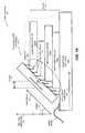
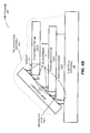
- FIG. 1A presents a block diagram illustrating a side view of chip package 100 that includes a set of chips or semiconductor dies 110 arranged in a stack 116 along a vertical direction 120, which is substantially perpendicular to a plane that is parallel to semiconductor die 110-1.
- each semiconductor die after semiconductor die 110-1 (such as semiconductor die 110-2) may be offset in a horizontal direction 118 in the plane by at least a minimum offset value 126 from an immediately preceding semiconductor die in vertical stack 116, thereby defining a stepped terrace 128 at one side of vertical stack 116 (having a constant angle 124).
- chip package 100 includes a ramp component 112, which is electrically and mechanically coupled to semiconductor dies 110. This ramp component is positioned on the one side of vertical stack 116, and is approximately parallel to a direction 122 along stepped terrace 128, which is between horizontal direction 118 and vertical direction 120.
- semiconductor dies 110 are fabricated using standard silicon processing. In particular, in these embodiments semiconductor dies 110 do not include TSVs. These semiconductor dies may provide silicon area that supports logic and/or memory functionality.
- semiconductor dies 110 may communicate with each other, and with an external device(s) or system(s), via ramp component 112.
- ramp component 112 may be electrically coupled to each of semiconductor dies 110 via microsprings 114.
- microsprings 114 can be fabricated on a wide variety of surfaces, including: a printed circuit board (PCB), an organic or ceramic integrated circuit (IC), and/or on the surface of a semiconductor die.
- microsprings 114 can be fabricated with an areal density of inter-chip connections that exceeds the density of input/output (I / O) signals on high performance ICs, and the compliance of microsprings 114 can increase the tolerance to mechanical movement and misalignment of components in chip package 100.
- Microsprings 114 can also provide mechanical and electrical contacts without the use of solder.
- the mechanical and/or the electrical coupling between ramp component 112 and semiconductor dies 110 can be removable or remateable (i.e., these components can be remateably coupled), which facilitates rework of chip package 100 during and/or after assembly and test.
- remateable mechanical or electrical coupling should be understood to be mechanical or electrical coupling that can be established and broken repeatedly ( i.e., two or more times) without requiring rework or heating (such as with solder).
- the remateable mechanical or electrical coupling involves male and female components that designed to couple to each other (such as components that snap together).
- remateable components are components that are configured to allow remateable coupling to be established.
- the mechanical and/or the electrical coupling between ramp component 112 and semiconductor dies 110 is more permanent (for example, it may not be remateable, such as solder contacts).
- ramp component 112 may be a passive component, such as a plastic substrate with metal traces to electrically couple to semiconductor dies 110.
- ramp component 112 may be fabricated using injection-molded plastic.
- ramp component 112 may be another semiconductor die with lithographically defined wires or signal lines.
- active devices such as limit amplifiers, may be included to reduced cross-talk between the signal lines. Additionally, cross-talk may be reduced in either an active or a passive ramp component 112 using differential signaling.
- ramp component 112 includes transistors and wires that shuttle data and power signals among semiconductor dies 110 via microsprings 114.
- ramp component 112 may include high-voltage signals. These signals may be stepped down for use on semiconductor dies 110 using: a step-down regulator (such as a capacitor-to-capacitor step-down regulator), as well as capacitor and/or inductor discrete components to couple to semiconductor dies 110.
- a step-down regulator such as a capacitor-to-capacitor step-down regulator
- capacitor and/or inductor discrete components to couple to semiconductor dies 110.
- chip package 100 includes an optional substrate 130 under semiconductor die 110-1, which is approximately parallel to the plane.
- This optional substrate 130 is at least electrically coupled to ramp component 112 (which may facilitate communication of electrical or power signals with semiconductor dies 110 without using TSVs in semiconductor dies 110), and may be rigidly mechanically coupled to semiconductor die 110-1.
- optional substrate 130 may include: a buffer or logic chip for memory, and/or input/output (IlO) to external device(s) and/or system(s).
- the I/O may include one or more ball-bonds or wire bonds (as illustrated in FIG. 1A ).
- FIG. 1B presents a block diagram illustrating a top view of chip package 100, with four semiconductor dies 110. This figure shows that optional substrate 130 may extend beyond stack 116 ( FIG. 1A ) so that up to four edges of optional substrate 130 may be accessible for communication, using: wire bonding, ball-bonds, and/or proximity communication (PxC).
- PxC proximity communication
- semiconductor dies 110 and ramp component 112, ramp component 112 and optional substrate 130, optional substrate 130 and external device(s) or system(s), and/or ramp component 112 and external device(s) or system(s) may communicate with each other using PxC of electromagnetically coupled signals (which is referred to as 'electromagnetic proximity communication'), such as capacitively coupled signals and/or proximity communication of optical signals (which are, respectively, referred to as 'electrical proximity communication' and 'optical proximity communication').
- the electromagnetic proximity communication includes inductively coupled signals and/or conductively coupled signals.
- transmit and receive I / O circuits may be used in components in chip package 100.
- the transmit and receive I / O circuits may include one or more embodiments described in U.S. patent application 12/425,871, entitled “Receive Circuit for Connectors with Variable Complex Impedance,” by Robert J. Drost et al. , Attorney Docket Number SUN09-0285, filed on April 17, 2009, the contents of which are hereby incorporated by reference.
- microspring 114 there may be two or more microspring 114 geometries on a given semiconductor die.
- data-signal microsprings may be short with blunt ends, while power-signal microsprings may be longer with sharper tips.
- redundant power-signal microsprings yield and long-term reliability may be enhanced even if some number of the power-signal microsprings lose their connections.
- a conductive liquid, paste or film may be added to the contact area to fill in any gaps. This would also have the beneficial effect of increasing the area of overlap to the extent that the liquid, paste or film extends beyond the edges of the given microspring.
- FIGs. 1A and 1B illustrate a particular configuration of chip package 100
- a number of techniques and configurations may be used to implement: electrical contact, mechanical alignment, assembly, and/or electrical I / O with ramp component 112 and/or optional substrate 130. We now describe several of these embodiments.
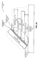
- FIG. 2A presents a block diagram illustrating a chip package 200 in which ramp component 112 is electrically coupled to semiconductor dies 110 by an anisotropic film 210, such as an anisotropic elastomer film (which is sometimes referred to as an 'anisotropic conductive film').
- anisotropic film 210 such as an anisotropic elastomer film (which is sometimes referred to as an 'anisotropic conductive film').
- anisotropic film 210 enhance electrical conductivity normal to the surface of anisotropic film 210 while also diminishing electrical conductivity tangential to the surface of anisotropic film 210.
- anisotropic film 210 electrically couples mechanically aligned pads on opposite faces of anisotropic film 210.
- the impedance of the resulting electrical contacts may be conductive and/or capacitive. If the impedance is conductive, conventional transmit and receive I / O circuits may be used in components in chip package 200. However, if the impedance is complex, the transmit and receive I / O circuits in chip package 200 may include one or more embodiments described in U.S. patent application 12/425,871 .
- electrical coupling between semiconductor dies 110 and ramp component 112 via anisotropic film 210 is facilitated using compression elements on top surfaces of semiconductor dies 110 and/or ramp component 112 (for example, compression elements 212-1 and 214-1) that compress anisotropic film 210 when chip package 200 is assembled.
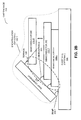
- FIG. 3A presents a block diagram illustrating a chip package 300.
- Area solder bonds 312 may be used to electrically couple optional substrate 130 to other semiconductor die(s) and/or PCB (s).
- the added cost may be more tolerable in optional substrate 130 because it is often a more expensive chip that is used once per chip package. It is also conceivable that a combination of wire bonds and TSVs could be used on the same optional substrate 130.
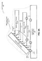
- FIG. 4A presents a block diagram illustrating a chip package 400 that includes balls (such as ball 410-1) and associated pits (such as pit 412-1).
- the ball-and-etch-pit alignment technique can align the surfaces of semiconductor dies 110 and/or optional substrate 130 with mechanical tolerances of less than a micron under slight pressure that snaps the surfaces together. Before applying this pressure, pick-and-place machines can be used to achieve mechanical tolerances of less than 10 ⁇ m when placing components together.
- these machines can align the components with mechanical tolerances of less than a micron. Given these initial alignments, it is possible to then adhere the optional substrate 130 and semiconductor dies 110 to form a spatially well-defined terrace 128 among semiconductor dies 110. In this example, it may be sufficient to align ramp component 112 to optional substrate 130 or to at least one of semiconductor dies 110.
- a minimal arrangement may use two pits to fix the x-y position of the surface of ramp component 112 to optional substrate 130 and to the group of semiconductor dies 110.
- a mechanical force applied to the backs of ramp component 112 and optional substrate 130 would then press ramp component 112 into contact with optional substrate 130 and semiconductor dies 110.
- thermal distortions and other mechanical forces may prevent a weakly adhesive technique from providing a robust long-term chip-packaging technique.
- strong, permanent-adhesion of optional substrate 130 and semiconductor dies 110 is robust, it may prevent rework during assembly and test and/or after deployment.
- packaging techniques that allow some rework are more cost-effective when faced with lower semiconductor-die yields or high expense to test extensively before packaging and assembly. Thus, there may be advantages to packaging techniques that avoid strong adhesives.
- electronic alignment techniques are used to correct for planar mechanical misalignments in a chip package.
- electronic alignment may be used with conductive and/or capacitive contacts if a given microspring contacts an array of transmit or receive micropads or microbars.
- stack 116 ( FIG. 1 A) contains DRAM memory cells and some of the support circuits for those memory cells.
- optional substrate 130 contains I / O circuits and/or additional DRAM support circuits (such as circuits to select bit, row, column, block, and/or bank, as well as chip redundancy).
- stack 116 ( FIG. 1A ) may contain static random access memory (SRAM) macros and some of the support circuits for those macros.
- optional substrate 130 may include additional SRAM support circuits (such as redundancy), as well as switch and I / O circuits.
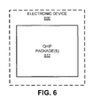
- FIG. 6 presents a block diagram illustrating an electronic device 600 that includes one or more chip packages 612, such as one of the previous embodiments of a chip package.
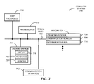
- FIG. 7 presents a block diagram illustrating a computer system 700 that includes one or more chip packages 708, such as one of the previous embodiments of a chip package.
- Computer system 700 includes: one or more processors (or processor cores) 710, a communication interface 712, a user interface 714, and one or more signal lines 722 coupling these components together.
- the one or more processors (or processor cores) 710 may support parallel processing and/or multi-threaded operation
- the communication interface 712 may have a persistent communication connection
- the one or more signal lines 722 may constitute a communication bus.
- the user interface 714 may include: a display 716, a keyboard 718, and/or a pointer 720, such as a mouse.
- Memory 724 may also include one or more program modules 730 (or a set of instructions). Note that one or more of program modules 730 may constitute a computer-program mechanism. Instructions in the various modules in the memory 724 may be implemented in: a high-level procedural language, an object-oriented programming language, and/or in an assembly or machine language. The programming language may be compiled or interpreted, i.e., configurable or configured, to be executed by the one or more processors (or processor cores) 710.
- Computer system 700 may include, but is not limited to: a server, a laptop computer, a personal computer, a work station, a mainframe computer, a blade, an enterprise computer, a data center, a portable-computing device, a supercomputer, a network-attached-storage (NAS) system, a storage-area-network (SAN ) system, and/or another electronic computing device.
- chip package(s) 708 may be included in a backplane that is coupled to multiple processor blades, or chip package(s) 708 may couple different types of components (such as processors, memory, I / O devices, and/or peripheral devices).
- chip package(s) 708 may perform the functions of: a switch, a hub, a bridge, and/or a router.
- computer system 700 may be at one location or may be distributed over multiple, geographically dispersed locations.
- Chip package 100 ( FIGs. 1A and 1B ), chip package 200 ( FIG. 2A ), chip package 250 ( FIG. 2B ), chip package 300 ( FIG. 3A ), chip package 330 ( FIG. 3B ), chip package 360 ( FIG. 3C ), chip package 380 ( FIG. 3D ), chip package 400 ( FIG. 4A ), chip package 450 ( FIG. 4B ), chip package 500 ( FIG. 5 ), electronic device 600 ( FIG. 6 ) and/or computer system 700 may include fewer components or additional components.
- semiconductor dies 110 in stack 116 may have different thicknesses or widths.
- the offsets in the horizontal positions of thicker semiconductor dies 110 may be larger than the offsets in the horizontal positions of thinner semiconductor dies 110.
- ramp component 112 may include additional supply decoupling capacitors, for example, by fabricating the capacitors on a silicon die or by soldering discrete capacitors to its back surface and using TSVs or, in another technique, to electrically connect the discrete capacitors to the power-supply delivery or regulation circuits. Power may also be delivered through an actively regulated network.
- circuits such as buck converters or capacitor-to-capacitor converters, may be included on ramp component 112 and/or optional substrate 130 to improve the quality of the power supply delivered to semiconductor dies 110.
- electronic device 600 may be implemented in one or more application-specific integrated circuits (ASICs) and/or one or more digital signal processors (DSPs).
- ASICs application-specific integrated circuits
- DSPs digital signal processors
- functionality in the preceding embodiments may be implemented more in hardware and less in software, or less in hardware and more in software, as is known in the art.
- semiconductor dies 110 such as silicon
- a different material than a semiconductor may be used as the substrate material in one or more of these chips.
Landscapes
- Semiconductor Integrated Circuits (AREA)
- Internal Circuitry In Semiconductor Integrated Circuit Devices (AREA)
Applications Claiming Priority (2)
| Application Number | Priority Date | Filing Date | Title |
|---|---|---|---|
| US12/507,349 US8476749B2 (en) | 2009-07-22 | 2009-07-22 | High-bandwidth ramp-stack chip package |
| EP10737694A EP2457253A1 (de) | 2009-07-22 | 2010-07-09 | Ramp-stack-chipgehäuse mit hoher bandbreite |
Related Parent Applications (1)
| Application Number | Title | Priority Date | Filing Date |
|---|---|---|---|
| EP10737694A Division EP2457253A1 (de) | 2009-07-22 | 2010-07-09 | Ramp-stack-chipgehäuse mit hoher bandbreite |
Publications (2)
| Publication Number | Publication Date |
|---|---|
| EP2958143A1 true EP2958143A1 (de) | 2015-12-23 |
| EP2958143B1 EP2958143B1 (de) | 2017-12-27 |
Family
ID=42617446
Family Applications (2)
| Application Number | Title | Priority Date | Filing Date |
|---|---|---|---|
| EP15177142.5A Active EP2958143B1 (de) | 2009-07-22 | 2010-07-09 | Rampen-stapel-chipgehäuse mit mechanischen rasten und mikrofedern |
| EP10737694A Ceased EP2457253A1 (de) | 2009-07-22 | 2010-07-09 | Ramp-stack-chipgehäuse mit hoher bandbreite |
Family Applications After (1)
| Application Number | Title | Priority Date | Filing Date |
|---|---|---|---|
| EP10737694A Ceased EP2457253A1 (de) | 2009-07-22 | 2010-07-09 | Ramp-stack-chipgehäuse mit hoher bandbreite |
Country Status (5)
| Country | Link |
|---|---|
| US (1) | US8476749B2 (de) |
| EP (2) | EP2958143B1 (de) |
| CN (1) | CN102484108B (de) |
| TW (1) | TWI503948B (de) |
| WO (1) | WO2011011212A1 (de) |
Families Citing this family (14)
| Publication number | Priority date | Publication date | Assignee | Title |
|---|---|---|---|---|
| US8373280B2 (en) * | 2010-09-01 | 2013-02-12 | Oracle America, Inc. | Manufacturing fixture for a ramp-stack chip package using solder for coupling a ramp component |
| US8283766B2 (en) * | 2010-09-02 | 2012-10-09 | Oracle America, Inc | Ramp-stack chip package with static bends |
| US8390109B2 (en) * | 2011-02-17 | 2013-03-05 | Oracle America, Inc. | Chip package with plank stack of semiconductor dies |
| US9082632B2 (en) * | 2012-05-10 | 2015-07-14 | Oracle International Corporation | Ramp-stack chip package with variable chip spacing |
| CN104350593B (zh) * | 2012-06-25 | 2017-12-05 | 英特尔公司 | 具有居间垂直侧边芯片的多管芯半导体结构及其半导体封装 |
| KR101880173B1 (ko) * | 2012-07-11 | 2018-07-19 | 에스케이하이닉스 주식회사 | 멀티 칩 패키지 |
| US9218157B2 (en) | 2012-09-20 | 2015-12-22 | Oracle International Corporation | Performing a division operation using a split division circuit |
| KR20140075340A (ko) * | 2012-12-11 | 2014-06-19 | 에스케이하이닉스 주식회사 | 반도체 장치 및 그 제조 방법 |
| KR20150018099A (ko) * | 2013-08-09 | 2015-02-23 | 에스케이하이닉스 주식회사 | 적층 반도체 장치 |
| US9209165B2 (en) | 2013-10-21 | 2015-12-08 | Oracle International Corporation | Technique for controlling positions of stacked dies |
| WO2017111952A1 (en) * | 2015-12-22 | 2017-06-29 | Intel Corporation | Ultra small molded module integrated with die by module-on-wafer assembly |
| JP6718749B2 (ja) * | 2016-06-06 | 2020-07-08 | ローム株式会社 | モータ制御装置 |
| US20190279962A1 (en) * | 2018-03-09 | 2019-09-12 | Oracle International Corporation | Method and apparatus for stacking warped chips to assemble three-dimensional integrated circuits |
| KR102810486B1 (ko) * | 2020-09-08 | 2025-05-21 | 에스케이하이닉스 주식회사 | 수동 소자를 포함한 스택 패키지 |
Citations (3)
| Publication number | Priority date | Publication date | Assignee | Title |
|---|---|---|---|---|
| US4778950A (en) | 1985-07-22 | 1988-10-18 | Digital Equipment Corporation | Anisotropic elastomeric interconnecting system |
| US5624268A (en) | 1993-11-10 | 1997-04-29 | The Whitaker Corporation | Electrical connectors using anisotropic conductive films |
| US20070278641A1 (en) * | 2005-06-14 | 2007-12-06 | John Trezza | Side Stacking Apparatus and Method |
Family Cites Families (39)
| Publication number | Priority date | Publication date | Assignee | Title |
|---|---|---|---|---|
| US4500905A (en) * | 1981-09-30 | 1985-02-19 | Tokyo Shibaura Denki Kabushiki Kaisha | Stacked semiconductor device with sloping sides |
| JPH088321B2 (ja) * | 1987-01-19 | 1996-01-29 | 住友電気工業株式会社 | 集積回路パツケ−ジ |
| US5422435A (en) * | 1992-05-22 | 1995-06-06 | National Semiconductor Corporation | Stacked multi-chip modules and method of manufacturing |
| US5703436A (en) * | 1994-12-13 | 1997-12-30 | The Trustees Of Princeton University | Transparent contacts for organic devices |
| US5998864A (en) * | 1995-05-26 | 1999-12-07 | Formfactor, Inc. | Stacking semiconductor devices, particularly memory chips |
| US6888362B2 (en) * | 2000-11-09 | 2005-05-03 | Formfactor, Inc. | Test head assembly for electronic components with plurality of contoured microelectronic spring contacts |
| JP3765952B2 (ja) * | 1999-10-19 | 2006-04-12 | 富士通株式会社 | 半導体装置 |
| JP3822768B2 (ja) * | 1999-12-03 | 2006-09-20 | 株式会社ルネサステクノロジ | Icカードの製造方法 |
| US6376904B1 (en) * | 1999-12-23 | 2002-04-23 | Rambus Inc. | Redistributed bond pads in stacked integrated circuit die package |
| US6621155B1 (en) * | 1999-12-23 | 2003-09-16 | Rambus Inc. | Integrated circuit device having stacked dies and impedance balanced transmission lines |
| JP3768761B2 (ja) * | 2000-01-31 | 2006-04-19 | 株式会社日立製作所 | 半導体装置およびその製造方法 |
| NO20001360D0 (no) * | 2000-03-15 | 2000-03-15 | Thin Film Electronics Asa | Vertikale elektriske forbindelser i stabel |
| WO2001080315A2 (en) * | 2000-04-12 | 2001-10-25 | Formfactor, Inc. | Shaped springs and methods of fabricating and using shaped springs |
| US6418033B1 (en) * | 2000-11-16 | 2002-07-09 | Unitive Electronics, Inc. | Microelectronic packages in which second microelectronic substrates are oriented relative to first microelectronic substrates at acute angles |
| US6900528B2 (en) * | 2001-06-21 | 2005-05-31 | Micron Technology, Inc. | Stacked mass storage flash memory package |
| JP2004063579A (ja) * | 2002-07-25 | 2004-02-26 | Renesas Technology Corp | 積層型半導体装置 |
| JP2004071947A (ja) * | 2002-08-08 | 2004-03-04 | Renesas Technology Corp | 半導体装置 |
| JP3867785B2 (ja) | 2002-10-15 | 2007-01-10 | セイコーエプソン株式会社 | 光モジュール |
| AU2003301632A1 (en) * | 2002-10-22 | 2004-05-13 | Unitive International Limited | Stacked electronic structures including offset substrates |
| KR100499289B1 (ko) * | 2003-02-07 | 2005-07-04 | 삼성전자주식회사 | 패턴 리드를 갖는 반도체 패키지 및 그 제조 방법 |
| JP2007066922A (ja) * | 2003-11-28 | 2007-03-15 | Renesas Technology Corp | 半導体集積回路装置 |
| US7015586B2 (en) * | 2004-07-08 | 2006-03-21 | Kingpak Technology Inc. | Stacked structure of integrated circuits |
| US7582963B2 (en) * | 2005-03-29 | 2009-09-01 | Texas Instruments Incorporated | Vertically integrated system-in-a-package |
| US20060290377A1 (en) * | 2005-05-31 | 2006-12-28 | Jongsun Kim | Capacitively coupled pulsed signaling bus interface |
| US7573720B1 (en) * | 2005-06-15 | 2009-08-11 | Sun Microsystems, Inc. | Active socket for facilitating proximity communication |
| JP2007134486A (ja) * | 2005-11-10 | 2007-05-31 | Toshiba Corp | 積層型半導体装置及びその製造方法 |
| TWI284971B (en) * | 2006-01-26 | 2007-08-01 | Siliconware Precision Industries Co Ltd | Multichip stack structure |
| US7977579B2 (en) * | 2006-03-30 | 2011-07-12 | Stats Chippac Ltd. | Multiple flip-chip integrated circuit package system |
| US7420269B2 (en) * | 2006-04-18 | 2008-09-02 | Stats Chippac Ltd. | Stacked integrated circuit package-in-package system |
| TWI306658B (en) * | 2006-08-07 | 2009-02-21 | Chipmos Technologies Inc | Leadframe on offset stacked chips package |
| US7592691B2 (en) * | 2006-09-01 | 2009-09-22 | Micron Technology, Inc. | High density stacked die assemblies, structures incorporated therein and methods of fabricating the assemblies |
| TW200814249A (en) * | 2006-09-12 | 2008-03-16 | Chipmos Technologies Inc | Stacked chip package structure with lead-frame having bus bar |
| TWI358815B (en) * | 2006-09-12 | 2012-02-21 | Chipmos Technologies Inc | Stacked chip package structure with lead-frame hav |
| TWI378539B (en) * | 2006-10-26 | 2012-12-01 | Chipmos Technologies Inc | Stacked chip package structure with lead-frame having inner leads with transfer pad |
| TW200820402A (en) * | 2006-10-26 | 2008-05-01 | Chipmos Technologies Inc | Stacked chip packaging with heat sink struct |
| TWI357640B (en) * | 2007-01-24 | 2012-02-01 | Siliconware Precision Industries Co Ltd | Multichip stacking structure and fabricating metho |
| US7911045B2 (en) * | 2007-08-17 | 2011-03-22 | Kabushiki Kaisha Toshiba | Semiconductor element and semiconductor device |
| US7952183B2 (en) * | 2007-10-29 | 2011-05-31 | Kabushiki Kaisha Toshiba | High capacity memory with stacked layers |
| JP4776675B2 (ja) * | 2008-10-31 | 2011-09-21 | 株式会社東芝 | 半導体メモリカード |
-
2009
- 2009-07-22 US US12/507,349 patent/US8476749B2/en active Active
-
2010
- 2010-07-08 TW TW099122481A patent/TWI503948B/zh active
- 2010-07-09 CN CN201080032861.8A patent/CN102484108B/zh active Active
- 2010-07-09 EP EP15177142.5A patent/EP2958143B1/de active Active
- 2010-07-09 WO PCT/US2010/041524 patent/WO2011011212A1/en not_active Ceased
- 2010-07-09 EP EP10737694A patent/EP2457253A1/de not_active Ceased
Patent Citations (3)
| Publication number | Priority date | Publication date | Assignee | Title |
|---|---|---|---|---|
| US4778950A (en) | 1985-07-22 | 1988-10-18 | Digital Equipment Corporation | Anisotropic elastomeric interconnecting system |
| US5624268A (en) | 1993-11-10 | 1997-04-29 | The Whitaker Corporation | Electrical connectors using anisotropic conductive films |
| US20070278641A1 (en) * | 2005-06-14 | 2007-12-06 | John Trezza | Side Stacking Apparatus and Method |
Also Published As
| Publication number | Publication date |
|---|---|
| EP2457253A1 (de) | 2012-05-30 |
| CN102484108A (zh) | 2012-05-30 |
| TWI503948B (zh) | 2015-10-11 |
| US8476749B2 (en) | 2013-07-02 |
| US20110018120A1 (en) | 2011-01-27 |
| WO2011011212A1 (en) | 2011-01-27 |
| TW201123406A (en) | 2011-07-01 |
| EP2958143B1 (de) | 2017-12-27 |
| CN102484108B (zh) | 2014-12-17 |
Similar Documents
| Publication | Publication Date | Title |
|---|---|---|
| EP2958143B1 (de) | Rampen-stapel-chipgehäuse mit mechanischen rasten und mikrofedern | |
| EP2847793B1 (de) | Gehäuse mit stufenförmigem chipstapel und rampen-verbindungsbauteil | |
| US8283766B2 (en) | Ramp-stack chip package with static bends | |
| EP2612355B1 (de) | Ramp-stack-chipgehäuse und seine herstellungsmethode | |
| US8772920B2 (en) | Interconnection and assembly of three-dimensional chip packages | |
| US9209165B2 (en) | Technique for controlling positions of stacked dies | |
| US8975754B2 (en) | Chip package for high-count chip stacks | |
| US20140225284A1 (en) | Low-cost chip package for chip stacks |
Legal Events
| Date | Code | Title | Description |
|---|---|---|---|
| PUAI | Public reference made under article 153(3) epc to a published international application that has entered the european phase |
Free format text: ORIGINAL CODE: 0009012 |
|
| AC | Divisional application: reference to earlier application |
Ref document number: 2457253 Country of ref document: EP Kind code of ref document: P |
|
| AK | Designated contracting states |
Kind code of ref document: A1 Designated state(s): AL AT BE BG CH CY CZ DE DK EE ES FI FR GB GR HR HU IE IS IT LI LT LU LV MC MK MT NL NO PL PT RO SE SI SK SM TR |
|
| 17P | Request for examination filed |
Effective date: 20160617 |
|
| RBV | Designated contracting states (corrected) |
Designated state(s): AL AT BE BG CH CY CZ DE DK EE ES FI FR GB GR HR HU IE IS IT LI LT LU LV MC MK MT NL NO PL PT RO SE SI SK SM TR |
|
| 17Q | First examination report despatched |
Effective date: 20160712 |
|
| STAA | Information on the status of an ep patent application or granted ep patent |
Free format text: STATUS: EXAMINATION IS IN PROGRESS |
|
| GRAP | Despatch of communication of intention to grant a patent |
Free format text: ORIGINAL CODE: EPIDOSNIGR1 |
|
| STAA | Information on the status of an ep patent application or granted ep patent |
Free format text: STATUS: GRANT OF PATENT IS INTENDED |
|
| RIC1 | Information provided on ipc code assigned before grant |
Ipc: H01L 21/60 20060101ALI20170623BHEP Ipc: H01L 25/065 20060101AFI20170623BHEP Ipc: H01L 23/28 20060101ALN20170623BHEP |
|
| RIC1 | Information provided on ipc code assigned before grant |
Ipc: H01L 23/28 20060101ALN20170704BHEP Ipc: H01L 21/60 20060101ALI20170704BHEP Ipc: H01L 25/065 20060101AFI20170704BHEP |
|
| INTG | Intention to grant announced |
Effective date: 20170719 |
|
| GRAA | (expected) grant |
Free format text: ORIGINAL CODE: 0009210 |
|
| GRAS | Grant fee paid |
Free format text: ORIGINAL CODE: EPIDOSNIGR3 |
|
| STAA | Information on the status of an ep patent application or granted ep patent |
Free format text: STATUS: THE PATENT HAS BEEN GRANTED |
|
| AC | Divisional application: reference to earlier application |
Ref document number: 2457253 Country of ref document: EP Kind code of ref document: P |
|
| AK | Designated contracting states |
Kind code of ref document: B1 Designated state(s): AL AT BE BG CH CY CZ DE DK EE ES FI FR GB GR HR HU IE IS IT LI LT LU LV MC MK MT NL NO PL PT RO SE SI SK SM TR |
|
| REG | Reference to a national code |
Ref country code: GB Ref legal event code: FG4D |
|
| REG | Reference to a national code |
Ref country code: CH Ref legal event code: EP |
|
| REG | Reference to a national code |
Ref country code: AT Ref legal event code: REF Ref document number: 958990 Country of ref document: AT Kind code of ref document: T Effective date: 20180115 |
|
| REG | Reference to a national code |
Ref country code: IE Ref legal event code: FG4D |
|
| REG | Reference to a national code |
Ref country code: DE Ref legal event code: R096 Ref document number: 602010047728 Country of ref document: DE |
|
| PG25 | Lapsed in a contracting state [announced via postgrant information from national office to epo] |
Ref country code: LT Free format text: LAPSE BECAUSE OF FAILURE TO SUBMIT A TRANSLATION OF THE DESCRIPTION OR TO PAY THE FEE WITHIN THE PRESCRIBED TIME-LIMIT Effective date: 20171227 Ref country code: NO Free format text: LAPSE BECAUSE OF FAILURE TO SUBMIT A TRANSLATION OF THE DESCRIPTION OR TO PAY THE FEE WITHIN THE PRESCRIBED TIME-LIMIT Effective date: 20180327 Ref country code: FI Free format text: LAPSE BECAUSE OF FAILURE TO SUBMIT A TRANSLATION OF THE DESCRIPTION OR TO PAY THE FEE WITHIN THE PRESCRIBED TIME-LIMIT Effective date: 20171227 |
|
| REG | Reference to a national code |
Ref country code: NL Ref legal event code: MP Effective date: 20171227 |
|
| REG | Reference to a national code |
Ref country code: LT Ref legal event code: MG4D |
|
| REG | Reference to a national code |
Ref country code: AT Ref legal event code: MK05 Ref document number: 958990 Country of ref document: AT Kind code of ref document: T Effective date: 20171227 |
|
| PG25 | Lapsed in a contracting state [announced via postgrant information from national office to epo] |
Ref country code: BG Free format text: LAPSE BECAUSE OF FAILURE TO SUBMIT A TRANSLATION OF THE DESCRIPTION OR TO PAY THE FEE WITHIN THE PRESCRIBED TIME-LIMIT Effective date: 20180327 Ref country code: GR Free format text: LAPSE BECAUSE OF FAILURE TO SUBMIT A TRANSLATION OF THE DESCRIPTION OR TO PAY THE FEE WITHIN THE PRESCRIBED TIME-LIMIT Effective date: 20180328 Ref country code: HR Free format text: LAPSE BECAUSE OF FAILURE TO SUBMIT A TRANSLATION OF THE DESCRIPTION OR TO PAY THE FEE WITHIN THE PRESCRIBED TIME-LIMIT Effective date: 20171227 Ref country code: LV Free format text: LAPSE BECAUSE OF FAILURE TO SUBMIT A TRANSLATION OF THE DESCRIPTION OR TO PAY THE FEE WITHIN THE PRESCRIBED TIME-LIMIT Effective date: 20171227 |
|
| PG25 | Lapsed in a contracting state [announced via postgrant information from national office to epo] |
Ref country code: NL Free format text: LAPSE BECAUSE OF FAILURE TO SUBMIT A TRANSLATION OF THE DESCRIPTION OR TO PAY THE FEE WITHIN THE PRESCRIBED TIME-LIMIT Effective date: 20171227 |
|
| PG25 | Lapsed in a contracting state [announced via postgrant information from national office to epo] |
Ref country code: CY Free format text: LAPSE BECAUSE OF FAILURE TO SUBMIT A TRANSLATION OF THE DESCRIPTION OR TO PAY THE FEE WITHIN THE PRESCRIBED TIME-LIMIT Effective date: 20171227 Ref country code: EE Free format text: LAPSE BECAUSE OF FAILURE TO SUBMIT A TRANSLATION OF THE DESCRIPTION OR TO PAY THE FEE WITHIN THE PRESCRIBED TIME-LIMIT Effective date: 20171227 Ref country code: SK Free format text: LAPSE BECAUSE OF FAILURE TO SUBMIT A TRANSLATION OF THE DESCRIPTION OR TO PAY THE FEE WITHIN THE PRESCRIBED TIME-LIMIT Effective date: 20171227 Ref country code: CZ Free format text: LAPSE BECAUSE OF FAILURE TO SUBMIT A TRANSLATION OF THE DESCRIPTION OR TO PAY THE FEE WITHIN THE PRESCRIBED TIME-LIMIT Effective date: 20171227 Ref country code: ES Free format text: LAPSE BECAUSE OF FAILURE TO SUBMIT A TRANSLATION OF THE DESCRIPTION OR TO PAY THE FEE WITHIN THE PRESCRIBED TIME-LIMIT Effective date: 20171227 |
|
| PG25 | Lapsed in a contracting state [announced via postgrant information from national office to epo] |
Ref country code: AT Free format text: LAPSE BECAUSE OF FAILURE TO SUBMIT A TRANSLATION OF THE DESCRIPTION OR TO PAY THE FEE WITHIN THE PRESCRIBED TIME-LIMIT Effective date: 20171227 Ref country code: IT Free format text: LAPSE BECAUSE OF FAILURE TO SUBMIT A TRANSLATION OF THE DESCRIPTION OR TO PAY THE FEE WITHIN THE PRESCRIBED TIME-LIMIT Effective date: 20171227 Ref country code: SM Free format text: LAPSE BECAUSE OF FAILURE TO SUBMIT A TRANSLATION OF THE DESCRIPTION OR TO PAY THE FEE WITHIN THE PRESCRIBED TIME-LIMIT Effective date: 20171227 Ref country code: RO Free format text: LAPSE BECAUSE OF FAILURE TO SUBMIT A TRANSLATION OF THE DESCRIPTION OR TO PAY THE FEE WITHIN THE PRESCRIBED TIME-LIMIT Effective date: 20171227 Ref country code: IS Free format text: LAPSE BECAUSE OF FAILURE TO SUBMIT A TRANSLATION OF THE DESCRIPTION OR TO PAY THE FEE WITHIN THE PRESCRIBED TIME-LIMIT Effective date: 20180427 Ref country code: PL Free format text: LAPSE BECAUSE OF FAILURE TO SUBMIT A TRANSLATION OF THE DESCRIPTION OR TO PAY THE FEE WITHIN THE PRESCRIBED TIME-LIMIT Effective date: 20171227 |
|
| REG | Reference to a national code |
Ref country code: DE Ref legal event code: R097 Ref document number: 602010047728 Country of ref document: DE |
|
| PLBE | No opposition filed within time limit |
Free format text: ORIGINAL CODE: 0009261 |
|
| STAA | Information on the status of an ep patent application or granted ep patent |
Free format text: STATUS: NO OPPOSITION FILED WITHIN TIME LIMIT |
|
| PG25 | Lapsed in a contracting state [announced via postgrant information from national office to epo] |
Ref country code: DK Free format text: LAPSE BECAUSE OF FAILURE TO SUBMIT A TRANSLATION OF THE DESCRIPTION OR TO PAY THE FEE WITHIN THE PRESCRIBED TIME-LIMIT Effective date: 20171227 |
|
| 26N | No opposition filed |
Effective date: 20180928 |
|
| PG25 | Lapsed in a contracting state [announced via postgrant information from national office to epo] |
Ref country code: SI Free format text: LAPSE BECAUSE OF FAILURE TO SUBMIT A TRANSLATION OF THE DESCRIPTION OR TO PAY THE FEE WITHIN THE PRESCRIBED TIME-LIMIT Effective date: 20171227 |
|
| REG | Reference to a national code |
Ref country code: CH Ref legal event code: PL |
|
| PG25 | Lapsed in a contracting state [announced via postgrant information from national office to epo] |
Ref country code: MC Free format text: LAPSE BECAUSE OF FAILURE TO SUBMIT A TRANSLATION OF THE DESCRIPTION OR TO PAY THE FEE WITHIN THE PRESCRIBED TIME-LIMIT Effective date: 20171227 Ref country code: LU Free format text: LAPSE BECAUSE OF NON-PAYMENT OF DUE FEES Effective date: 20180709 |
|
| REG | Reference to a national code |
Ref country code: BE Ref legal event code: MM Effective date: 20180731 |
|
| REG | Reference to a national code |
Ref country code: IE Ref legal event code: MM4A |
|
| PG25 | Lapsed in a contracting state [announced via postgrant information from national office to epo] |
Ref country code: IE Free format text: LAPSE BECAUSE OF NON-PAYMENT OF DUE FEES Effective date: 20180709 Ref country code: LI Free format text: LAPSE BECAUSE OF NON-PAYMENT OF DUE FEES Effective date: 20180731 Ref country code: CH Free format text: LAPSE BECAUSE OF NON-PAYMENT OF DUE FEES Effective date: 20180731 Ref country code: FR Free format text: LAPSE BECAUSE OF NON-PAYMENT OF DUE FEES Effective date: 20180731 |
|
| PG25 | Lapsed in a contracting state [announced via postgrant information from national office to epo] |
Ref country code: BE Free format text: LAPSE BECAUSE OF NON-PAYMENT OF DUE FEES Effective date: 20180731 |
|
| PG25 | Lapsed in a contracting state [announced via postgrant information from national office to epo] |
Ref country code: MT Free format text: LAPSE BECAUSE OF NON-PAYMENT OF DUE FEES Effective date: 20180709 |
|
| PG25 | Lapsed in a contracting state [announced via postgrant information from national office to epo] |
Ref country code: TR Free format text: LAPSE BECAUSE OF FAILURE TO SUBMIT A TRANSLATION OF THE DESCRIPTION OR TO PAY THE FEE WITHIN THE PRESCRIBED TIME-LIMIT Effective date: 20171227 |
|
| PG25 | Lapsed in a contracting state [announced via postgrant information from national office to epo] |
Ref country code: PT Free format text: LAPSE BECAUSE OF FAILURE TO SUBMIT A TRANSLATION OF THE DESCRIPTION OR TO PAY THE FEE WITHIN THE PRESCRIBED TIME-LIMIT Effective date: 20171227 |
|
| PG25 | Lapsed in a contracting state [announced via postgrant information from national office to epo] |
Ref country code: SE Free format text: LAPSE BECAUSE OF FAILURE TO SUBMIT A TRANSLATION OF THE DESCRIPTION OR TO PAY THE FEE WITHIN THE PRESCRIBED TIME-LIMIT Effective date: 20171227 Ref country code: MK Free format text: LAPSE BECAUSE OF NON-PAYMENT OF DUE FEES Effective date: 20171227 Ref country code: HU Free format text: LAPSE BECAUSE OF FAILURE TO SUBMIT A TRANSLATION OF THE DESCRIPTION OR TO PAY THE FEE WITHIN THE PRESCRIBED TIME-LIMIT; INVALID AB INITIO Effective date: 20100709 |
|
| PG25 | Lapsed in a contracting state [announced via postgrant information from national office to epo] |
Ref country code: AL Free format text: LAPSE BECAUSE OF FAILURE TO SUBMIT A TRANSLATION OF THE DESCRIPTION OR TO PAY THE FEE WITHIN THE PRESCRIBED TIME-LIMIT Effective date: 20171227 |
|
| P01 | Opt-out of the competence of the unified patent court (upc) registered |
Effective date: 20230523 |
|
| REG | Reference to a national code |
Ref country code: DE Ref legal event code: R079 Ref document number: 602010047728 Country of ref document: DE Free format text: PREVIOUS MAIN CLASS: H01L0025065000 Ipc: H10D0080300000 |
|
| PGFP | Annual fee paid to national office [announced via postgrant information from national office to epo] |
Ref country code: GB Payment date: 20250529 Year of fee payment: 16 |
|
| PGFP | Annual fee paid to national office [announced via postgrant information from national office to epo] |
Ref country code: DE Payment date: 20250604 Year of fee payment: 16 |