EP2958236B1 - Systeme und verfahren zur implementierung von fehlerformender, aliasfreier, asynchron umschaltender analog-digital-wandlung - Google Patents
Systeme und verfahren zur implementierung von fehlerformender, aliasfreier, asynchron umschaltender analog-digital-wandlung Download PDFInfo
- Publication number
- EP2958236B1 EP2958236B1 EP15305905.0A EP15305905A EP2958236B1 EP 2958236 B1 EP2958236 B1 EP 2958236B1 EP 15305905 A EP15305905 A EP 15305905A EP 2958236 B1 EP2958236 B1 EP 2958236B1
- Authority
- EP
- European Patent Office
- Prior art keywords
- signal
- output
- comparator
- integrator
- switch
- Prior art date
- Legal status (The legal status is an assumption and is not a legal conclusion. Google has not performed a legal analysis and makes no representation as to the accuracy of the status listed.)
- Active
Links
Images






Classifications
-
- H—ELECTRICITY
- H03—ELECTRONIC CIRCUITRY
- H03M—CODING; DECODING; CODE CONVERSION IN GENERAL
- H03M1/00—Analogue/digital conversion; Digital/analogue conversion
- H03M1/12—Analogue/digital converters
-
- H—ELECTRICITY
- H03—ELECTRONIC CIRCUITRY
- H03K—PULSE TECHNIQUE
- H03K5/00—Manipulating of pulses not covered by one of the other main groups of this subclass
- H03K5/22—Circuits having more than one input and one output for comparing pulses or pulse trains with each other according to input signal characteristics, e.g. slope, integral
- H03K5/24—Circuits having more than one input and one output for comparing pulses or pulse trains with each other according to input signal characteristics, e.g. slope, integral the characteristic being amplitude
-
- H—ELECTRICITY
- H03—ELECTRONIC CIRCUITRY
- H03K—PULSE TECHNIQUE
- H03K5/00—Manipulating of pulses not covered by one of the other main groups of this subclass
- H03K5/153—Arrangements in which a pulse is delivered at the instant when a predetermined characteristic of an input signal is present or at a fixed time interval after this instant
- H03K5/1534—Transition or edge detectors
-
- H—ELECTRICITY
- H03—ELECTRONIC CIRCUITRY
- H03M—CODING; DECODING; CODE CONVERSION IN GENERAL
- H03M1/00—Analogue/digital conversion; Digital/analogue conversion
- H03M1/12—Analogue/digital converters
- H03M1/124—Sampling or signal conditioning arrangements specially adapted for A/D converters
- H03M1/1245—Details of sampling arrangements or methods
- H03M1/125—Asynchronous, i.e. free-running operation within each conversion cycle
-
- H—ELECTRICITY
- H03—ELECTRONIC CIRCUITRY
- H03M—CODING; DECODING; CODE CONVERSION IN GENERAL
- H03M1/00—Analogue/digital conversion; Digital/analogue conversion
- H03M1/12—Analogue/digital converters
- H03M1/124—Sampling or signal conditioning arrangements specially adapted for A/D converters
- H03M1/1245—Details of sampling arrangements or methods
- H03M1/1265—Non-uniform sampling
-
- H—ELECTRICITY
- H03—ELECTRONIC CIRCUITRY
- H03M—CODING; DECODING; CODE CONVERSION IN GENERAL
- H03M1/00—Analogue/digital conversion; Digital/analogue conversion
- H03M1/12—Analogue/digital converters
- H03M1/60—Analogue/digital converters with intermediate conversion to frequency of pulses
Definitions
- This disclosure relates to systems and methods for performing analog-to-digital conversion, and particularly systems and methods for performing error-shaping alias-free asynchronous analog-to-digital conversion.
- Ultra-low-power radio receivers have very tight power budgets, for example, 100 ⁇ W in wake-up receivers.
- the tight power budget in those receivers limits multichannel capabilities and blocker robustness.
- Digitization and digital signal processing (DSP) present an interesting solution, and can further enable interferer-resilient spread spectrum techniques.
- DSP digital signal processing
- ADC analog-to-digital converter
- IF intermediate frequency
- BW bandwidth
- SNDR Signal to Noise-plus-Distortion Ratio
- a Nyquist ADC cannot satisfy such a power constraint, because of its strict antialiasing filter specifications. Oversampling can simplify this requirement; however, a high sampling rate can result in a substantial power overhead, not just for the ADC, but also for subsequent processing blocks.
- US 2012/169397 A1 discloses a related asynchronous delta-sigma modulator.
- an apparatus for asynchronous analog-to-digital conversion can include an integrator circuit comprising two integrator inputs and two integrator outputs and a first switch circuit configured to couple a first apparatus input signal and a second apparatus input signal with a first integrator input and a second integrator input.
- the apparatus can also include a first comparator configured to receive a first output of the integrator circuit and a first reference signal and generate a first comparator output signal, and a second comparator configured to receive a second output of the integrator circuit and the first reference signal and generate a second comparator output signal.
- the apparatus can also include a second switch circuit configured to couple a first apparatus output and a second apparatus output with the first comparator output signal and the second comparator output signal.
- the apparatus can also include a third comparator configured to receive the first output of the integrator circuit and a second reference signal and generate a third comparator output signal, and a fourth comparator configured to receive the second output of the integrator circuit and the second reference signal, and generate a fourth comparator output signal.
- a third comparator configured to receive the first output of the integrator circuit and a second reference signal and generate a third comparator output signal
- a fourth comparator configured to receive the second output of the integrator circuit and the second reference signal, and generate a fourth comparator output signal.
- a method for asynchronous analog-to-digital conversion can include providing an integrator circuit comprising two integrator inputs and two integrator outputs, and coupling, by a first switch circuit, a first apparatus input signal and a second apparatus input signal with a first integrator input and a second integrator input.
- the method can also include receiving, by a first comparator, a first output of the integrator circuit and a first reference signal, generating, by the first comparator, a first comparator output signal, receiving, by a second comparator, a second output of the integrator circuit and the first reference signal, generating, by the second comparator, a second comparator output signal, and coupling, by a second switch circuit, a first apparatus output and a second apparatus output with the first comparator output signal and the second comparator output signal.
- the method can also include receiving, by a third comparator, the first output of the integrator circuit and a second reference signal, generating, by the third comparator, a third comparator output signal, receiving, by a fourth comparator, the second output of the integrator circuit and the second reference signal, and generating, by the fourth comparator, a fourth comparator output signal.
- An approach for power-efficient ADCs can be an asynchronous ADC, which operates in continuous time (CT) and causes no aliasing, thus requiring no antialiasing filter.
- CT continuous time
- the timing between pulses in an asynchronous digital output is an integral part of the signal representation. Accordingly, such a signal is "CT,” and can have a non-uniform signal-dependent rate that can be low enough to not overwhelm the power dissipation of the following blocks.
- the output need not be sampled in time and can be processed directly via an asynchronous CT digital approach, in which timing details, as they evolve in CT, are preserved.
- a clock-less CT DSP doing this has already been demonstrated to be power efficient.
- Fig. 1 shows the architecture of an exemplary asynchronous sigma-delta modulator (ASDM) 100.
- a first-order ASDM can include an integrator 110 and a quantizer 120.
- the quantizer 120 shown in Fig. 1 , can be a zero comparator with some hysteresis.
- ASDM 100 also has a feedback path 130, forming a feedback loop.
- ASDM 100 can encode the input signal, u(t), in the duty cycle of a binary signal, y(t). Even for a zero input, ASDM 100 can produce a 50%-duty-cycle oscillatory output. In power-constrained systems this can be an important disadvantage, as the modulator can waste energy even if there is no signal at its input.
- a proposed asynchronous CT ADC can overcome these issues, for example, by simplifying the feedback path.
- the proposed ADC can be highly power-efficient and compact, alias-free with quantization-error spectral shaping, programmable and event-driven with low output data rate, and being clock-less, can have low electromagnetic interference (EMI) emissions.
- EMI electromagnetic interference
- the present disclosure provides a system and a method wherein a delta modulator encodes the integral of the input signal u(t).
- the proposed system is different from prior-art ASDMs, for example, because the output can be, in principle, a set of impulses that can indicate the time instants where the integral of the input signal crosses the quantization levels of a given quantizer.
- the output rate of impulses can be proportional to the instantaneous value of the input signal.
- no level is crossed after the integration stage, and hence, no output is produced.
- the proposed system is asynchronous, clock-less and does not sample the input in time. Therefore, no aliasing occurs and the output has no quantization noise. For a periodic input, this can result in an output that consists of only harmonics in its spectrum. Thus, without quantization noise, the quantization harmonics can get shaped following a transfer function defined by the filter in the forward path.
- the modulation/encoding can be implemented by replacing the N-bit feedback digital-to-analog converter (DAC) in a delta modulator with a single-bit DAC.
- DAC digital-to-analog converter
- the proposed system is particularly compact and can use minimal hardware for implementation. Accordingly, it can use smaller silicon area, and hence, be cost-efficient.
- a system 200 for providing asynchronous flipping analog-to-digital conversion can comprise a first integrator 202 and a second integrator 204, a first switch 206 coupling the first integrator 202 with a first signal V INP , a second switch 208 coupling the second integrator 204 with the first signal V INP , a third switch 210 coupling the first integrator 202 with a second signal V INM , and a fourth 212 switch coupling the second integrator 204 with the second signal V INM .
- the system 200 can also comprise a first comparator 214 receiving a first threshold signal V TH and an output signal V INP_COMP of the first integrator and generating an output signal INC, a second comparator 216 receiving the first threshold signal V TH and an output signal V INM_COMP of the second integrator 204 and generating an output signal DEC.
- the system 200 can also include a logic block 218 that can receive the output signals INC and DEC of the comparators 214 and 216, can generate the control signals for switches 206, 208, 210, and 212, and can generate signals "INC_corrected” and "DEC_corrected,” which are the corrected output signals of the asynchronous flipping ADC.
- Fig. 2b illustrates an exemplary implementation of the logic block 218.
- Logic block 218 can include an OR gate 252 configured to receive the INC and DEC output signals of comparators 214 and 216.
- a flip-flop for example, a positive-edge-triggered T flip-flop 254 can receive the output of the OR gate 252 and can generate as outputs the control signals, ⁇ and ⁇ that can control switches 206, 208, 210, and 212.
- Logic block 218 can also include delay elements 256 configured to delay the outputs, ⁇ and ⁇ , of flip-flop 254 to generate delayed versions ⁇ D and ⁇ D .
- Logic block 218 can also include switches 258 that can be controlled by ⁇ D and ⁇ D , to generate, from signals INC and DEC, the outputs of the "INC_corrected” and “DEC_corrected” of the asynchronous flipping ADC of Fig. 2(a) .
- Fig. 3 shows exemplary waveforms 300 that illustrate the operation of the asynchronous flipping ADC of Fig. 2a .
- initially signal ⁇ is "1" and signal ⁇ is "0.”
- Signals V INP and V INM are both equal to zero.
- V INP and V INM are the inputs to the two integrators (202, 204) and are zero. Accordingly, the outputs of the integrators, V INP_COMP and V INM_COMP , would also remain “0.”
- the proposed architecture produces no output when the input is "0.”
- V INP_COMP After five seconds (time 302), the values of V INP and V INM can start increasing with positive and negative slopes, respectively.
- the integrators (202, 204) can start integrating these signals and produce outputs V INP_COMP and V INM_COMP as shown in Fig. 3 .
- the output, INC, of comparator 214 becomes "1" (304). This can trigger the positive-edge-triggered T flip-flop 254 in logic block 218 that can toggle the control signals ⁇ and ⁇ as show with solid and dotted lines, respectively. Following this, the inputs to the integrators are flipped and they can start integrating in the opposite direction.
- the output, INC, of comparator 214 becomes "0," which results in a narrow pulse at the comparator output. This pulse (305) can indicate the time instant at which the integrated signal crossed the first quantization level.
- the logic block contains a set of "chopping" switches 258, as illustrated in Fig. 2b , which can be similar to the ones at the inputs of the integrators, shown in Fig. 2a .
- switches 258 can be controlled by delayed versions of ⁇ and ⁇ . The delay ensures the right value is passed to the corrected outputs. The delay can be implemented using a cascade of few inverters.
- the corrected signals, "INC_corrected” and "DEC_corrected” (308), are also shown in Fig. 3 .
- the asynchronous flipping ADC thus encodes analog information in the timing of these continuous-time binary pulses. It can generate a delta-modulated output of the integral of the input signal. This is achieved with a very simple feedback structure with switches implementing the DAC.
- the output rate of impulses is proportional to the instantaneous value of the slope of the input signal.
- reconstruction is achieved by integration.
- the output rate of impulses is proportional to the instantaneous value of the input signal itself. This is illustrated in Fig. 3 .
- the integrators integrate faster and the density of the output pulses increases.
- the output activity rate is proportional to the input signal value. Reconstruction of the input signal value can thus be achieved using a low-pass filter.
- the proposed architecture uses a flipping technique to completely remove the need for charge addition and/or subtraction circuitry.
- the final structure can be extremely minimal, and hence, very area- and power-efficient.
- the generated narrow pulses can be processed digitally and in continuous time.
- the asynchronous flipping ADC When the input of the asynchronous flipping ADC has a constant value, it generates no output impulses. As the value of the input increases, the rate of impulses keeps increasing. Thus, the output activity rate is proportional to the input signal value. In an ASDM on the other hand, with a zero input, the output has a highly oscillatory nature and the frequency of oscillation drops as the input amplitude increases and approaches the full-scale value.
- the proposed asynchronous flipping ADC contains no feedback DAC, and achieves the desired functionality through additional switches which occupy less area. Besides, it can completely eliminate the power dissipation of the feedback DAC.
- the forward path contains an integrator; however, it does not necessarily increase the power consumption of the entire system as it can be a part of a preceding circuit.
- the ADC is preceded by a number of IF gain stages that amplify the signal.
- the integrator could replace one of these IF gain stages and provide some amplification. Accordingly, the added integrator can result in no or minimal increase of the power dissipation of the entire system.
- the integrator block can implement the variable gain functionality of the IF stages. This can be accomplished by putting a number of Gm stages in parallel and selectively turning ON/OFF a given number of Gm stages to vary the gain as needed.
- the output nonlinearities of the Gm stages can be quite relaxed because of the reduced signal swing at the output ([V LSB /2 V LSB /2]). The nonlinearities are then dominated solely by those associated with the input.
- the loop delay is significantly reduced.
- settling time of the DAC output occupies some of the timing budget of the loop delay.
- the loop delay is primarily dependent on the comparator delay. The other blocks contribute a negligible amount to it.
- the proposed architecture can enable a higher frequency of operation. For example, for a given resolution, it can handle a much higher frequency at its input without having any slope overload. Alternatively, for a given maximum input frequency, it can implement a much higher amplitude resolution without being limited by slope overload.
- the resolution of the modulator can be controlled by a single reference voltage, V TH , which can be set to V LSB /2. By changing its value, the resolution can be changed easily, which enables a tunable resolution.
- the proposed architecture is clock-less and can save power and area in clock generation and distribution. Similar to other continuous-time ADCs, it has no aliasing in the spectrum and a higher SNDR than Nyquist-sampling ADCs for a given amplitude resolution.
- Fig. 4 shows an exemplary architecture of a proposed asynchronous flipping ADC 400.
- the asynchronous flipping ADC 400 can be a stage between a front end circuit 450 and a reconfigurable clock-less CT digital signal processor (DSP) 460.
- DSP reconfigurable clock-less CT digital signal processor
- the proposed asynchronous flipping ADC of Fig. 4 includes two additional comparators (402, 404).
- Integrators 202 and 204 of Fig. 2a are replaced with the Gm-C integrator stage, which can include an input, INT_RST 408, for resetting the integrator outputs.
- Comparators 402 and 404 can be used to detect when the Gm stage outputs cross a reference value, for example, a value of V SAT .
- the outputs of comparators 402 and 404 can be "ORed" (412) and the output, INT_RST, can be used to reset the Gm-C integrators to the common-mode voltage.
- Fig. 5 illustrates an exemplary waveform corresponding to the proposed asynchronous flipping ADC.
- the 2-bit ADC output, V OUT represents the difference between INC and DEC signals.
- Comparators 402 and 404 can provide overflow protection. They can detect when an integrator output exceeds the comparison window set by Vc. This overflow can be corrected by shorting capacitors 414 and 416 (Cs) through switches without loss of information.
- the proposed asynchronous flipping ADC can produce an asynchronous delta-modulated version of the integral of the input signal. Therefore, the output pulse rate, and hence power dissipation, can be proportional to the slope of the integral of the input, and thus to the input signal value.
- VFC voltage-to-frequency converter
- the proposed asynchronous flipping ADC is event-driven and produces no pulses when the input is zero or absent. Besides, flipping causes no charge loss and is thus more power efficient than a VFC's integrate-and-reset.
- the signal goes through an integrator-differentiator cascade, and can come out un-attenuated.
- the quantization error goes through a differentiator transfer function, which can attenuate low-frequency error components, resulting in low in-band error power. This is similar to the case in VCO-based ADCs, which are based on a different principle.
- the original signal can be obtained by low-pass filtering the output. Error shaping with no aliasing thus enhances the SNDR.
- the asynchronous comparators 402 and 404 can use an offset-compensated inverter-based circuit, as illustrated in Fig. 6a .
- the comparator thresholds are set by injecting a charge packet, for example, current I TH for a fixed duration, onto the coupling capacitors.
- the Gm stage illustrated in Fig. 6b , can be programmed through the tail current, I GM . Its output swing is limited to Vc, which can limit the effect of the transistor output nonlinearities. It can also act as an IF gain stage in a receiver, in which case the only blocks that need additional power are the comparators and the logic.
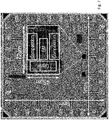
- Fig. 7 shows a die micrograph with inset showing a zoomed-in version of the asynchronous flipping ADC.
- the ADC core occupies only 45x72 ⁇ m 2 (0.0032mm 2 ). No calibration is required and no complex post-processing is used for reconstruction.
- the output spectrum can consist of the signal and its first-order-shaped odd harmonics.
- First-order quantization error shaping can result in high-power out-of-band quantization spectral components and can attenuate such components at low, in-band, frequencies.
- the noise and distortion power was integrated over the 10MHz-50MHz BW, resulting in 32dB-42dB SNDR, which is sufficient for ultra-low-power applications like wake-up receivers.
- the total power dissipation, including the power of the threshold-setting scheme, is 24 ⁇ W, resulting in a Figure of Merit (FoM) of 3-10fJ/conv-step over the BW.
- the constant input amplitude can result in constant power dissipation across the BW.
- the measured maximum output data rate was a 200MS/s.
- the threshold, Vc, (or I GM ) can be programmed, at the expense of power, to maintain an SFDR>30dB over a wide amplitude range, as illustrated in Fig. 9 , potentially easing the IF AGC in a receiver.
- Power dissipation can decrease with decreasing signal amplitude, which can confirm the event-driven operation of the asynchronous flipping ADC.
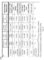
- Table 1000 compares different metrics of various prior art ADCs with the proposed asynchronous flipping ADC.
- the metrics include: technology node, power supply, input bandwidth, sampling rate, core area, SNDR, total power, and FoM.
- Fig. 13 shows a clock-less CT bandpass FIR filter 1300.
- the FIR filter can have asynchronous delay and adder blocks. Its estimated power dissipation is: E DSP x (# of taps) x [V IN,pp x ⁇ 0 /V c ], where E DSP is the DSP energy per sample per tap and ⁇ 0 is the G m -C UGB (75MHz). For an 8-tap FIR, which gives 30dB rejection, the estimated worst-case power dissipation can be 20 ⁇ W. Thus, the ADC power efficiency can be carried over to the DSP as well, because of its low output data rate.
Landscapes
- Engineering & Computer Science (AREA)
- Theoretical Computer Science (AREA)
- Physics & Mathematics (AREA)
- Nonlinear Science (AREA)
- Compression, Expansion, Code Conversion, And Decoders (AREA)
- Analogue/Digital Conversion (AREA)
Claims (16)
- Eine Vorrichtung, die Folgendes aufweist:eine Integratorschaltung (202, 204) mit zwei Integratoreingängen und zwei Integratorausgängen;einen ersten Schaltkreis (206, 208, 210, 212), der konfiguriert ist zum selektiven Koppeln von einem aus einem ersten Vorrichtungseingangssignal (VINP) und einem zweiten Vorrichtungseingangssignal (VINM) mit einem von einem ersten Integratoreingang und einem zweiten Integratoreingang, wobei der erste Schaltkreis Folgendes aufweist:einen ersten Schalter (206), der konfiguriert ist zum Koppeln des ersten Integratoreingangs mit dem ersten Vorrichtungseingangssignal (VINP);einen zweiten Schalter (208), der konfiguriert ist zum Koppeln des zweiten Integratoreingangs mit dem ersten Vorrichtungseingangssignal (VINP);einen dritten Schalter (210), der konfiguriert ist zum Koppeln des ersten Integratoreingangs mit dem zweiten Vorrichtungseingangssignal (VINM); undeinen vierten Schalter (212), der konfiguriert ist zum Koppeln des zweiten Integratoreingangs mit dem zweiten Vorrichtungseingangssignal (VINM);einen ersten Komparator (214), der konfiguriert ist zum:Empfangen einer ersten Ausgabe (VINP_COMP) der Integratorschaltung (202, 204) und eines erstes Referenzsignals (VTH); undErzeugen eines ersten Komparatorausgangssignals (INC); und einen zweiten Komparator (216), der konfiguriert ist zum:Empfangen einer zweiten Ausgabe (VINM_COMP) der Integratorschaltung (202, 204) und des ersten Referenzsignals (VTH); undErzeugen eines zweiten Komparatorausgangssignals (DEC), undeine Schaltsteuererzeugungsschaltung (218), die konfiguriert ist zum Empfangen des ersten und des zweiten Komparatorausgangssignals (INC, DEC) und zum Erzeugen von Steuersignalen für den ersten Schaltkreis (206, 208, 210, 212).
- Vorrichtung nach Anspruch 1, die ferner einen zweiten Schaltkreis (218) aufweist, der konfiguriert ist zum selektiven Koppeln entweder einer ersten Vorrichtungsausgabe (INC_korrigiert) oder einer zweiten Vorrichtungsausgabe (DEC_korrigiert) mit dem ersten Komparatorausgangssignal (INC) oder dem zweiten Komparatorausgangssignal (DEC), wobei der zweite Schaltkreis Folgendes aufweisteinen fünften Schalter, der konfiguriert ist zum Koppeln der ersten Vorrichtungsausgabe (INC_korrigiert) mit dem ersten Komparatorausgangssignal (INC);einen sechsten Schalter, der konfiguriert ist zum Koppeln der zweiten Vorrichtungsausgabe (DEC_korrigiert) mit dem ersten Komparatorausgangssignal (INC);einen siebten Schalter, der konfiguriert ist zum Koppeln der ersten Vorrichtungsausgabe (INC_korrigiert) mit dem zweiten Komparatorausgangssignal (DEC); undeinen achten Schalter, der konfiguriert ist zum Koppeln der zweiten Vorrichtungsausgabe (DEC_korrigiert) mit dem zweiten Komparatorausgangssignal (DEC).
- Die Vorrichtung nach Anspruch 1 oder 2, die ferner Folgendes aufweist einen dritten Komparator (402), der konfiguriert ist zum:Empfangen der ersten Ausgabe (VINP_COMP) der Integratorschaltung (202, 204) und eines zweiten Referenzsignals (VSAT); undErzeugen eines dritten Komparatorausgangssignals (INC_OVF); und einen vierten Komparator (404), der konfiguriert ist zum:Empfangen der zweiten Ausgabe (VINM_COMP) der Integratorschaltung (202, 204) und des zweiten Referenzsignals (VSAT) zu; undErzeugen eines vierten Komparatorausgangssignals (DEC_OVF).
- Vorrichtung nach Anspruch 3, die ferner ein erstes Logikgatter (412) aufweist, das konfiguriert ist zum:Empfangen des dritten Komparatorausgangssignals (INC_OVF) und des vierten Komparatorausgangssignals (DEC_OVF); undErzeugen eines Ausgangssignals (INT_RST), das auf dem dritten Komparatorausgangssignal (INC_OVF) und/oder dem vierten Komparatorausgangssignal (DEC_OVF) basiert;wobei das Ausgangssignal (INT_RST) des ersten Logikgatters (412) mit der Integratorschaltung (202, 204) gekoppelt ist; undwobei die Integratorschaltung (202, 204) konfiguriert ist zum Zurücksetzen der ersten Ausgabe (VINP_COMP) der Integratorschaltung und der zweiten Ausgabe (VINM_COMP) der Integratorschaltung ansprechend auf das Ausgangssignal (INT_RST) des ersten Logikgatters (412).
- Vorrichtung nach Anspruch 3, wobei die Schaltsteuererzeugungsschaltung ferner Folgendes aufweist:ein zweites Logikgatter, das konfiguriert ist zum:Empfangen des ersten Komparatorausgangssignals (INC) und des zweiten Komparatorausgangssignals (DEC); undErzeugen eines Ausgangssignals, das auf dem ersten Komparatorausgangssignal (INC) und/oder dem zweiten Komparatorausgangssignal (DEC) basiert;ein Flip-Flop, das konfiguriert ist zum:Empfangen des Ausgangssignals des zweiten Logikgatters; undErzeugen eines ersten Steuersignals (S) und eines zweiten Steuersignals (Ŝ); undeine erste und eine zweite Verzögerungsschaltung, die konfiguriert sind zum:
Empfangen des ersten Steuersignals (S) und des zweiten Steuersignals (Ŝ); undund ein drittes Steuersignal (SD) und ein viertes Steuersignal (ŜD) zu, wobei das dritte Steuersignal eine verzögerte Version des ersten Steuersignals ist und das vierte Steuersignal eine verzögerte Version des zweiten Steuersignals ist. - Vorrichtung nach Anspruch 5, wobei das erste Steuersignal (S) und das zweite Steuersignal (S) den ersten Schaltkreis (410) steuern; und
wobei das dritte Steuersignal (SD) und das vierte Steuersignal (SD) den zweiten Schaltkreis (416) steuern. - Vorrichtung nach einem der Ansprüche 3 bis 6, wobei mindestens einer von dem ersten Komparator (214), dem zweiten Komparator (216), dem dritten Komparator (402) und dem vierten Komparator (404) eine Offset-kompensierte inverterbasierte Schaltung aufweist.
- Vorrichtung nach einem der Ansprüche 3 bis 7, wobei eine Spannungsgröße des zweiten Referenzsignals (VSAT) das Eineinhalbfache einer Spannungsgröße des ersten Referenzsignals (VTH) beträgt.
- Asynchroner Analog-Digital-Wandler (ADC), der Folgendes aufweist:die Vorrichtung nach Anspruch 2, wobei die erste Vorrichtungsausgabe eine erste ADC-Ausgabe ist und die zweite Vorrichtungsausgabe eine zweite ADC-Ausgabe ist; undein zeitkontinuierliches Filter, das konfiguriert ist zum:Empfangen der ersten ADC-Ausgabe (INC_korrigiert) und der zweiten ADC-Ausgabe (DEC_korrigiert); undFiltern der ersten ADC-Ausgabe und der zweiten ADC-Ausgabe.
- System mit einem asynchronen Analog-Digital-Wandler (ADC), das die Vorrichtung nach einem der Ansprüche 1 bis 8 aufweist und eine Stufe zwischen einer Front-End-Schaltung (450) und einem rekonfigurierbaren, taktlosen, zeitkontinuierlichen digitalen Signalprozessor (460) bildet.
- Ein Verfahren, das Folgendes aufweist:Bereitstellen einer Integratorschaltung (202, 204) mit zwei Integratoreingängen und zwei Integratorausgängen;selektives Koppeln eines ersten Vorrichtungseingangssignals (VINP) oder eines zweiten Vorrichtungseingangssignals (VINM) mit einem ersten Integratoreingang oder einem zweiten Integratoreingang durch einen ersten Schaltkreis (206, 208, 210, 212), wobei der erste Schaltkreis Folgendes aufweist:einen ersten Schalter (206), der konfiguriert ist zum Koppeln des ersten Integratoreingangs mit dem ersten Vorrichtungseingangssignal (VINP);einen zweiten Schalter (208), der konfiguriert ist zum Koppeln des zweiten Integratoreingangs mit dem ersten Vorrichtungseingangssignal (VINP);einen dritten Schalter (210), der konfiguriert ist zum Koppeln des ersten Integratoreingangs mit dem zweiten Vorrichtungseingangssignal (VINM); undeinen vierten Schalter (212), der konfiguriert ist zum Koppeln des zweiten Integratoreingangs mit dem zweiten Vorrichtungseingangssignal (VINM);Empfangen einer ersten Ausgabe (VINP_COMP) der Integratorschaltung und eines ersten Referenzsignals (VTH) durch einen ersten Komparator (214);Erzeugen eines ersten Komparatorausgangssignals (INC) durch den ersten Komparator (214);Empfangen einer zweiten Ausgabe (VINM_COMP) der Integratorschaltung und des ersten Referenzsignals (VTH) durch einen zweiten Komparator (216);Erzeugen eines zweiten Komparatorausgangssignals (DEC) durch den zweiten Komparator (216);Empfangen des ersten und des zweiten Komparatorausgangssignals (INC, DEC) durch eine Schaltersteuererzeugungsschaltung (218); undErzeugen von Steuersignalen für den ersten Schaltkreis (206, 208, 210, 212) durch die Schaltsteuererzeugungsschaltung.
- Verfahren nach Anspruch 11, ferner aufweisend das selektive Koppeln einer ersten Vorrichtungsausgabe (INC_korrigiert) oder einer zweiten Vorrichtungsausgabe (DEC_korrigiert) mit dem ersten Komparatorausgangssignal (INC) oder dem zweiten Komparatorausgangssignal (DEC) durch einen zweiten Schaltkreis (218), wobei der zweite Schaltkreis (218) Folgendes aufweist:einen fünften Schalter, der konfiguriert ist zum Koppeln der ersten Vorrichtungsausgabe (INC_korrigiert) mit dem ersten Komparatorausgangssignal (INC);einen sechsten Schalter, der konfiguriert ist zum Koppeln der zweiten Vorrichtungsausgabe (DEC_korrigiert) mit dem ersten Komparatorausgangssignal (INC);einen siebten Schalter, der konfiguriert ist zum Koppeln der ersten Vorrichtungsausgabe (INC_korrigiert) mit dem zweiten Komparatorausgangssignal (DEC); undeinen achten Schalter, der konfiguriert ist zum Koppeln der zweiten Vorrichtungsausgabe (DEC_korrigiert) mit dem zweiten Komparatorausgangssignal (DEC).
- Verfahren nach Anspruch 11 oder 12, ferner aufweisend:Empfangen der ersten Ausgabe (VINP_COMP) der Integratorschaltung (202, 204) und eines zweiten Referenzsignals (VSAT) durch einen dritten Komparator (402);Erzeugen eines dritten Komparatorausgangssignals (INC_OVF) durch den dritten Komparator (402);Empfangen der zweiten Ausgabe (VINM_COMP) der Integratorschaltung (202, 204) und des zweiten Referenzsignals (VSAT) durch einen vierten Komparator (404); undErzeugen eines vierten Komparatorausgangssignals (DEC_OVF) durch den vierten Komparator (404).
- Verfahren nach Anspruch 13, ferner aufweisend:Empfangen des dritten Komparatorausgangssignals (INC_OVF) und des vierten Komparatorausgangssignals (DEC_OVF) durch ein erstes Logikgatter (412); undErzeugen eines Ausgangssignals (INT_RST) durch das erste Logikgatter (412), das das Ergebnis einer ODER-Verknüpfung des dritten Komparatorausgangssignals (INC_OVF) und des vierten Komparatorausgangssignals (DEC_OVF) ist;wobei das Ausgangssignal des ersten Logikgatters (412) mit der Integratorschaltung (202, 204) gekoppelt ist; undwobei die Integratorschaltung (202, 204) so konfiguriert ist, dass sie die erste Ausgabe (VINP_COMP) der Integratorschaltung und die zweite Ausgabe (VINM_COMP) der Integratorschaltung ansprechend auf das Ausgangssignal (INT_RST) des ersten Logikgatters (412) zurücksetzt.
- Verfahren nach Anspruch 13 oder 14, wobei das Verfahren weiter aufweist:Empfangen des ersten Komparatorausgangssignals (INC) und des zweiten Komparatorausgangssignals (DEC) durch ein zweites Logikgatter, das in der Schaltsteuererzeugungsschaltung enthalten ist;Erzeugen eines Ausgangssignals, das auf dem ersten Komparator-Ausgangssignal (INC) und/oder dem zweiten Komparator-Ausgangssignal (DEC) basiert, durch das zweite Logikgatter;Empfangen des Ausgangssignals des zweiten Logikgatters durch ein Flip-flop, das in der Schaltsteuerungserzeugungsschaltung enthalten ist;Erzeugen eines ersten Steuersignals (S) und eines zweiten Steuersignals (S) durch das Flip-Flop; undErzeugen eines dritten Steuersignals (SD) und eines vierten Steuersignals (ŜD), wobei das dritte Steuersignal eine verzögerte Version des ersten Steuersignals ist und das vierte Steuersignal eine verzögerte Version des zweiten Steuersignals ist;wobei das erste Steuersignal (S) und das zweite Steuersignal (S) den ersten Schaltkreis steuern; undwobei das dritte Steuersignal und das vierte Steuersignal den zweiten Schaltkreis (416) steuern.
- Verfahren nach Anspruch 12, wobei die erste Vorrichtungsausgabe eine erste ADC-Ausgabe ist und die zweite Vorrichtungsausgabe eine zweite ADC-Ausgabe ist, wobei das Verfahren ferner Folgendes aufweist:
Filtern der ersten ADC-Ausgabe und der zweiten ADC-Ausgabe durch ein zeitkontinuierliches Filter.
Applications Claiming Priority (1)
| Application Number | Priority Date | Filing Date | Title |
|---|---|---|---|
| US201462012843P | 2014-06-16 | 2014-06-16 |
Publications (2)
| Publication Number | Publication Date |
|---|---|
| EP2958236A1 EP2958236A1 (de) | 2015-12-23 |
| EP2958236B1 true EP2958236B1 (de) | 2021-12-01 |
Family
ID=53404471
Family Applications (1)
| Application Number | Title | Priority Date | Filing Date |
|---|---|---|---|
| EP15305905.0A Active EP2958236B1 (de) | 2014-06-16 | 2015-06-12 | Systeme und verfahren zur implementierung von fehlerformender, aliasfreier, asynchron umschaltender analog-digital-wandlung |
Country Status (2)
| Country | Link |
|---|---|
| US (1) | US9300315B2 (de) |
| EP (1) | EP2958236B1 (de) |
Families Citing this family (5)
| Publication number | Priority date | Publication date | Assignee | Title |
|---|---|---|---|---|
| WO2019185658A1 (en) | 2018-03-27 | 2019-10-03 | Koninklijke Philips N.V. | Systems and methods for performing analog-to-digital conversion across multiple, spatially separated stages |
| US10924128B2 (en) * | 2019-05-24 | 2021-02-16 | Analog Devices International Unlimited Company | VCO-based continuous-time pipelined ADC |
| CN111030693B (zh) * | 2019-12-06 | 2024-03-29 | 杭州微纳核芯电子科技有限公司 | 模数转换器 |
| US10965300B1 (en) * | 2020-06-12 | 2021-03-30 | Ciena Corporation | High bandwidth under-sampled successive approximation register analog to digital converter with nonlinearity minimization |
| US12191881B2 (en) * | 2022-01-10 | 2025-01-07 | Samsung Electronics Co., Ltd. | Analog-to-digital converter and analog-to-digital conversion method using the same |
Citations (2)
| Publication number | Priority date | Publication date | Assignee | Title |
|---|---|---|---|---|
| US20100214141A1 (en) * | 2009-02-24 | 2010-08-26 | Nec Electronics Corporation | Analog-to-digital converter |
| US20120169397A1 (en) * | 2010-12-30 | 2012-07-05 | Eliezer Oren E | Mixed Signal Integrator Incorporating Extended Integration Duration |
Family Cites Families (4)
| Publication number | Priority date | Publication date | Assignee | Title |
|---|---|---|---|---|
| WO2007019498A2 (en) * | 2005-08-08 | 2007-02-15 | University Of Florida Research Foundation, Inc. | Device and methods for biphasis pulse signal coding |
| US8044837B2 (en) * | 2007-03-26 | 2011-10-25 | Freescale Semiconductor, Inc. | Analogue to digital converters |
| JP2008263258A (ja) * | 2007-04-10 | 2008-10-30 | Matsushita Electric Ind Co Ltd | デルタシグマ変調回路とそれを用いたデルタシグマad変換装置 |
| EP2355358A1 (de) * | 2010-02-04 | 2011-08-10 | Nxp B.V. | Analog-digital-Wandler, Temperatursensor, kontaktfreier Transponder und Verfahren zur Umwandlung von analogen Signalen in digitale Signale |
-
2015
- 2015-06-12 EP EP15305905.0A patent/EP2958236B1/de active Active
- 2015-06-12 US US14/738,044 patent/US9300315B2/en not_active Expired - Fee Related
Patent Citations (2)
| Publication number | Priority date | Publication date | Assignee | Title |
|---|---|---|---|---|
| US20100214141A1 (en) * | 2009-02-24 | 2010-08-26 | Nec Electronics Corporation | Analog-to-digital converter |
| US20120169397A1 (en) * | 2010-12-30 | 2012-07-05 | Eliezer Oren E | Mixed Signal Integrator Incorporating Extended Integration Duration |
Also Published As
| Publication number | Publication date |
|---|---|
| US9300315B2 (en) | 2016-03-29 |
| EP2958236A1 (de) | 2015-12-23 |
| US20150365098A1 (en) | 2015-12-17 |
Similar Documents
| Publication | Publication Date | Title |
|---|---|---|
| KR101565967B1 (ko) | 시그마-델타 아날로그-디지털 변환 방법과 그 장치 | |
| US11152951B2 (en) | Quad switched multibit digital to analog converter and continuous time sigma-delta modulator | |
| US9007247B2 (en) | Multi-bit sigma-delta modulator with reduced number of bits in feedback path | |
| US8223051B2 (en) | Multi-bit sigma-delta modulator with reduced number of bits in feedback path | |
| US9300315B2 (en) | Systems and methods for implementing error-shaping alias-free asynchronous flipping analog to digital conversion | |
| TW201735548A (zh) | 用於多階噪訊移頻數位類比轉換器之適應性數位量化噪訊抵銷濾波器 | |
| US10826514B1 (en) | Noise-shaping enhanced gated ring oscillator based analog-to-digital converters | |
| Caldwell et al. | Incremental data converters at low oversampling ratios | |
| Nandi et al. | Continuous-Time $\Delta\Sigma $ Modulators With Improved Linearity and Reduced Clock Jitter Sensitivity Using the Switched-Capacitor Return-to-Zero DAC | |
| US8400340B2 (en) | Achieving high dynamic range in a sigma delta analog to digital converter | |
| JP2013042488A (ja) | 構成変更可能な連続時間シグマデルタアナログ−デジタル変換器 | |
| US9859916B1 (en) | Multistage noise shaping sigma-delta modulator | |
| JP2008263258A (ja) | デルタシグマ変調回路とそれを用いたデルタシグマad変換装置 | |
| Farag et al. | Mixed signal VLSI wireless design: circuits and systems | |
| CN102594261A (zh) | 用于抵消经调制信号的平均值的能够配置的系统 | |
| Maghari et al. | Noise-shaped integrating quantisers in ΔΣ modulators | |
| Patil et al. | A 3–10fJ/conv-step 0.0032 mm 2 error-shaping alias-free asynchronous ADC | |
| JP4901112B2 (ja) | 帯域デルタ−シグマ・アナログ−デジタル変換器 | |
| Cherry et al. | Signal-dependent timing jitter in continuous-time ΣΔ modulators | |
| Mohamed et al. | FIR feedback in continuous-time incremental sigma-delta ADCs | |
| TWI395413B (zh) | 帶通三角積分調變器 | |
| Colodro et al. | Continuous-time sigma–delta modulator with a fast tracking quantizer and reduced number of comparators | |
| KR101559456B1 (ko) | 지연된 피드―포워드 경로를 갖는 저전력·저면적 3차 시그마―델타 변조기 | |
| Assom et al. | A 4 th-Order Continuous-Time $\Delta\Sigma $ Modulator with Improved Clock Jitter Immunity using RTZ FIR DAC | |
| Tao et al. | DAC waveform effects in CT incremental ΣΔ ADCs for biosensor applications |
Legal Events
| Date | Code | Title | Description |
|---|---|---|---|
| PUAI | Public reference made under article 153(3) epc to a published international application that has entered the european phase |
Free format text: ORIGINAL CODE: 0009012 |
|
| AK | Designated contracting states |
Kind code of ref document: A1 Designated state(s): AL AT BE BG CH CY CZ DE DK EE ES FI FR GB GR HR HU IE IS IT LI LT LU LV MC MK MT NL NO PL PT RO RS SE SI SK SM TR |
|
| AX | Request for extension of the european patent |
Extension state: BA ME |
|
| 17P | Request for examination filed |
Effective date: 20160623 |
|
| RBV | Designated contracting states (corrected) |
Designated state(s): AL AT BE BG CH CY CZ DE DK EE ES FI FR GB GR HR HU IE IS IT LI LT LU LV MC MK MT NL NO PL PT RO RS SE SI SK SM TR |
|
| STAA | Information on the status of an ep patent application or granted ep patent |
Free format text: STATUS: EXAMINATION IS IN PROGRESS |
|
| 17Q | First examination report despatched |
Effective date: 20191216 |
|
| RIC1 | Information provided on ipc code assigned before grant |
Ipc: H03K 5/24 20060101ALI20210630BHEP Ipc: H03K 5/1534 20060101ALI20210630BHEP Ipc: H03M 1/60 20060101ALI20210630BHEP Ipc: H03M 1/12 20060101AFI20210630BHEP |
|
| GRAP | Despatch of communication of intention to grant a patent |
Free format text: ORIGINAL CODE: EPIDOSNIGR1 |
|
| STAA | Information on the status of an ep patent application or granted ep patent |
Free format text: STATUS: GRANT OF PATENT IS INTENDED |
|
| INTG | Intention to grant announced |
Effective date: 20210913 |
|
| GRAS | Grant fee paid |
Free format text: ORIGINAL CODE: EPIDOSNIGR3 |
|
| GRAA | (expected) grant |
Free format text: ORIGINAL CODE: 0009210 |
|
| STAA | Information on the status of an ep patent application or granted ep patent |
Free format text: STATUS: THE PATENT HAS BEEN GRANTED |
|
| AK | Designated contracting states |
Kind code of ref document: B1 Designated state(s): AL AT BE BG CH CY CZ DE DK EE ES FI FR GB GR HR HU IE IS IT LI LT LU LV MC MK MT NL NO PL PT RO RS SE SI SK SM TR |
|
| REG | Reference to a national code |
Ref country code: GB Ref legal event code: FG4D |
|
| REG | Reference to a national code |
Ref country code: AT Ref legal event code: REF Ref document number: 1452753 Country of ref document: AT Kind code of ref document: T Effective date: 20211215 Ref country code: CH Ref legal event code: EP |
|
| REG | Reference to a national code |
Ref country code: IE Ref legal event code: FG4D |
|
| REG | Reference to a national code |
Ref country code: DE Ref legal event code: R096 Ref document number: 602015075382 Country of ref document: DE |
|
| REG | Reference to a national code |
Ref country code: LT Ref legal event code: MG9D |
|
| REG | Reference to a national code |
Ref country code: NL Ref legal event code: MP Effective date: 20211201 |
|
| REG | Reference to a national code |
Ref country code: AT Ref legal event code: MK05 Ref document number: 1452753 Country of ref document: AT Kind code of ref document: T Effective date: 20211201 |
|
| PG25 | Lapsed in a contracting state [announced via postgrant information from national office to epo] |
Ref country code: RS Free format text: LAPSE BECAUSE OF FAILURE TO SUBMIT A TRANSLATION OF THE DESCRIPTION OR TO PAY THE FEE WITHIN THE PRESCRIBED TIME-LIMIT Effective date: 20211201 Ref country code: LT Free format text: LAPSE BECAUSE OF FAILURE TO SUBMIT A TRANSLATION OF THE DESCRIPTION OR TO PAY THE FEE WITHIN THE PRESCRIBED TIME-LIMIT Effective date: 20211201 Ref country code: FI Free format text: LAPSE BECAUSE OF FAILURE TO SUBMIT A TRANSLATION OF THE DESCRIPTION OR TO PAY THE FEE WITHIN THE PRESCRIBED TIME-LIMIT Effective date: 20211201 Ref country code: BG Free format text: LAPSE BECAUSE OF FAILURE TO SUBMIT A TRANSLATION OF THE DESCRIPTION OR TO PAY THE FEE WITHIN THE PRESCRIBED TIME-LIMIT Effective date: 20220301 Ref country code: AT Free format text: LAPSE BECAUSE OF FAILURE TO SUBMIT A TRANSLATION OF THE DESCRIPTION OR TO PAY THE FEE WITHIN THE PRESCRIBED TIME-LIMIT Effective date: 20211201 |
|
| PG25 | Lapsed in a contracting state [announced via postgrant information from national office to epo] |
Ref country code: SE Free format text: LAPSE BECAUSE OF FAILURE TO SUBMIT A TRANSLATION OF THE DESCRIPTION OR TO PAY THE FEE WITHIN THE PRESCRIBED TIME-LIMIT Effective date: 20211201 Ref country code: PL Free format text: LAPSE BECAUSE OF FAILURE TO SUBMIT A TRANSLATION OF THE DESCRIPTION OR TO PAY THE FEE WITHIN THE PRESCRIBED TIME-LIMIT Effective date: 20211201 Ref country code: NO Free format text: LAPSE BECAUSE OF FAILURE TO SUBMIT A TRANSLATION OF THE DESCRIPTION OR TO PAY THE FEE WITHIN THE PRESCRIBED TIME-LIMIT Effective date: 20220301 Ref country code: LV Free format text: LAPSE BECAUSE OF FAILURE TO SUBMIT A TRANSLATION OF THE DESCRIPTION OR TO PAY THE FEE WITHIN THE PRESCRIBED TIME-LIMIT Effective date: 20211201 Ref country code: HR Free format text: LAPSE BECAUSE OF FAILURE TO SUBMIT A TRANSLATION OF THE DESCRIPTION OR TO PAY THE FEE WITHIN THE PRESCRIBED TIME-LIMIT Effective date: 20211201 Ref country code: GR Free format text: LAPSE BECAUSE OF FAILURE TO SUBMIT A TRANSLATION OF THE DESCRIPTION OR TO PAY THE FEE WITHIN THE PRESCRIBED TIME-LIMIT Effective date: 20220302 Ref country code: ES Free format text: LAPSE BECAUSE OF FAILURE TO SUBMIT A TRANSLATION OF THE DESCRIPTION OR TO PAY THE FEE WITHIN THE PRESCRIBED TIME-LIMIT Effective date: 20211201 |
|
| PG25 | Lapsed in a contracting state [announced via postgrant information from national office to epo] |
Ref country code: NL Free format text: LAPSE BECAUSE OF FAILURE TO SUBMIT A TRANSLATION OF THE DESCRIPTION OR TO PAY THE FEE WITHIN THE PRESCRIBED TIME-LIMIT Effective date: 20211201 |
|
| PG25 | Lapsed in a contracting state [announced via postgrant information from national office to epo] |
Ref country code: SM Free format text: LAPSE BECAUSE OF FAILURE TO SUBMIT A TRANSLATION OF THE DESCRIPTION OR TO PAY THE FEE WITHIN THE PRESCRIBED TIME-LIMIT Effective date: 20211201 Ref country code: SK Free format text: LAPSE BECAUSE OF FAILURE TO SUBMIT A TRANSLATION OF THE DESCRIPTION OR TO PAY THE FEE WITHIN THE PRESCRIBED TIME-LIMIT Effective date: 20211201 Ref country code: RO Free format text: LAPSE BECAUSE OF FAILURE TO SUBMIT A TRANSLATION OF THE DESCRIPTION OR TO PAY THE FEE WITHIN THE PRESCRIBED TIME-LIMIT Effective date: 20211201 Ref country code: PT Free format text: LAPSE BECAUSE OF FAILURE TO SUBMIT A TRANSLATION OF THE DESCRIPTION OR TO PAY THE FEE WITHIN THE PRESCRIBED TIME-LIMIT Effective date: 20220401 Ref country code: EE Free format text: LAPSE BECAUSE OF FAILURE TO SUBMIT A TRANSLATION OF THE DESCRIPTION OR TO PAY THE FEE WITHIN THE PRESCRIBED TIME-LIMIT Effective date: 20211201 Ref country code: CZ Free format text: LAPSE BECAUSE OF FAILURE TO SUBMIT A TRANSLATION OF THE DESCRIPTION OR TO PAY THE FEE WITHIN THE PRESCRIBED TIME-LIMIT Effective date: 20211201 |
|
| REG | Reference to a national code |
Ref country code: DE Ref legal event code: R097 Ref document number: 602015075382 Country of ref document: DE |
|
| PG25 | Lapsed in a contracting state [announced via postgrant information from national office to epo] |
Ref country code: IS Free format text: LAPSE BECAUSE OF FAILURE TO SUBMIT A TRANSLATION OF THE DESCRIPTION OR TO PAY THE FEE WITHIN THE PRESCRIBED TIME-LIMIT Effective date: 20220401 |
|
| PLBE | No opposition filed within time limit |
Free format text: ORIGINAL CODE: 0009261 |
|
| STAA | Information on the status of an ep patent application or granted ep patent |
Free format text: STATUS: NO OPPOSITION FILED WITHIN TIME LIMIT |
|
| PG25 | Lapsed in a contracting state [announced via postgrant information from national office to epo] |
Ref country code: DK Free format text: LAPSE BECAUSE OF FAILURE TO SUBMIT A TRANSLATION OF THE DESCRIPTION OR TO PAY THE FEE WITHIN THE PRESCRIBED TIME-LIMIT Effective date: 20211201 Ref country code: AL Free format text: LAPSE BECAUSE OF FAILURE TO SUBMIT A TRANSLATION OF THE DESCRIPTION OR TO PAY THE FEE WITHIN THE PRESCRIBED TIME-LIMIT Effective date: 20211201 |
|
| 26N | No opposition filed |
Effective date: 20220902 |
|
| PG25 | Lapsed in a contracting state [announced via postgrant information from national office to epo] |
Ref country code: SI Free format text: LAPSE BECAUSE OF FAILURE TO SUBMIT A TRANSLATION OF THE DESCRIPTION OR TO PAY THE FEE WITHIN THE PRESCRIBED TIME-LIMIT Effective date: 20211201 |
|
| PG25 | Lapsed in a contracting state [announced via postgrant information from national office to epo] |
Ref country code: MC Free format text: LAPSE BECAUSE OF FAILURE TO SUBMIT A TRANSLATION OF THE DESCRIPTION OR TO PAY THE FEE WITHIN THE PRESCRIBED TIME-LIMIT Effective date: 20211201 |
|
| REG | Reference to a national code |
Ref country code: CH Ref legal event code: PL |
|
| REG | Reference to a national code |
Ref country code: BE Ref legal event code: MM Effective date: 20220630 |
|
| PG25 | Lapsed in a contracting state [announced via postgrant information from national office to epo] |
Ref country code: LU Free format text: LAPSE BECAUSE OF NON-PAYMENT OF DUE FEES Effective date: 20220612 Ref country code: LI Free format text: LAPSE BECAUSE OF NON-PAYMENT OF DUE FEES Effective date: 20220630 Ref country code: IE Free format text: LAPSE BECAUSE OF NON-PAYMENT OF DUE FEES Effective date: 20220612 Ref country code: CH Free format text: LAPSE BECAUSE OF NON-PAYMENT OF DUE FEES Effective date: 20220630 |
|
| PG25 | Lapsed in a contracting state [announced via postgrant information from national office to epo] |
Ref country code: IT Free format text: LAPSE BECAUSE OF FAILURE TO SUBMIT A TRANSLATION OF THE DESCRIPTION OR TO PAY THE FEE WITHIN THE PRESCRIBED TIME-LIMIT Effective date: 20211201 Ref country code: BE Free format text: LAPSE BECAUSE OF NON-PAYMENT OF DUE FEES Effective date: 20220630 |
|
| PG25 | Lapsed in a contracting state [announced via postgrant information from national office to epo] |
Ref country code: HU Free format text: LAPSE BECAUSE OF FAILURE TO SUBMIT A TRANSLATION OF THE DESCRIPTION OR TO PAY THE FEE WITHIN THE PRESCRIBED TIME-LIMIT; INVALID AB INITIO Effective date: 20150612 |
|
| PG25 | Lapsed in a contracting state [announced via postgrant information from national office to epo] |
Ref country code: MK Free format text: LAPSE BECAUSE OF FAILURE TO SUBMIT A TRANSLATION OF THE DESCRIPTION OR TO PAY THE FEE WITHIN THE PRESCRIBED TIME-LIMIT Effective date: 20211201 Ref country code: CY Free format text: LAPSE BECAUSE OF FAILURE TO SUBMIT A TRANSLATION OF THE DESCRIPTION OR TO PAY THE FEE WITHIN THE PRESCRIBED TIME-LIMIT Effective date: 20211201 |
|
| PG25 | Lapsed in a contracting state [announced via postgrant information from national office to epo] |
Ref country code: MT Free format text: LAPSE BECAUSE OF FAILURE TO SUBMIT A TRANSLATION OF THE DESCRIPTION OR TO PAY THE FEE WITHIN THE PRESCRIBED TIME-LIMIT Effective date: 20211201 |
|
| PGFP | Annual fee paid to national office [announced via postgrant information from national office to epo] |
Ref country code: DE Payment date: 20250618 Year of fee payment: 11 |
|
| PGFP | Annual fee paid to national office [announced via postgrant information from national office to epo] |
Ref country code: GB Payment date: 20250625 Year of fee payment: 11 |
|
| PGFP | Annual fee paid to national office [announced via postgrant information from national office to epo] |
Ref country code: FR Payment date: 20250623 Year of fee payment: 11 |
|
| PG25 | Lapsed in a contracting state [announced via postgrant information from national office to epo] |
Ref country code: TR Free format text: LAPSE BECAUSE OF FAILURE TO SUBMIT A TRANSLATION OF THE DESCRIPTION OR TO PAY THE FEE WITHIN THE PRESCRIBED TIME-LIMIT Effective date: 20211201 |