EP2958253A1 - Dispositif optique comprenant des composants laser à modes bloqués - Google Patents
Dispositif optique comprenant des composants laser à modes bloqués Download PDFInfo
- Publication number
- EP2958253A1 EP2958253A1 EP14305962.4A EP14305962A EP2958253A1 EP 2958253 A1 EP2958253 A1 EP 2958253A1 EP 14305962 A EP14305962 A EP 14305962A EP 2958253 A1 EP2958253 A1 EP 2958253A1
- Authority
- EP
- European Patent Office
- Prior art keywords
- optical
- mode
- optical device
- locked laser
- wavelength
- Prior art date
- Legal status (The legal status is an assumption and is not a legal conclusion. Google has not performed a legal analysis and makes no representation as to the accuracy of the status listed.)
- Withdrawn
Links
- 230000003287 optical effect Effects 0.000 title claims abstract description 297
- 210000001520 comb Anatomy 0.000 claims abstract description 47
- 238000001228 spectrum Methods 0.000 claims abstract description 44
- 238000001914 filtration Methods 0.000 claims description 22
- 238000000034 method Methods 0.000 claims description 11
- 239000002096 quantum dot Substances 0.000 claims description 4
- 239000004065 semiconductor Substances 0.000 claims description 4
- 239000004038 photonic crystal Substances 0.000 claims description 3
- 239000013307 optical fiber Substances 0.000 description 12
- 238000010586 diagram Methods 0.000 description 5
- 239000000969 carrier Substances 0.000 description 4
- 238000005562 fading Methods 0.000 description 3
- 239000000835 fiber Substances 0.000 description 2
- 238000010521 absorption reaction Methods 0.000 description 1
- 230000003321 amplification Effects 0.000 description 1
- 230000009977 dual effect Effects 0.000 description 1
- 238000003199 nucleic acid amplification method Methods 0.000 description 1
- 238000000926 separation method Methods 0.000 description 1
- 230000007704 transition Effects 0.000 description 1
Images
Classifications
-
- H—ELECTRICITY
- H04—ELECTRIC COMMUNICATION TECHNIQUE
- H04B—TRANSMISSION
- H04B10/00—Transmission systems employing electromagnetic waves other than radio-waves, e.g. infrared, visible or ultraviolet light, or employing corpuscular radiation, e.g. quantum communication
- H04B10/50—Transmitters
- H04B10/501—Structural aspects
- H04B10/506—Multiwavelength transmitters
-
- H—ELECTRICITY
- H01—ELECTRIC ELEMENTS
- H01S—DEVICES USING THE PROCESS OF LIGHT AMPLIFICATION BY STIMULATED EMISSION OF RADIATION [LASER] TO AMPLIFY OR GENERATE LIGHT; DEVICES USING STIMULATED EMISSION OF ELECTROMAGNETIC RADIATION IN WAVE RANGES OTHER THAN OPTICAL
- H01S5/00—Semiconductor lasers
- H01S5/005—Optical components external to the laser cavity, specially adapted therefor, e.g. for homogenisation or merging of the beams or for manipulating laser pulses, e.g. pulse shaping
- H01S5/0085—Optical components external to the laser cavity, specially adapted therefor, e.g. for homogenisation or merging of the beams or for manipulating laser pulses, e.g. pulse shaping for modulating the output, i.e. the laser beam is modulated outside the laser cavity
-
- H—ELECTRICITY
- H01—ELECTRIC ELEMENTS
- H01S—DEVICES USING THE PROCESS OF LIGHT AMPLIFICATION BY STIMULATED EMISSION OF RADIATION [LASER] TO AMPLIFY OR GENERATE LIGHT; DEVICES USING STIMULATED EMISSION OF ELECTROMAGNETIC RADIATION IN WAVE RANGES OTHER THAN OPTICAL
- H01S5/00—Semiconductor lasers
- H01S5/06—Arrangements for controlling the laser output parameters, e.g. by operating on the active medium
- H01S5/065—Mode locking; Mode suppression; Mode selection ; Self pulsating
- H01S5/0657—Mode locking, i.e. generation of pulses at a frequency corresponding to a roundtrip in the cavity
-
- H—ELECTRICITY
- H01—ELECTRIC ELEMENTS
- H01S—DEVICES USING THE PROCESS OF LIGHT AMPLIFICATION BY STIMULATED EMISSION OF RADIATION [LASER] TO AMPLIFY OR GENERATE LIGHT; DEVICES USING STIMULATED EMISSION OF ELECTROMAGNETIC RADIATION IN WAVE RANGES OTHER THAN OPTICAL
- H01S5/00—Semiconductor lasers
- H01S5/40—Arrangement of two or more semiconductor lasers, not provided for in groups H01S5/02 - H01S5/30
- H01S5/4012—Beam combining, e.g. by the use of fibres, gratings, polarisers, prisms
Definitions
- the present invention generally relates to the field of optical communication networks, in particular to optical signal transmitters for optical communication networks. More particularly, but not exclusively, the present invention relates to optical devices for generating a combined multi-wavelength optical signal adapted for being used in a wavelength division multiplexing optical network.
- optical signals are transmitted along optical links (typically, optical fibers) between nodes of the network.
- optical links typically, optical fibers
- each optical signal results from the digital modulation of the amplitude and/or phase of the light emitted by a light source (such as a laser) included in a transmitter of a node, at a certain wavelength, and it propagates along an optical fiber.
- a light source such as a laser
- WDM Wavelength Division Multiplexing
- a coupler typically combines all the optical signals generated from the light sources into one optical fiber.
- an optical device For example, an optical device has been proposed that generates, from one light source, a pair of two optical signals spaced by a given frequency, with one or two of them holding modulation data.
- the two separate signals propagate over fiber without fading.
- a high frequency carrier is produced in a receiver photo-detector, after the separation of the two signals and their mixing with modulation data.
- such an optical device is multiplied by the number of required pairs of light carriers.
- optical devices used in WDM systems include costly and bulky optical and electronic components.
- optical devices due to the presence of a high-power local oscillator which is electrically supplied, such optical devices involve high power consumption.
- optical comb i.e. an optical signal having a spectrum formed of a plurality of wavelengths with constant frequency spacing
- Such an optical comb can then be used in a WDM network to provide each of the WDM light carriers.
- At least two wavelength combs with a same frequency spacing are interleaved to form wavelength pairs separated by a given frequency interval, in general different from the comb frequency spacing.
- an optical device using an amplified loop modulation of a Mach-Zender modulator allowing the generation of such a WDM comb is known.
- such optical devices all include a high-power local oscillator which is electrically supplied.
- an object of this invention is to provide an optical device for generating a combined multi-wavelength optical signal having a reduced size, power consumption and cost.
- the present invention provides an optical device for generating a combined multi-wavelength optical signal, the optical device comprising:
- the optical device may include additional characteristics considered separately or combined, and notably:
- the present invention provides an optical communication network comprising at a transmitter side an optical device for generating a combined multi-wavelength optical signal as set forth above, and at a receiver side means for filtering optically the combined multi-wavelength optical signal.
- the optical communication network may include the additional feature wherein the optical communication network is a wavelength division multiplexing communication network and the filtering means comprise a wavelength division demultiplexer, said wavelength division demultiplexer being adapted for providing distinct optical signals to a plurality of receivers via a plurality of optical channels, each optical channel carrying one of said optical signals, the wavelength division demultiplexer being further adapted for selecting sets of associated wavelengths among the spectrum of the combined multi-wavelength optical signal so that each optical signal has a spectrum formed of one of said sets of associated wavelengths, the wavelengths within a given selected set of associated wavelengths being shifted.
- the optical communication network is a wavelength division multiplexing communication network and the filtering means comprise a wavelength division demultiplexer, said wavelength division demultiplexer being adapted for providing distinct optical signals to a plurality of receivers via a plurality of optical channels, each optical channel carrying one of said optical signals, the wavelength division demultiplexer being further adapted for selecting sets of associated wavelengths among the spectrum of the combined multi-wavelength optical signal so that
- this feature allows to transmit the combined multi-wavelength optical signal through a single optical fiber, thereby using effectively the broadband width of this optical fiber due to the absence of high frequency carrier modulation
- the present invention provides a method for transmitting data to a plurality of receivers through an optical communication network, the optical communication network comprising at a transmitter side an optical device for generating a combined multi-wavelength optical signal and at a receiver side means for filtering optically the combined multi-wavelength optical signal, the optical device comprising:
- the method for transmitting data allows providing simultaneously distinct optical signals to the receivers, each optical signal containing dual or more wavelengths able to produce a microwave high frequency carrier signal at the corresponding receiver.
- optical comb is intended to mean an optical signal having a spectrum formed of a plurality of wavelengths with constant frequency spacing.
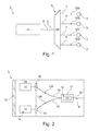
- Figure 1 shows an optical communication network 2 connected to a set of several receivers 3 via several optical channels 4.
- the optical communication network 2 comprises at a transmitter side an optical device 5 for generating a combined multi-wavelength optical signal 6 and at a receiver side means 8 for filtering optically the combined multi-wavelength optical signal 6.
- the filtering means 8 are connected to the optical device 5 thanks to an optical data link 9 comprising at least one optical fiber.
- the optical communication network 2 is a wavelength division multiplexing communication network. But this is not limited to this kind of optical communication network.
- the optical data link 9 comprises one single optical fiber.
- Each receiver 3 is for example formed of a remote antenna unit adapted to convert an electrical signal into a radioelectric signal having a given frequency.
- each remote antenna unit 3 is further adapted to emit wirelessly the radioelectric signal to a mobile terminal.
- each receiver 3 comprises a wired optical network unit connected to a remote antenna unit.
- the set of receivers 3 are connected to filtering means and connecting fibers which form a passive optical network connected to the other end of the optical device 5.
- the optical device 5 comprises at least two mode-locked laser components 10 and means 12 for superimposing optical combs 13A, 13B generated by the mode-locked laser components 10.
- the optical device 5 comprises two mode-locked laser components 10.
- the optical device 5 further comprises means 14 for modulating at least one of the optical combs 13A, 13B with base-band data.
- the optical device 5 further comprises means 16 for amplifying the generated optical combs 13A, 13B, and at least two semi-transparent mirrors 18.
- the optical device 5 comprises two semi-transparent mirrors 18.
- the optical device 5 is for example formed of a single integrated circuit.
- the optical device 5 is formed of a single photonic integrated circuit, more precisely a monolithic photonic integrated circuit.
- the optical device 5 is formed of a hybrid photonic integrated circuit.
- the mode-locked laser components 10 are equipped with one laser end mirror 15 which is attached to one end of the mode-locked laser components 10.
- Each mode-locked laser component 10 is able to generate an optical comb 13A, 13B having a spectrum formed of a plurality of wavelengths with constant frequency spacing.
- the mode-locked laser components 10 are selected so that the optical spectra of the generated optical combs 13A, 13B are shifted and the frequency spacing values of said spectra are equal.
- the optical spectra of the two generated optical combs 13A, 13B are shifted by a given frequency interval.
- each mode-locked laser component 10 is a quantum dot mode-locked laser diode. This feature allows increasing the number of wavelengths with constant frequency spacing in the spectrum of the generated optical combs 13A, 13B, as well as increasing the reproducibility of frequency spacing between the wavelengths of said generated optical combs 13A, 13B.
- each quantum dot mode-locked laser diode 10 includes an auto-pulsed laser adapted to auto-oscillate around a cavity frequency, the cavity frequency being equal to c/(2Lng) where c is the light speed, L is the cavity length and ng is an effective group refraction index of a laser waveguide.
- a mode-locked semi-conductor laser whose cavity length L is substantially equal to 400 ⁇ m will oscillate around a cavity frequency approximately equal to 100 GHz.
- the superimposing means 12 are connected to an output of each of the mode-locked laser components 10, via waveguides 19.
- the superimposing means 12 have an output 20 adapted to provide the combined multi-wavelength optical signal 6.
- the combined multi-wavelength optical signal 6 is thus formed of the superimposition of the generated optical combs 13A, 13B.
- the superimposing means 12 are formed of anoptical power combiner.
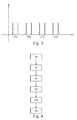
- Figure 3 illustrates the optical spectrum of the combined multi-wavelength optical signal 6. More precisely, Figure 3 illustrates the amplitude versus frequency of the combined multi-wavelength optical signal 6.
- the optical spectrum defines sets 21 A, 21 B, 21C, 21 D of associated frequencies, and hence of associated wavelengths corresponding to said frequencies.
- each set 21 A, 21 B, 21C, 21 D comprises two associated frequencies.
- the wavelengths corresponding to the frequencies within a given set 21 A, 21 B, 21C, 21 D come from the optical combs 13A, 13B generated from distinct mode-locked laser components 10, and are shifted by the frequency interval.
- the modulating means 14 are arranged within one of the mode-locked laser components 10 and are adapted for directly modulating the laser of said mode-locked laser component 10 with base-band data, under the control of an external electrical modulator. In an alternative embodiment not shown in the drawings, the modulating means 14 are arranged within each mode-locked laser component 10.
- the base-band data is advantageously in the form of an Orthogonal Frequency-Division Multiplexing (OFDM) data carried by a number of electrical frequency carriers. This notably allows carrying on a specific electrical carrier a final addressing of a signal to a mobile terminal.
- OFDM Orthogonal Frequency-Division Multiplexing
- each receiver 3 comprises a wired optical network unit connected to a remote antenna unit
- the base-band data is in the form of time slots allowing slot recognition at the corresponding optical network unit.
- the amplifying means 16 comprise an optical amplifier 24.
- the optical amplifier 24 is located within the superimposing means, namely within the optical combiner 12.
- the amplifying means 16 are separated from the superimposing means 12 and are for example connected to the output 20 of the optical combiner 12 or are arranged externally, after the output of the optical device 5.
- the optical amplifier 24 is adapted for amplifying each generated optical comb 13A, 13B.
- the optical amplifier 24 is a semiconductor optical amplifier. This allows integrating the amplifier 24 into the photonic circuit and using it to increase optical output power and to compensate for optical propagation losses of the integrated photonic circuit.
- the two semi-transparent mirrors 18 are arranged to face the laser end mirror 15 so as to form a Fabry-Perot laser optical cavity 26.
- the mode-locked laser components 10 and the modulating means 14 are arranged in the cavity 26, and the superimposing means 12 and the amplifying means 16 are arranged out of the cavity 26. This allows to ease the further combination and amplification of the generated optical combs 13A, 13B.
- each semi-transparent mirror 18 is an intra-chip mirror formed for example of a waveguide gap, or photonic crystal or Bragg gratings.
- the filtering means 8 comprise a wavelength division demultiplexer 28.
- the wavelength division demultiplexer 28 advantageously provides adequate addressing to the receivers 3.
- the filtering means 8 comprise a power splitter associated to several optical fibers, each optical fiber forming one of the optical channels 4. In this case, the optical filtering means 8 are combined with the receivers 3.
- the wavelength division demultiplexer 28 is adapted for providing distinct optical signals 30A, 30B, 30C, 30D to the receivers 3 via the optical channels 4, by filtering optically the combined multi-wavelength optical signal 6.
- the wavelength division demultiplexer 28 is further adapted for selecting each set 21 A, 21 B, 21C, 21 D of associated wavelengths among the spectrum of the combined multi-wavelength optical signal 6, so that each optical signal 30A, 30B, 30C, 30D has a spectrum formed of one of the sets 21 A, 21 B, 21C, 21 D of associated wavelengths.
- the method comprises a first step 40 during which the mode-locked laser components 10 generate at least two optical combs.
- the two mode-locked laser components 10 generate the two optical combs 13A, 13B.
- the modulating means 14 modulate at least one of the generated optical combs 13A, 13B with base-band data.
- the modulating means 14 directly modulates one comb 13B among the generated optical combs 13A, 13B with Orthogonal Frequency-Division Multiplexing data.
- the waveguides 19 transmit the generated optical combs 13A, 13B to the superimposing means 12.
- the modulation step 42 is performed in parallel of the generation step 40.
- the superimposing means 12 superimpose the generated optical combs 13A, 13B so that to form the combined multi-wavelength optical signal 6.
- the superimposing means 12 provide the combined multi-wavelength optical signal 6 on their output 20.
- the optical data link 9 transmits the combined multi-wavelength optical signal 6 to the filtering means 8.
- the filtering means 8 filter optically the combined multi-wavelength optical signal 6. More precisely, in the exemplary embodiment of Figures 1 and 2 , the wavelength division demultiplexer 28 selects the sets 21 A, 21 B, 21C, 21 D of associated wavelengths among the optical spectrum of the combined multi-wavelength optical signal 6.
- the filtering means 8 provide distinct optical signals 30A, 30B, 30C, 30D to the receivers 3 via the optical channels 4.
- Each optical signal 30A, 30B, 30C, 30D has a spectrum formed of one of the sets 21 A, 21 B, 21C, 21 D of associated wavelengths.
- each receiver 3 produces a microwave high frequency electrical carrier, the frequency of which corresponds to the frequency interval between the received wavelengths of a given set 21 A, 21 B, 21C, 21 D.
- Each receiver 3 then up-converts the base-band data contained in the corresponding optical signal 30A, 30B, 30C, 30D.
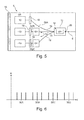
- Figure 5 illustrates a second embodiment of the optical device according to the invention wherein elements similar to the first embodiment described above are identified by identical reference numbers and thus are not described again.
- the optical device 5 comprises three mode-locked laser components 10 and three semi-transparent mirrors 18. Each mode-locked laser component 10 is able to generate an optical comb 52A, 52B, 52C having a spectrum formed of a plurality of wavelengths with constant frequency spacing.
- the mode-locked laser components 10 are selected so that the optical spectra of the generated optical combs 52A, 52B, 52C are shifted and the frequency spacing values of said spectra are equal.
- the optical spectra of the three generated optical combs 52A, 52B, 52C are shifted by two equal frequency intervals.
- the optical spectra of the three generated optical combs 52A, 52B, 52C are shifted by two different frequency intervals.
- the modulating means 14 comprise at least one optical intensity modulator 54 connected between an output of one of the mode-locked laser components 10 and the superimposing means 12.
- the or each modulator 54 is adapted for modulating the optical comb 52A, 52B, 52C generated by the corresponding mode-locked laser component 10 with base-band data, under the control of an external electrical modulator.
- the modulating means 14 comprise two modulators 54, each modulator 54 being for example formed of an electro-absorption modulator.
- the optical device 5 according to this second embodiment has an increased modulation bandwidth, due to the presence of the modulators 54.
- the optical device 5 according to this second embodiment is particularly suitable for enhanced applications such as for example compatibility with a wired passive optical network comprising several optical network units connected to remote antenna units, or in case of a multi microwave carrier wireless communication.
- Figure 6 illustrates the frequency spectrum of the combined multi-wavelength optical signal 6. More precisely, Figure 6 illustrates the amplitude versus frequency of the combined multi-wavelength optical signal 6.
- the spectrum defines sets 56A, 56B, 56C, 56D of associated frequencies, and hence of associated wavelengths corresponding to said frequencies.
- each set 56A, 56B, 56C, 56D comprises three associated frequencies.
- the wavelength corresponding to the frequencies within a given set 56A, 56B, 56C, 56D come from the optical combs 52A, 52B, 52C generated from distinct mode-locked laser components 10, and are shifted by the two frequency intervals.
- two of the three wavelengths hold the modulated optical signals coming from the generated optical combs 52B, 52C, while one of the wavelengths comes from the non-modulated optical comb 52A.
- each optical signal 30A, 30B, 30C, 30D has a spectrum formed of one of the sets 56A, 56B, 56C, 56D of associated wavelengths, and each receiver 3 produces a microwave high frequency carrier and up-converts the base-band data contained in the corresponding optical signal 30A, 30B, 30C, 30D.
- any block diagrams herein represent conceptual views of illustrative circuitry embodying the principles of the invention.
- any flow charts, flow diagrams, state transition diagrams, pseudo code, and the like represent various processes which may be substantially represented in computer readable medium and so executed by a computer or processor, whether or not such computer or processor is explicitly shown.
Landscapes
- Physics & Mathematics (AREA)
- Electromagnetism (AREA)
- Engineering & Computer Science (AREA)
- Computer Networks & Wireless Communication (AREA)
- Signal Processing (AREA)
- Optical Communication System (AREA)
Priority Applications (2)
| Application Number | Priority Date | Filing Date | Title |
|---|---|---|---|
| EP14305962.4A EP2958253A1 (fr) | 2014-06-20 | 2014-06-20 | Dispositif optique comprenant des composants laser à modes bloqués |
| PCT/EP2015/063732 WO2015193445A1 (fr) | 2014-06-20 | 2015-06-18 | Dispositif optique comprenant des composants laser à modes bloqués |
Applications Claiming Priority (1)
| Application Number | Priority Date | Filing Date | Title |
|---|---|---|---|
| EP14305962.4A EP2958253A1 (fr) | 2014-06-20 | 2014-06-20 | Dispositif optique comprenant des composants laser à modes bloqués |
Publications (1)
| Publication Number | Publication Date |
|---|---|
| EP2958253A1 true EP2958253A1 (fr) | 2015-12-23 |
Family
ID=51176992
Family Applications (1)
| Application Number | Title | Priority Date | Filing Date |
|---|---|---|---|
| EP14305962.4A Withdrawn EP2958253A1 (fr) | 2014-06-20 | 2014-06-20 | Dispositif optique comprenant des composants laser à modes bloqués |
Country Status (2)
| Country | Link |
|---|---|
| EP (1) | EP2958253A1 (fr) |
| WO (1) | WO2015193445A1 (fr) |
Cited By (2)
| Publication number | Priority date | Publication date | Assignee | Title |
|---|---|---|---|---|
| WO2018152594A1 (fr) * | 2017-02-27 | 2018-08-30 | University Of South Australia | Générateur à peigne multiples optiques, procédé de génération de peigne multiples optiques, et pluralité de lasers à mode verrouillé qui sont couplés mécaniquement et optiquement indépendants |
| US10236659B2 (en) | 2017-04-04 | 2019-03-19 | Rochester Institute Of Technology | Mode-locked lasers on silicon by palladium bonding and methods therefor |
Families Citing this family (1)
| Publication number | Priority date | Publication date | Assignee | Title |
|---|---|---|---|---|
| CN115343866A (zh) * | 2022-08-19 | 2022-11-15 | 西安邮电大学 | 一种光学频率梳生成系统 |
Citations (3)
| Publication number | Priority date | Publication date | Assignee | Title |
|---|---|---|---|---|
| US6014237A (en) * | 1998-06-01 | 2000-01-11 | Sarnoff Corporation | Multiwavelength mode-locked dense wavelength division multiplexed optical communication systems |
| US20030086449A1 (en) * | 2001-10-15 | 2003-05-08 | Alcatel | Generator of short light pulses |
| US20070133632A1 (en) * | 2005-12-08 | 2007-06-14 | Doerr Christopher R | Wide-bandwidth mode-locked laser |
-
2014
- 2014-06-20 EP EP14305962.4A patent/EP2958253A1/fr not_active Withdrawn
-
2015
- 2015-06-18 WO PCT/EP2015/063732 patent/WO2015193445A1/fr not_active Ceased
Patent Citations (3)
| Publication number | Priority date | Publication date | Assignee | Title |
|---|---|---|---|---|
| US6014237A (en) * | 1998-06-01 | 2000-01-11 | Sarnoff Corporation | Multiwavelength mode-locked dense wavelength division multiplexed optical communication systems |
| US20030086449A1 (en) * | 2001-10-15 | 2003-05-08 | Alcatel | Generator of short light pulses |
| US20070133632A1 (en) * | 2005-12-08 | 2007-06-14 | Doerr Christopher R | Wide-bandwidth mode-locked laser |
Cited By (2)
| Publication number | Priority date | Publication date | Assignee | Title |
|---|---|---|---|---|
| WO2018152594A1 (fr) * | 2017-02-27 | 2018-08-30 | University Of South Australia | Générateur à peigne multiples optiques, procédé de génération de peigne multiples optiques, et pluralité de lasers à mode verrouillé qui sont couplés mécaniquement et optiquement indépendants |
| US10236659B2 (en) | 2017-04-04 | 2019-03-19 | Rochester Institute Of Technology | Mode-locked lasers on silicon by palladium bonding and methods therefor |
Also Published As
| Publication number | Publication date |
|---|---|
| WO2015193445A1 (fr) | 2015-12-23 |
Similar Documents
| Publication | Publication Date | Title |
|---|---|---|
| Yu et al. | DWDM optical millimeter-wave generation for radio-over-fiber using an optical phase modulator and an optical interleaver | |
| US11451298B2 (en) | System and methods for distribution of heterogeneous wavelength multiplexed signals over optical access network | |
| KR100480540B1 (ko) | 광가입자단의 파장제어가 가능한 파장분할다중방식 수동형광가입자망 시스템 | |
| CN104584465B (zh) | 含有多芯光纤的空分复用装置以及自零差检波方法 | |
| EP3944014B1 (fr) | Source de lumière en peigne de fréquence optique et procédé de génération de peigne de fréquence optique | |
| US10009106B2 (en) | Silicon photonics multicarrier optical transceiver | |
| CN104094538B (zh) | 用于产生中频信号的具有鉴频器的通信装置和相关方法 | |
| US20130089333A1 (en) | Photonic integrated transmitter | |
| CN104702381B (zh) | 基于光频梳源和波分复用的mimo传输系统 | |
| KR20040040659A (ko) | 중앙 기지국에서 생성된 다파장 광의 루프백을 이용하는수동형 광통신망 | |
| JP2005130507A (ja) | 反射型利得固定半導体光増幅器を含む光信号伝送装置及びこれを用いた光通信システム | |
| CN104067540B (zh) | 用于产生中频信号的具有鉴频器和波分多路复用的通信装置和相关方法 | |
| EP1341333A2 (fr) | Longueur d'ondes modulées multiples dans un laser compact | |
| US20110182578A1 (en) | Optical Apparatus | |
| CN103248427A (zh) | 一种RoF-PON混合接入系统 | |
| US20120263474A1 (en) | Method for Arbitrary Optical Microwave and MM-Wave Generation | |
| CN115001572A (zh) | 光纤状态检测方法、光收发组件及网元设备 | |
| CN104253655B (zh) | 用于twdm‑pon的波长可调的发射器和光网络单元 | |
| JP2002270949A (ja) | 光波長分割多重信号発生装置 | |
| JP2011501618A (ja) | 光−ミリメートル波変換 | |
| WO2015193445A1 (fr) | Dispositif optique comprenant des composants laser à modes bloqués | |
| Li et al. | Generation and transmission of BB/MW/MMW signals by cascading PM and MZM | |
| US9077470B2 (en) | Optical transmission system using cross phase modulation | |
| US7848652B2 (en) | Wavelength division multiplexing passive optical network system and method of generating optical source | |
| US20090324230A1 (en) | Optical transmission system using four-wave mixing |
Legal Events
| Date | Code | Title | Description |
|---|---|---|---|
| PUAI | Public reference made under article 153(3) epc to a published international application that has entered the european phase |
Free format text: ORIGINAL CODE: 0009012 |
|
| AK | Designated contracting states |
Kind code of ref document: A1 Designated state(s): AL AT BE BG CH CY CZ DE DK EE ES FI FR GB GR HR HU IE IS IT LI LT LU LV MC MK MT NL NO PL PT RO RS SE SI SK SM TR |
|
| AX | Request for extension of the european patent |
Extension state: BA ME |
|
| 17P | Request for examination filed |
Effective date: 20160126 |
|
| RBV | Designated contracting states (corrected) |
Designated state(s): AL AT BE BG CH CY CZ DE DK EE ES FI FR GB GR HR HU IE IS IT LI LT LU LV MC MK MT NL NO PL PT RO RS SE SI SK SM TR |
|
| STAA | Information on the status of an ep patent application or granted ep patent |
Free format text: STATUS: REQUEST FOR EXAMINATION WAS MADE |
|
| STAA | Information on the status of an ep patent application or granted ep patent |
Free format text: STATUS: THE APPLICATION IS DEEMED TO BE WITHDRAWN |
|
| 18D | Application deemed to be withdrawn |
Effective date: 20180103 |