EP2959517B1 - Ensemble module photovoltaïque - Google Patents
Ensemble module photovoltaïque Download PDFInfo
- Publication number
- EP2959517B1 EP2959517B1 EP14708666.4A EP14708666A EP2959517B1 EP 2959517 B1 EP2959517 B1 EP 2959517B1 EP 14708666 A EP14708666 A EP 14708666A EP 2959517 B1 EP2959517 B1 EP 2959517B1
- Authority
- EP
- European Patent Office
- Prior art keywords
- layer
- module assembly
- photovoltaic module
- polycarbonate
- photovoltaic
- Prior art date
- Legal status (The legal status is an assumption and is not a legal conclusion. Google has not performed a legal analysis and makes no representation as to the accuracy of the status listed.)
- Active
Links
Images


Classifications
-
- H—ELECTRICITY
- H10—SEMICONDUCTOR DEVICES; ELECTRIC SOLID-STATE DEVICES NOT OTHERWISE PROVIDED FOR
- H10F—INORGANIC SEMICONDUCTOR DEVICES SENSITIVE TO INFRARED RADIATION, LIGHT, ELECTROMAGNETIC RADIATION OF SHORTER WAVELENGTH OR CORPUSCULAR RADIATION
- H10F19/00—Integrated devices, or assemblies of multiple devices, comprising at least one photovoltaic cell covered by group H10F10/00, e.g. photovoltaic modules
- H10F19/80—Encapsulations or containers for integrated devices, or assemblies of multiple devices, having photovoltaic cells
-
- H—ELECTRICITY
- H10—SEMICONDUCTOR DEVICES; ELECTRIC SOLID-STATE DEVICES NOT OTHERWISE PROVIDED FOR
- H10F—INORGANIC SEMICONDUCTOR DEVICES SENSITIVE TO INFRARED RADIATION, LIGHT, ELECTROMAGNETIC RADIATION OF SHORTER WAVELENGTH OR CORPUSCULAR RADIATION
- H10F19/00—Integrated devices, or assemblies of multiple devices, comprising at least one photovoltaic cell covered by group H10F10/00, e.g. photovoltaic modules
- H10F19/80—Encapsulations or containers for integrated devices, or assemblies of multiple devices, having photovoltaic cells
- H10F19/85—Protective back sheets
-
- H—ELECTRICITY
- H02—GENERATION; CONVERSION OR DISTRIBUTION OF ELECTRIC POWER
- H02S—GENERATION OF ELECTRIC POWER BY CONVERSION OF INFRARED RADIATION, VISIBLE LIGHT OR ULTRAVIOLET LIGHT, e.g. USING PHOTOVOLTAIC [PV] MODULES
- H02S20/00—Supporting structures for PV modules
-
- H—ELECTRICITY
- H02—GENERATION; CONVERSION OR DISTRIBUTION OF ELECTRIC POWER
- H02S—GENERATION OF ELECTRIC POWER BY CONVERSION OF INFRARED RADIATION, VISIBLE LIGHT OR ULTRAVIOLET LIGHT, e.g. USING PHOTOVOLTAIC [PV] MODULES
- H02S20/00—Supporting structures for PV modules
- H02S20/20—Supporting structures directly fixed to an immovable object
- H02S20/22—Supporting structures directly fixed to an immovable object specially adapted for buildings
- H02S20/26—Building materials integrated with PV modules, e.g. façade elements
-
- H—ELECTRICITY
- H02—GENERATION; CONVERSION OR DISTRIBUTION OF ELECTRIC POWER
- H02S—GENERATION OF ELECTRIC POWER BY CONVERSION OF INFRARED RADIATION, VISIBLE LIGHT OR ULTRAVIOLET LIGHT, e.g. USING PHOTOVOLTAIC [PV] MODULES
- H02S30/00—Structural details of PV modules other than those related to light conversion
-
- H—ELECTRICITY
- H10—SEMICONDUCTOR DEVICES; ELECTRIC SOLID-STATE DEVICES NOT OTHERWISE PROVIDED FOR
- H10F—INORGANIC SEMICONDUCTOR DEVICES SENSITIVE TO INFRARED RADIATION, LIGHT, ELECTROMAGNETIC RADIATION OF SHORTER WAVELENGTH OR CORPUSCULAR RADIATION
- H10F10/00—Individual photovoltaic cells, e.g. solar cells
-
- Y—GENERAL TAGGING OF NEW TECHNOLOGICAL DEVELOPMENTS; GENERAL TAGGING OF CROSS-SECTIONAL TECHNOLOGIES SPANNING OVER SEVERAL SECTIONS OF THE IPC; TECHNICAL SUBJECTS COVERED BY FORMER USPC CROSS-REFERENCE ART COLLECTIONS [XRACs] AND DIGESTS
- Y02—TECHNOLOGIES OR APPLICATIONS FOR MITIGATION OR ADAPTATION AGAINST CLIMATE CHANGE
- Y02B—CLIMATE CHANGE MITIGATION TECHNOLOGIES RELATED TO BUILDINGS, e.g. HOUSING, HOUSE APPLIANCES OR RELATED END-USER APPLICATIONS
- Y02B10/00—Integration of renewable energy sources in buildings
- Y02B10/10—Photovoltaic [PV]
-
- Y—GENERAL TAGGING OF NEW TECHNOLOGICAL DEVELOPMENTS; GENERAL TAGGING OF CROSS-SECTIONAL TECHNOLOGIES SPANNING OVER SEVERAL SECTIONS OF THE IPC; TECHNICAL SUBJECTS COVERED BY FORMER USPC CROSS-REFERENCE ART COLLECTIONS [XRACs] AND DIGESTS
- Y02—TECHNOLOGIES OR APPLICATIONS FOR MITIGATION OR ADAPTATION AGAINST CLIMATE CHANGE
- Y02E—REDUCTION OF GREENHOUSE GAS [GHG] EMISSIONS, RELATED TO ENERGY GENERATION, TRANSMISSION OR DISTRIBUTION
- Y02E10/00—Energy generation through renewable energy sources
- Y02E10/50—Photovoltaic [PV] energy
Definitions
- PV photovoltaic
- a PV assembly usually comprises a front sheet, generally made from a transparent or semi-transparent material such as glass, a polymer, or like materials.
- a front sheet is a glass layer
- a frame is typically required, which can generally be made of aluminum.
- the frame and the glass layer are the biggest contributors to the weight of the PV module assemblies, which can make the assemblies generally heavy and expensive to produce.
- the mechanical properties and/or the optical efficiency of the PV assembly can be decreased.
- the polymer poly(methyl methacrylate) is good for light transmission (i.e., high optical efficiency), but lacks sufficient mechanical properties.
- Polycarbonate has good mechanical properties for producing the flat sheet, but has a lower optical efficiency.
- US 2008/0223433 A1 relates to a solar module including a plurality of interconnected photovoltaic cells, an encapsulant layer encapsulating the photovoltaic cells, the encapsulant layer having a first side, a protective layer coupled to the first side of the encapsulant layer, and a stiffening layer coupled to the protective layer, the stiffening layer having an open support structure that provides stiffness to the solar module.
- PV module assemblies with one or more of increased production rates, reduced assembly times, and decreased weight, while maintaining the desired mechanical and/or electrical performance properties.
- Photovoltaic modules Disclosed, in various embodiments, are photovoltaic modules, and methods for making and using the same.
- PV module assemblies can generally comprise a frame, a junction box, cables, connectors, a ground fault circuit interrupter (GFCI), a mounting system, a tracking system, a combiner box, a back layer, encapsulant layers (e.g., ethylene vinyl acetate encapsulant layers), wafers (i.e., PV cells), an anti-reflective layer, and/or a front layer of glass.
- the frame when present, can generally be made of aluminum.
- the aluminum frame and the glass layer are the biggest contributors to the weight of the PV module assemblies, which can make the assemblies generally heavy and expensive to produce. Glass accounts for the largest part of the weight of a PV module assembly.
- the resulting PV module assembly results in a much lighter assembly (e.g., less than or equal to 10 kilograms per square meter (kg/m 2 ), specifically less than or equal to 5 kg/m 2 , for assemblies without glass as compared to 13 kg/m 2 for assemblies with glass), which can allow for placement on roofs having limited load bearing capacity (e.g., flat roofs).
- Replacing glass with plastic also generally results in a reduction in mechanical properties (e.g. stiffness and/or flexural strength) of the overall assembly. It was unexpectedly discovered that when a support layer is incorporated into the back layer, the mechanical properties of the PV module assembly could be increased without significantly increasing its weight.
- a PV module assembly (also referred to as a PV module or a PV assembly) can comprise one or more of a first layer, a photovoltaic layer comprising a photovoltaic cell and a cured composition, a back layer comprising a second layer, a support layer, and a third layer, a junction box, cables, a micro-inverter, and an optional connector connecting the first layer to the second layer.
- FIG. are merely schematic representations based on convenience and the ease of demonstrating the present disclosure, and are, therefore, not intended to indicate relative size and dimensions of the devices or components thereof and/or to define or limit the scope of the exemplary embodiments.
- FIG. 1 illustrates a schematic view of the individual components of a PV module 10, wherein the PV module 10 can comprise a first layer 12; a second layer 32 that comprises a cured composition and a PV cell 14; and a back layer 30 that comprises a second layer 32, a support layer 34, and a third layer 36.
- FIG. 1 also illustrates that the PV module 10 can comprise a connector 20 and/or 22 (20,22) that can connect the first layer 12 and the second layer 32.
- the connector 20,22 can be formed (e.g., molded) as part of either the first layer 12 or the second layer 32 or the connector 20,22 can be a separate piece, as illustrated in FIG. 1 .
- the connector 20,22 can be welded (e.g.
- the connector 20,22 can be laser welded to the second layer 32.
- the connector 20,22 can comprise any material that will provide the desired adhesion between the first layer 12 and the second layer 32, for example, the connector 20,22 can comprise an acrylic (e.g., acrylic tape or acrylic foam tape) or an acetate (e.g., ethylene vinyl acetate (EVA)) foam tape.
- the connector 20,22 can be any adhesive having sufficient structural integrity and compatibility with the first layer 12 and the second layer 32 to inhibit delamination.
- the adhesive tape can have an adhesive strength of greater than or equal to 0.1 megaPascals (MPa), or, more specifically, greater than or equal to 0.2 MPa, as determined in accordance with ISO 4587-1979 (Adhesives - Determination of tensile lap shear strength of high strength adhesive bonds).
- the elongation at break of the adhesive tape can be greater than or equal to 50%, or, more specifically, greater than or equal to 80%, or, even more specifically, greater than or equal to 95%, as measured in accordance with ISO 4587-1979 (Adhesives - Determination of tensile lap shear strength of high strength adhesive bonds).
- the connector 20,22 can act to form a gap between the first layer 12 and the second layer 32, into which a curable filling can be inserted (e.g., poured).
- the connector 20,22 can have a thickness of 0.5 to 10 millimeters (mm), or, more specifically, 1.0 to 5.0 mm, and even more specifically, 2.5 to 3.5 mm.
- the connector 20,22 can have a width that is less than or equal to 50% of a total surface area of the layer (e.g., the layer to which it is applied), or, more specifically, 1% to 40% of the total surface area, and, yet more specifically, 2% to 20% of the total surface area.
- the connector 20,22 can be located in the outer 40% of the first layer and/or the second layer (measuring from a center of the respective layer toward the edge of the respective layer), or, more specifically, in the outer 25%, and yet more specifically, in the outer 10%.
- the connector 20,22 could be located between the outer edge and 0.4 m from the outer edge, or, more specifically, between the outer edge and 0.25 m from the outer edge, and yet more specifically, between the outer edge and 0.05 m from the outer edge.
- the first layer, the second layer, and the third layer can be made of the same or different materials and can each independently comprise a polymeric material, e.g., a thermoplastic material.
- the thermoplastic material can comprise oligomers, polymers, ionomers, dendrimers, copolymers such as block copolymers, graft copolymers, star block copolymers, random copolymers, and combinations comprising at least one of the foregoing having the desired optical properties for a PV application.
- thermoplastic materials include, but are not limited to, polycarbonates (e.g., blends of polycarbonate (such as polycarbonate-polybutadiene blends), and copolycarbonates (such as copolyester-polycarbonates)), polystyrenes (e.g., copolymers of polycarbonate and styrene, acrylonitrile-styrene-butadiene copolymers, and acrylonitrile-styrene-acrylonitrile (ASA) copolymers), poly(phenylene ether)-polystyrene resins, polyalkylmethacrylates (e.g., polymethacrylates, poly(methyl methacrylates) (PMMA)), polyesters (e.g., copolyesters, polythioesters), polyolefins (e.g., polypropylenes and polyethylenes, high density polyethylenes, low density polyethylenes, linear low density polyethylenes), polyamide
- thermoplastic material used in one or more of the first layer, the second layer, or the third layer can include, but are not limited to, polycarbonate resins (e.g., LEXANTM resins, commercially available from SABIC's Innovative Plastics business, specifically LEXANTM SLX2071T or LEXANTM LUX2660T), poly(methyl methacrylate resins (e.g.
- ALTUGLASTM HT121 commercially available from ARKEMA Inc.
- polyphenylene ether-polystyrene resins and/or polyphenylene oxide resins e.g., NORYLTM resins (specifically NORYLTM 6850H or PPX7110), commercially available from SABIC's Innovative Plastics business
- polyetherimide resins e.g., ULTEMTM resins, commercially available from SABIC's innovative Plastics business
- polybutylene terephthalate-polycarbonate resins e.g., XENOYTM resins, commercially available from SABIC's innovative Plastics business
- copolyestercarbonate resins e.g.
- the first layer, the second layer and the third layer each independently comprise, but are not limited to, homopolymers and copolymers of: a polycarbonate, a polyester, a polyacrylate, a polyamide, a polyetherimide, a polyphenylene ether, or a combination comprising at least one of the foregoing resins.
- the polycarbonate can comprise copolymers of polycarbonate (e.g., polycarbonate-polysiloxane, such as polycarbonate-polysiloxane block copolymer), linear polycarbonate, branched polycarbonate, end-capped polycarbonate (e.g., nitrile end-capped polycarbonate), and combinations comprising at least one of the foregoing, for example a combination of branched and linear polycarbonate.
- polycarbonate e.g., polycarbonate-polysiloxane, such as polycarbonate-polysiloxane block copolymer
- linear polycarbonate e.g., polycarbonate-polysiloxane, such as polycarbonate-polysiloxane block copolymer
- linear polycarbonate e.g., branched polycarbonate
- end-capped polycarbonate e.g., nitrile end-capped polycarbonate
- the polycarbonate can comprise a copolymer of polycarbonate, for example a polycarbonate/acrylonitrile-styrene-acrylonitrile resin (such as GELOYTM XTPMFR15 or GELOYTMHRA222F, commercially available from SABIC's Innovative Plastics business).
- the thermoplastic resin can comprise a PA 12 resin (such as GRILAMIDTM TR90UV, available from EMS GRIVORY).
- the first layer can comprise poly(methyl methacrylate), polycarbonate, or a combination comprising one or both of the foregoing and the second and third layers can each independently comprise an acrylonitrile-styrene-acrylonitrile copolymer, a polycarbonate-acrylonitrile-styrene-acrylonitrile copolymer, poly(phenylene oxide), polypropylene, or a combination comprising one or more of the foregoing.
- the first layer can comprise poly(methyl methacrylate) and the second and third layers can comprise an acrylonitrile-styrene-acrylonitrile copolymer.
- the second and third layers can, optionally, comprise the same polymer that can be different from that of the first layer.
- One or more of the first, second, and third layers can include various additives ordinarily incorporated into polymer compositions of this type, with the proviso that the additive(s) are selected so as to not significantly adversely affect the desired properties of the PV module assembly, in particular, energy yield and weight savings.
- additives that can be included in the materials used to make the various layers of the PV module assembly include, but are not limited to, optical effects filler, impact modifiers, fillers, reinforcing agents, antioxidants, heat stabilizers, light stabilizers, ultraviolet (UV) light stabilizers, plasticizers, lubricants, mold release agents, antistatic agents, colorants (such as titanium dioxide, carbon black, inorganic dyes, and organic dyes), surface effect additives, radiation stabilizers (e.g., infrared absorbing), gamma stabilizer, flame retardants, and anti-drip agents.
- a combination of additives can be used, for example a combination of a heat stabilizer, mold release agent, and ultraviolet light stabilizer.
- the additives are used in the amounts generally known to be effective.
- Each of these additives can be present in amounts of 0.0001 to 10 weight percent (wt.%), specifically 0.001 to 5 wt.%, based on the total weight of the layer in which the additive is incorporated.
- additives can be added such that, for example, the second layer is white, for example to improve optical performance, and/or the third layer is black, for example to improve heat transfer.
- One or more of the first, second, and third layers can optionally comprise a flame retardant.
- Flame retardants include organic and/or inorganic materials.
- Organic compounds include, for example, phosphorus, sulphonates, and/or halogenated materials (e.g., comprising bromine chlorine, and so forth, such as brominated polycarbonate).
- Non-brominated and non-chlorinated phosphorus-containing flame retardant additives can be preferred in certain applications for regulatory reasons, for example organic phosphates and organic compounds containing phosphorus-nitrogen bonds.
- Inorganic flame retardants include, for example, C 1-16 alkyl sulfonate salts such as potassium perfluorobutane sulfonate (Rimar salt), potassium perfluorooctane sulfonate, tetraethyl ammonium perfluorohexane sulfonate, and potassium diphenylsulfone sulfonate (e.g., KSS); salts such as Na 2 CO 3 , K 2 CO 3 , MgCO 3 , CaCO 3 , and BaCO 3 , or fluoro-anion complexes such as Li 3 AlF 6 , BaSiF6, KBF 4 , K 3 AlF 6 , KAlF 4 , K 2 SiF 6 , and/or Na 3 AlF 6 .
- C 1-16 alkyl sulfonate salts such as potassium perfluorobutane sulfonate (Rimar salt), potassium perfluorooct
- inorganic flame retardant salts are present in amounts of 0.01 to 10 parts by weight, more specifically 0.02 to 1 parts by weight, based on 100 parts by weight of the total composition of the layer of the PV module assembly 10 in which it is included (i.e., the first layer 12, the second layer 32, or the third layer 36), excluding any filler.
- Anti-drip agents can also be used in the composition forming one or more of the first, second, and third layers, for example a fibril forming fluoropolymer such as polytetrafluoroethylene (PTFE).
- the anti-drip agent can be encapsulated by a rigid copolymer, for example styrene-acrylonitrile copolymer (SAN).
- SAN styrene-acrylonitrile copolymer
- TSAN styrene-acrylonitrile copolymer
- An exemplary TSAN comprises 50 wt.% PTFE and 50 wt.% SAN, based on the total weight of the encapsulated fluoropolymer.
- the SAN can comprise, for example, 75 wt.% styrene and 25 wt.% acrylonitrile based on the total weight of the copolymer.
- Anti-drip agents can be used in amounts of 0.1 to 10 parts by weight, based on 100 parts by weight of the total composition of the particular layer, excluding any filler.
- first, second, and third layers can additionally comprise a silicone hardcoat and/or a plasma deposition layer, for example, on the outermost surface of the first layer 12 and/or the third layer 36 to potentially ensure a 20 year lifetime span for the PV module assembly.
- the first layer can be transparent
- the second layer can be transparent, semi-transparent, or opaque
- the third layer can be opaque or semitransparent, or transparent.
- end user specifications can generally specify that the various layers satisfy a particular predetermined threshold.
- Haze values as measured by ANSI/ASTM D1003-00, can be a useful determination of the optical properties of one or more of the first, second, and third layers. The lower the haze levels, the higher the transparency of the individual layer. It can be desirable to monitor the haze levels of the various layers.
- Exemplary haze levels for the transparent first layer when measured at a thickness of 5.0 mm, can be 0% to 6%, specifically 0.5% to 4%, and more specifically 1% to 2.5%.
- Exemplary haze levels for the second layer when measured at a thickness of 5.0 mm, can be generally greater than 6%, specifically, greater than or equal to 10%.
- the first layer can have a transparency of greater than or equal to 80%, specifically, greater than or equal to 85%, more specifically, greater than or equal to 90%, even more specifically, greater than or equal to 95%, and still more specifically, greater than or equal to 99%, as measured in accordance with ASTM D1003-00, Procedure A or Procedure B, using lamp D65.
- the second and/or third layer can be semi-transparent, but can also be transparent or opaque if desired, for example, for aesthetic reasons.
- the refractive index of the first layer and the second layer can be close to (e.g., within 20%) the refractive index of the cured composition; it can also be desirable for the coefficient of thermal expansion of the first layer and the second layer to be close (e.g., within 15% of each other). Further, it can be desirable for the PV module assembly to pass the impact test requirements as set forth in UL 1703. Flame retardance as tested according to the standard of the Underwriters Laboratory 94 (UL 94) of the layers can be another factor to consider when selecting materials for the first layer, the second layer, and the third layer. For example, the UL 94 rating should desirably be V0 or greater (e.g., 5VB or 5VA).
- One or more of the first, second, and third layers can also desirably have an ultraviolet light stability of 20 years such that they retain greater than or equal to 80% of their light transmission capabilities over that 20 year period.
- Turbulent airflow which functions to cool the PV module, can be created by aerodynamic features integrated in the back layer.
- the first layer can also, optionally, be textured to decrease light reflection.
- Both the turbulent air flow and the texturing can provide higher energy yield during a PV module's lifetime under different circumstances, such as sunlight entering at an angle, high ambient temperatures, and partial shading of the PV module.
- the aerodynamic features can include, but are not limited to fins, ribs, baffles, and combinations comprising at least one of the foregoing.
- Turbulent air flow and texturing, when integrated into a PV module can reduce cost, decrease production times, and reduce the weight of the PV module as well as optimize the yield of a system during its useful lifetime.
- the back layer 30 can comprise a frame, a junction box, cables, connectors, mounting points for mounting to an external structure, and an inverter (e.g., a micro-inverter). Integration of all of these components into the back layer 30 can offer significant savings in production time, assembly time, and cost compared to a PV module where each component is produced separately and has to be assembled after production.
- an inverter e.g., a micro-inverter
- PV modules comprise a top layer made of glass that can function to impart rigidity to the module and a back layer, where the material of the back layer generally does not function to impart rigidity to the module.
- the glass top layer is 3.2 millimeters (mm) thick.
- the glass top layer can be replaced with a layer comprising a thermoplastic material that can result in significant weight savings for the PV module assembly.
- the thickness of the first layer can be 0.5 to 25 mm, specifically, 1 to 8 mm, even more specifically, 1 to 3.2 mm, specifically, 1 to 1.5 mm.
- the thickness of the first, second, and third layers can be the same or different.
- a support layer 34 can be added to the back layer 30 of a PV module 10 in order to increase the mechanical properties of the PV module when the glass top layer is replaced with a layer comprising a thermoplastic material.
- the support layer 30 is located between the second 32 and third layers 36 (see e.g., FIG. 1 ) such that the thickness of the back layer is 2 to 60 mm, specifically 5 to 40 mm, even more specifically 10 to 25 mm thick.
- a combined thickness of the second 32 and third layers 36 is less than or equal to 1 mm thick.
- the support layer 30 comprises a stiffening element configured to improve the stiffness and/or impact properties of the PV module 10.
- the stiffening element can comprise vertical stiffening element(s) 60 which extend in a z direction, horizontal stiffening element(s) 62 which extend in an x direction, diagonal stiffening element(s) 64 which extend between a z and x direction, or a combination comprising one or more of the foregoing (see FIG. 5 ).
- the stiffening element can be straight, curved, or jagged.
- the geometry formed by the stiffening elements defines the openings 38 in the support layer.
- openings can have various cross-sectional geometries (in the x-z plane) including polygonal and/or rounded, such as round, oblong, multi-sided, and combinations comprising at least one of the foregoing.
- the multi-sided cross-sectional geometry can be triagonal, quatragonal, pentagonal, hexagonal (e.g., honeycomb), heptagonal, octagonal, and the like.
- the openings 38 are defined by greater than or equal to 3 stiffening elements such that each opening has greater than or equal to 3 sides.
- the openings 38 extend in the y direction forming channels 39.
- the channels 39 extend in a direction perpendicular to the length " l " of the layers.
- the support layer can be formed of stiffening elements 24 and openings such that it has an array pattern, where the array pattern can be observed in the cross-section taken along line A-A (in the x-z plane) as illustrated in FIG. 1 .
- the array pattern can comprise a honeycomb array 40, a triangular array 42, an R6 array 44, a hexakis array 46, and the like (see FIGs. 2-5 , respectively).
- the R6 array 44 is a combination of multi-sided opening geometries (also referred to as cells), e.g., a combination of 3 sided and 6 sided geometries.
- the hexakis array 46 includes an arrangement of triangles such that 12 stiffening elements 48 extend radially from a point 50 to stiffening elements 52 to form a six sided structure 54.
- the opening density can be 10 to 1,500 or more openings per 100 square centimeters (cm 2 ), specifically, 100 to 1,000 openings per 100 cm 2 , and more specifically 150 to 700 openings per 100 cm 2 .
- a support layer will comprise greater than or equal to 10 openings, specifically, greater than or equal to 50 openings, more specifically, greater than or equal to 100 openings, and still more specifically, greater than or equal to 1,000 openings.
- the support layer 34 can comprise, for example the honeycomb THERMHEXTM core material, commercially available from ECONCORE N.V. and can be formed by a thermoforming, folding, and bonding process, extrusion, or otherwise.
- the support layer 34 can be 1 to 35 mm, specifically 4 to 16 mm, and more specifically, 5 to 15 mm thick (as measured in the y direction).
- the support layer can comprise one or more of the polymers previously described with respect to the first layer, second layer, and/or third layer, as well as one or more of the previously described additives.
- the support layer can comprise polypropylene, polyethylene, polystyrene, polyethylene terephthalate, polyamide, polycarbonate, acrylonitrile-butadiene-styrene, acrylonitrile-styrene-acrylonitrile, polyurethane, polyphenylene sulfide, polyetherimide, or a combination comprising one or more of the foregoing.
- the support layer 34 can comprise a support first side 33 and/or a support second side 35.
- the support layer 34 can further comprise a first and/or a second skin that can be bonded to the support first side 33 and/or the support second side 35 of the support layer 34.
- the skin material can be the same or different from the support layer.
- the support layer 34 can comprise openings 38 as illustrated in FIG. 2 .
- the openings 38 can be unfilled (i.e., a void space) or can be filled to provide extra support.
- the openings 38 can be filled with, for example, a foam (such as a polyurethane foam, a polyimide foam such as a polyetherimide foam for example ULTEMTM resin, a polystyrene foam such as STYROFOAMTM, a silicone foam, or a polyvinyl chloride foam).
- the openings 38 extend through the support layer 34, e.g., between the second layer 32 and the third layer 36.
- the openings can extend from the second layer 32 to the third layer 36.
- the PV layer 16 of the PV module 10 can comprise a cured composition and a PV cell 14 (see e.g., FIG. 1 ).
- the cured composition can be one that is thermally cured, cured by ultraviolet (UV) radiation, catalyst cured, or can naturally cure when one or more reactive monomers are present.
- the cured composition can comprise, for example, poly(ethylene vinyl acetate) (EVA), a curable silicone (such as a silicone thermoset elastomer (TSE), a UV curable silicone, or a room temperature vulcanize (RTV) silicone), thermoplastic materials (such as aliphatic polyurethanes and/or polyolefin ionomers), and combinations comprising at least one of the foregoing.
- the thickness of the PV layer can be 0.5 to 10 mm, specifically, 1 to 5 mm, and even more specifically, 2 to 3.5 mm.
- the thickness of the PV layer can be the same as the thickness of the connector.
- FIG. 1 illustrates that PV cells 14 can be located within the PV layer 16.
- PV cells include monocrystalline silicon, polycrystalline silicon, amorphous silicon, silicon tandem cells, copper indium gallium selenide (CIGS), cadmium telluride (CdTe), and organic cells, as well as combinations comprising at least one of the foregoing.
- the various types of cells have different demands for moisture protection varying from protection against only liquid water to highly effective protection from water vapor making the moisture barrier optional.
- a PV cell can be formed of layers of p-i-n semiconductive material.
- each layer of which can, in turn, be formed of, a semiconductor alloy material (e.g., a thin film of such alloy material).
- a p-i-n type PV device such as a solar cell, can comprise individual p-i-n type cells.
- a substrate e.g., a transparent substrate
- a substrate comprising a metallic material such as stainless steel, aluminum, tantalum, molybdenum, chrome, or metallic particles embedded within an insulator (cermets).
- a thin oxide layer and/or a series of base contacts prior to the deposition of the amorphous semiconductor alloy material.
- Each of the cells can be fabricated from a body of thin film semiconductor alloy material comprising silicon and hydrogen.
- Each of the bodies of semiconductor alloy material includes an n-type layer of semiconductor alloy material; a substantially intrinsic layer of semiconductor alloy material; and a p-type layer of semiconductor alloy material.
- the intrinsic layer can include traces of n-type or p-type dopant material without forfeiting its characteristic neutrality, hence it may be referred to as a "substantially intrinsic layer".
- p-i-n type photovoltaic cells are described, the methods and materials can also be used to produce single or multiple n-i-p type solar cells, p-n type cells or devices, Schottky barrier devices, as well as other semiconductor elements and/or devices such as diodes, memory arrays, photoresistors, photodetectors, transistors, etc.
- p-in type is defined to include any aggregation of n, i, and p layers operatively disposed to provide a photoresponsive region for generating charge carriers in response to absorption of photons of incident radiation.
- the PV cell 14 converts the light energy into electrical energy.
- Suitable bulk technology PV cells 14 include amorphous silicon cells, multicrystalline silicon cells, and monocrystalline silicon cells.
- Suitable thin film technology PV cells 14 include cadmium telluride cells, copper indium selenide cells, gallium arsenide or indium selenide cells, and copper indium gallium selenide cells.
- the PV cell is a multicrystalline silicon PV cell or a monocrystalline silicon PV cell.
- each type of PV cell has a "sweet spot", or a range of wavelengths (light energy), which it converts most efficiently into electric energy.
- the PV cell should be selected so that its sweet spot matches, as much as possible, the transmitted light through the optional coating, first layer, and cured composition combination.
- the sweet spot of a multicrystalline silicon photocell or a monocrystalline silicon PV cell is 700 nanometers to 1100 nanometers.
- the PV cell can be selected such that it can harvest UV light with a wavelength of 200 to 400 nm.
- the efficiency of a PV cell can be affected by the way the cell is produced.
- the PV cell may increase its efficiency by 1%.
- PV cells can be produced using a DISCO DAD 321 cutter (available from Disco Corporation) operating at 30,000 rpm. See also U.S. Patent No. 4,097,310 , the disclosure of which is hereby fully incorporated by reference herein.
- DISCO DAD 321 cutter available from Disco Corporation
- the size (e.g., length and width) and shape of the PV cells can vary. Shapes can include various polygonal designs such as square, rectangular, and so forth.
- the length and width can, individually be up to 200 mm, specifically, 100 mm to 175 mm.
- Exemplary sizes include 100 mm by 100 mm, 125 mm by 125 mm, 150 mm by 150 mm, 156 mm by 156 mm, 175 mm by 175 mm, and 200 mm to 200 mm, 100 mm by 175 mm, and 125 mm by 150 mm.
- the cured composition can additionally aid in transporting heat out of the PV cells to the atmosphere, resulting in higher efficiency for the PV module over time.
- the back layer can be fully integrated with other features of the PV module assembly including, but not limited to the junction box, mounting points, and micro-inverter.
- a turbulent airflow to cool the PV module can be created by aerodynamic features integrated in the back layer.
- the aerodynamic features can include, but are not limited to, fins, ribs, baffles, and combinations comprising at least one of the foregoing.
- the first layer can optionally be textured to decrease light reflection away from the PV module, thereby increasing solar absorption of the PV module. Such a design with a textured first layer and/or aerodynamic features in the back layer can allow for a higher energy yield during a PV module's lifetime under different circumstances such as sunlight that enters at an angle, high ambient temperatures, and partial shading.
- the replacement of a glass layer in a PV module can advantageously result in a decrease in the overall weight of the PV module, but can also result in a decrease in the stiffness and/or flexural strength.
- a support layer specifically a support layer as described herein comprising stiffening elements, can result in an increase in one or both of the stiffness and/or flexural strength without significantly increasing the total weight of the module.
- the first, second, and third layers can each, independently, comprise a plastic material and the back layer can additionally comprise an integrated assembly including the junction box, cables, controllers, and mounting points, meaning that the production time and assembly time of the PV module assembly can be decreased.
- the first layer comprises a plastic material, such as poly(methyl methacrylate), polycarbonate, polyamide, and combinations comprising at least one of the foregoing.
- a plastic material for the first layer can allow for the incorporation of optical textures such as Fresnel lenses to increase the amount of light captured.
- Incorporating features such as triangles on a surface of the first layer adjacent to the photovoltaic layer can capture light between the PV cells that would normally be lost.
- aerodynamic features integrated in the second layer create turbulent airflow on a surface of the second layer facing the structure to which the PV module assembly is attached (e.g., roof). The turbulent air flow can allow the PV cells to operate at lower temperatures, thus increasing the efficiency of the PV module.
- the curable composition can be selected so that the refractive index (RI) of this layer is close in value to the RI of the first layer, thus limiting the light lost between the cured composition and the first layer and further increasing the efficiency of the PV module.
- RI refractive index
- the RI of PMMA is 1.49 and the RI of a cured silicone is 1.4.
- the refractive index of the material of the first layer can be within 15% of the refractive index of the material of the curable composition.
- the overall size of the module is a function of the process used to make the module, such as injection molding.
- the overall size of the module can be, for example, 1 by 1 meter (m) or 1 by 2 m, or 1 by 6 m.
- the size of the individual PV cells in the module can be, for example, 125 by 125 mm, specifically 156 by 156 mm.
- the PV module can also comprise a first layer having a coating dispersed on the outermost surface of the first layer, e.g., a silicone hardcoat and/or a plasma coating.
- the plasma coating e.g., EXATECTM E900 coating, commercially available from EXATEC LLC
- said layer can comprise planarizing layer(s) and/or organic-inorganic composition barrier coating layer(s) which can include a silicone hardcoat and/or a plasma treatment process.
- the barrier coating (which can be graded or non-graded) can comprise a zone substantially organic in composition and a zone substantially inorganic in composition.
- organic-inorganic composition barrier coatings are described in U.S. Patent No. 7,449,246 .
- Exemplary coating compositions for the organic-inorganic barrier layer are organic, ceramic and/or inorganic materials, as well as combinations comprising at least one of the foregoing. These materials can be reaction or recombination products of reacting plasma species and are deposited onto the substrate surface.
- Organic coating materials typically comprise carbon, hydrogen, oxygen, and optionally other elements, such as sulfur, nitrogen, silicon, etc., depending on the types of reactants.
- Exemplary reactants that result in organic compositions in the coating are straight or branched alkanes, alkenes, alkynes, alcohols, aldehydes, ethers, alkylene oxides, aromatics, silicones, etc., having up to 15 carbon atoms.
- Inorganic and ceramic coating materials typically comprise oxide; nitride; carbide; boride; or combinations comprising at least one of the foregoing of elements of Groups IIA, IIIA, IVA, VA, VIA, VIIA, IB, and IIB; metals of Groups IIIB, IVB, and VB; and rare-earth metals.
- the barrier coating can have optical properties that are substantially uniform along an axis of light transmission, said axis oriented substantially perpendicular to the surface of the coating.
- silicon carbide can be deposited onto a substrate (e.g., the first, second, or third layer) by recombination of plasmas generated from silane (SiH 4 ) and an organic material, such as methane or xylene.
- SiH 4 silane
- Silicon oxycarbide can be deposited from plasmas generated from silane, methane, and oxygen or silane and propylene oxide.
- Silicon oxycarbide also can be deposited from plasmas generated from organosilicone precursors, such as tetraethoxysilane (TEOS), hexamethyldisiloxane (HMDSO), hexamethyldisilazane (HMDSN), or octamethylcyclotetrasiloxane (D4).
- TEOS tetraethoxysilane
- HMDSO hexamethyldisiloxane
- HMDSN hexamethyldisilazane
- D4 oct
- Silicon nitride can be deposited from plasmas generated from silane and ammonia.
- Aluminum oxycarbonitride can be deposited from a plasma generated from a mixture of aluminum tartrate and ammonia.
- Other combinations of reactants may be chosen to obtain a desired coating composition.
- a graded composition of the coating is obtained by changing the compositions of the reactants fed into the reactor chamber during the deposition of reaction products to form the coating.
- the barrier coating can have a transmission rate of oxygen through the barrier coating of less than or equal to 0.1 cubic centimeters per square meter-day (cm 3 /(m 2 day)), as measured at 25 degrees Celsius (°C) with a gas containing 21 volume percent (vol%) oxygen.
- the water vapor transmission can be less than 0.01 grams per square meter-day (g/(m 2 day)), as measured at 25°C and with a gas having 100% relative humidity.
- Barrier layer(s) can be applied to polymer films by various methods such as chemical vapor deposition (e.g., plasma-enhanced chemical-vapor deposition, radiofrequency plasma-enhanced chemical-vapor deposition, expanding thermal-plasma chemical-vapor deposition, electron-cyclotron-resonance plasma-enhanced chemical-vapor deposition, and inductively-coupled plasma-enhanced chemical-vapor deposition), sputtering (e.g., reactive sputtering), and so forth, as well as combinations comprising at least one of the foregoing.
- chemical vapor deposition e.g., plasma-enhanced chemical-vapor deposition, radiofrequency plasma-enhanced chemical-vapor deposition, expanding thermal-plasma chemical-vapor deposition, electron-cyclotron-resonance plasma-enhanced chemical-vapor deposition, and inductively-coupled plasma-enhanced chemical-vapor deposition
- sputtering e.g., reactive sputtering
- the planarizing layer can comprise a resin such as an epoxy based resin (cycloaliphatic resin), an acrylic based resin, a silicone resin, as well as combinations comprising at least one of the foregoing.
- a planarizing layer is a UV-cured acrylic-colloidal silica coating such as the LEXANTM HP-H UV-cured acrylic-colloidal silica coating commercially available from the Specialty Film and Sheet business unit of SABIC's Innovative Plastics business.
- the planarizing layer, and/or other coatings can further include additive(s) such as flexibilizing agent(s), adhesion promoter(s), surfactant(s), catalyst(s), as well as combinations comprising at least one of the foregoing.
- the planarizing layer thickness can be 1 nanometer (nm) to 100 micrometers ( ⁇ m). Often the planarizing layer thickness can be 100 nm to 10 ⁇ m, specifically, 500 nm to 5 ⁇ m.
- the planarizing layer can be substantially smooth and substantially defect free.
- the term "average surface roughness” R a is defined as the integral of the absolute value of the roughness profile measured over an evaluation length.
- the term “peak surface roughness” R p is the height of the highest peak in the roughness profile over the evaluation length.
- substantially smooth means the average surface roughness R a is less than or equal to 4 nm, specifically, less than or equal to 2 nm, and more specifically, less than or equal to 0.75 nm.
- the peak surface roughness R p can be less than or equal to 10 nm, specifically less than or equal to 7 nm, and more specifically, less than or equal to 5.5 nm.
- Substantially defect free means the number of point defects is less than or equal to 100 per square millimeter (/mm 2 ), specifically, less than or equal to 10/mm 2 , and more specifically, 1/mm 2 .
- first, second, and third layers can be free of a coating.
- first layer comprises poly(methyl methacrylate)
- first layer can be free of a coating.
- the PV module as a whole can be designed to meet several Underwriters Laboratory (UL) and International Electrotechnical Commission (IEC) standards. Table 1 lists the various components of the PV module assembly and the tests that the each component can be designed to meet. Table 1: PV Module Assembly Components and Standards PV Cells UL 1703, IEC 61215, IEC 61646, IEC 61730, UL 790, UL-SU 8703, IEC 61701, IEC 62108 Junction Box UL 1703, UL 746C, IEC 61730-1 Connector UL-SU 6703 GFCI UL 1741 Polymeric Materials (e.g., second layer) UL-SU 5703 Mounting System UL-SU 1703-A Tracking System UL-SU 9703 Cable for PV Cells UL 4703, UL 854 (USE-2) Combiner Box UL 1741 Inverter UL 1741, IEC 61209
- the PV cells can be designed to meet Paragraphs 7.3 and 7.4 of UL 1703 Edition 3_2008.
- Paragraph 7.3 of UL 1703 states that a polymeric substrate or superstrate shall have a thermal index, both electrical and mechanical, as determined in accordance with the Standard for Polymeric Materials - Long Term Property Evaluations, UL 746B, not less than 90°C (194°F).
- the thermal index shall not be less than 20°C (36°F) above the measured operating temperature of the material. All other polymeric materials shall have a thermal index (electrical and mechanical) 20°C above the measured operating temperature.
- the measured operating temperature is the temperature measured during the open-circuit mode for Temperature Test, Section 19, or the temperature during the short-circuit mode, whichever is greater.
- Paragraph 7.4 states that a polymeric material that serves as the outer enclosure for a module or panel that: a) is intended to be installed in a multi-module or multi-panel system; or b) has an exposed surface area greater than 10 square feet (ft 2 ) (0.93 square meters (m 2 )) or a single dimension larger than 6 feet (ft) (1.83 meters (m)) shall have a flame spread index of 100 or less as determined under the Standard Method of Test for Surface Flammability of Materials Using a Radiant Heat Energy Source, ASTM E162-2001.
- the PV module assembly can also be designed to meet the requirements set forth in Paragraph 30 of UL 1703, which describes the impact test.
- UL 1703 which describes the impact test.
- a module is impacted as described below, there shall be no accessible live parts as defined in Section 15, Accessibility of Uninsulated Live Parts. Breakage of the superstrate material is acceptable provided there are no particles larger than 1 square in 6.5 square centimeters (cm 2 ) released from their normal mounting position.
- a module or panel is to be mounted in a manner representative of its intended use, and is to be subjected to a 5 foot pound (ft-lb) (6.78 Joule (J)) impact normal to the surface resulting from a 2 inch (51 mm diameter smooth steel sphere weighing 1.18 pounds (lb) (535 grams (g)) falling through a distance of 51 inches (1.295 m).
- the module or panel is to be struck at any point considered most vulnerable.
- the sphere is to be suspended by a cord and allowed to fall as a pendulum through the vertical distance of 51 inches (1.295 m) with the direction of impact normal to the surface.
- the test is to be performed on the enclosure at 25°C (77°Farenheit (F)) and also after being cooled and maintained for 3 hours at a temperature of minus 35.0 ⁇ 2.0°C (minus 31.0 ⁇ 3.6°F).
- IEC 61215 Edition 2_2005 provides requirements for the design qualification and type approval of terrestrial photovoltaic modules appropriate for long term operation in general open air climates.
- Paragraph 10.11 of IEC 61215 provides a thermal cycling test for photovoltaic assemblies. The modules are subjected to a thermal cycling test where the temperature is cycled from -40°C ⁇ 2°C to 85°C ⁇ 2°C and each cycle is no longer than 6 hours and the total cycle time is 1,000 hours.
- the photovoltaic module assemblies disclosed herein can maintain greater than or equal to 95% of the maximum power output after being exposed to a thermal cycling of -40°C ⁇ 2°C to 85°C ⁇ 2°C for 1,000 hours.
- Paragraph 10.12 of IEC 61215 provides a humidity-freeze test to determine the ability of the module to withstand the effects of high temperature and humidity followed by sub-zero temperatures.
- the modules are subject to a cycle of 85% relative humidity ⁇ 5% for 20 minutes and a recovery time of 2 to 4 hours. Ten such cycles are performed before the module is evaluated to determine if the maximum output power has decreased greater than 5% compared to the value measured before the test. If so, the module is considered to have failed the test.
- Paragraph 10.13 of IEC 61215 provides a damp heat test carried out in a climatic chamber capable to carry out the test in accordance with IEC 60068-2-3 at conditions of 85°C ⁇ 2°C with an 85% relative humidity ⁇ 5%.
- the purpose of this test is to determine the ability of the module to withstand long term exposure to penetration of humidity by applying the conditions described above for 1,000 hours.
- the severity of this test particularly challenges the lamination process and the edge sealing from humidity. Delamination and corrosion of cell parts can be observed as a result of humidity penetration.
- IEC 61646 Edition 2_2008 provides requirements for the design qualification and type approval of terrestrial thin film photovoltaic modules appropriate for long term operation in general open air climates as defined in IEC 60721-2-1.
- IEC 62108 describes the minimum requirements for the design qualification and type approval of concentrator photovoltaic modules and assemblies appropriate for long term operation in general open air climates as defined in IEC 60721-2-1.
- IEC 61701 determines the resistance of the module to corrosion from salt mist, looking at highly corrosive wet atmospheres, such as marine environments and temporary corrosive atmospheres that are also present in places where salt is used in winter periods to melt ice formations on streets and roads.
- the PV module assembly disclosed herein can be designed to weigh approximately 5 kg/m 2 compared to 13 kg/m 2 for PV modules containing a glass first layer and/or aluminum frame.
- the layers of the PV module can be formed from a thermoplastic composition by a variety of techniques such as injection molding, extrusion, rotational molding, blow molding, and thermoforming. Forming can be accomplished by injection molding. Injection molding allows for a mass produceable module without necessitating the laminating process used in modules containing a glass first layer. As a result, the assembly time for the PV module can decrease from greater than or equal to 20 minutes to 1 minute to 5 minutes, specifically, 2 minutes to 3 minutes.
- PV module assembly can be easier and less time consuming since the PV module is lighter and as mentioned, incorporates integrated mounting points which allow for easy installation. Additionally, the use of micro-inverters can allow the system to be a plug and play without the need for a separate inverter installation step.
- the overall cost of the PV module assembly can be decreased by 10% due to the faster assembly time and shorter installation time partly because of the integration of the junction box and inverter. Overall yield of the module due, for example, to partial shading, imperfect placement of the modules, or high ambient temperature, will be higher compared to other modules, further decreasing the cost of the PV module by 20%.
- the overall yield of the module can be greater than or equal to 10% higher compared to other modules, specifically, greater than or equal to 20% higher, more specifically, greater than or equal to 25%, even more specifically, greater than or equal to 50%, and still more specifically, greater than or equal to 75% higher.
- One or more of the first, second, and third layers can be reground and reused in a new layer or structural support part.
- the PV module assemblies can be used in solar power generation applications in various manners such as building facades, on rooftops (such as a skylight or roofing tile), in highway/railroad sound barriers, greenhouses, dual purpose window glazing, and commercial buildings.
- PV module assemblies as described herein are further illustrated by the following non-limiting examples.
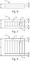
- Sample A was a solid material of a thickness t (see FIG. 6 ).
- Sample B was a back layer comprising a second layer 32, a support layer 34 with a hexagonal array stiffening element, and a third layer 36, where the thickness of the second and third layers is one half that of the thickness of the solid material of Sample A and the overall thickness of the back layer is twice that of Sample A (see FIG. 7 ).
- Sample C was a back layer comprising a second layer 32, a support layer 34 with a hexagonal array stiffening element, and a third layer 36, where the thickness of the second and third layers is one half that of the thickness of the solid material of Sample A and the overall thickness of the back layer is four times that of Sample A (see FIG. 8 ).
- the relative stiffness, the relative flexural strength, the sample weight, and the relative weight are found in Table 2, where the relative values are relative to Sample A.
- Table 2 Sample A B C Relative Stiffness 1.0 7.0 37.0 Relative Flexural Strength 1.0 3.5 9.2 Weight (pounds per square foot) 0.910 0.978 0.994 Relative Weight 1.0 1.03 1.06
- Table 2 shows the presence of the support layer results in an increase in both the stiffness and the flexural strength and that increasing the thickness of said layer results in further increases of the mechanical properties, while maintaining a low relative weight.
Landscapes
- Laminated Bodies (AREA)
- Photovoltaic Devices (AREA)
Claims (14)
- Assemblage de module photovoltaïque comprenant :une première couche (12) ;une couche arrière polymèrique (30), laquelle couche arrière comprend une deuxième couche polymèrique (32), une troisième couche polymèrique (36), et une couche de support polymèrique (34) placée entre la deuxième couche et la troisième couche, où la première couche, la deuxième couche et la troisième couche comprennent chacune indépendamment un matériau thermoplastique comprenant l'un ou les deux d'un homopolymère ou copolymère d'un polycarbonate, d'un polyester, d'un polyacrylate, d'un polyamide, d'un polyétherimide, d'un polyphénylène-éther, ou d'une combinaison comprenant au moins l'un des précédents ; etune couche photovoltaïque (16) comprenant des cellules photovoltaïques (14),dans lequel la couche photovoltaïque est située entre la première couche (12) et la couche arrière (30) ;dans lequel la couche de support (34) comprend des éléments de rigidification qui définissent des ouvertures (38) qui s'étendent dans une direction y qui est perpendiculaire à la longueur de la première couche (12) ; etdans lequel l'épaisseur combinée de la deuxième couche (32) et de la troisième couche (36) est inférieure ou égale à 1 mm.
- Assemblage de module photovoltaïque selon la revendication 1, dans lequel les éléments de rigidification comprennent un élément de rigidification vertical, un élément de rigidification horizontal, un élément de rigidification diagonal, ou une combinaison comprenant un ou plusieurs des précédents.
- Assemblage de module photovoltaïque selon l'une quelconque des revendications 1 et 2, dans lequel les éléments de rigidification comprennent un réseau en nid d'abeilles, un réseau triangulaire, un réseau R6, un réseau hexakis, ou une combinaison comprenant un ou plusieurs des précédents.
- Assemblage de module photovoltaïque selon l'une quelconque des revendications 1 à 3, dans lequel la couche de support (34) comprend des ouvertures, et dans lequel les ouvertures sont remplies.
- Assemblage de module photovoltaïque selon l'une quelconque des revendications 1 à 4, dans lequel la couche de support (34) a une épaisseur de 1 à 35 mm.
- Assemblage de module photovoltaïque selon l'une quelconque des revendications 1 à 5, dans lequel la première couche (12), la deuxième couche (32) et la troisième couche (36) comprennent chacune indépendamment un copolymère de polycarbonate, un polycarbonate linéaire, un polycarbonate ramifié, un polycarbonate coiffé en bout, ou une combinaison comprenant au moins l'un des précédents.
- Assemblage de module photovoltaïque selon l'une quelconque des revendications 1 à 6, dans lequel la première couche (12) comprend du poly(méthacrylate de méthyle), du polycarbonate, ou une combinaison comprenant l'un ou les deux des précédents.
- Assemblage de module photovoltaïque selon l'une quelconque des revendications 1 à 7, dans lequel la première couche (12) comprend du poly(méthacrylate de méthyle) et est exempte de revêtement.
- Assemblage de module photovoltaïque selon l'une quelconque des revendications 1 à 8, dans lequel l'épaisseur de la première couche (12) est de 0,5 à 25 mm.
- Assemblage de module photovoltaïque selon l'une quelconque des revendications 1 à 9, dans lequel la deuxième couche (32) et/ou la troisième couche (36) comprennent un copolymère d'acrylonitrile-styrène-acrylonitrile, un copolymère de polycarbonate-acrylonitrile-styrène-acrylonitrile, du poly(oxyde de phénylène), ou une combinaison comprenant un ou plusieurs des précédents.
- Assemblage de module photovoltaïque selon l'une quelconque des revendications 1 à 10, dans lequel la première couche (12) comprend du poly(méthacrylate de méthyle) et la deuxième couche (32) et/ou la troisième couche (36) comprennent un copolymère d'acrylonitrile-styrène-acrylonitrile.
- Assemblage de module photovoltaïque selon l'une quelconque des revendications 1 à 11, dans lequel la deuxième couche (32) et/ou la troisième couche (36) sont opaques et/ou dans lequel la deuxième couche (32) est blanche.
- Assemblage de module photovoltaïque selon l'une quelconque des revendications 1 à 12, dans lequel la troisième couche (36) est noire.
- Assemblage de module photovoltaïque selon l'une quelconque des revendications 1 à 13, dans lequel la couche photovoltaïque (16) a une épaisseur de 0,5 à 10 mm.
Applications Claiming Priority (2)
| Application Number | Priority Date | Filing Date | Title |
|---|---|---|---|
| US201361768938P | 2013-02-25 | 2013-02-25 | |
| PCT/IB2014/058821 WO2014128581A1 (fr) | 2013-02-25 | 2014-02-05 | Ensemble module photovoltaïque |
Publications (2)
| Publication Number | Publication Date |
|---|---|
| EP2959517A1 EP2959517A1 (fr) | 2015-12-30 |
| EP2959517B1 true EP2959517B1 (fr) | 2018-10-31 |
Family
ID=50238423
Family Applications (1)
| Application Number | Title | Priority Date | Filing Date |
|---|---|---|---|
| EP14708666.4A Active EP2959517B1 (fr) | 2013-02-25 | 2014-02-05 | Ensemble module photovoltaïque |
Country Status (4)
| Country | Link |
|---|---|
| US (2) | US10283661B2 (fr) |
| EP (1) | EP2959517B1 (fr) |
| CN (2) | CN110010713B (fr) |
| WO (1) | WO2014128581A1 (fr) |
Families Citing this family (19)
| Publication number | Priority date | Publication date | Assignee | Title |
|---|---|---|---|---|
| CN110010713B (zh) * | 2013-02-25 | 2020-10-27 | 沙特基础工业全球技术有限公司 | 光伏模块组件 |
| FR3043841B1 (fr) * | 2015-11-16 | 2018-09-21 | Commissariat A L'energie Atomique Et Aux Energies Alternatives | Module photovoltaique leger comportant une couche avant en verre ou polymere et une couche arriere en relief |
| FR3043840B1 (fr) * | 2015-11-16 | 2018-09-21 | Commissariat A L'energie Atomique Et Aux Energies Alternatives | Module photovoltaique leger comportant une couche avant en verre ou polymere et une couche arriere alveolaire |
| WO2017110761A1 (fr) * | 2015-12-24 | 2017-06-29 | トヨタ自動車株式会社 | Module de cellule solaire |
| CN105508974A (zh) * | 2015-12-25 | 2016-04-20 | 张宏良 | 一种太阳能灯 |
| EP3203533B1 (fr) * | 2016-02-03 | 2023-01-04 | ML SYSTEM Spólka Akcyjna | Module photovoltaïque stratifié thermiquement isolant |
| US10741703B2 (en) | 2016-07-29 | 2020-08-11 | Sunpower Corporation | Shingled solar cells overlapping along non-linear edges |
| TWI647361B (zh) * | 2016-10-05 | 2019-01-11 | 奇想創造事業股份有限公司 | Lightweight solar cell module building material and soundproof wall with the building material |
| US11362616B2 (en) * | 2017-03-06 | 2022-06-14 | Vijay Duggal | Multi-functional solar powered barrier walls and their financing methods |
| TWI634277B (zh) * | 2017-08-25 | 2018-09-01 | 徐愷陽 | 綠能建材結構改良 |
| EP3493273A1 (fr) * | 2017-12-01 | 2019-06-05 | SABIC Global Technologies B.V. | Ensemble de module photovoltaïque empilé |
| EP3712964A1 (fr) * | 2019-03-20 | 2020-09-23 | Sono Motors GmbH | Procédé de fabrication d'un module photovoltaïque |
| EP4000176A4 (fr) * | 2019-07-18 | 2023-08-16 | Palziv Ein Hanaziv Agricultural Cooperative Society Ltd. | Dispositif et système photovoltaïque |
| CN118039716A (zh) * | 2019-09-19 | 2024-05-14 | Sabic环球技术有限责任公司 | 光伏元件 |
| CA3165505A1 (fr) * | 2020-01-22 | 2021-07-29 | Nathan Peterson | Bardeaux de toiture photovoltaiques integres, procedes, systemes et kits associes |
| US11791430B2 (en) * | 2020-05-19 | 2023-10-17 | The Boeing Company | Solar panel and method for producing the solar panel |
| CN114068745B (zh) * | 2022-01-17 | 2022-05-17 | 深圳市华宝新能源股份有限公司 | 一种轻质太阳能发电板及其制备方法 |
| WO2023141566A1 (fr) | 2022-01-20 | 2023-07-27 | GAF Energy LLC | Bardeaux de toiture pour imiter l'aspect de modules photovoltaïques |
| CN119363023A (zh) * | 2024-12-23 | 2025-01-24 | 远东幕墙(珠海)有限公司 | 多功能区域化光伏组件及其划分方法、装置、设备及介质 |
Family Cites Families (32)
| Publication number | Priority date | Publication date | Assignee | Title |
|---|---|---|---|---|
| US4097310A (en) | 1975-06-03 | 1978-06-27 | Joseph Lindmayer | Method of forming silicon solar energy cells |
| JPH065782B2 (ja) * | 1986-06-19 | 1994-01-19 | 帝人株式会社 | 太陽電池モジユ−ル |
| US5614033A (en) | 1995-08-08 | 1997-03-25 | Hughes Aircraft Company | Rigid solar panel with discrete lattice and carrier structures bonded together |
| JP3369372B2 (ja) | 1995-09-26 | 2003-01-20 | 昭和飛行機工業株式会社 | ハニカムパネルの製造方法 |
| US6005184A (en) | 1997-07-11 | 1999-12-21 | Space Systems/Loral, Inc. | Solar panels having improved heat dissipation properties |
| US8704211B2 (en) | 2004-06-30 | 2014-04-22 | General Electric Company | High integrity protective coatings |
| US7449246B2 (en) | 2004-06-30 | 2008-11-11 | General Electric Company | Barrier coatings |
| US7015640B2 (en) | 2002-09-11 | 2006-03-21 | General Electric Company | Diffusion barrier coatings having graded compositions and devices incorporating the same |
| US20070074755A1 (en) * | 2005-10-03 | 2007-04-05 | Nanosolar, Inc. | Photovoltaic module with rigidizing backplane |
| US20080223433A1 (en) * | 2007-03-14 | 2008-09-18 | Evergreen Solar, Inc. | Solar Module with a Stiffening Layer |
| JP2009032954A (ja) | 2007-07-27 | 2009-02-12 | Fuji Electric Holdings Co Ltd | 太陽電池パネル及びその製造方法 |
| CN101431115B (zh) | 2007-11-07 | 2011-05-18 | E.I.内穆尔杜邦公司 | 太阳能电池板及其制造方法 |
| US20090272436A1 (en) * | 2008-05-05 | 2009-11-05 | Osbert Hay Cheung | Non-glass photovoltaic module and methods for manufacture |
| DE102008048160A1 (de) | 2008-09-19 | 2010-04-08 | Kraussmaffei Technologies Gmbh | Verfahren und Vorrichtung zur Herstellung eines Solarmoduls |
| DE102008064355A1 (de) | 2008-12-20 | 2010-07-01 | Saint-Gobain Sekurit Deutschland Gmbh & Co. Kg | Dünnschichtsolarzelle mit Leiterbahnenelektrode |
| ES2547864T3 (es) * | 2009-01-09 | 2015-10-09 | Rohm And Haas Company | Película acrílica y lámina posterior acrílica preparada a partir de la misma |
| DE102009048000A1 (de) | 2009-10-01 | 2011-09-15 | Bayer Materialscience Ag | Verbundwerkstoff aus offenzelligem Hartschaum |
| DE102009047906A1 (de) * | 2009-10-01 | 2011-04-07 | Bayer Materialscience Ag | Herstellung von Solarmodulen |
| EP2308679A1 (fr) | 2009-10-06 | 2011-04-13 | Bayer MaterialScience AG | Module solaire doté d'un film écran de polycarbonate comme film à parois arrière |
| KR20110126383A (ko) | 2010-05-17 | 2011-11-23 | 미리넷솔라 주식회사 | 솔라 셀이 구비된 하중 지지용 샌드위치 패널 및 벤치 |
| US20130056065A1 (en) * | 2010-06-07 | 2013-03-07 | E I Duont De Nemours and Company | Transparent film containing tetrafluoroethylene-hexafluoropropylene copolymer and having an organosilane coupling agent treated surface |
| TW201205838A (en) * | 2010-06-14 | 2012-02-01 | Mitsubishi Chem Corp | Solar cell module and building material inculding the same |
| WO2011161051A2 (fr) | 2010-06-25 | 2011-12-29 | Bayer Materialscience Ag | Modules solaires à couche de plastique structurée sur la face avant |
| DE102010038869A1 (de) * | 2010-08-04 | 2012-02-23 | Robert Bosch Gmbh | Photovoltaikmodul |
| EP2617568A1 (fr) * | 2010-08-16 | 2013-07-24 | 3M Innovative Properties Company | Feuille arrière solaire à base de polyoléfine |
| US20120073629A1 (en) | 2010-09-27 | 2012-03-29 | Perfect Source Technology Corp. | Solar cell module and method of manufacturing the same |
| US8507097B2 (en) * | 2010-12-21 | 2013-08-13 | E I Du Pont De Nemours And Company | Multilayer films containing a fluorinated copolymer resin layer and a cross-linkable ionomeric encapsulant layer |
| CN103477445A (zh) * | 2011-03-22 | 2013-12-25 | 陶氏环球技术有限责任公司 | 具有柔性连接器组件的改良光伏覆盖元件 |
| CN202094162U (zh) | 2011-06-23 | 2011-12-28 | 上海精锐金属建筑系统有限公司 | 一种太阳能电池板的背板散热结构 |
| US20130014821A1 (en) * | 2011-07-14 | 2013-01-17 | Du Pont Apollo Limited | Photovoltaic module |
| US20130014808A1 (en) * | 2011-07-14 | 2013-01-17 | Sabic Innovative Plastics Ip B.V. | Photovoltaic modules and methods for making and using the same |
| CN110010713B (zh) * | 2013-02-25 | 2020-10-27 | 沙特基础工业全球技术有限公司 | 光伏模块组件 |
-
2014
- 2014-02-05 CN CN201910146006.2A patent/CN110010713B/zh active Active
- 2014-02-05 CN CN201480010476.1A patent/CN105027304A/zh active Pending
- 2014-02-05 EP EP14708666.4A patent/EP2959517B1/fr active Active
- 2014-02-05 WO PCT/IB2014/058821 patent/WO2014128581A1/fr not_active Ceased
- 2014-02-24 US US14/187,998 patent/US10283661B2/en active Active
-
2019
- 2019-03-21 US US16/360,442 patent/US20190221694A1/en not_active Abandoned
Non-Patent Citations (1)
| Title |
|---|
| None * |
Also Published As
| Publication number | Publication date |
|---|---|
| CN105027304A (zh) | 2015-11-04 |
| CN110010713A (zh) | 2019-07-12 |
| EP2959517A1 (fr) | 2015-12-30 |
| US10283661B2 (en) | 2019-05-07 |
| CN110010713B (zh) | 2020-10-27 |
| US20190221694A1 (en) | 2019-07-18 |
| US20140238468A1 (en) | 2014-08-28 |
| WO2014128581A1 (fr) | 2014-08-28 |
Similar Documents
| Publication | Publication Date | Title |
|---|---|---|
| EP2959517B1 (fr) | Ensemble module photovoltaïque | |
| US20190214516A1 (en) | Photovoltaic modules and methods for making and using the same | |
| CN101317275B (zh) | 太阳电池组件用填充材料及使用其的太阳电池组件 | |
| KR102843238B1 (ko) | 광전지 소자 | |
| US8525191B2 (en) | Optoelectronic devices and coatings therefore | |
| KR101303235B1 (ko) | 태양 전지 모듈 | |
| CN102893414B (zh) | 改进的光伏器件 | |
| KR20110084218A (ko) | 솔라 패널 컴포넌트를 위한 열 전도성 재료 | |
| US20080302030A1 (en) | Structures for Low Cost, Reliable Solar Roofing | |
| EP2695203B1 (fr) | Dispositifs optoélectroniques et revêtements pour ceux-ci, et leurs procédés de fabrication et d'utilisation | |
| Kim et al. | Recent developments of polymer-based encapsulants and backsheets for stable and high-performance silicon photovoltaic modules: Materials nanoarchitectonics and mechanisms | |
| ITTO20110849A1 (it) | Pannello fotovoltaico flessibile. | |
| JP2017153195A (ja) | 融雪機能付太陽電池モジュール | |
| WO2019105920A1 (fr) | Ensemble module photovoltaïque empilé | |
| KR102253838B1 (ko) | 태양 전지 모듈 및 이에 사용되는 후면 시트 | |
| KR101742865B1 (ko) | 광전지 모듈용 봉지재 | |
| KR101162101B1 (ko) | 태양전지용 밀봉재 및 이를 포함하는 태양전지용 밀봉 시트 | |
| ES2943469T3 (es) | Módulo fotovoltaico y composición encapsulante que tienen resistencia mejorada a la degradación inducida por potencial | |
| KR102286288B1 (ko) | 태양 전지 모듈 및 이에 사용되는 후면 시트 | |
| JP2014130857A (ja) | 太陽電池裏面保護シート用樹脂組成物 |
Legal Events
| Date | Code | Title | Description |
|---|---|---|---|
| PUAI | Public reference made under article 153(3) epc to a published international application that has entered the european phase |
Free format text: ORIGINAL CODE: 0009012 |
|
| 17P | Request for examination filed |
Effective date: 20150729 |
|
| AK | Designated contracting states |
Kind code of ref document: A1 Designated state(s): AL AT BE BG CH CY CZ DE DK EE ES FI FR GB GR HR HU IE IS IT LI LT LU LV MC MK MT NL NO PL PT RO RS SE SI SK SM TR |
|
| AX | Request for extension of the european patent |
Extension state: BA ME |
|
| DAX | Request for extension of the european patent (deleted) | ||
| STAA | Information on the status of an ep patent application or granted ep patent |
Free format text: STATUS: EXAMINATION IS IN PROGRESS |
|
| 17Q | First examination report despatched |
Effective date: 20170601 |
|
| GRAP | Despatch of communication of intention to grant a patent |
Free format text: ORIGINAL CODE: EPIDOSNIGR1 |
|
| STAA | Information on the status of an ep patent application or granted ep patent |
Free format text: STATUS: GRANT OF PATENT IS INTENDED |
|
| INTG | Intention to grant announced |
Effective date: 20170707 |
|
| RIN1 | Information on inventor provided before grant (corrected) |
Inventor name: BROUNNE, MARCEL |
|
| GRAJ | Information related to disapproval of communication of intention to grant by the applicant or resumption of examination proceedings by the epo deleted |
Free format text: ORIGINAL CODE: EPIDOSDIGR1 |
|
| STAA | Information on the status of an ep patent application or granted ep patent |
Free format text: STATUS: EXAMINATION IS IN PROGRESS |
|
| GRAJ | Information related to disapproval of communication of intention to grant by the applicant or resumption of examination proceedings by the epo deleted |
Free format text: ORIGINAL CODE: EPIDOSDIGR1 |
|
| INTC | Intention to grant announced (deleted) | ||
| INTC | Intention to grant announced (deleted) | ||
| RAP3 | Party data changed (applicant data changed or rights of an application transferred) |
Owner name: SABIC GLOBAL TECHNOLOGIES B.V. |
|
| GRAP | Despatch of communication of intention to grant a patent |
Free format text: ORIGINAL CODE: EPIDOSNIGR1 |
|
| STAA | Information on the status of an ep patent application or granted ep patent |
Free format text: STATUS: GRANT OF PATENT IS INTENDED |
|
| INTG | Intention to grant announced |
Effective date: 20180530 |
|
| GRAS | Grant fee paid |
Free format text: ORIGINAL CODE: EPIDOSNIGR3 |
|
| GRAA | (expected) grant |
Free format text: ORIGINAL CODE: 0009210 |
|
| STAA | Information on the status of an ep patent application or granted ep patent |
Free format text: STATUS: THE PATENT HAS BEEN GRANTED |
|
| AK | Designated contracting states |
Kind code of ref document: B1 Designated state(s): AL AT BE BG CH CY CZ DE DK EE ES FI FR GB GR HR HU IE IS IT LI LT LU LV MC MK MT NL NO PL PT RO RS SE SI SK SM TR |
|
| REG | Reference to a national code |
Ref country code: CH Ref legal event code: EP Ref country code: GB Ref legal event code: FG4D |
|
| REG | Reference to a national code |
Ref country code: AT Ref legal event code: REF Ref document number: 1060429 Country of ref document: AT Kind code of ref document: T Effective date: 20181115 |
|
| REG | Reference to a national code |
Ref country code: DE Ref legal event code: R096 Ref document number: 602014035051 Country of ref document: DE |
|
| REG | Reference to a national code |
Ref country code: IE Ref legal event code: FG4D |
|
| REG | Reference to a national code |
Ref country code: NL Ref legal event code: FP |
|
| REG | Reference to a national code |
Ref country code: LT Ref legal event code: MG4D |
|
| REG | Reference to a national code |
Ref country code: AT Ref legal event code: MK05 Ref document number: 1060429 Country of ref document: AT Kind code of ref document: T Effective date: 20181031 |
|
| PG25 | Lapsed in a contracting state [announced via postgrant information from national office to epo] |
Ref country code: BG Free format text: LAPSE BECAUSE OF FAILURE TO SUBMIT A TRANSLATION OF THE DESCRIPTION OR TO PAY THE FEE WITHIN THE PRESCRIBED TIME-LIMIT Effective date: 20190131 Ref country code: ES Free format text: LAPSE BECAUSE OF FAILURE TO SUBMIT A TRANSLATION OF THE DESCRIPTION OR TO PAY THE FEE WITHIN THE PRESCRIBED TIME-LIMIT Effective date: 20181031 Ref country code: LT Free format text: LAPSE BECAUSE OF FAILURE TO SUBMIT A TRANSLATION OF THE DESCRIPTION OR TO PAY THE FEE WITHIN THE PRESCRIBED TIME-LIMIT Effective date: 20181031 Ref country code: NO Free format text: LAPSE BECAUSE OF FAILURE TO SUBMIT A TRANSLATION OF THE DESCRIPTION OR TO PAY THE FEE WITHIN THE PRESCRIBED TIME-LIMIT Effective date: 20190131 Ref country code: AT Free format text: LAPSE BECAUSE OF FAILURE TO SUBMIT A TRANSLATION OF THE DESCRIPTION OR TO PAY THE FEE WITHIN THE PRESCRIBED TIME-LIMIT Effective date: 20181031 Ref country code: LV Free format text: LAPSE BECAUSE OF FAILURE TO SUBMIT A TRANSLATION OF THE DESCRIPTION OR TO PAY THE FEE WITHIN THE PRESCRIBED TIME-LIMIT Effective date: 20181031 Ref country code: HR Free format text: LAPSE BECAUSE OF FAILURE TO SUBMIT A TRANSLATION OF THE DESCRIPTION OR TO PAY THE FEE WITHIN THE PRESCRIBED TIME-LIMIT Effective date: 20181031 Ref country code: IS Free format text: LAPSE BECAUSE OF FAILURE TO SUBMIT A TRANSLATION OF THE DESCRIPTION OR TO PAY THE FEE WITHIN THE PRESCRIBED TIME-LIMIT Effective date: 20190228 Ref country code: PL Free format text: LAPSE BECAUSE OF FAILURE TO SUBMIT A TRANSLATION OF THE DESCRIPTION OR TO PAY THE FEE WITHIN THE PRESCRIBED TIME-LIMIT Effective date: 20181031 Ref country code: FI Free format text: LAPSE BECAUSE OF FAILURE TO SUBMIT A TRANSLATION OF THE DESCRIPTION OR TO PAY THE FEE WITHIN THE PRESCRIBED TIME-LIMIT Effective date: 20181031 |
|
| PG25 | Lapsed in a contracting state [announced via postgrant information from national office to epo] |
Ref country code: AL Free format text: LAPSE BECAUSE OF FAILURE TO SUBMIT A TRANSLATION OF THE DESCRIPTION OR TO PAY THE FEE WITHIN THE PRESCRIBED TIME-LIMIT Effective date: 20181031 Ref country code: GR Free format text: LAPSE BECAUSE OF FAILURE TO SUBMIT A TRANSLATION OF THE DESCRIPTION OR TO PAY THE FEE WITHIN THE PRESCRIBED TIME-LIMIT Effective date: 20190201 Ref country code: SE Free format text: LAPSE BECAUSE OF FAILURE TO SUBMIT A TRANSLATION OF THE DESCRIPTION OR TO PAY THE FEE WITHIN THE PRESCRIBED TIME-LIMIT Effective date: 20181031 Ref country code: PT Free format text: LAPSE BECAUSE OF FAILURE TO SUBMIT A TRANSLATION OF THE DESCRIPTION OR TO PAY THE FEE WITHIN THE PRESCRIBED TIME-LIMIT Effective date: 20190301 Ref country code: RS Free format text: LAPSE BECAUSE OF FAILURE TO SUBMIT A TRANSLATION OF THE DESCRIPTION OR TO PAY THE FEE WITHIN THE PRESCRIBED TIME-LIMIT Effective date: 20181031 |
|
| PG25 | Lapsed in a contracting state [announced via postgrant information from national office to epo] |
Ref country code: CZ Free format text: LAPSE BECAUSE OF FAILURE TO SUBMIT A TRANSLATION OF THE DESCRIPTION OR TO PAY THE FEE WITHIN THE PRESCRIBED TIME-LIMIT Effective date: 20181031 Ref country code: IT Free format text: LAPSE BECAUSE OF FAILURE TO SUBMIT A TRANSLATION OF THE DESCRIPTION OR TO PAY THE FEE WITHIN THE PRESCRIBED TIME-LIMIT Effective date: 20181031 Ref country code: DK Free format text: LAPSE BECAUSE OF FAILURE TO SUBMIT A TRANSLATION OF THE DESCRIPTION OR TO PAY THE FEE WITHIN THE PRESCRIBED TIME-LIMIT Effective date: 20181031 |
|
| REG | Reference to a national code |
Ref country code: DE Ref legal event code: R097 Ref document number: 602014035051 Country of ref document: DE |
|
| PG25 | Lapsed in a contracting state [announced via postgrant information from national office to epo] |
Ref country code: EE Free format text: LAPSE BECAUSE OF FAILURE TO SUBMIT A TRANSLATION OF THE DESCRIPTION OR TO PAY THE FEE WITHIN THE PRESCRIBED TIME-LIMIT Effective date: 20181031 Ref country code: SM Free format text: LAPSE BECAUSE OF FAILURE TO SUBMIT A TRANSLATION OF THE DESCRIPTION OR TO PAY THE FEE WITHIN THE PRESCRIBED TIME-LIMIT Effective date: 20181031 Ref country code: RO Free format text: LAPSE BECAUSE OF FAILURE TO SUBMIT A TRANSLATION OF THE DESCRIPTION OR TO PAY THE FEE WITHIN THE PRESCRIBED TIME-LIMIT Effective date: 20181031 Ref country code: SK Free format text: LAPSE BECAUSE OF FAILURE TO SUBMIT A TRANSLATION OF THE DESCRIPTION OR TO PAY THE FEE WITHIN THE PRESCRIBED TIME-LIMIT Effective date: 20181031 |
|
| PLBE | No opposition filed within time limit |
Free format text: ORIGINAL CODE: 0009261 |
|
| STAA | Information on the status of an ep patent application or granted ep patent |
Free format text: STATUS: NO OPPOSITION FILED WITHIN TIME LIMIT |
|
| REG | Reference to a national code |
Ref country code: CH Ref legal event code: PL |
|
| 26N | No opposition filed |
Effective date: 20190801 |
|
| PG25 | Lapsed in a contracting state [announced via postgrant information from national office to epo] |
Ref country code: SI Free format text: LAPSE BECAUSE OF FAILURE TO SUBMIT A TRANSLATION OF THE DESCRIPTION OR TO PAY THE FEE WITHIN THE PRESCRIBED TIME-LIMIT Effective date: 20181031 Ref country code: MC Free format text: LAPSE BECAUSE OF FAILURE TO SUBMIT A TRANSLATION OF THE DESCRIPTION OR TO PAY THE FEE WITHIN THE PRESCRIBED TIME-LIMIT Effective date: 20181031 Ref country code: LU Free format text: LAPSE BECAUSE OF NON-PAYMENT OF DUE FEES Effective date: 20190205 |
|
| REG | Reference to a national code |
Ref country code: BE Ref legal event code: MM Effective date: 20190228 |
|
| REG | Reference to a national code |
Ref country code: IE Ref legal event code: MM4A |
|
| PG25 | Lapsed in a contracting state [announced via postgrant information from national office to epo] |
Ref country code: CH Free format text: LAPSE BECAUSE OF NON-PAYMENT OF DUE FEES Effective date: 20190228 Ref country code: LI Free format text: LAPSE BECAUSE OF NON-PAYMENT OF DUE FEES Effective date: 20190228 |
|
| PG25 | Lapsed in a contracting state [announced via postgrant information from national office to epo] |
Ref country code: IE Free format text: LAPSE BECAUSE OF NON-PAYMENT OF DUE FEES Effective date: 20190205 |
|
| PG25 | Lapsed in a contracting state [announced via postgrant information from national office to epo] |
Ref country code: BE Free format text: LAPSE BECAUSE OF NON-PAYMENT OF DUE FEES Effective date: 20190228 |
|
| PG25 | Lapsed in a contracting state [announced via postgrant information from national office to epo] |
Ref country code: MT Free format text: LAPSE BECAUSE OF NON-PAYMENT OF DUE FEES Effective date: 20190205 |
|
| PG25 | Lapsed in a contracting state [announced via postgrant information from national office to epo] |
Ref country code: CY Free format text: LAPSE BECAUSE OF FAILURE TO SUBMIT A TRANSLATION OF THE DESCRIPTION OR TO PAY THE FEE WITHIN THE PRESCRIBED TIME-LIMIT Effective date: 20181031 |
|
| PG25 | Lapsed in a contracting state [announced via postgrant information from national office to epo] |
Ref country code: HU Free format text: LAPSE BECAUSE OF FAILURE TO SUBMIT A TRANSLATION OF THE DESCRIPTION OR TO PAY THE FEE WITHIN THE PRESCRIBED TIME-LIMIT; INVALID AB INITIO Effective date: 20140205 |
|
| PG25 | Lapsed in a contracting state [announced via postgrant information from national office to epo] |
Ref country code: MK Free format text: LAPSE BECAUSE OF FAILURE TO SUBMIT A TRANSLATION OF THE DESCRIPTION OR TO PAY THE FEE WITHIN THE PRESCRIBED TIME-LIMIT Effective date: 20181031 |
|
| P01 | Opt-out of the competence of the unified patent court (upc) registered |
Effective date: 20230529 |
|
| REG | Reference to a national code |
Ref country code: DE Ref legal event code: R079 Ref document number: 602014035051 Country of ref document: DE Free format text: PREVIOUS MAIN CLASS: H01L0031048000 Ipc: H10F0019800000 |
|
| PGFP | Annual fee paid to national office [announced via postgrant information from national office to epo] |
Ref country code: NL Payment date: 20260226 Year of fee payment: 13 |
|
| PGFP | Annual fee paid to national office [announced via postgrant information from national office to epo] |
Ref country code: GB Payment date: 20260227 Year of fee payment: 13 |
|
| PGFP | Annual fee paid to national office [announced via postgrant information from national office to epo] |
Ref country code: DE Payment date: 20260227 Year of fee payment: 13 |
|
| PGFP | Annual fee paid to national office [announced via postgrant information from national office to epo] |
Ref country code: FR Payment date: 20260225 Year of fee payment: 13 |
|
| PGFP | Annual fee paid to national office [announced via postgrant information from national office to epo] |
Ref country code: TR Payment date: 20260127 Year of fee payment: 13 |