EP2960203B1 - Vorrichtung mit einer membran auf der basis von unter zugbelastung stehendem germanium - Google Patents
Vorrichtung mit einer membran auf der basis von unter zugbelastung stehendem germanium Download PDFInfo
- Publication number
- EP2960203B1 EP2960203B1 EP15171976.2A EP15171976A EP2960203B1 EP 2960203 B1 EP2960203 B1 EP 2960203B1 EP 15171976 A EP15171976 A EP 15171976A EP 2960203 B1 EP2960203 B1 EP 2960203B1
- Authority
- EP
- European Patent Office
- Prior art keywords
- germanium
- active zone
- membrane
- optical
- electronic device
- Prior art date
- Legal status (The legal status is an assumption and is not a legal conclusion. Google has not performed a legal analysis and makes no representation as to the accuracy of the status listed.)
- Active
Links
- 239000012528 membrane Substances 0.000 title claims description 68
- GNPVGFCGXDBREM-UHFFFAOYSA-N germanium atom Chemical compound [Ge] GNPVGFCGXDBREM-UHFFFAOYSA-N 0.000 title claims description 65
- 229910052732 germanium Inorganic materials 0.000 title claims description 64
- 238000005530 etching Methods 0.000 claims description 23
- 230000003287 optical effect Effects 0.000 claims description 21
- 239000000758 substrate Substances 0.000 claims description 11
- 238000000034 method Methods 0.000 claims description 10
- XAGFODPZIPBFFR-UHFFFAOYSA-N aluminium Chemical compound [Al] XAGFODPZIPBFFR-UHFFFAOYSA-N 0.000 claims description 7
- 229910052782 aluminium Inorganic materials 0.000 claims description 7
- 238000000151 deposition Methods 0.000 claims description 7
- 239000004411 aluminium Substances 0.000 claims 1
- 238000004519 manufacturing process Methods 0.000 description 19
- VYPSYNLAJGMNEJ-UHFFFAOYSA-N Silicium dioxide Chemical compound O=[Si]=O VYPSYNLAJGMNEJ-UHFFFAOYSA-N 0.000 description 8
- 229910052814 silicon oxide Inorganic materials 0.000 description 8
- XUIMIQQOPSSXEZ-UHFFFAOYSA-N Silicon Chemical compound [Si] XUIMIQQOPSSXEZ-UHFFFAOYSA-N 0.000 description 7
- 239000000463 material Substances 0.000 description 7
- 229910052710 silicon Inorganic materials 0.000 description 7
- 239000010703 silicon Substances 0.000 description 7
- XKRFYHLGVUSROY-UHFFFAOYSA-N Argon Chemical compound [Ar] XKRFYHLGVUSROY-UHFFFAOYSA-N 0.000 description 4
- 239000011149 active material Substances 0.000 description 4
- WGTYBPLFGIVFAS-UHFFFAOYSA-M tetramethylammonium hydroxide Chemical compound [OH-].C[N+](C)(C)C WGTYBPLFGIVFAS-UHFFFAOYSA-M 0.000 description 4
- 229910052786 argon Inorganic materials 0.000 description 2
- 230000008021 deposition Effects 0.000 description 2
- 238000009826 distribution Methods 0.000 description 2
- 230000000694 effects Effects 0.000 description 2
- -1 germanium selon Chemical compound 0.000 description 2
- 239000012071 phase Substances 0.000 description 2
- 238000001020 plasma etching Methods 0.000 description 2
- 230000000750 progressive effect Effects 0.000 description 2
- 229910000577 Silicon-germanium Inorganic materials 0.000 description 1
- 241001080024 Telles Species 0.000 description 1
- 239000000956 alloy Substances 0.000 description 1
- 229910045601 alloy Inorganic materials 0.000 description 1
- PNEYBMLMFCGWSK-UHFFFAOYSA-N aluminium oxide Inorganic materials [O-2].[O-2].[O-2].[Al+3].[Al+3] PNEYBMLMFCGWSK-UHFFFAOYSA-N 0.000 description 1
- 230000000052 comparative effect Effects 0.000 description 1
- 239000013078 crystal Substances 0.000 description 1
- 230000001419 dependent effect Effects 0.000 description 1
- 230000009643 growth defect Effects 0.000 description 1
- 230000001788 irregular Effects 0.000 description 1
- 239000007791 liquid phase Substances 0.000 description 1
- 239000004038 photonic crystal Substances 0.000 description 1
- 239000011347 resin Substances 0.000 description 1
- 229920005989 resin Polymers 0.000 description 1
- 239000004065 semiconductor Substances 0.000 description 1
- 230000035945 sensitivity Effects 0.000 description 1
- 238000004088 simulation Methods 0.000 description 1
- 239000010409 thin film Substances 0.000 description 1
- 239000012808 vapor phase Substances 0.000 description 1
- 238000001039 wet etching Methods 0.000 description 1
Images


Classifications
-
- H—ELECTRICITY
- H01—ELECTRIC ELEMENTS
- H01S—DEVICES USING THE PROCESS OF LIGHT AMPLIFICATION BY STIMULATED EMISSION OF RADIATION [LASER] TO AMPLIFY OR GENERATE LIGHT; DEVICES USING STIMULATED EMISSION OF ELECTROMAGNETIC RADIATION IN WAVE RANGES OTHER THAN OPTICAL
- H01S5/00—Semiconductor lasers
- H01S5/10—Construction or shape of the optical resonator, e.g. extended or external cavity, coupled cavities, bent-guide, varying width, thickness or composition of the active region
- H01S5/18—Surface-emitting [SE] lasers, e.g. having both horizontal and vertical cavities
- H01S5/183—Surface-emitting [SE] lasers, e.g. having both horizontal and vertical cavities having only vertical cavities, e.g. vertical cavity surface-emitting lasers [VCSEL]
- H01S5/18308—Surface-emitting [SE] lasers, e.g. having both horizontal and vertical cavities having only vertical cavities, e.g. vertical cavity surface-emitting lasers [VCSEL] having a special structure for lateral current or light confinement
- H01S5/18319—Surface-emitting [SE] lasers, e.g. having both horizontal and vertical cavities having only vertical cavities, e.g. vertical cavity surface-emitting lasers [VCSEL] having a special structure for lateral current or light confinement comprising a periodical structure in lateral directions
-
- B—PERFORMING OPERATIONS; TRANSPORTING
- B81—MICROSTRUCTURAL TECHNOLOGY
- B81B—MICROSTRUCTURAL DEVICES OR SYSTEMS, e.g. MICROMECHANICAL DEVICES
- B81B3/00—Devices comprising flexible or deformable elements, e.g. comprising elastic tongues or membranes
- B81B3/0064—Constitution or structural means for improving or controlling the physical properties of a device
- B81B3/0067—Mechanical properties
- B81B3/0072—For controlling internal stress or strain in moving or flexible elements, e.g. stress compensating layers
-
- H—ELECTRICITY
- H01—ELECTRIC ELEMENTS
- H01S—DEVICES USING THE PROCESS OF LIGHT AMPLIFICATION BY STIMULATED EMISSION OF RADIATION [LASER] TO AMPLIFY OR GENERATE LIGHT; DEVICES USING STIMULATED EMISSION OF ELECTROMAGNETIC RADIATION IN WAVE RANGES OTHER THAN OPTICAL
- H01S5/00—Semiconductor lasers
- H01S5/10—Construction or shape of the optical resonator, e.g. extended or external cavity, coupled cavities, bent-guide, varying width, thickness or composition of the active region
- H01S5/11—Comprising a photonic bandgap structure
-
- H—ELECTRICITY
- H01—ELECTRIC ELEMENTS
- H01S—DEVICES USING THE PROCESS OF LIGHT AMPLIFICATION BY STIMULATED EMISSION OF RADIATION [LASER] TO AMPLIFY OR GENERATE LIGHT; DEVICES USING STIMULATED EMISSION OF ELECTROMAGNETIC RADIATION IN WAVE RANGES OTHER THAN OPTICAL
- H01S5/00—Semiconductor lasers
- H01S5/30—Structure or shape of the active region; Materials used for the active region
- H01S5/3027—IV compounds
-
- B—PERFORMING OPERATIONS; TRANSPORTING
- B81—MICROSTRUCTURAL TECHNOLOGY
- B81B—MICROSTRUCTURAL DEVICES OR SYSTEMS, e.g. MICROMECHANICAL DEVICES
- B81B2201/00—Specific applications of microelectromechanical systems
- B81B2201/04—Optical MEMS
- B81B2201/047—Optical MEMS not provided for in B81B2201/042 - B81B2201/045
-
- B—PERFORMING OPERATIONS; TRANSPORTING
- B81—MICROSTRUCTURAL TECHNOLOGY
- B81B—MICROSTRUCTURAL DEVICES OR SYSTEMS, e.g. MICROMECHANICAL DEVICES
- B81B2203/00—Basic microelectromechanical structures
- B81B2203/01—Suspended structures, i.e. structures allowing a movement
- B81B2203/0109—Bridges
-
- B—PERFORMING OPERATIONS; TRANSPORTING
- B81—MICROSTRUCTURAL TECHNOLOGY
- B81B—MICROSTRUCTURAL DEVICES OR SYSTEMS, e.g. MICROMECHANICAL DEVICES
- B81B2203/00—Basic microelectromechanical structures
- B81B2203/01—Suspended structures, i.e. structures allowing a movement
- B81B2203/0127—Diaphragms, i.e. structures separating two media that can control the passage from one medium to another; Membranes, i.e. diaphragms with filtering function
-
- B—PERFORMING OPERATIONS; TRANSPORTING
- B81—MICROSTRUCTURAL TECHNOLOGY
- B81B—MICROSTRUCTURAL DEVICES OR SYSTEMS, e.g. MICROMECHANICAL DEVICES
- B81B2203/00—Basic microelectromechanical structures
- B81B2203/01—Suspended structures, i.e. structures allowing a movement
- B81B2203/0145—Flexible holders
- B81B2203/0163—Spring holders
-
- B—PERFORMING OPERATIONS; TRANSPORTING
- B81—MICROSTRUCTURAL TECHNOLOGY
- B81C—PROCESSES OR APPARATUS SPECIALLY ADAPTED FOR THE MANUFACTURE OR TREATMENT OF MICROSTRUCTURAL DEVICES OR SYSTEMS
- B81C2201/00—Manufacture or treatment of microstructural devices or systems
- B81C2201/01—Manufacture or treatment of microstructural devices or systems in or on a substrate
- B81C2201/0161—Controlling physical properties of the material
- B81C2201/0163—Controlling internal stress of deposited layers
- B81C2201/017—Methods for controlling internal stress of deposited layers not provided for in B81C2201/0164 - B81C2201/0169
Definitions
- the invention relates to an optical and / or electronic device comprising a germanium-based membrane which is energized. It also relates to a method of manufacturing such a device.
- the document GB-2501307-A describes a suspended germanium membrane powered by arms.
- a general object of the invention is therefore to propose a solution for forming a device comprising germanium under voltage, which does not have all or part of the disadvantages of the existing solutions.
- the invention is based on an optical and / or electronic device comprising a membrane based on suspended germanium, comprising an active zone tensioned by traction arms, characterized in that it comprises at least three traction arms comprising non-parallel lateral sides, the width of which increases as it moves away from the active zone.
- the lateral sides form an obtuse angle with the active zone at the boundary between the traction arm and the active zone.
- It may comprise at least one trapezoidal traction arm. All the traction arms may have the same shape and be evenly distributed around the active area.
- It may comprise a substantially polygonal active zone, in particular forming a regular polygon, the number of sides of which is a multiple of the number of traction arms.
- It may comprise rounded connections at the periphery of the active zone connecting two traction arms.
- the optical and / or electronic device may be a diode, a transistor, a luminescent device, a laser, a photodetector or a substrate.
- the optical and / or electronic device may be an optical device that includes a first mirror under the germanium-based membrane and / or a second mirror above.
- the step of etching the sacrificial layer may extend progressively from the center of the membrane, at the level of the active zone, to the outer edge of the traction arms.
- the method of manufacturing an optical and / or electronic device may comprise a step of depositing a reflective layer to form a mirror, in particular aluminum, under the membrane and / or a second step of depositing a reflective layer to form a mirror on the membrane.
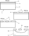
- the figure 1a is a schematic sectional side view of a structure 1 made in the first phase of a method of manufacturing a device according to a first embodiment of the invention.
- This structure 1 comprises a top layer 2 of silicon oxide, very thin, for example from a few nanometers to 100 nm, which covers a layer 3 in germanium, with a thickness of the order of 100 nm to a few microns. It then comprises a layer 4 of silicon oxide, with a thickness of the order of 1 micron. The whole is arranged on a silicon substrate.
- the figure 1b represents the result obtained after a first step of lithographing drawings on the first upper layer 2 using for example a negative resin, before etching the silicon oxide for example by argon etching. This results in an upper layer 2 forming a hard mask, comprising openings 2 'through.
- the figure 1c represents the structure after a step of etching germanium, carried out for example by a technique known by its acronym RIE, for the English terminology of Reactive Ion Etching.
- This etching step reproduces in the layer 3 of germanium the drawings formed in the upper layer 2, to form 3 'through openings in the germanium layer superimposed on the openings 2' of the upper layer 2.
- the figure 1d represents the final structure obtained after an etching of the silicon oxide layer 4 placed under the germanium, for example by HF etching in the vapor or liquid phase until the membrane is released, that is to say that the etching is stopped when it reaches laterally the base of the traction arms.
- the layer 4 of silicon oxide thus serves here as a sacrificial layer, and following removal by etching, the germanium membrane 20 is found automatically energized, by the intrinsic properties of the resulting structure.
- the figure 2a is a schematic side sectional view of a structure 11 made in the first phase of a method of manufacturing a device according to a second embodiment of the invention.
- This structure 11 likewise comprises an upper layer 12 of silicon oxide, which covers a layer 13 of Germanium, itself directly epitaxial on a silicon substrate 15.
- the figure 2b represents the result obtained after a first step similar to the step described in the first embodiment, of lithographing drawings on the first upper etching layer 12 of the silicon oxide to form an upper layer 12 comprising openings 12 through to form a mask for the next stage of germanium etching.
- the Figure 2c thus represents the resulting structure after this step of etching germanium, which reproduces in the germanium layer 13 the drawings of the upper layer 12, forming apertures 13 'through the germanium layer, superimposed on the openings 12' of the layer superior 12.
- the figure 2d represents the final structure obtained after an etching of the silicon layer 15 to form a cavity 44 disposed under germanium, for example by wet etching with tetramethylammonium hydroxide (TMAH), which selectively etches silicon with respect to germanium at a sufficient depth to release the membrane.
- TMAH tetramethylammonium hydroxide
- the silicon layer 15 therefore fulfills the function of sacrificial layer. This results in a suspended germanium membrane.
- the methods used are advantageously similar and compatible with the CMOS processes used for the manufacture of silicon-based electronic components.
- the etchings made in the preceding steps of the manufacturing processes, forming openings 2 ', 3', 12 ', 13' to finally obtain a suspended germanium membrane 20, have a particular shape advantageous.
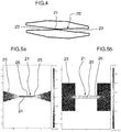
- the Figures 3a to 3d are exemplary embodiments of germanium membranes according to different embodiments of the invention. In fact, these figures show, in plan views, structures such as represented in side section by the figures 1d and 2d .
- Each membrane 20 is broken down into a central part, called the active zone 21 or zone of interest, where the voltage is concentrated, which makes it possible to provide the active zone 21 with interesting optical, electronic and structural properties under the effect of traction arms. 23, connecting the active area 21 to the rest of the structure.
- the active zone 21 is in the form of a regular polygon, rotationally symmetrical.
- this polygon comprises respectively 4 (particular case of the square), 6, 8 and 12 sides.
- this polygon could be irregular, while keeping a symmetry of rotation, for example of rectangle shape, truncated rectangle, ...
- the traction arms 23 are connected to one side 24 on two 24, 22 of the polygon forming the active zone 21.
- any combination of a number of traction arms 23 associated with a zone active comprising a number of multiple sides of the number of traction arms could be envisaged, distributing favorably the traction arms in a regular manner, and symmetrical around the active area.
- the traction arms 23 advantageously have trapezoidal shapes, comprising on the one hand a small side 24 at the boundary with the active zone 21, by definition parallel to one side of the active zone 21, and a larger side 34 to opposite, parallel to the short side 24, connected by two lateral sides 32.
- Each traction arm 23 advantageously comprises a shape whose width increases away from the active zone 21.
- Each lateral side 32 of a traction arm 23 forms an obtuse angle ⁇ with the side 24 of the active zone 21 with which it is connected, thus greater than 90 degrees.
- the lateral side 32 is beyond the perpendicular P to the side 24 of the active zone 21, giving a flared shape to the traction arm 23.
- the two lateral sides 32 of a traction arm 23 are not parallel to each other . They preferably move away symmetrically with respect to the side 24 of the active zone 21, to exert homogeneous stresses on the active zone 21.
- Figures 3a to 3d are intentionally schematic and perfect. In reality, the forms obtained will be less regular, less perfect, but will approach these forms.
- the figure 4 shows the shape obtained according to a real example of manufacturing a membrane 20 with two traction arms 23, approaching the shape of the figure 3a .
- the Figures 5a and 5b represent deformation levels obtained using a calculator on two exemplary membranes.
- the active zone 21 has a width of 1 micron for a length of 8 microns, and the traction arms 23 have a length of 28 microns.
- the deformations (and therefore the stresses) obtained within the membrane have a good uniformity, more precisely a ratio between the maximum deformation observed in the corners of the active zone at the border 24 with the traction arms 23 and the deformation at the center 26 of the order of 1.45.
- the comparative example simulated with two rectangular pulling arms 23, represented by the figure 5b the same ratio is 2.57.
- the figure 6 also illustrates the uniformity of the distribution of the deformations within a membrane with three traction arms 23, of trapezoidal shape, in a realization close to the geometry of the figure 3b .
- the periphery of the active zone 21 comprises rounded connections between the adjacent traction arms 23, forming a concave active zone 21.
- This approach removes the angles, which reduces still areas of strong constraints.
- polygonal shape of the active zone 21 of the membrane 20 according to the invention we also mean a shape with curved sides 22 '.
- Embodiments of the invention have been previously illustrated by way of non-limiting examples. Naturally, other forms of membranes may be chosen while remaining within the scope of the invention.
- all the traction arms may not be identical, although it is advantageous to use arms of the same shape, uniformly distributed around the active area, to find the most homogeneous geometry possible. It is generally also preferable to use at least three traction arms.
- the invention is implemented when at least three traction arms 23 each have a width that increases away from the active area, at least a portion of the length of each arm.
- traction arms connected to an active zone have been shown at a width corresponding to a side 24 of a polygon of the active zone.
- the active zone may have other shapes and the connection between a traction arm 23 and the active zone 21 may differ from the width of a side 24 of a polygon.
- a germanium-based alloy such as SiGe, SiGeSn, or layer stackings. different materials based on germanium.
- Such a germanium membrane according to the invention allows the realization of several types of optical and / or electronic devices.
- a diode a transistor, a luminescent device such as a laser, a photodetector.
- the stressed material is the active material for the intended application.
- this stressed material can also be used as a new substrate material to achieve the growth of another material which will then be the active material for the intended application.
- the quality of the crystalline growth of a thin-film material on a substrate is highly dependent on the difference between the mesh parameters of the substrate and the layer: these two parameters must be as close as possible to avoid growth defects.
- this problem is solved for example by depositing a buffer intermediate layer before the growth of the active material to adapt the mesh parameters but this imposes additional steps during manufacture.
- the invention it is then possible to produce a substrate on demand, whose mesh parameter will be adjusted to that of the active material: it suffices to apply the constraints necessary to stretch the crystalline structure of the substrate until a mesh as close as possible to that of the growth material, then to achieve growth. These variations can be significant up to a few percent.
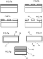
- FIGS. 7a to 7g represent different steps of a method of manufacturing a laser incorporating germanium membranes according to an embodiment of the invention, more specifically a cavity-emitting vertical cavity laser (VCSEL).
- VCSEL cavity-emitting vertical cavity laser
- the first stages of manufacture correspond to the steps described above with reference to the Figures 1a to 1d to obtain a germanium membrane.
- the shape of the membranes 20 is chosen to achieve a sufficient deformation in the active zone greater than 1.6%, to obtain the laser effect using germanium.
- the shape of the membrane 20 according to the figures 3b and 6 is good for example.
- the process then comprises a further step of deposition of aluminum on the germanium membrane as represented by figure 7e .
- An additional step removes the aluminum above and on the sides of the membrane 20, leaving only the aluminum layer under the membrane, as shown by FIG. figure 7f .
- an argon beam etching can be implemented, having taken care to have a layer of alumina 42 under the aluminum to form a stop layer during this etching.
- the aluminum thus forms a first mirror 41.
- a second conventional mirror 43 for example a dielectric mirror, in particular a Bragg mirror.
- a second conventional mirror 43 for example a dielectric mirror, in particular a Bragg mirror.
- an evaporator deposition of weak layers and high indices can be implemented, to obtain the membrane 20 illustrated by the figure 7g , comprising two lower and upper mirrors. These layers are designed so as to induce little stress and do not affect the deformation of the membrane 20 in the active zone.
- the figure 8 illustrates the sectional structure of the laser obtained, comprising a cavity 44 comprising both types of mirrors 41, 43.
- the membrane active zone and / or arm
- the membrane can be structured to dimensions between ⁇ / 10 and 10 ⁇ to form a photonic crystal.
Landscapes
- Physics & Mathematics (AREA)
- Engineering & Computer Science (AREA)
- Condensed Matter Physics & Semiconductors (AREA)
- General Physics & Mathematics (AREA)
- Electromagnetism (AREA)
- Optics & Photonics (AREA)
- Mechanical Engineering (AREA)
- Computer Hardware Design (AREA)
- Microelectronics & Electronic Packaging (AREA)
- Semiconductor Lasers (AREA)
- Weting (AREA)
- Recrystallisation Techniques (AREA)
- Light Receiving Elements (AREA)
Claims (10)
- Optische und/oder elektronische Vorrichtung, welche eine aufgehängte Membran (20) auf der Basis von Germanium umfasst, die einen aktiven Bereich (21) umfasst, der von Zugarmen (23) gespannt wird, dadurch gekennzeichnet, dass sie wenigstens drei Zugarme (23) umfasst, die nicht parallele laterale Seiten (32) umfassen, deren Breite mit zunehmendem Abstand vom aktiven Bereich (21) zunimmt und deren laterale Seiten (32) an der Grenze zwischen dem Zugarm (23) und dem aktiven Bereich (21) einen stumpfen Winkel mit dem aktiven Bereich (21) bilden.
- Optische und/oder elektronische Vorrichtung nach dem vorhergehenden Anspruch, dadurch gekennzeichnet, dass sie wenigstens einen Zugarm (23) von trapezförmiger Gestalt umfasst.
- Optische und/oder elektronische Vorrichtung nach einem der vorhergehenden Ansprüche, dadurch gekennzeichnet, dass alle Zugarme (23) dieselbe Form aufweisen und regelmäßig um den aktiven Bereich (21) herum verteilt sind.
- Optische und/oder elektronische Vorrichtung nach einem der vorhergehenden Ansprüche, dadurch gekennzeichnet, dass sie einen im Wesentlichen polygonalen aktiven Bereich (21), der insbesondere ein regelmäßiges Vieleck bildet, umfasst, dessen Anzahl der Seiten (22, 24) ein Vielfaches der Anzahl der Zugarme (23) ist.
- Optische und/oder elektronische Vorrichtung nach einem der vorhergehenden Ansprüche, dadurch gekennzeichnet, dass sie am Umfang des aktiven Bereichs (21) abgerundete Verbindungen (22') umfasst, welche zwei Zugarme (23) verbinden.
- Optische und/oder elektronische Vorrichtung nach einem der vorhergehenden Ansprüche, dadurch gekennzeichnet, dass sie eine Diode, ein Transistor, eine Lumineszenzvorrichtung, ein Laser, ein Fotodetektor, ein Substrat ist.
- Optische und/oder elektronische Vorrichtung nach dem vorhergehenden Anspruch, dadurch gekennzeichnet, dass sie eine optische Vorrichtung ist, und dadurch, dass sie einen ersten Spiegel (41) unter der Membran (20) auf der Basis von Germanium und/oder einen zweiten Spiegel (43) darüber umfasst.
- Verfahren zur Herstellung einer optischen und/oder elektronischen Vorrichtung, dadurch gekennzeichnet, dass es die folgenden Schritte umfasst:- Ätzen einer Schicht (3; 13) auf der Basis von Germanium, um wenigstens drei Zugarme (23) zu bilden, die nicht parallele laterale Seiten (32) umfassen, deren Breite mit zunehmendem Abstand von einem aktiven Bereich (21) zunimmt und deren laterale Seiten (32) an der Grenze zwischen dem Zugarm (23) und dem aktiven Bereich (21) einen stumpfen Winkel mit dem aktiven Bereich (21) bilden;- Ätzen einer Opferschicht (4; 15) unter der Schicht (3; 13) auf der Basis von Germanium, um eine aufgehängte Membran (20) auf der Basis von Germanium zu erhalten, die den aktiven Bereich (21) und den wenigstens einen Zugarm (23) umfasst.
- Verfahren zur Herstellung einer optischen und/oder elektronischen Vorrichtung nach dem vorhergehenden Anspruch, dadurch gekennzeichnet, dass der Schritt des Ätzens der Opferschicht fortschreitend vom Mittelpunkt der Membran (20) am aktiven Bereich (21) bis zum äußeren Rand der Zugarme (23) ausgeführt wird.
- Verfahren zur Herstellung einer optischen und/oder elektronischen Vorrichtung nach Anspruch 8 oder 9, dadurch gekennzeichnet, dass es einen Schritt der Aufbringung einer reflektierenden Schicht, um einen Spiegel (41), insbesondere aus Aluminium, unter der Membran (20) auszubilden, und/oder einen zweiten Schritt der Aufbringung einer reflektierenden Schicht, um einen Spiegel auf der Membran auszubilden, umfasst.
Applications Claiming Priority (1)
| Application Number | Priority Date | Filing Date | Title |
|---|---|---|---|
| FR1455805A FR3022684B1 (fr) | 2014-06-23 | 2014-06-23 | Dispositif a membrane a germanium sous contrainte |
Publications (2)
| Publication Number | Publication Date |
|---|---|
| EP2960203A1 EP2960203A1 (de) | 2015-12-30 |
| EP2960203B1 true EP2960203B1 (de) | 2019-11-06 |
Family
ID=51862404
Family Applications (1)
| Application Number | Title | Priority Date | Filing Date |
|---|---|---|---|
| EP15171976.2A Active EP2960203B1 (de) | 2014-06-23 | 2015-06-12 | Vorrichtung mit einer membran auf der basis von unter zugbelastung stehendem germanium |
Country Status (4)
| Country | Link |
|---|---|
| US (1) | US9502864B2 (de) |
| EP (1) | EP2960203B1 (de) |
| JP (1) | JP6664892B2 (de) |
| FR (1) | FR3022684B1 (de) |
Families Citing this family (8)
| Publication number | Priority date | Publication date | Assignee | Title |
|---|---|---|---|---|
| WO2016120214A1 (en) | 2015-01-26 | 2016-08-04 | Cirrus Logic International Semiconductor Limited | Mems devices and processes |
| KR102181323B1 (ko) * | 2016-04-06 | 2020-11-23 | 한국전자통신연구원 | 레이저 장치 및 이의 제조방법 |
| FR3055467B1 (fr) | 2016-08-26 | 2018-09-21 | Commissariat A L'energie Atomique Et Aux Energies Alternatives | Procede de realisation d’une couche contrainte en tension a base de germanium etain |
| FR3069859B1 (fr) * | 2017-08-03 | 2019-08-23 | Commissariat A L'energie Atomique Et Aux Energies Alternatives | Structure semiconductrice comportant une membrane suspendue a portion centrale structuree en epaisseur |
| FR3095893A1 (fr) | 2019-05-09 | 2020-11-13 | Commissariat A L'energie Atomique Et Aux Energies Alternatives | dispositif optoélectronique comportant une portion centrale contrainte en tension suivant un premier axe et polarisee électriquement suivant un deuxième axe |
| WO2020245866A1 (ja) * | 2019-06-03 | 2020-12-10 | 日本電信電話株式会社 | 光デバイス |
| GB2626454B (en) * | 2019-10-23 | 2024-10-16 | Smart Photonics Holding B V | Manufacturing a semiconductor structure |
| GB2588891B (en) | 2019-10-23 | 2024-04-24 | Smart Photonics Holding B V | Manufacturing a semiconductor structure |
Family Cites Families (4)
| Publication number | Priority date | Publication date | Assignee | Title |
|---|---|---|---|---|
| JP2617287B2 (ja) * | 1995-09-06 | 1997-06-04 | シャープ株式会社 | シリコンマイクロセンサ |
| GB2501307A (en) * | 2012-04-19 | 2013-10-23 | Univ Warwick | Suspended Ge or Si-Ge semiconductor structure on mono-crystal line Si substrate |
| CA2879749C (en) * | 2012-07-27 | 2020-12-08 | Thorlabs,Inc. | Polarization stable widely tunable short cavity laser |
| KR101946035B1 (ko) * | 2012-09-18 | 2019-04-25 | 한국전자통신연구원 | 수직공진 표면방출 레이저 및 그의 제조방법 |
-
2014
- 2014-06-23 FR FR1455805A patent/FR3022684B1/fr not_active Expired - Fee Related
-
2015
- 2015-06-12 EP EP15171976.2A patent/EP2960203B1/de active Active
- 2015-06-18 US US14/742,971 patent/US9502864B2/en not_active Expired - Fee Related
- 2015-06-22 JP JP2015124423A patent/JP6664892B2/ja not_active Expired - Fee Related
Non-Patent Citations (1)
| Title |
|---|
| None * |
Also Published As
| Publication number | Publication date |
|---|---|
| FR3022684A1 (fr) | 2015-12-25 |
| JP2016021565A (ja) | 2016-02-04 |
| JP6664892B2 (ja) | 2020-03-13 |
| US20150372454A1 (en) | 2015-12-24 |
| EP2960203A1 (de) | 2015-12-30 |
| US9502864B2 (en) | 2016-11-22 |
| FR3022684B1 (fr) | 2017-10-27 |
Similar Documents
| Publication | Publication Date | Title |
|---|---|---|
| EP2960203B1 (de) | Vorrichtung mit einer membran auf der basis von unter zugbelastung stehendem germanium | |
| EP3563420B1 (de) | Verfahren zur herstellung einer optoelektronischen vorrichtung mit fotolumineszenten pads aus fotolack | |
| EP2973750B1 (de) | Verfahren zur herstellung von leuchtdioden | |
| EP3151265B1 (de) | Herstellungsverfahren einer halbleiterstruktur, die einen spannabschnitt umfasst | |
| FR2896913A1 (fr) | Procede de fabrication d'une tranche de quasi-substrat et corps semi-conducteur produit en utilisant une tranche de quasi-substrat de ce genre | |
| EP3987574B1 (de) | Verfahren zur herstellung von nitrid-kacheln zur herstellung einer elektronischen oder optoelektronischen vorrichtung | |
| EP4128324A1 (de) | Entfernbare struktur zur übertragung oder manipulation von schichten und verfahren zur übertragung einer schicht mit dieser abnehmbaren struktur | |
| EP3384521B1 (de) | Verfahren zur herstellung einer halbpolaren nitridschicht auf einem kristallinen substrat | |
| EP3151266B1 (de) | Verfahren zur erstellung eines halbleiterabschnitts durch epitaxisches wachstum auf einem verspannten abschnitt | |
| EP2191306B1 (de) | Dispersive optische vorrichtung mit dreidimensionalem photonenkristall | |
| EP3764409B1 (de) | Quelle einzelner photonen mit einem hohen ununterscheidbarkeitsfaktor | |
| FR2933502A1 (fr) | Structure de guide d'onde optique micronanostructure pour le controle de la birefringence | |
| EP3348518A1 (de) | Quelle für kollimiertes licht, ihr herstellungsverfahren und ihre verwendung für die emission von einzelnen photonen | |
| EP2697825B1 (de) | Verfahren zur herstellung einer optoelektrischen vorrichtung | |
| EP3438041B1 (de) | Halbleiterstruktur die eine aufgespannte membran mit einem in der dicke strukturierten zentralen abschnitt umfasst | |
| EP4009456B1 (de) | Verfahren zur herstellung eines verteilten bragg-spiegels | |
| EP2383775B1 (de) | Method for obtaining a layer of AlN with substantially vertical flanks | |
| EP4020525A1 (de) | Verfahren zur herstellung einer nitridschicht | |
| EP4539101A1 (de) | Verfahren zur herstellung einer zusammenhängenden nitridschicht | |
| EP3772145A1 (de) | Hybride laserquelle, die einen integrierten wellenleiter mit einem zwischengeschalteten bragg-gitter umfasst | |
| EP2232314B1 (de) | Verfahren zur herstellung eines strukturierten materials mit durchgangsöffnungen, im besonderen nach photonenkristallstrukturen strukturierte nitride der typ-iii-halbleiter | |
| EP4205177B1 (de) | Verfahren zur herstellung einer optoelektronischen vorrichtung | |
| WO2005012160A2 (fr) | Procede de desolidarisation d’une couche utile et composant obtenu par ce procede | |
| EP4446102A1 (de) | Verfahren zur herstellung einer dreidimensionalen biegestruktur | |
| EP4634988A1 (de) | Verfahren zur vorbereitung eines stapels zum bonden |
Legal Events
| Date | Code | Title | Description |
|---|---|---|---|
| PUAI | Public reference made under article 153(3) epc to a published international application that has entered the european phase |
Free format text: ORIGINAL CODE: 0009012 |
|
| AK | Designated contracting states |
Kind code of ref document: A1 Designated state(s): AL AT BE BG CH CY CZ DE DK EE ES FI FR GB GR HR HU IE IS IT LI LT LU LV MC MK MT NL NO PL PT RO RS SE SI SK SM TR |
|
| AX | Request for extension of the european patent |
Extension state: BA ME |
|
| 17P | Request for examination filed |
Effective date: 20160617 |
|
| RBV | Designated contracting states (corrected) |
Designated state(s): AL AT BE BG CH CY CZ DE DK EE ES FI FR GB GR HR HU IE IS IT LI LT LU LV MC MK MT NL NO PL PT RO RS SE SI SK SM TR |
|
| GRAP | Despatch of communication of intention to grant a patent |
Free format text: ORIGINAL CODE: EPIDOSNIGR1 |
|
| STAA | Information on the status of an ep patent application or granted ep patent |
Free format text: STATUS: GRANT OF PATENT IS INTENDED |
|
| RIC1 | Information provided on ipc code assigned before grant |
Ipc: B81B 3/00 20060101AFI20181002BHEP |
|
| INTG | Intention to grant announced |
Effective date: 20181105 |
|
| RIN1 | Information on inventor provided before grant (corrected) |
Inventor name: GUILLOY, KEVIN Inventor name: REBOUD, VINCENT Inventor name: PAUC, NICOLAS Inventor name: CALVO, VINCENT |
|
| GRAJ | Information related to disapproval of communication of intention to grant by the applicant or resumption of examination proceedings by the epo deleted |
Free format text: ORIGINAL CODE: EPIDOSDIGR1 |
|
| STAA | Information on the status of an ep patent application or granted ep patent |
Free format text: STATUS: REQUEST FOR EXAMINATION WAS MADE |
|
| INTC | Intention to grant announced (deleted) | ||
| GRAS | Grant fee paid |
Free format text: ORIGINAL CODE: EPIDOSNIGR3 |
|
| STAA | Information on the status of an ep patent application or granted ep patent |
Free format text: STATUS: GRANT OF PATENT IS INTENDED |
|
| GRAP | Despatch of communication of intention to grant a patent |
Free format text: ORIGINAL CODE: EPIDOSNIGR1 |
|
| INTG | Intention to grant announced |
Effective date: 20190604 |
|
| GRAA | (expected) grant |
Free format text: ORIGINAL CODE: 0009210 |
|
| STAA | Information on the status of an ep patent application or granted ep patent |
Free format text: STATUS: THE PATENT HAS BEEN GRANTED |
|
| AK | Designated contracting states |
Kind code of ref document: B1 Designated state(s): AL AT BE BG CH CY CZ DE DK EE ES FI FR GB GR HR HU IE IS IT LI LT LU LV MC MK MT NL NO PL PT RO RS SE SI SK SM TR |
|
| REG | Reference to a national code |
Ref country code: GB Ref legal event code: FG4D Free format text: NOT ENGLISH |
|
| REG | Reference to a national code |
Ref country code: CH Ref legal event code: EP Ref country code: AT Ref legal event code: REF Ref document number: 1198499 Country of ref document: AT Kind code of ref document: T Effective date: 20191115 |
|
| REG | Reference to a national code |
Ref country code: IE Ref legal event code: FG4D Free format text: LANGUAGE OF EP DOCUMENT: FRENCH |
|
| REG | Reference to a national code |
Ref country code: DE Ref legal event code: R096 Ref document number: 602015040964 Country of ref document: DE |
|
| REG | Reference to a national code |
Ref country code: NL Ref legal event code: MP Effective date: 20191106 |
|
| REG | Reference to a national code |
Ref country code: LT Ref legal event code: MG4D |
|
| PG25 | Lapsed in a contracting state [announced via postgrant information from national office to epo] |
Ref country code: SE Free format text: LAPSE BECAUSE OF FAILURE TO SUBMIT A TRANSLATION OF THE DESCRIPTION OR TO PAY THE FEE WITHIN THE PRESCRIBED TIME-LIMIT Effective date: 20191106 Ref country code: LV Free format text: LAPSE BECAUSE OF FAILURE TO SUBMIT A TRANSLATION OF THE DESCRIPTION OR TO PAY THE FEE WITHIN THE PRESCRIBED TIME-LIMIT Effective date: 20191106 Ref country code: LT Free format text: LAPSE BECAUSE OF FAILURE TO SUBMIT A TRANSLATION OF THE DESCRIPTION OR TO PAY THE FEE WITHIN THE PRESCRIBED TIME-LIMIT Effective date: 20191106 Ref country code: NL Free format text: LAPSE BECAUSE OF FAILURE TO SUBMIT A TRANSLATION OF THE DESCRIPTION OR TO PAY THE FEE WITHIN THE PRESCRIBED TIME-LIMIT Effective date: 20191106 Ref country code: FI Free format text: LAPSE BECAUSE OF FAILURE TO SUBMIT A TRANSLATION OF THE DESCRIPTION OR TO PAY THE FEE WITHIN THE PRESCRIBED TIME-LIMIT Effective date: 20191106 Ref country code: BG Free format text: LAPSE BECAUSE OF FAILURE TO SUBMIT A TRANSLATION OF THE DESCRIPTION OR TO PAY THE FEE WITHIN THE PRESCRIBED TIME-LIMIT Effective date: 20200206 Ref country code: GR Free format text: LAPSE BECAUSE OF FAILURE TO SUBMIT A TRANSLATION OF THE DESCRIPTION OR TO PAY THE FEE WITHIN THE PRESCRIBED TIME-LIMIT Effective date: 20200207 Ref country code: PT Free format text: LAPSE BECAUSE OF FAILURE TO SUBMIT A TRANSLATION OF THE DESCRIPTION OR TO PAY THE FEE WITHIN THE PRESCRIBED TIME-LIMIT Effective date: 20200306 Ref country code: PL Free format text: LAPSE BECAUSE OF FAILURE TO SUBMIT A TRANSLATION OF THE DESCRIPTION OR TO PAY THE FEE WITHIN THE PRESCRIBED TIME-LIMIT Effective date: 20191106 Ref country code: NO Free format text: LAPSE BECAUSE OF FAILURE TO SUBMIT A TRANSLATION OF THE DESCRIPTION OR TO PAY THE FEE WITHIN THE PRESCRIBED TIME-LIMIT Effective date: 20200206 |
|
| PG25 | Lapsed in a contracting state [announced via postgrant information from national office to epo] |
Ref country code: RS Free format text: LAPSE BECAUSE OF FAILURE TO SUBMIT A TRANSLATION OF THE DESCRIPTION OR TO PAY THE FEE WITHIN THE PRESCRIBED TIME-LIMIT Effective date: 20191106 Ref country code: HR Free format text: LAPSE BECAUSE OF FAILURE TO SUBMIT A TRANSLATION OF THE DESCRIPTION OR TO PAY THE FEE WITHIN THE PRESCRIBED TIME-LIMIT Effective date: 20191106 Ref country code: IS Free format text: LAPSE BECAUSE OF FAILURE TO SUBMIT A TRANSLATION OF THE DESCRIPTION OR TO PAY THE FEE WITHIN THE PRESCRIBED TIME-LIMIT Effective date: 20200306 |
|
| PG25 | Lapsed in a contracting state [announced via postgrant information from national office to epo] |
Ref country code: AL Free format text: LAPSE BECAUSE OF FAILURE TO SUBMIT A TRANSLATION OF THE DESCRIPTION OR TO PAY THE FEE WITHIN THE PRESCRIBED TIME-LIMIT Effective date: 20191106 |
|
| PG25 | Lapsed in a contracting state [announced via postgrant information from national office to epo] |
Ref country code: CZ Free format text: LAPSE BECAUSE OF FAILURE TO SUBMIT A TRANSLATION OF THE DESCRIPTION OR TO PAY THE FEE WITHIN THE PRESCRIBED TIME-LIMIT Effective date: 20191106 Ref country code: RO Free format text: LAPSE BECAUSE OF FAILURE TO SUBMIT A TRANSLATION OF THE DESCRIPTION OR TO PAY THE FEE WITHIN THE PRESCRIBED TIME-LIMIT Effective date: 20191106 Ref country code: ES Free format text: LAPSE BECAUSE OF FAILURE TO SUBMIT A TRANSLATION OF THE DESCRIPTION OR TO PAY THE FEE WITHIN THE PRESCRIBED TIME-LIMIT Effective date: 20191106 Ref country code: DK Free format text: LAPSE BECAUSE OF FAILURE TO SUBMIT A TRANSLATION OF THE DESCRIPTION OR TO PAY THE FEE WITHIN THE PRESCRIBED TIME-LIMIT Effective date: 20191106 Ref country code: EE Free format text: LAPSE BECAUSE OF FAILURE TO SUBMIT A TRANSLATION OF THE DESCRIPTION OR TO PAY THE FEE WITHIN THE PRESCRIBED TIME-LIMIT Effective date: 20191106 |
|
| REG | Reference to a national code |
Ref country code: DE Ref legal event code: R097 Ref document number: 602015040964 Country of ref document: DE |
|
| REG | Reference to a national code |
Ref country code: AT Ref legal event code: MK05 Ref document number: 1198499 Country of ref document: AT Kind code of ref document: T Effective date: 20191106 |
|
| PG25 | Lapsed in a contracting state [announced via postgrant information from national office to epo] |
Ref country code: SK Free format text: LAPSE BECAUSE OF FAILURE TO SUBMIT A TRANSLATION OF THE DESCRIPTION OR TO PAY THE FEE WITHIN THE PRESCRIBED TIME-LIMIT Effective date: 20191106 Ref country code: SM Free format text: LAPSE BECAUSE OF FAILURE TO SUBMIT A TRANSLATION OF THE DESCRIPTION OR TO PAY THE FEE WITHIN THE PRESCRIBED TIME-LIMIT Effective date: 20191106 |
|
| PLBE | No opposition filed within time limit |
Free format text: ORIGINAL CODE: 0009261 |
|
| STAA | Information on the status of an ep patent application or granted ep patent |
Free format text: STATUS: NO OPPOSITION FILED WITHIN TIME LIMIT |
|
| 26N | No opposition filed |
Effective date: 20200807 |
|
| PG25 | Lapsed in a contracting state [announced via postgrant information from national office to epo] |
Ref country code: AT Free format text: LAPSE BECAUSE OF FAILURE TO SUBMIT A TRANSLATION OF THE DESCRIPTION OR TO PAY THE FEE WITHIN THE PRESCRIBED TIME-LIMIT Effective date: 20191106 Ref country code: SI Free format text: LAPSE BECAUSE OF FAILURE TO SUBMIT A TRANSLATION OF THE DESCRIPTION OR TO PAY THE FEE WITHIN THE PRESCRIBED TIME-LIMIT Effective date: 20191106 |
|
| PG25 | Lapsed in a contracting state [announced via postgrant information from national office to epo] |
Ref country code: IT Free format text: LAPSE BECAUSE OF FAILURE TO SUBMIT A TRANSLATION OF THE DESCRIPTION OR TO PAY THE FEE WITHIN THE PRESCRIBED TIME-LIMIT Effective date: 20191106 Ref country code: MC Free format text: LAPSE BECAUSE OF FAILURE TO SUBMIT A TRANSLATION OF THE DESCRIPTION OR TO PAY THE FEE WITHIN THE PRESCRIBED TIME-LIMIT Effective date: 20191106 |
|
| REG | Reference to a national code |
Ref country code: CH Ref legal event code: PL |
|
| PG25 | Lapsed in a contracting state [announced via postgrant information from national office to epo] |
Ref country code: LU Free format text: LAPSE BECAUSE OF NON-PAYMENT OF DUE FEES Effective date: 20200612 |
|
| REG | Reference to a national code |
Ref country code: BE Ref legal event code: MM Effective date: 20200630 |
|
| PG25 | Lapsed in a contracting state [announced via postgrant information from national office to epo] |
Ref country code: LI Free format text: LAPSE BECAUSE OF NON-PAYMENT OF DUE FEES Effective date: 20200630 Ref country code: IE Free format text: LAPSE BECAUSE OF NON-PAYMENT OF DUE FEES Effective date: 20200612 Ref country code: CH Free format text: LAPSE BECAUSE OF NON-PAYMENT OF DUE FEES Effective date: 20200630 |
|
| PG25 | Lapsed in a contracting state [announced via postgrant information from national office to epo] |
Ref country code: BE Free format text: LAPSE BECAUSE OF NON-PAYMENT OF DUE FEES Effective date: 20200630 |
|
| PGFP | Annual fee paid to national office [announced via postgrant information from national office to epo] |
Ref country code: DE Payment date: 20210616 Year of fee payment: 7 Ref country code: FR Payment date: 20210630 Year of fee payment: 7 |
|
| PGFP | Annual fee paid to national office [announced via postgrant information from national office to epo] |
Ref country code: GB Payment date: 20210622 Year of fee payment: 7 |
|
| PG25 | Lapsed in a contracting state [announced via postgrant information from national office to epo] |
Ref country code: TR Free format text: LAPSE BECAUSE OF FAILURE TO SUBMIT A TRANSLATION OF THE DESCRIPTION OR TO PAY THE FEE WITHIN THE PRESCRIBED TIME-LIMIT Effective date: 20191106 Ref country code: MT Free format text: LAPSE BECAUSE OF FAILURE TO SUBMIT A TRANSLATION OF THE DESCRIPTION OR TO PAY THE FEE WITHIN THE PRESCRIBED TIME-LIMIT Effective date: 20191106 Ref country code: CY Free format text: LAPSE BECAUSE OF FAILURE TO SUBMIT A TRANSLATION OF THE DESCRIPTION OR TO PAY THE FEE WITHIN THE PRESCRIBED TIME-LIMIT Effective date: 20191106 |
|
| PG25 | Lapsed in a contracting state [announced via postgrant information from national office to epo] |
Ref country code: MK Free format text: LAPSE BECAUSE OF FAILURE TO SUBMIT A TRANSLATION OF THE DESCRIPTION OR TO PAY THE FEE WITHIN THE PRESCRIBED TIME-LIMIT Effective date: 20191106 |
|
| REG | Reference to a national code |
Ref country code: DE Ref legal event code: R119 Ref document number: 602015040964 Country of ref document: DE |
|
| GBPC | Gb: european patent ceased through non-payment of renewal fee |
Effective date: 20220612 |
|
| PG25 | Lapsed in a contracting state [announced via postgrant information from national office to epo] |
Ref country code: FR Free format text: LAPSE BECAUSE OF NON-PAYMENT OF DUE FEES Effective date: 20220630 |
|
| PG25 | Lapsed in a contracting state [announced via postgrant information from national office to epo] |
Ref country code: GB Free format text: LAPSE BECAUSE OF NON-PAYMENT OF DUE FEES Effective date: 20220612 Ref country code: DE Free format text: LAPSE BECAUSE OF NON-PAYMENT OF DUE FEES Effective date: 20230103 |