EP2960489B1 - Appareil de contrôle - Google Patents
Appareil de contrôle Download PDFInfo
- Publication number
- EP2960489B1 EP2960489B1 EP15163085.2A EP15163085A EP2960489B1 EP 2960489 B1 EP2960489 B1 EP 2960489B1 EP 15163085 A EP15163085 A EP 15163085A EP 2960489 B1 EP2960489 B1 EP 2960489B1
- Authority
- EP
- European Patent Office
- Prior art keywords
- switch
- ics
- overheat prevention
- prevention component
- control apparatus
- Prior art date
- Legal status (The legal status is an assumption and is not a legal conclusion. Google has not performed a legal analysis and makes no representation as to the accuracy of the status listed.)
- Not-in-force
Links
- 230000002265 prevention Effects 0.000 claims description 54
- 239000004065 semiconductor Substances 0.000 claims description 18
- 230000031070 response to heat Effects 0.000 claims description 4
- 238000013021 overheating Methods 0.000 description 20
- 238000010586 diagram Methods 0.000 description 7
- 239000013256 coordination polymer Substances 0.000 description 6
- 230000008859 change Effects 0.000 description 5
- 230000000694 effects Effects 0.000 description 5
- 238000000034 method Methods 0.000 description 3
- 238000007796 conventional method Methods 0.000 description 2
- 230000003247 decreasing effect Effects 0.000 description 2
- 230000004927 fusion Effects 0.000 description 2
- 239000000155 melt Substances 0.000 description 2
- 230000004048 modification Effects 0.000 description 2
- 238000012986 modification Methods 0.000 description 2
- 229910000679 solder Inorganic materials 0.000 description 2
- 230000015572 biosynthetic process Effects 0.000 description 1
- 239000004020 conductor Substances 0.000 description 1
- 230000007423 decrease Effects 0.000 description 1
- WABPQHHGFIMREM-UHFFFAOYSA-N lead(0) Chemical compound [Pb] WABPQHHGFIMREM-UHFFFAOYSA-N 0.000 description 1
- 230000007257 malfunction Effects 0.000 description 1
- 238000004519 manufacturing process Methods 0.000 description 1
- 238000005476 soldering Methods 0.000 description 1
Images






Classifications
-
- H—ELECTRICITY
- H05—ELECTRIC TECHNIQUES NOT OTHERWISE PROVIDED FOR
- H05K—PRINTED CIRCUITS; CASINGS OR CONSTRUCTIONAL DETAILS OF ELECTRIC APPARATUS; MANUFACTURE OF ASSEMBLAGES OF ELECTRICAL COMPONENTS
- H05K1/00—Printed circuits
- H05K1/02—Details
- H05K1/0201—Thermal arrangements, e.g. for cooling, heating or preventing overheating
-
- F—MECHANICAL ENGINEERING; LIGHTING; HEATING; WEAPONS; BLASTING
- F02—COMBUSTION ENGINES; HOT-GAS OR COMBUSTION-PRODUCT ENGINE PLANTS
- F02P—IGNITION, OTHER THAN COMPRESSION IGNITION, FOR INTERNAL-COMBUSTION ENGINES; TESTING OF IGNITION TIMING IN COMPRESSION-IGNITION ENGINES
- F02P19/00—Incandescent ignition, e.g. during starting of internal combustion engines; Combination of incandescent and spark ignition
- F02P19/02—Incandescent ignition, e.g. during starting of internal combustion engines; Combination of incandescent and spark ignition electric, e.g. layout of circuits of apparatus having glowing plugs
- F02P19/027—Safety devices, e.g. for diagnosing the glow plugs or the related circuits
-
- H—ELECTRICITY
- H02—GENERATION; CONVERSION OR DISTRIBUTION OF ELECTRIC POWER
- H02H—EMERGENCY PROTECTIVE CIRCUIT ARRANGEMENTS
- H02H3/00—Emergency protective circuit arrangements for automatic disconnection directly responsive to an undesired change from normal electric working condition with or without subsequent reconnection ; integrated protection
- H02H3/08—Emergency protective circuit arrangements for automatic disconnection directly responsive to an undesired change from normal electric working condition with or without subsequent reconnection ; integrated protection responsive to excess current
- H02H3/085—Emergency protective circuit arrangements for automatic disconnection directly responsive to an undesired change from normal electric working condition with or without subsequent reconnection ; integrated protection responsive to excess current making use of a thermal sensor, e.g. thermistor, heated by the excess current
-
- H—ELECTRICITY
- H03—ELECTRONIC CIRCUITRY
- H03K—PULSE TECHNIQUE
- H03K17/00—Electronic switching or gating, i.e. not by contact-making and –breaking
- H03K17/08—Modifications for protecting switching circuit against overcurrent or overvoltage
- H03K17/081—Modifications for protecting switching circuit against overcurrent or overvoltage without feedback from the output circuit to the control circuit
- H03K17/0812—Modifications for protecting switching circuit against overcurrent or overvoltage without feedback from the output circuit to the control circuit by measures taken in the control circuit
- H03K17/08122—Modifications for protecting switching circuit against overcurrent or overvoltage without feedback from the output circuit to the control circuit by measures taken in the control circuit in field-effect transistor switches
-
- H—ELECTRICITY
- H05—ELECTRIC TECHNIQUES NOT OTHERWISE PROVIDED FOR
- H05K—PRINTED CIRCUITS; CASINGS OR CONSTRUCTIONAL DETAILS OF ELECTRIC APPARATUS; MANUFACTURE OF ASSEMBLAGES OF ELECTRICAL COMPONENTS
- H05K1/00—Printed circuits
- H05K1/18—Printed circuits structurally associated with non-printed electric components
- H05K1/181—Printed circuits structurally associated with non-printed electric components associated with surface mounted components
-
- H—ELECTRICITY
- H01—ELECTRIC ELEMENTS
- H01H—ELECTRIC SWITCHES; RELAYS; SELECTORS; EMERGENCY PROTECTIVE DEVICES
- H01H37/00—Thermally-actuated switches
- H01H37/02—Details
- H01H37/04—Bases; Housings; Mountings
- H01H2037/046—Bases; Housings; Mountings being soldered on the printed circuit to be protected
-
- H—ELECTRICITY
- H01—ELECTRIC ELEMENTS
- H01H—ELECTRIC SWITCHES; RELAYS; SELECTORS; EMERGENCY PROTECTIVE DEVICES
- H01H37/00—Thermally-actuated switches
- H01H37/74—Switches in which only the opening movement or only the closing movement of a contact is effected by heating or cooling
- H01H37/76—Contact member actuated by melting of fusible material, actuated due to burning of combustible material or due to explosion of explosive material
- H01H37/761—Contact member actuated by melting of fusible material, actuated due to burning of combustible material or due to explosion of explosive material with a fusible element forming part of the switched circuit
- H01H2037/762—Contact member actuated by melting of fusible material, actuated due to burning of combustible material or due to explosion of explosive material with a fusible element forming part of the switched circuit using a spring for opening the circuit when the fusible element melts
-
- H—ELECTRICITY
- H01—ELECTRIC ELEMENTS
- H01H—ELECTRIC SWITCHES; RELAYS; SELECTORS; EMERGENCY PROTECTIVE DEVICES
- H01H37/00—Thermally-actuated switches
- H01H37/74—Switches in which only the opening movement or only the closing movement of a contact is effected by heating or cooling
- H01H37/76—Contact member actuated by melting of fusible material, actuated due to burning of combustible material or due to explosion of explosive material
- H01H37/761—Contact member actuated by melting of fusible material, actuated due to burning of combustible material or due to explosion of explosive material with a fusible element forming part of the switched circuit
-
- H—ELECTRICITY
- H03—ELECTRONIC CIRCUITRY
- H03K—PULSE TECHNIQUE
- H03K17/00—Electronic switching or gating, i.e. not by contact-making and –breaking
- H03K17/08—Modifications for protecting switching circuit against overcurrent or overvoltage
- H03K2017/0806—Modifications for protecting switching circuit against overcurrent or overvoltage against excessive temperature
-
- H—ELECTRICITY
- H05—ELECTRIC TECHNIQUES NOT OTHERWISE PROVIDED FOR
- H05K—PRINTED CIRCUITS; CASINGS OR CONSTRUCTIONAL DETAILS OF ELECTRIC APPARATUS; MANUFACTURE OF ASSEMBLAGES OF ELECTRICAL COMPONENTS
- H05K2201/00—Indexing scheme relating to printed circuits covered by H05K1/00
- H05K2201/10—Details of components or other objects attached to or integrated in a printed circuit board
- H05K2201/10007—Types of components
- H05K2201/10022—Non-printed resistor
-
- H—ELECTRICITY
- H05—ELECTRIC TECHNIQUES NOT OTHERWISE PROVIDED FOR
- H05K—PRINTED CIRCUITS; CASINGS OR CONSTRUCTIONAL DETAILS OF ELECTRIC APPARATUS; MANUFACTURE OF ASSEMBLAGES OF ELECTRICAL COMPONENTS
- H05K2201/00—Indexing scheme relating to printed circuits covered by H05K1/00
- H05K2201/10—Details of components or other objects attached to or integrated in a printed circuit board
- H05K2201/10007—Types of components
- H05K2201/10053—Switch
-
- H—ELECTRICITY
- H05—ELECTRIC TECHNIQUES NOT OTHERWISE PROVIDED FOR
- H05K—PRINTED CIRCUITS; CASINGS OR CONSTRUCTIONAL DETAILS OF ELECTRIC APPARATUS; MANUFACTURE OF ASSEMBLAGES OF ELECTRICAL COMPONENTS
- H05K2201/00—Indexing scheme relating to printed circuits covered by H05K1/00
- H05K2201/10—Details of components or other objects attached to or integrated in a printed circuit board
- H05K2201/10007—Types of components
- H05K2201/10151—Sensor
-
- H—ELECTRICITY
- H05—ELECTRIC TECHNIQUES NOT OTHERWISE PROVIDED FOR
- H05K—PRINTED CIRCUITS; CASINGS OR CONSTRUCTIONAL DETAILS OF ELECTRIC APPARATUS; MANUFACTURE OF ASSEMBLAGES OF ELECTRICAL COMPONENTS
- H05K2201/00—Indexing scheme relating to printed circuits covered by H05K1/00
- H05K2201/10—Details of components or other objects attached to or integrated in a printed circuit board
- H05K2201/10007—Types of components
- H05K2201/10166—Transistor
-
- H—ELECTRICITY
- H05—ELECTRIC TECHNIQUES NOT OTHERWISE PROVIDED FOR
- H05K—PRINTED CIRCUITS; CASINGS OR CONSTRUCTIONAL DETAILS OF ELECTRIC APPARATUS; MANUFACTURE OF ASSEMBLAGES OF ELECTRICAL COMPONENTS
- H05K2201/00—Indexing scheme relating to printed circuits covered by H05K1/00
- H05K2201/10—Details of components or other objects attached to or integrated in a printed circuit board
- H05K2201/10007—Types of components
- H05K2201/10181—Fuse
-
- H—ELECTRICITY
- H05—ELECTRIC TECHNIQUES NOT OTHERWISE PROVIDED FOR
- H05K—PRINTED CIRCUITS; CASINGS OR CONSTRUCTIONAL DETAILS OF ELECTRIC APPARATUS; MANUFACTURE OF ASSEMBLAGES OF ELECTRICAL COMPONENTS
- H05K2201/00—Indexing scheme relating to printed circuits covered by H05K1/00
- H05K2201/10—Details of components or other objects attached to or integrated in a printed circuit board
- H05K2201/10431—Details of mounted components
- H05K2201/10507—Involving several components
- H05K2201/10515—Stacked components
-
- H—ELECTRICITY
- H05—ELECTRIC TECHNIQUES NOT OTHERWISE PROVIDED FOR
- H05K—PRINTED CIRCUITS; CASINGS OR CONSTRUCTIONAL DETAILS OF ELECTRIC APPARATUS; MANUFACTURE OF ASSEMBLAGES OF ELECTRICAL COMPONENTS
- H05K2201/00—Indexing scheme relating to printed circuits covered by H05K1/00
- H05K2201/10—Details of components or other objects attached to or integrated in a printed circuit board
- H05K2201/10431—Details of mounted components
- H05K2201/10507—Involving several components
- H05K2201/10545—Related components mounted on both sides of the PCB
-
- Y—GENERAL TAGGING OF NEW TECHNOLOGICAL DEVELOPMENTS; GENERAL TAGGING OF CROSS-SECTIONAL TECHNOLOGIES SPANNING OVER SEVERAL SECTIONS OF THE IPC; TECHNICAL SUBJECTS COVERED BY FORMER USPC CROSS-REFERENCE ART COLLECTIONS [XRACs] AND DIGESTS
- Y02—TECHNOLOGIES OR APPLICATIONS FOR MITIGATION OR ADAPTATION AGAINST CLIMATE CHANGE
- Y02P—CLIMATE CHANGE MITIGATION TECHNOLOGIES IN THE PRODUCTION OR PROCESSING OF GOODS
- Y02P70/00—Climate change mitigation technologies in the production process for final industrial or consumer products
- Y02P70/50—Manufacturing or production processes characterised by the final manufactured product
Definitions
- the present invention relates to a control apparatus in which an IC package or the like including a semiconductor switch is disposed on a printed circuit board.
- Patent Document 1 discloses a control apparatus which includes a transistor switch for driving a heater element of an automobile such as a glow plug, and a control circuit for controlling the transistor switch.
- a control apparatus which includes a transistor switch for driving a heater element of an automobile such as a glow plug, and a control circuit for controlling the transistor switch.
- an overheat protection element whose contact connection is cancelled when its temperature exceeds a limiting temperature is provided on at least one of the high side (high voltage side) and the low side (low voltage side) of the transistor switch.
- the overheat protection element is configured such that the electrical connection between conductor members is formed by means of soldering, and a mechanical stress (e.g., spring force) is applied to the electrically connected portion. When the temperature exceeds the limiting temperature, the solder melts and the electrical connection is broken by the spring force.
- Patent Document 1 Japanese Kohyo (PCT) Patent Publication No. 2008-530727
- the above-described conventional technique has a problem in that, when a plurality of transistor switches are present, the overheat protection element must be provided for each of the transistor switches, and the configuration of the entire control apparatus becomes complex. Also, the conventional technique has a problem in that, if an attempt is made to dispose a plurality of transistor switches and a plurality of overheat protection elements on the same board, the area of the board increases.
- the present invention has been accomplished so as to solve the above-described problems, and the present invention can be realized as the following modes.
- the present invention can be realized in various forms.
- the present invention can be realized as a control apparatus, a method for manufacturing a control apparatus, or a method for disposing electronic components.
- FIG. 1 is a plan view of a control apparatus 100 which is one embodiment of the present invention.
- This control apparatus 100 is configured as an apparatus for controlling a resistive load (e.g., a glow plug) for an automobile.
- This control apparatus 100 has a structure in which a power supply circuit 110, a controller IC 120, two switch ICs 130, and a thermal fuse 140 are disposed on a printed circuit board 150.
- the thermal fuse 140 is disposed at a position between the two switch ICs 130.
- the control apparatus 100 includes electronic components other than the above-mentioned components, wiring traces, and various terminals, these are not shown in FIG. 1 .
- Each of the power supply circuit 110, the controller IC 120, and the switch ICs 130 is an electronic component constituted by an IC package.
- the four types of components 110, 120, 130, and 140 are configured as surface-mount-type packages.
- Each of the switch ICs 130 is an IC package including a semiconductor switch.
- IPD Intelligent Power Device
- IPD Intelligent Power Device
- the dimension of the thermal fuse 140 in the longitudinal direction thereof is L1
- the dimension of the thermal fuse 140 in the lateral direction (width direction) thereof is W1.
- the dimension of each switch IC 130 in the longitudinal direction thereof is L2
- the dimension of each switch IC 130 in the lateral direction (width direction) thereof is W2.
- the longitudinal and lateral dimensions of each package are those of the contour of the entire package including both a mold portion and lead wires thereof.
- FIG. 2 is a block diagram showing the circuit configuration of the control apparatus 100 shown in FIG. 1 .
- a power supply input terminal 151, a load connection terminal 152, and a signal ground terminal 153 are provided on the printed circuit board 150.
- a predetermined external power supply voltage Vb (DC voltage) is supplied to the power supply input terminal 151 from an external battery 200. This external power supply voltage Vb is supplied to the power supply circuit 110 and the thermal fuse 140 through a wiring trace 161 for external power supply.
- the power supply circuit 110 produces, from the external power supply voltage Vb, a control power supply voltage Vc supplied to the controller IC 120 and control circuits (not shown) within the switch ICs 130.
- This control power supply voltage Vc is supplied to various control circuits disposed on the printed circuit board 150 through a wiring trace 171 for power supply.
- the various circuits, including the controller IC 120, are electrically connected to the signal ground terminal 153 of the printed circuit board 150 through a wiring trace 172 for signal ground.
- This wiring trace 172 is wiring for connecting the various circuits to a signal ground SG, and is also referred to as the "signal ground connection wiring 172." Neither a passive element nor an active element is present between the signal ground SG and the signal ground connection wiring 172.
- the signal ground connection wiring 172 is a wiring line which is connected to the signal ground SG through only a wiring trace whose impedance is ignorable.
- the signal ground terminal 153 is connected to the signal ground SG provided on the printed circuit board 150 or outside the printed circuit board 150. Notably, in the case where the signal ground SG is realized by a wiring trace provided on the printed circuit board 150, the signal ground terminal 153 may be omitted. Also, the signal ground connection wiring 172 itself may be configured as a large wiring trace which functions as the signal ground SG.
- the output terminal of the thermal fuse 140 is electrically connected to the current input terminals of the two switch ICs 130 through a first wiring trace 162 for current path.
- This wiring trace 162 corresponds to a current path trace on the high side (high voltage side) of the semiconductor switch 131 within each switch IC 130.
- the current output terminals of the two switch ICs 130 are electrically connected to the load connection terminal 152 of the printed circuit board 150 through a second wiring trace 163 for current path.
- This wiring trace 163 corresponds to a current path trace on the low side (low voltage side) of the semiconductor switch 131 within each switch IC 130.
- the load connection terminal 152 is connected to the input terminal of a resistive load 300 (e.g., a glow plug) of an automobile.
- the output terminal of the resistive load 300 is grounded.
- the semiconductor switches 131 of the switch ICs 130 are used to drive the resistive load 300 on the high side thereof.
- three or more switch ICs 130 may be provided in parallel.
- the controller IC 120 turns on and off the two semiconductor switches 131 by supplying control signals Sv1 and Sv2 to the two switch ICs 130, to thereby energize and de-energize the resistive load 300.
- control signals Sv1 and Sv2 supplied from the controller IC 120 may be signals each indicating a duty ratio used in PWM control.
- the thermal fuse 140 is an overheat prevention component including a passive element 141 for preventing overheating of the switch IC 130.
- a passive element 141 for preventing overheating of the switch IC 130.
- a coil spring or the like may be used as a spring which produces such mechanical stress.
- the passive element 141 of the thermal fuse 140 is depicted as a simple fusible fuse.
- the resistive load 300 of the control apparatus 100 is a glow plug. Therefore, it is preferred to use, as the thermal fuse 140, a thermal fuse through which a large current for the glow plug can be caused to flow. Specifically, it is preferred that the thermal fuse 140 have an interrupting current (or a maximum rush current) of 200 A or greater. In this case, overheating of a plurality of switch ICs can be prevented through use of a single thermal fuse 140.
- FIG. 3 is an explanatory graph showing an example of change in the temperature of a switch IC.
- the horizontal axis represents time
- the vertical axis represents the temperature of the switch IC.
- a solid line shows a temperature change at the time of normal operation.
- the control circuit within each switch IC 130 controls the corresponding semiconductor switch 131 by PWM control.
- the temperature of the switch IC 130 rises gradually.
- the temperature of the switch IC 130 does not rise excessively.
- a chain line shows a temperature change in the case where, although the temperature of the switch IC 130 rises more quickly as compared with that at the time of normal operation due to a certain cause, the overheat protection circuit within the switch IC 130 operates to thereby prevent overheating of the switch IC 130.
- a dashed line shows a temperature change in the case where the semiconductor switch 131 of the switch IC 130 breaks and remains in the on state (ON failure). In this case, since the temperature of the switch IC 130 rises excessively, the thermal fuse 140 fuses and the current supplied to the switch IC 130 is interrupted.
- the single thermal fuse 140 provides overheat protection for the plurality of switch ICs 130, the configuration of the entire control apparatus 100 can be simplified.
- the thermal fuse 140 is in common connection with the high sides of the plurality of switch ICs 130, the following advantageous effect is attained. Namely, when the semiconductor switch 131 of one switch IC 130 breaks, there arises a possibility that an unintended current path is formed between the broken semiconductor switch 131 and the signal ground terminal 153 and an excessively large current flows therethrough.
- the thermal fuse 140 is in common connection with the high sides of the plurality of switch ICs 130, the current path through which such a large current flows to the plurality of switch ICs 130 can be cut off through fusion of the thermal fuse 140. As a result, the current flowing through the plurality of switch ICs 130 can be reliably interrupted by the thermal fuse 140.
- FIG. 4 is a block diagram showing the configuration of another control apparatus 100a in which a thermal fuse 140 is in common connection with the low sides of a plurality of switch ICs 130.
- the difference from the control apparatus 100 shown in FIG. 2 is the connecting position of the thermal fuse 140 only, and the remaining configuration is the same as the control apparatus 100 shown in FIG. 2 .
- the semiconductor switch 131 of one switch IC 130 breaks, and a current path CP extending from the high side of that semiconductor switch 131 to the signal ground terminal 153 is formed.
- the thermal fuse 140 even when the thermal fuse 140 fuses as a result of the temperature rise of the broken switch IC 130, the current path CP extending from the broken switch IC 130 to the signal ground terminal 153 can not be interrupted. Accordingly, in order to reliably cause the thermal fuse 140 to interrupt the current flowing through the broken switch IC 130 even when such a current path CP is formed, it is preferred that the thermal fuse 140 be commonly connected to the high sides of the plurality of switch ICs 130 as shown in FIG. 2 . However, in the case where formation of such a current path CP does not cause a practical problem, the thermal fuse 140 may be commonly connected to the low sides of the plurality of switch ICs 130 as shown in FIG. 4 .
- the single thermal fuse 140 provides overheat protection for the plurality of switch ICs 130. Therefore, the control apparatuses 100 and 100a have the advantages of simplifying the configuration of the entire control apparatus and preventing an excess increase in the area of the printed circuit board. In particular, in the case where the thermal fuse 140 is connected to the high sides of the plurality of switch ICs 130, the current flowing through the switch ICs 130 can be interrupted even when an unintended current path is formed between a broken switch IC 130 and the signal ground terminal 153.
- the positional relation between the plurality of switch IC 130 and the thermal fuse 140 is important. Namely, in order to prevent overheating of the individual switch ICs 130 to the same degree, it is desired to dispose the individual switch ICs 130 in positions as close to the thermal fuse 140 as possible. For example, it is preferred that the shortest distance between the perimeter of each switch IC 130 and the perimeter of the thermal fuse 140 be smaller than the dimension L2 of the switch IC 130 in the longitudinal direction and the dimension W2 of the switch IC 130 in the width direction.
- the shortest distance between the perimeter of each switch IC 130 and the perimeter of the thermal fuse 140 be equal to or less than 15 mm, more preferably, equal to or less than 10 mm.
- the two switch ICs 130 be disposed in symmetry with respect to, for example, the thermal fuse 140.
- the individual switch ICs 130 are disposed at positions whose closeness to the thermal fuse 140 are approximately the same as described above, irrespective of which one of the switch ICs 130 breaks, overheating of the broken switch IC 130 can be prevented to the same degree through fusion of the thermal fuse 140.
- FIG. 5 is an explanatory view showing an example of a preferred layout condition of the switch ICs 130 and the thermal fuse 140. In this example, the following dimensions are employed.
- the circumscribed circle C1 of the thermal fuse 140 is a smallest circle which is circumscribed about the contour of the thermal fuse 140 including the mold portion and the lead wires thereof.
- the center 140c of the thermal fuse 140 is the center of the circumscribed circle C1.
- the circumscribed circle C2 and the center 130c of each switch IC 130 are also defined in the same manner.
- the circle C3 is a circle whose center coincides with the center 140c of the thermal fuse 140 and which has a radius (2 ⁇ R2) twice the radius R2 of the circumscribed circle C2 of the switch IC 130.
- the circle C4 is a circle whose center coincides with the center 140c of the thermal fuse 140 and which has a radius (0.5 ⁇ L1 + 1.5 ⁇ L2) obtained by adding a value which is 1.5 times the dimension L2 of the switch IC 130 in the longitudinal direction to a value which is a half of the dimension L1 of the thermal fuse 140 in the longitudinal direction.
- each switch IC 130 be disposed such that its center 130c is located within the circle C4 whose radius is (0.5-L1 + 1.5 ⁇ L2). In this case, the distance between each switch IC 130 and the thermal fuse 140 becomes relatively short so that at the most one switch IC 130 is disposed therebetween. Therefore, overheating of each switch IC 130 can be prevented properly.
- each switch IC 130 be disposed such that its center 130c is located within the circle C3 whose radius is (2 ⁇ R2). In this case, since the distance between each switch IC 130 and the thermal fuse 140 is limited to a shorter distance, overheating of each switch IC 130 can be prevented more reliably.
- each switch IC 130 is located within the circle C4 or the circle C3 of FIG. 5 , it is not required to equalize the inter-center distances D1 and D2 between the thermal fuse 140 and the switch ICs 130.
- each of the inter-center distances D1 and D2 are set to fall within a range of ⁇ 30% of the average of the inter-center distances D1 and D2.
- variation in the distance between each switch IC 130 and the thermal fuse 140 can be reduced, irrespective of which one of the switch ICs 130 breaks, overheating of the broken switch IC 130 can be prevented to the same degree. This applies to the case where the number of switch ICs 130 is three or more.
- the centers 130c of the plurality of switch ICs 130 are spaced from the center 140c of the thermal fuse 140 by the same amount.
- FIGS. 6(A) and 6(B) are explanatory views each showing an example in which two switch ICs 130 are disposed at positions which are in line symmetry/rotational symmetry with respect to a single thermal fuse 140.
- the two switch ICs 130 are disposed at positions which are in line symmetry with respect to an axis of symmetry AS passing through the center 140c of the thermal fuse 140.
- the two switch ICs 130 are disposed at positions which are in rotational symmetry with respect to the center 140c of the thermal fuse 140 and which are located at intervals of 180°.
- the entireties of the switch ICs 130 are not required to be in line symmetry and rotational symmetry, so long as at least the centers 130c of the switch ICs 130 are in line symmetry and rotational symmetry with respect to the center 140c of the thermal fuse 140.
- the example of FIG. 6(A) is further preferred, because the entireties of the switch ICs 130 are in line symmetry and rotational symmetry with respect to the center 140c of the thermal fuse 140.
- the two switch ICs 130 are disposed at positions which are in line symmetry with respect to the axis of symmetry AS passing through the center 140c of the thermal fuse 140.
- FIG. 6(B) the two switch ICs 130 are disposed at positions which are in line symmetry with respect to the axis of symmetry AS passing through the center 140c of the thermal fuse 140.
- the two switch ICs 130 are not in rotational symmetry.
- the layout examples of FIGS. 6(A) and 6(B) are the same as the example shown in FIG. 1 in the point that the thermal fuse 140 is disposed at a position between the two switch ICs 130.
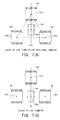
- FIGS. 7(A) and 7(B) are explanatory views each showing an example in which three switch ICs 130 are disposed at positions which are in line symmetry/rotational symmetry with respect to a single thermal fuse 140.
- the centers 130c of the three switch ICs 130 are disposed at positions which are in line symmetry with respect to an axis of symmetry AS passing through the center 140c of the thermal fuse 140.
- the centers 130c of the three switch ICs 130 are disposed at positions which are in rotational symmetry with respect to the center 140c of the thermal fuse 140 and which are located at intervals of 120°.
- FIG. 7(B) although the three switch ICs 130 are disposed at positions which are in line symmetry with respect to the axis of symmetry AS passing through the center 140c of the thermal fuse 140, the three switch ICs 130 are not in rotational symmetry.
- FIGS. 8(A) and 8(B) are explanatory views each showing an example in which four switch ICs 130 are disposed at positions which are in line symmetry or rotational symmetry with respect to a single thermal fuse 140.
- the four switch ICs 130 are disposed at positions which are in line symmetry with respect to two axes of symmetry AS1 and AS2 passing through the center 140c of the thermal fuse 140 and being orthogonal to each other.
- the centers 130c of the four switch ICs 130 are disposed at positions which are in rotational symmetry with respect to the center 140c of the thermal fuse 140 and which are located at intervals of 90°.
- FIGS. 9(A) and 9(B) are explanatory views each showing an example in which four switch ICs 130 are disposed at positions which are in line symmetry with respect to two thermal fuses 140.
- two thermal fuses 140 are disposed at the center, and two switch ICs 130 are disposed on the left and right sides of the thermal fuses 140.
- These four switch ICs 130 are disposed at positions which are in line symmetry with respect to an axis of symmetry AS passing through the centers 140c of the two thermal fuses 140.
- a single thermal fuse 140 is disposed at the center of each pair of two switch ICs 130.
- each of the two thermal fuses 140 provides overheat protection for two switch ICs 130 located on the left and right sides thereof.
- a circuit including two sets each of which is composed of a single thermal fuse 140 and two switch ICs 130 and which are connected in parallel is formed between the power supply input terminal 151 and the load connection terminal 152.
- the layout of the switch ICs 130 and the thermal fuse(s) 140 satisfy one or more of the following conditions.
- Switch ICs 130 and a thermal fuse 140 which provides overheat protection for the switch ICs 130 have a positional relation such that no switch IC 130 is present between any of the switch ICs 130 and the thermal fuse 140 ( FIG. 1 and FIG. 5 though FIGS. 9(A) and 9(B) ).
- the shortest distance between the perimeter of each switch IC 130 and the perimeter of the thermal fuse 140 is smaller than the dimension L2 of each switch IC 130 in the longitudinal direction ( FIG. 1 ).
- the shortest distance between the perimeter of each switch IC 130 and the perimeter of the thermal fuse 140 is smaller than the dimension W2 of each switch IC 130 in the lateral direction ( FIG. 1 ).
- each switch IC 130 is disposed to be located within the circle C4 whose center coincides with the center 140c of the thermal fuse 140 and whose radius is (0.5 ⁇ L1 + 1.5 ⁇ L2) ( FIG. 5 ).
- L1 is the dimension of the thermal fuse 140 in the longitudinal direction
- L2 is the dimension of each switch IC 130 in the longitudinal direction.
- each switch IC 130 is disposed to be located within the circle C3 whose center coincides with the center 140c of the thermal fuse 140 and whose radius is (2 ⁇ R2) ( FIG. 5 ).
- R2 is the radius of the circumscribed circle C2 of each switch IC 130.
- the plurality of switch ICs 130 and the thermal fuse 140 are disposed in such a manner that the inter-center distances D1, D2 ... between the plurality of switch ICs 130 and the thermal fuse 140 fall within the range of ⁇ 30% of the average of the inter-center distances ( FIG. 5 ).
- the plurality of switch ICs 130 are disposed at positions which are in rotational symmetry or line symmetry with respect to the thermal fuse 140 ( FIGS. 6(A) and 6(B) through FIGS. 9(A) and 9(B) )
- the shortest distance between each switch IC 130 and the thermal fuse 140 is equal to or less than 15 mm, or is equal to or less than 10 mm.
- these layout conditions 1 through 8 are conditions when the switch ICs 130 and the thermal fuse 140 are projected in the thickness direction of the printed circuit board 150.
- the plurality of switch ICs 130 are disposed in such a manner that no switch IC 130 is present between any of the switch ICs 130 and the thermal fuse 140, irrespective of which one of the switch ICs 130 breaks, overheating of the broken switch IC 130 can be prevented to substantially the same degree by the thermal fuse 140. Further, when the plurality of switch ICs 130 are disposed to satisfy one or more of the above-mentioned various layout conditions 2 through 8, overheating of each broken switch IC 130 can be prevented more properly.
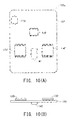
- FIGS. 10(A) and 10(B) are plan and front views of a control apparatus 100b which is another embodiment of the present invention.
- the difference from the control apparatus 100 shown in FIG. 1 is only that, in the control apparatus 100b shown in FIGS. 10(A) and 10(B) , a thermal fuse 140 is disposed on the back surface of a printed circuit board 150, and the remaining configuration is the same as the control apparatus 100 shown in FIG. 1 .
- the control apparatus 100b shown in FIGS. 10(A) and 10(B) also yields effects substantially the same as those of the control apparatus 100 shown in FIG. 1 .
- the switch ICs 130 and the thermal fuse 140 are disposed on different surfaces of the printed circuit board 150, the degree of freedom of layout increases, and the area of the printed circuit board 150 can be decreased.
- FIGS. 11(A) and 11(B) are plan and front views of a control apparatus 100c which is still another embodiment of the present invention.
- the difference from the control apparatus 100b shown in FIGS. 10(A) and 10(B) is only that, in the control apparatus 100c shown in FIGS. 11(A) and 11(B) , two switch ICs 130 are disposed on a printed circuit board 150 such that they are located adjacent to each other, and that a thermal fuse 140a is disposed in a state in which it is in contract with the mold portions of the two switch ICs 130.
- the remaining configuration is the same as the control apparatus 100b shown in FIGS. 10(A) and 10(B) .
- the lead wires 142 of the thermal fuse 140a are connected to pads of the printed circuit board 150 in a state in which the lead wires 142 extend over the switch ICs 130.
- This thermal fuse 140a is a so-called axial component.
- the control apparatus 100c shown in FIGS. 11(A) and 11(B) also yields effects substantially the same as those of the control apparatus 100 shown in FIG. 1 and the control apparatus 100b shown in FIGS. 10 (A) and 10 (B) .
- FIGS. 12(A) and 12(B) are plan and front views of a control apparatus 100d which is still another embodiment of the present invention.
- the difference from the control apparatus 100c shown in FIGS. 11(A) and 11(B) is only that, in the control apparatus 100d shown in FIGS. 12(A) and 12(B) , a surface-mount-type thermal fuse 140 which is the same as that used in the control apparatus 100 shown in FIG. 1 is disposed on the back surface of a printed circuit board 150.
- the remaining configuration is the same as the control apparatus 100c shown in FIGS. 11(A) and 11(B) .
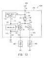
- FIG. 13 is a block diagram showing the configuration of a control apparatus 100e which is still another embodiment of the present invention.
- the difference from the control apparatus 100 shown in FIG. 2 is only that, in the control apparatus 100e shown in FIG. 13 , the output terminals of the individual switch ICs 130 are connected to different resistive loads 300 via different load connection terminals 152 provided on the printed circuit board 150, and the remaining structure is the same as the control apparatus 100 shown in FIG. 2 .
- the individual switch ICs 130 may be used to drive the different resistive loads 300.
- the thermal fuse 140 since the thermal fuse 140 is in common connection with the plurality of switch ICs 130, the thermal fuse 140 can perform overheat protection for the plurality of switch ICs 130.
- the thermal fuse 140 which includes a passive element having a function of interrupting current in response to temperature rise is used as an overheat prevention component.
- an overheat prevention component which includes a passive element having a function of limiting current in response to temperature rise.
- an overheat prevention component using a PTC thermistor can be used as the latter overheat prevention component.
- an overheat prevention component having a function of interrupting current when an unintended current path CP as described with reference to FIG. 4 is formed, such a current path CP can be interrupted.
Landscapes
- Engineering & Computer Science (AREA)
- Microelectronics & Electronic Packaging (AREA)
- Chemical & Material Sciences (AREA)
- Combustion & Propulsion (AREA)
- Mechanical Engineering (AREA)
- General Engineering & Computer Science (AREA)
- Fuses (AREA)
- Structures For Mounting Electric Components On Printed Circuit Boards (AREA)
- Structure Of Printed Boards (AREA)
- Physics & Mathematics (AREA)
- General Physics & Mathematics (AREA)
- Automation & Control Theory (AREA)
Claims (10)
- Appareil de commande (100) dans lequel un circuit intégré de commutation (130) est disposé sur une carte à circuit imprimé (150), le circuit intégré de commutation (130) étant un boîtier de circuit intégré incluant un commutateur à semi-conducteur (131) et étant prévu du côté haute tension d'une charge résistive (300) de façon à attaquer la charge résistive (300), dans lequel
plusieurs circuits intégrés de commutation (130) sont disposés sur la carte à circuit imprimé (150),
un composant de prévention de surchauffe (140) est prévu et est relié en commun avec la pluralité de circuits intégrés de commutation (130), le composant de prévention de surchauffe (140) incluant un élément passif (141) présentant la fonction d'interrompre ou de limiter le courant circulant au travers de la pluralité de circuits intégrés de commutation (130) en réponse à une élévation de température, et
la pluralité de circuits intégrés de commutation (130) est disposée de telle sorte qu'aucun circuit intégré de commutation (130) n'est présent entre l'un quelconque des circuits intégrés de commutation (130) et le composant de prévention de surchauffe (140). - Appareil de commande (100) selon la revendication 1, dans lequel, lorsque la pluralité de circuits intégrés de commutation (130) et le composant de prévention de surchauffe (140) sont projetés dans la direction de l'épaisseur de la carte à circuit imprimé (150), la pluralité de circuits intégrés de commutation (130) est disposée de sorte à ce que le centre (130c) de chaque circuit intégré de commutation (130) soit présent à l'intérieur d'un cercle (C4) dont le centre coïncide avec le centre (140c) du composant de prévention de surchauffe (140) et dont le rayon vaut : (0,5 · L1 + 1,5 · L2), où L1 représente la dimension du composant de prévention de surchauffe (140) dans la direction longitudinale de celui-ci, et où L2 représente la dimension de chaque circuit intégré de commutation (130) dans la direction longitudinale de celui-ci.
- Appareil de commande (100) selon la revendication 2, dans lequel, lorsque la pluralité de circuits intégrés de commutation (130) et le composant de prévention de surchauffe (140) sont projetés dans la direction de l'épaisseur de la carte à circuit imprimé (150), la distance la plus courte entre le périmètre de chaque circuit intégré de commutation (130) et le périmètre du composant de prévention de surchauffe (140) est plus petite que la dimension (L2) de chaque circuit intégré de commutation (130) dans la direction longitudinale de celui-ci.
- Appareil de commande (100) selon l'une quelconque des revendications 1 à 3, dans lequel, lorsque la pluralité de circuits intégrés de commutation (130) et le composant de prévention de surchauffe (140) sont projetés dans la direction de l'épaisseur de la carte à circuit imprimé (150), la distance entre centres, qui représente la distance entre le centre (130c) de l'un quelconque des circuits intégrés de commutation (130) et le centre (140c) du composant de prévention de surchauffe (140), se retrouve dans une plage de ±30 % de la moyenne des distances entre centres par rapport à la pluralité de circuits intégrés de commutation (130).
- Appareil de commande (100) selon l'une quelconque des revendications 1 à 4, dans lequel, lorsque la pluralité de circuits intégrés de commutation (130) et le composant de prévention de surchauffe (140) sont projetés dans la direction de l'épaisseur de la carte à circuit imprimé (150), les centres (130c) de la pluralité de circuits intégrés de commutation (130) sont disposés à des positions qui sont espacées de la même distance du centre (140c) du composant de prévention de surchauffe (140).
- Appareil de commande (100) selon l'une quelconque des revendications 1 à 5, dans lequel, lorsque la pluralité de circuits intégrés de commutation (130) et le composant de prévention de surchauffe (140) sont projetés dans la direction de l'épaisseur de la carte à circuit imprimé (150), la pluralité de circuits intégrés de commutation (130) est disposée à des positions qui sont placées en symétrie de rotation ou en symétrie linéaire par rapport au composant de prévention de surchauffe (140).
- Appareil de commande (100) selon l'une quelconque des revendications 1 à 6, dans lequel
la pluralité de circuits intégrés de commutation (130) et le composant de prévention de surchauffe (140) sont disposés sur une première surface de la carte à circuit imprimé (150), et
le composant de prévention de surchauffe (140) est disposé à une position qui est située entre la pluralité de circuits intégrés de commutation (130). - Appareil de commande (100) selon l'une quelconque des revendications 1 à 6, dans lequel, lorsque la pluralité de circuits intégrés de commutation (130) et le composant de prévention de surchauffe (140) sont projetés dans la direction de l'épaisseur de la carte à circuit imprimé (150), la pluralité de circuits intégrés de commutation (130) et le composant de prévention de surchauffe (140) sont disposés selon une relation de position telle que le contour du composant de prévention de surchauffe (140) et le contour de chaque circuit intégré de commutation (130) se chevauchent partiellement l'un avec l'autre.
- Appareil de commande (100) selon la revendication 8, dans lequel
la pluralité de circuits intégrés de commutation (130) est disposée sur une première surface de la carte à circuit imprimé (150), et
le composant de prévention de surchauffe (140) est disposé sur une seconde surface de la carte à circuit imprimé (150). - Appareil de commande (100) selon l'une quelconque des revendications 1 à 9, dans lequel l'élément passif (141) est un fusible thermique présentant un courant de coupure de 200 A ou plus.
Applications Claiming Priority (1)
| Application Number | Priority Date | Filing Date | Title |
|---|---|---|---|
| JP2014088940A JP6452949B2 (ja) | 2014-04-23 | 2014-04-23 | 制御装置 |
Publications (2)
| Publication Number | Publication Date |
|---|---|
| EP2960489A1 EP2960489A1 (fr) | 2015-12-30 |
| EP2960489B1 true EP2960489B1 (fr) | 2016-11-23 |
Family
ID=52874991
Family Applications (1)
| Application Number | Title | Priority Date | Filing Date |
|---|---|---|---|
| EP15163085.2A Not-in-force EP2960489B1 (fr) | 2014-04-23 | 2015-04-10 | Appareil de contrôle |
Country Status (3)
| Country | Link |
|---|---|
| EP (1) | EP2960489B1 (fr) |
| JP (1) | JP6452949B2 (fr) |
| KR (1) | KR20150122593A (fr) |
Families Citing this family (1)
| Publication number | Priority date | Publication date | Assignee | Title |
|---|---|---|---|---|
| KR102690205B1 (ko) * | 2022-06-29 | 2024-08-06 | 주식회사 제이알솔루텍 | 비대칭 소자의 회로 배치 구조 및 그 회로 기판 구조 |
Family Cites Families (13)
| Publication number | Priority date | Publication date | Assignee | Title |
|---|---|---|---|---|
| JP2526170Y2 (ja) * | 1990-09-30 | 1997-02-19 | スズキ株式会社 | 電子基板回路 |
| GB9508631D0 (en) * | 1995-04-28 | 1995-06-14 | Smiths Industries Ltd | Electrical circuits |
| JPH11330665A (ja) * | 1998-05-15 | 1999-11-30 | Rohm Co Ltd | 回路基板への温度ヒューズの実装構造 |
| US6445277B1 (en) * | 1999-06-22 | 2002-09-03 | Yazaki Corporation | Safety device of electric circuit and process for producing the same |
| JP2004087851A (ja) * | 2002-08-27 | 2004-03-18 | Sanyo Electric Co Ltd | 回路基板およびパック電池 |
| DE102005005549A1 (de) | 2005-02-07 | 2006-08-10 | Robert Bosch Gmbh | Vorrichtung zur Steuerung eines Heizelements in einem Kraftfahrzeug |
| JP4180597B2 (ja) * | 2005-11-09 | 2008-11-12 | 三菱電機株式会社 | 給電回路の異常検出装置 |
| EP1811819B1 (fr) * | 2006-01-19 | 2011-03-23 | Siemens Aktiengesellschaft | Circuit imprimé |
| JP2009117188A (ja) * | 2007-11-07 | 2009-05-28 | Uchihashi Estec Co Ltd | 発熱性回路素子と温度ヒューズとの接続構造及び回路構造 |
| JP5040681B2 (ja) * | 2008-01-28 | 2012-10-03 | 富士電機株式会社 | 半導体スイッチング素子の配線方法 |
| JP2010272215A (ja) * | 2009-05-19 | 2010-12-02 | Panasonic Corp | 電池ユニット |
| JP2011023556A (ja) * | 2009-07-16 | 2011-02-03 | Panasonic Corp | 電池ユニット |
| JP5053337B2 (ja) * | 2009-07-21 | 2012-10-17 | レノボ・シンガポール・プライベート・リミテッド | 蓄電池用保護素子および保護システム |
-
2014
- 2014-04-23 JP JP2014088940A patent/JP6452949B2/ja not_active Expired - Fee Related
-
2015
- 2015-04-10 EP EP15163085.2A patent/EP2960489B1/fr not_active Not-in-force
- 2015-04-20 KR KR1020150055402A patent/KR20150122593A/ko not_active Ceased
Also Published As
| Publication number | Publication date |
|---|---|
| EP2960489A1 (fr) | 2015-12-30 |
| JP2015207728A (ja) | 2015-11-19 |
| KR20150122593A (ko) | 2015-11-02 |
| JP6452949B2 (ja) | 2019-01-16 |
Similar Documents
| Publication | Publication Date | Title |
|---|---|---|
| EP2955848B1 (fr) | Appareil de contrôle | |
| US9899178B2 (en) | Electronic control device including interrupt wire | |
| CN105474542B (zh) | 半导体装置 | |
| CN102630123B (zh) | 包括中断线路的电子控制装置 | |
| US20120200973A1 (en) | Electronic control device including interrupt wire | |
| US9421925B2 (en) | Power device | |
| US9368309B2 (en) | Electronic part and electronic control unit | |
| EP2957762B1 (fr) | Appareil de contrôle | |
| JP6497327B2 (ja) | 給電制御装置 | |
| EP2960489B1 (fr) | Appareil de contrôle | |
| JP4876934B2 (ja) | 電気回路装置 | |
| US7439532B2 (en) | Solid state relay, electronic device, and method for manufacturing solid state relays having a first control terminal, a first output terminal and a second output terminal as lead terminals | |
| WO2012020571A1 (fr) | Circuit électronique | |
| JP2015207519A (ja) | 制御装置 | |
| JP6883460B2 (ja) | 電流遮断装置およびワイヤハーネス | |
| JP2008267305A (ja) | 内燃機関用点火コイルのパワースイッチユニット | |
| KR20250107414A (ko) | 차량 화재 방지 시스템 | |
| WO2025037551A1 (fr) | Dispositif de protection contre les courts-circuits | |
| KR20050106926A (ko) | 저항조절이 용이한 반도체 소자의 정전기 보호회로 | |
| JP2009281235A (ja) | 内燃機関用点火コイルのパワースイッチユニット |
Legal Events
| Date | Code | Title | Description |
|---|---|---|---|
| PUAI | Public reference made under article 153(3) epc to a published international application that has entered the european phase |
Free format text: ORIGINAL CODE: 0009012 |
|
| AK | Designated contracting states |
Kind code of ref document: A1 Designated state(s): AL AT BE BG CH CY CZ DE DK EE ES FI FR GB GR HR HU IE IS IT LI LT LU LV MC MK MT NL NO PL PT RO RS SE SI SK SM TR |
|
| AX | Request for extension of the european patent |
Extension state: BA ME |
|
| 17P | Request for examination filed |
Effective date: 20160208 |
|
| RBV | Designated contracting states (corrected) |
Designated state(s): AL AT BE BG CH CY CZ DE DK EE ES FI FR GB GR HR HU IE IS IT LI LT LU LV MC MK MT NL NO PL PT RO RS SE SI SK SM TR |
|
| RIC1 | Information provided on ipc code assigned before grant |
Ipc: H02H 3/08 20060101ALN20160520BHEP Ipc: H05K 1/02 20060101ALI20160520BHEP Ipc: H03K 17/687 20060101ALI20160520BHEP Ipc: H01H 37/04 20060101ALN20160520BHEP Ipc: H05K 1/18 20060101ALI20160520BHEP Ipc: H02H 5/04 20060101ALN20160520BHEP Ipc: H03K 17/082 20060101ALI20160520BHEP Ipc: H01H 37/76 20060101ALI20160520BHEP Ipc: H03K 17/0812 20060101ALN20160520BHEP Ipc: H03K 17/08 20060101ALN20160520BHEP Ipc: F02P 19/02 20060101AFI20160520BHEP Ipc: H03K 17/18 20060101ALI20160520BHEP |
|
| GRAP | Despatch of communication of intention to grant a patent |
Free format text: ORIGINAL CODE: EPIDOSNIGR1 |
|
| INTG | Intention to grant announced |
Effective date: 20160801 |
|
| GRAS | Grant fee paid |
Free format text: ORIGINAL CODE: EPIDOSNIGR3 |
|
| GRAA | (expected) grant |
Free format text: ORIGINAL CODE: 0009210 |
|
| AK | Designated contracting states |
Kind code of ref document: B1 Designated state(s): AL AT BE BG CH CY CZ DE DK EE ES FI FR GB GR HR HU IE IS IT LI LT LU LV MC MK MT NL NO PL PT RO RS SE SI SK SM TR |
|
| REG | Reference to a national code |
Ref country code: GB Ref legal event code: FG4D |
|
| REG | Reference to a national code |
Ref country code: CH Ref legal event code: EP |
|
| REG | Reference to a national code |
Ref country code: IE Ref legal event code: FG4D |
|
| REG | Reference to a national code |
Ref country code: AT Ref legal event code: REF Ref document number: 848155 Country of ref document: AT Kind code of ref document: T Effective date: 20161215 |
|
| REG | Reference to a national code |
Ref country code: DE Ref legal event code: R096 Ref document number: 602015000779 Country of ref document: DE |
|
| PG25 | Lapsed in a contracting state [announced via postgrant information from national office to epo] |
Ref country code: LV Free format text: LAPSE BECAUSE OF FAILURE TO SUBMIT A TRANSLATION OF THE DESCRIPTION OR TO PAY THE FEE WITHIN THE PRESCRIBED TIME-LIMIT Effective date: 20161123 |
|
| REG | Reference to a national code |
Ref country code: LT Ref legal event code: MG4D Ref country code: FR Ref legal event code: PLFP Year of fee payment: 3 |
|
| REG | Reference to a national code |
Ref country code: NL Ref legal event code: MP Effective date: 20161123 |
|
| REG | Reference to a national code |
Ref country code: AT Ref legal event code: MK05 Ref document number: 848155 Country of ref document: AT Kind code of ref document: T Effective date: 20161123 |
|
| PG25 | Lapsed in a contracting state [announced via postgrant information from national office to epo] |
Ref country code: GR Free format text: LAPSE BECAUSE OF FAILURE TO SUBMIT A TRANSLATION OF THE DESCRIPTION OR TO PAY THE FEE WITHIN THE PRESCRIBED TIME-LIMIT Effective date: 20170224 Ref country code: SE Free format text: LAPSE BECAUSE OF FAILURE TO SUBMIT A TRANSLATION OF THE DESCRIPTION OR TO PAY THE FEE WITHIN THE PRESCRIBED TIME-LIMIT Effective date: 20161123 Ref country code: NO Free format text: LAPSE BECAUSE OF FAILURE TO SUBMIT A TRANSLATION OF THE DESCRIPTION OR TO PAY THE FEE WITHIN THE PRESCRIBED TIME-LIMIT Effective date: 20170223 Ref country code: NL Free format text: LAPSE BECAUSE OF FAILURE TO SUBMIT A TRANSLATION OF THE DESCRIPTION OR TO PAY THE FEE WITHIN THE PRESCRIBED TIME-LIMIT Effective date: 20161123 Ref country code: LT Free format text: LAPSE BECAUSE OF FAILURE TO SUBMIT A TRANSLATION OF THE DESCRIPTION OR TO PAY THE FEE WITHIN THE PRESCRIBED TIME-LIMIT Effective date: 20161123 |
|
| PG25 | Lapsed in a contracting state [announced via postgrant information from national office to epo] |
Ref country code: RS Free format text: LAPSE BECAUSE OF FAILURE TO SUBMIT A TRANSLATION OF THE DESCRIPTION OR TO PAY THE FEE WITHIN THE PRESCRIBED TIME-LIMIT Effective date: 20161123 Ref country code: FI Free format text: LAPSE BECAUSE OF FAILURE TO SUBMIT A TRANSLATION OF THE DESCRIPTION OR TO PAY THE FEE WITHIN THE PRESCRIBED TIME-LIMIT Effective date: 20161123 Ref country code: PT Free format text: LAPSE BECAUSE OF FAILURE TO SUBMIT A TRANSLATION OF THE DESCRIPTION OR TO PAY THE FEE WITHIN THE PRESCRIBED TIME-LIMIT Effective date: 20170323 Ref country code: ES Free format text: LAPSE BECAUSE OF FAILURE TO SUBMIT A TRANSLATION OF THE DESCRIPTION OR TO PAY THE FEE WITHIN THE PRESCRIBED TIME-LIMIT Effective date: 20161123 Ref country code: PL Free format text: LAPSE BECAUSE OF FAILURE TO SUBMIT A TRANSLATION OF THE DESCRIPTION OR TO PAY THE FEE WITHIN THE PRESCRIBED TIME-LIMIT Effective date: 20161123 Ref country code: AT Free format text: LAPSE BECAUSE OF FAILURE TO SUBMIT A TRANSLATION OF THE DESCRIPTION OR TO PAY THE FEE WITHIN THE PRESCRIBED TIME-LIMIT Effective date: 20161123 Ref country code: HR Free format text: LAPSE BECAUSE OF FAILURE TO SUBMIT A TRANSLATION OF THE DESCRIPTION OR TO PAY THE FEE WITHIN THE PRESCRIBED TIME-LIMIT Effective date: 20161123 |
|
| PG25 | Lapsed in a contracting state [announced via postgrant information from national office to epo] |
Ref country code: CZ Free format text: LAPSE BECAUSE OF FAILURE TO SUBMIT A TRANSLATION OF THE DESCRIPTION OR TO PAY THE FEE WITHIN THE PRESCRIBED TIME-LIMIT Effective date: 20161123 Ref country code: RO Free format text: LAPSE BECAUSE OF FAILURE TO SUBMIT A TRANSLATION OF THE DESCRIPTION OR TO PAY THE FEE WITHIN THE PRESCRIBED TIME-LIMIT Effective date: 20161123 Ref country code: SK Free format text: LAPSE BECAUSE OF FAILURE TO SUBMIT A TRANSLATION OF THE DESCRIPTION OR TO PAY THE FEE WITHIN THE PRESCRIBED TIME-LIMIT Effective date: 20161123 Ref country code: DK Free format text: LAPSE BECAUSE OF FAILURE TO SUBMIT A TRANSLATION OF THE DESCRIPTION OR TO PAY THE FEE WITHIN THE PRESCRIBED TIME-LIMIT Effective date: 20161123 Ref country code: EE Free format text: LAPSE BECAUSE OF FAILURE TO SUBMIT A TRANSLATION OF THE DESCRIPTION OR TO PAY THE FEE WITHIN THE PRESCRIBED TIME-LIMIT Effective date: 20161123 |
|
| REG | Reference to a national code |
Ref country code: DE Ref legal event code: R097 Ref document number: 602015000779 Country of ref document: DE |
|
| PG25 | Lapsed in a contracting state [announced via postgrant information from national office to epo] |
Ref country code: SM Free format text: LAPSE BECAUSE OF FAILURE TO SUBMIT A TRANSLATION OF THE DESCRIPTION OR TO PAY THE FEE WITHIN THE PRESCRIBED TIME-LIMIT Effective date: 20161123 Ref country code: BG Free format text: LAPSE BECAUSE OF FAILURE TO SUBMIT A TRANSLATION OF THE DESCRIPTION OR TO PAY THE FEE WITHIN THE PRESCRIBED TIME-LIMIT Effective date: 20170223 Ref country code: BE Free format text: LAPSE BECAUSE OF FAILURE TO SUBMIT A TRANSLATION OF THE DESCRIPTION OR TO PAY THE FEE WITHIN THE PRESCRIBED TIME-LIMIT Effective date: 20161123 |
|
| PLBE | No opposition filed within time limit |
Free format text: ORIGINAL CODE: 0009261 |
|
| STAA | Information on the status of an ep patent application or granted ep patent |
Free format text: STATUS: NO OPPOSITION FILED WITHIN TIME LIMIT |
|
| 26N | No opposition filed |
Effective date: 20170824 |
|
| PG25 | Lapsed in a contracting state [announced via postgrant information from national office to epo] |
Ref country code: SI Free format text: LAPSE BECAUSE OF FAILURE TO SUBMIT A TRANSLATION OF THE DESCRIPTION OR TO PAY THE FEE WITHIN THE PRESCRIBED TIME-LIMIT Effective date: 20161123 |
|
| REG | Reference to a national code |
Ref country code: IE Ref legal event code: MM4A |
|
| PG25 | Lapsed in a contracting state [announced via postgrant information from national office to epo] |
Ref country code: MC Free format text: LAPSE BECAUSE OF FAILURE TO SUBMIT A TRANSLATION OF THE DESCRIPTION OR TO PAY THE FEE WITHIN THE PRESCRIBED TIME-LIMIT Effective date: 20161123 |
|
| PG25 | Lapsed in a contracting state [announced via postgrant information from national office to epo] |
Ref country code: LU Free format text: LAPSE BECAUSE OF NON-PAYMENT OF DUE FEES Effective date: 20170410 |
|
| REG | Reference to a national code |
Ref country code: FR Ref legal event code: PLFP Year of fee payment: 4 |
|
| PG25 | Lapsed in a contracting state [announced via postgrant information from national office to epo] |
Ref country code: IE Free format text: LAPSE BECAUSE OF NON-PAYMENT OF DUE FEES Effective date: 20170410 |
|
| PG25 | Lapsed in a contracting state [announced via postgrant information from national office to epo] |
Ref country code: MT Free format text: LAPSE BECAUSE OF NON-PAYMENT OF DUE FEES Effective date: 20170410 |
|
| REG | Reference to a national code |
Ref country code: CH Ref legal event code: PL |
|
| PG25 | Lapsed in a contracting state [announced via postgrant information from national office to epo] |
Ref country code: LI Free format text: LAPSE BECAUSE OF NON-PAYMENT OF DUE FEES Effective date: 20180430 Ref country code: CH Free format text: LAPSE BECAUSE OF NON-PAYMENT OF DUE FEES Effective date: 20180430 |
|
| PG25 | Lapsed in a contracting state [announced via postgrant information from national office to epo] |
Ref country code: HU Free format text: LAPSE BECAUSE OF FAILURE TO SUBMIT A TRANSLATION OF THE DESCRIPTION OR TO PAY THE FEE WITHIN THE PRESCRIBED TIME-LIMIT; INVALID AB INITIO Effective date: 20150410 |
|
| PG25 | Lapsed in a contracting state [announced via postgrant information from national office to epo] |
Ref country code: CY Free format text: LAPSE BECAUSE OF FAILURE TO SUBMIT A TRANSLATION OF THE DESCRIPTION OR TO PAY THE FEE WITHIN THE PRESCRIBED TIME-LIMIT Effective date: 20161123 |
|
| PG25 | Lapsed in a contracting state [announced via postgrant information from national office to epo] |
Ref country code: MK Free format text: LAPSE BECAUSE OF FAILURE TO SUBMIT A TRANSLATION OF THE DESCRIPTION OR TO PAY THE FEE WITHIN THE PRESCRIBED TIME-LIMIT Effective date: 20161123 |
|
| GBPC | Gb: european patent ceased through non-payment of renewal fee |
Effective date: 20190410 |
|
| PG25 | Lapsed in a contracting state [announced via postgrant information from national office to epo] |
Ref country code: GB Free format text: LAPSE BECAUSE OF NON-PAYMENT OF DUE FEES Effective date: 20190410 |
|
| PG25 | Lapsed in a contracting state [announced via postgrant information from national office to epo] |
Ref country code: TR Free format text: LAPSE BECAUSE OF FAILURE TO SUBMIT A TRANSLATION OF THE DESCRIPTION OR TO PAY THE FEE WITHIN THE PRESCRIBED TIME-LIMIT Effective date: 20161123 |
|
| PG25 | Lapsed in a contracting state [announced via postgrant information from national office to epo] |
Ref country code: AL Free format text: LAPSE BECAUSE OF FAILURE TO SUBMIT A TRANSLATION OF THE DESCRIPTION OR TO PAY THE FEE WITHIN THE PRESCRIBED TIME-LIMIT Effective date: 20161123 Ref country code: IS Free format text: LAPSE BECAUSE OF FAILURE TO SUBMIT A TRANSLATION OF THE DESCRIPTION OR TO PAY THE FEE WITHIN THE PRESCRIBED TIME-LIMIT Effective date: 20170323 |
|
| PGFP | Annual fee paid to national office [announced via postgrant information from national office to epo] |
Ref country code: IT Payment date: 20210310 Year of fee payment: 7 Ref country code: FR Payment date: 20210309 Year of fee payment: 7 |
|
| PG25 | Lapsed in a contracting state [announced via postgrant information from national office to epo] |
Ref country code: FR Free format text: LAPSE BECAUSE OF NON-PAYMENT OF DUE FEES Effective date: 20220430 |
|
| PG25 | Lapsed in a contracting state [announced via postgrant information from national office to epo] |
Ref country code: IT Free format text: LAPSE BECAUSE OF NON-PAYMENT OF DUE FEES Effective date: 20220410 |
|
| PGFP | Annual fee paid to national office [announced via postgrant information from national office to epo] |
Ref country code: DE Payment date: 20230228 Year of fee payment: 9 |
|
| REG | Reference to a national code |
Ref country code: DE Ref legal event code: R081 Ref document number: 602015000779 Country of ref document: DE Owner name: NITERRA CO., LTD., NAGOYA-SHI, JP Free format text: FORMER OWNER: NGK SPARK PLUG CO., LTD., NAGOYA-SHI, AICHI, JP |
|
| REG | Reference to a national code |
Ref country code: DE Ref legal event code: R119 Ref document number: 602015000779 Country of ref document: DE |
|
| PG25 | Lapsed in a contracting state [announced via postgrant information from national office to epo] |
Ref country code: DE Free format text: LAPSE BECAUSE OF NON-PAYMENT OF DUE FEES Effective date: 20241105 |
|
| PG25 | Lapsed in a contracting state [announced via postgrant information from national office to epo] |
Ref country code: DE Free format text: LAPSE BECAUSE OF NON-PAYMENT OF DUE FEES Effective date: 20241105 |