EP2964418B1 - Système et procédé d'impression 3d à base de diode de grande puissance - Google Patents
Système et procédé d'impression 3d à base de diode de grande puissance Download PDFInfo
- Publication number
- EP2964418B1 EP2964418B1 EP14760359.1A EP14760359A EP2964418B1 EP 2964418 B1 EP2964418 B1 EP 2964418B1 EP 14760359 A EP14760359 A EP 14760359A EP 2964418 B1 EP2964418 B1 EP 2964418B1
- Authority
- EP
- European Patent Office
- Prior art keywords
- optical signal
- substrate
- mask
- liquid crystal
- layer
- Prior art date
- Legal status (The legal status is an assumption and is not a legal conclusion. Google has not performed a legal analysis and makes no representation as to the accuracy of the status listed.)
- Active
Links
Images


Classifications
-
- B—PERFORMING OPERATIONS; TRANSPORTING
- B29—WORKING OF PLASTICS; WORKING OF SUBSTANCES IN A PLASTIC STATE IN GENERAL
- B29C—SHAPING OR JOINING OF PLASTICS; SHAPING OF MATERIAL IN A PLASTIC STATE, NOT OTHERWISE PROVIDED FOR; AFTER-TREATMENT OF THE SHAPED PRODUCTS, e.g. REPAIRING
- B29C64/00—Additive manufacturing, i.e. manufacturing of three-dimensional [3D] objects by additive deposition, additive agglomeration or additive layering, e.g. by 3D printing, stereolithography or selective laser sintering
- B29C64/10—Processes of additive manufacturing
- B29C64/141—Processes of additive manufacturing using only solid materials
- B29C64/153—Processes of additive manufacturing using only solid materials using layers of powder being selectively joined, e.g. by selective laser sintering or melting
-
- B—PERFORMING OPERATIONS; TRANSPORTING
- B22—CASTING; POWDER METALLURGY
- B22F—WORKING METALLIC POWDER; MANUFACTURE OF ARTICLES FROM METALLIC POWDER; MAKING METALLIC POWDER; APPARATUS OR DEVICES SPECIALLY ADAPTED FOR METALLIC POWDER
- B22F10/00—Additive manufacturing of workpieces or articles from metallic powder
- B22F10/20—Direct sintering or melting
- B22F10/28—Powder bed fusion, e.g. selective laser melting [SLM] or electron beam melting [EBM]
-
- B—PERFORMING OPERATIONS; TRANSPORTING
- B22—CASTING; POWDER METALLURGY
- B22F—WORKING METALLIC POWDER; MANUFACTURE OF ARTICLES FROM METALLIC POWDER; MAKING METALLIC POWDER; APPARATUS OR DEVICES SPECIALLY ADAPTED FOR METALLIC POWDER
- B22F10/00—Additive manufacturing of workpieces or articles from metallic powder
- B22F10/30—Process control
- B22F10/36—Process control of energy beam parameters
- B22F10/366—Scanning parameters, e.g. hatch distance or scanning strategy
-
- B—PERFORMING OPERATIONS; TRANSPORTING
- B22—CASTING; POWDER METALLURGY
- B22F—WORKING METALLIC POWDER; MANUFACTURE OF ARTICLES FROM METALLIC POWDER; MAKING METALLIC POWDER; APPARATUS OR DEVICES SPECIALLY ADAPTED FOR METALLIC POWDER
- B22F12/00—Apparatus or devices specially adapted for additive manufacturing; Auxiliary means for additive manufacturing; Combinations of additive manufacturing apparatus or devices with other processing apparatus or devices
- B22F12/40—Radiation means
- B22F12/41—Radiation means characterised by the type, e.g. laser or electron beam
- B22F12/43—Radiation means characterised by the type, e.g. laser or electron beam pulsed; frequency modulated
-
- B—PERFORMING OPERATIONS; TRANSPORTING
- B22—CASTING; POWDER METALLURGY
- B22F—WORKING METALLIC POWDER; MANUFACTURE OF ARTICLES FROM METALLIC POWDER; MAKING METALLIC POWDER; APPARATUS OR DEVICES SPECIALLY ADAPTED FOR METALLIC POWDER
- B22F12/00—Apparatus or devices specially adapted for additive manufacturing; Auxiliary means for additive manufacturing; Combinations of additive manufacturing apparatus or devices with other processing apparatus or devices
- B22F12/40—Radiation means
- B22F12/44—Radiation means characterised by the configuration of the radiation means
-
- B—PERFORMING OPERATIONS; TRANSPORTING
- B23—MACHINE TOOLS; METAL-WORKING NOT OTHERWISE PROVIDED FOR
- B23K—SOLDERING OR UNSOLDERING; WELDING; CLADDING OR PLATING BY SOLDERING OR WELDING; CUTTING BY APPLYING HEAT LOCALLY, e.g. FLAME CUTTING; WORKING BY LASER BEAM
- B23K26/00—Working by laser beam, e.g. welding, cutting or boring
- B23K26/02—Positioning or observing the workpiece, e.g. with respect to the point of impact; Aligning, aiming or focusing the laser beam
- B23K26/04—Automatically aligning, aiming or focusing the laser beam, e.g. using the back-scattered light
- B23K26/042—Automatically aligning the laser beam
-
- B—PERFORMING OPERATIONS; TRANSPORTING
- B23—MACHINE TOOLS; METAL-WORKING NOT OTHERWISE PROVIDED FOR
- B23K—SOLDERING OR UNSOLDERING; WELDING; CLADDING OR PLATING BY SOLDERING OR WELDING; CUTTING BY APPLYING HEAT LOCALLY, e.g. FLAME CUTTING; WORKING BY LASER BEAM
- B23K26/00—Working by laser beam, e.g. welding, cutting or boring
- B23K26/02—Positioning or observing the workpiece, e.g. with respect to the point of impact; Aligning, aiming or focusing the laser beam
- B23K26/06—Shaping the laser beam, e.g. by masks or multi-focusing
- B23K26/062—Shaping the laser beam, e.g. by masks or multi-focusing by direct control of the laser beam
- B23K26/0622—Shaping the laser beam, e.g. by masks or multi-focusing by direct control of the laser beam by shaping pulses
-
- B—PERFORMING OPERATIONS; TRANSPORTING
- B23—MACHINE TOOLS; METAL-WORKING NOT OTHERWISE PROVIDED FOR
- B23K—SOLDERING OR UNSOLDERING; WELDING; CLADDING OR PLATING BY SOLDERING OR WELDING; CUTTING BY APPLYING HEAT LOCALLY, e.g. FLAME CUTTING; WORKING BY LASER BEAM
- B23K26/00—Working by laser beam, e.g. welding, cutting or boring
- B23K26/02—Positioning or observing the workpiece, e.g. with respect to the point of impact; Aligning, aiming or focusing the laser beam
- B23K26/06—Shaping the laser beam, e.g. by masks or multi-focusing
- B23K26/064—Shaping the laser beam, e.g. by masks or multi-focusing by means of optical elements, e.g. lenses, mirrors or prisms
- B23K26/0643—Shaping the laser beam, e.g. by masks or multi-focusing by means of optical elements, e.g. lenses, mirrors or prisms comprising mirrors
-
- B—PERFORMING OPERATIONS; TRANSPORTING
- B23—MACHINE TOOLS; METAL-WORKING NOT OTHERWISE PROVIDED FOR
- B23K—SOLDERING OR UNSOLDERING; WELDING; CLADDING OR PLATING BY SOLDERING OR WELDING; CUTTING BY APPLYING HEAT LOCALLY, e.g. FLAME CUTTING; WORKING BY LASER BEAM
- B23K26/00—Working by laser beam, e.g. welding, cutting or boring
- B23K26/02—Positioning or observing the workpiece, e.g. with respect to the point of impact; Aligning, aiming or focusing the laser beam
- B23K26/06—Shaping the laser beam, e.g. by masks or multi-focusing
- B23K26/064—Shaping the laser beam, e.g. by masks or multi-focusing by means of optical elements, e.g. lenses, mirrors or prisms
- B23K26/066—Shaping the laser beam, e.g. by masks or multi-focusing by means of optical elements, e.g. lenses, mirrors or prisms by using masks
-
- B—PERFORMING OPERATIONS; TRANSPORTING
- B23—MACHINE TOOLS; METAL-WORKING NOT OTHERWISE PROVIDED FOR
- B23K—SOLDERING OR UNSOLDERING; WELDING; CLADDING OR PLATING BY SOLDERING OR WELDING; CUTTING BY APPLYING HEAT LOCALLY, e.g. FLAME CUTTING; WORKING BY LASER BEAM
- B23K26/00—Working by laser beam, e.g. welding, cutting or boring
- B23K26/14—Working by laser beam, e.g. welding, cutting or boring using a fluid stream, e.g. a jet of gas, in conjunction with the laser beam; Nozzles therefor
- B23K26/144—Working by laser beam, e.g. welding, cutting or boring using a fluid stream, e.g. a jet of gas, in conjunction with the laser beam; Nozzles therefor the fluid stream containing particles, e.g. powder
-
- B—PERFORMING OPERATIONS; TRANSPORTING
- B23—MACHINE TOOLS; METAL-WORKING NOT OTHERWISE PROVIDED FOR
- B23K—SOLDERING OR UNSOLDERING; WELDING; CLADDING OR PLATING BY SOLDERING OR WELDING; CUTTING BY APPLYING HEAT LOCALLY, e.g. FLAME CUTTING; WORKING BY LASER BEAM
- B23K26/00—Working by laser beam, e.g. welding, cutting or boring
- B23K26/34—Laser welding for purposes other than joining
- B23K26/342—Build-up welding
-
- B—PERFORMING OPERATIONS; TRANSPORTING
- B33—ADDITIVE MANUFACTURING TECHNOLOGY
- B33Y—ADDITIVE MANUFACTURING, i.e. MANUFACTURING OF THREE-DIMENSIONAL [3D] OBJECTS BY ADDITIVE DEPOSITION, ADDITIVE AGGLOMERATION OR ADDITIVE LAYERING, e.g. BY 3D PRINTING, STEREOLITHOGRAPHY OR SELECTIVE LASER SINTERING
- B33Y10/00—Processes of additive manufacturing
-
- B—PERFORMING OPERATIONS; TRANSPORTING
- B33—ADDITIVE MANUFACTURING TECHNOLOGY
- B33Y—ADDITIVE MANUFACTURING, i.e. MANUFACTURING OF THREE-DIMENSIONAL [3D] OBJECTS BY ADDITIVE DEPOSITION, ADDITIVE AGGLOMERATION OR ADDITIVE LAYERING, e.g. BY 3D PRINTING, STEREOLITHOGRAPHY OR SELECTIVE LASER SINTERING
- B33Y30/00—Apparatus for additive manufacturing; Details thereof or accessories therefor
-
- B—PERFORMING OPERATIONS; TRANSPORTING
- B33—ADDITIVE MANUFACTURING TECHNOLOGY
- B33Y—ADDITIVE MANUFACTURING, i.e. MANUFACTURING OF THREE-DIMENSIONAL [3D] OBJECTS BY ADDITIVE DEPOSITION, ADDITIVE AGGLOMERATION OR ADDITIVE LAYERING, e.g. BY 3D PRINTING, STEREOLITHOGRAPHY OR SELECTIVE LASER SINTERING
- B33Y80/00—Products made by additive manufacturing
-
- B—PERFORMING OPERATIONS; TRANSPORTING
- B22—CASTING; POWDER METALLURGY
- B22F—WORKING METALLIC POWDER; MANUFACTURE OF ARTICLES FROM METALLIC POWDER; MAKING METALLIC POWDER; APPARATUS OR DEVICES SPECIALLY ADAPTED FOR METALLIC POWDER
- B22F10/00—Additive manufacturing of workpieces or articles from metallic powder
- B22F10/30—Process control
-
- B—PERFORMING OPERATIONS; TRANSPORTING
- B22—CASTING; POWDER METALLURGY
- B22F—WORKING METALLIC POWDER; MANUFACTURE OF ARTICLES FROM METALLIC POWDER; MAKING METALLIC POWDER; APPARATUS OR DEVICES SPECIALLY ADAPTED FOR METALLIC POWDER
- B22F12/00—Apparatus or devices specially adapted for additive manufacturing; Auxiliary means for additive manufacturing; Combinations of additive manufacturing apparatus or devices with other processing apparatus or devices
- B22F12/50—Means for feeding of material, e.g. heads
- B22F12/55—Two or more means for feeding material
-
- B—PERFORMING OPERATIONS; TRANSPORTING
- B22—CASTING; POWDER METALLURGY
- B22F—WORKING METALLIC POWDER; MANUFACTURE OF ARTICLES FROM METALLIC POWDER; MAKING METALLIC POWDER; APPARATUS OR DEVICES SPECIALLY ADAPTED FOR METALLIC POWDER
- B22F2998/00—Supplementary information concerning processes or compositions relating to powder metallurgy
- B22F2998/10—Processes characterised by the sequence of their steps
-
- B—PERFORMING OPERATIONS; TRANSPORTING
- B22—CASTING; POWDER METALLURGY
- B22F—WORKING METALLIC POWDER; MANUFACTURE OF ARTICLES FROM METALLIC POWDER; MAKING METALLIC POWDER; APPARATUS OR DEVICES SPECIALLY ADAPTED FOR METALLIC POWDER
- B22F2999/00—Aspects linked to processes or compositions used in powder metallurgy
-
- B—PERFORMING OPERATIONS; TRANSPORTING
- B33—ADDITIVE MANUFACTURING TECHNOLOGY
- B33Y—ADDITIVE MANUFACTURING, i.e. MANUFACTURING OF THREE-DIMENSIONAL [3D] OBJECTS BY ADDITIVE DEPOSITION, ADDITIVE AGGLOMERATION OR ADDITIVE LAYERING, e.g. BY 3D PRINTING, STEREOLITHOGRAPHY OR SELECTIVE LASER SINTERING
- B33Y50/00—Data acquisition or data processing for additive manufacturing
- B33Y50/02—Data acquisition or data processing for additive manufacturing for controlling or regulating additive manufacturing processes
-
- Y—GENERAL TAGGING OF NEW TECHNOLOGICAL DEVELOPMENTS; GENERAL TAGGING OF CROSS-SECTIONAL TECHNOLOGIES SPANNING OVER SEVERAL SECTIONS OF THE IPC; TECHNICAL SUBJECTS COVERED BY FORMER USPC CROSS-REFERENCE ART COLLECTIONS [XRACs] AND DIGESTS
- Y02—TECHNOLOGIES OR APPLICATIONS FOR MITIGATION OR ADAPTATION AGAINST CLIMATE CHANGE
- Y02P—CLIMATE CHANGE MITIGATION TECHNOLOGIES IN THE PRODUCTION OR PROCESSING OF GOODS
- Y02P10/00—Technologies related to metal processing
- Y02P10/25—Process efficiency
Definitions
- the present disclosure relates to Additive Manufacturing systems and techniques for making three dimensional articles and parts, and more particularly to a system and method for performing Additive Manufacturing using a high power diode system.
- Metal AM requires a relatively high power, highly focused laser beam (typically on the order of 100W-1000W) to melt, fuse, and/or sinter metallic powder.
- the metal powder is typically placed in a powder bed during the AM process.
- the laser beam is rastered along the powder surface to make a two-dimensional section per pass. Once each layer is completed, the powder bed retracts and new powder is layered on top of the just-completed layer.
- US 2011/0190904 A1 provides a method and a system for fabricating multimaterial bodies in a layer-wise fashion. These bodies may be used for bone stabilizing implants. A conventional mask to block certain portions of optical energy from reaching the beneath layer of material is furthermore disclosed.
- US 2009/020901 A1 relates to the additive manufacture of parts in powder beds, wherein a LCD mask for directing energy beam radiations at desired locations to melt the powder might be used.
- US 2004/0200812 A1 teaches a laser imaging apparatus having a laser source outputting a laser beam and an electronic display device.
- the electronic display device is positioned downstream from the laser source and operable to selectively polarize parts of the laser beam.
- the present disclosure further relates to a system for performing an Additive Manufacturing (AM) fabrication process on a powdered material forming a substrate.
- the system comprises a diode array for generating a pulsed optical signal sufficient in optical intensity to melt or sinter a powdered material of the substrate.
- a mask is interposed between the diode array and the substrate for preventing a first predetermined portion of the pulsed optical signal from reaching the substrate, while allowing a second predetermined portion to reach the substrate.
- the mask is configured to be controlled and addressable by a processor to electronically enable selected subportions of the substrate to be masked off.
- a processor is used for electronically controlling the mask.
- the present disclosure relates to a method for performing Additive Manufacturing (AM).
- the method comprises irradiating a powdered layer of a substrate using a pulsed optical signal sufficient to irradiate at least a substantial portion of an entire two dimensional layer within which the substrate is positioned.
- a mask is used to selectively block a first subportion of the pulsed optical signal from reaching the first layer of the substrate.
- a second layer of powdered material is placed over the first layer. The second layer is irradiated using the pulsed optical signal while using the mask to selectively block a second subportion of the pulsed optical signal from reaching the second layer of the substrate.
- Selectively electronically controlling the mask 14 with the computer 18 allows the optical beam from the diode array 12 to be prevented from reaching specific selected portions of powder that forms a substrate 20 (i.e., powder bed) so that those portions are not irradiated by the beam.
- portion 15 is cross hatched to represent a portion of the output from the diode array 12 that does not reach the powdered material of the substrate 20.
- the diode array 12 may comprise a single large diode bar. Alternatively a plurality of diode bars located adjacent one another may be used to form the diode array 12. In one preferred form the diode array may be made up of arrays of diode bars each being about 1cm x 0.015cm to construct a 25cm x 25cm diode array. However, any number of diode bars may be used, and the precise number and configuration may depend on the part being constructed as well as other factors. Suitable diode bars for forming the diode array 12 are available from Lasertel of Arlington, AZ, Oclaro Inc. of San Jose, CA, nLight Corp. of Vancouver, WA, Quantel Inc.
- the diode array 12 is able to provide a minimum power density of about 10kW/cm 2 and maximum > 100 kW/cm 2 at two percent duty cycle. This makes it feasible to generate sufficient optical power to melt a wide variety of materials.
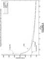
- Figure 3 provides a table of the average power flux that has been calculated to melt various types of materials.
- Figure 4 shows a graph that illustrates the effectiveness of the diode array 12 on a variety of metal powders (i.e., Aluminum, Titanium, Iron and Tungsten), at a power flux sufficient to melt all the materials. The calculations to obtain the graphs shown in Figure 4 were performed in MATLAB with conductive and radiative losses taken into account. A conservative 30% absorptivity was assumed along with a powder layer thickness of 100 ⁇ m.
- diode arrays comprised of one or more diode bars
- the diode array 12 may be constructed to have a one square meter area, which would allow correspondingly large scale components to be constructed through an AM fabrication process, provided of course that a suitably sized powder bed is available to support fabrication of the part.
- the system 10 can be integrated into existing AM fabrication systems with the added benefit of no moving parts.
- the system 10 allows for the AM fabrication of traditionally difficult to fabricate and join metal such as ODS (oxide dispersion strengthened) steels or any alloy traditionally formed using solid state (i.e. non-melt) processing techniques.
- the mask 14 forms a "liquid crystal polarization rotator" comprised of a liquid crystal module (LCM) 14a and a polarizing element 14b, in this example a polarizing mirror (hereinafter "polarizing mirror” 14b).
- the polarizing mirror 14b directs the light defined by the liquid crystal polarization rotator and shapes the optical pattern that irradiates the substrate 20.
- the LCM 14a that helps to form the mask 14 may is up of one or more two dimensional, electronically (i.e., digitally) addressable arrays of pixels.
- Liquid crystal polarizers are commercially available and form two dimensional arrays of addressable pixels which work by changing the polarity of an incoming photon that is then rejected by a polarization element.
- the polarizing element 14b forms a discrete component of the mask 14 that is used to help focus and/or shape the optical signal.
- a first layer of powdered material is acted on by the system by pulsing the diode array 12 to melt selected portions (or possibly the entire portion) of the first layer.
- a subsequent (i.e., second) layer of powdered material is added over the layer just acted on by the system 10 and the process is repeated.
- the diode array 12 is pulsed to melt one or more selected subportions (or possibly the entirety) of the second layer of material.
- the system 10 electronically controls the pixels of the mask 14 to selectively block specific, predetermined portions of the substrate 20 from being irradiated by the pulsed optical signal from the diode array 12.
- This process is repeated for each layer, with the computer 18 controlling the mask 14 so that, for each layer, one or more selected subportions (or possibly the entirety) of the powdered material is blocked by the mask 14 from being exposed to the pulsed optical signal.
- the computer 18 controlling the mask 14 so that, for each layer, one or more selected subportions (or possibly the entirety) of the powdered material is blocked by the mask 14 from being exposed to the pulsed optical signal.
- an entire two dimensional area of each layer is melted or sintered at once by pulsing the diode array 12.
- System 100 includes a diode array 102 and a diode relay telescope 104.
- the diode relay telescope 104 is used to provide digital control over "tiles" within an array image to the "pixels" in the substrate 20 (powder bed).
- Figure 6 illustrates a system 200 having a diode array 202 and a plurality of focusing lenses 206 that are used to focus the optical energy from the array onto a corresponding plurality of "sheets" representing the substrate 20.
- the systems 10, 100 and 200 are able to melt and sinter each layer in a single "pass" or, put differently, in a single operation by pulsing the diode array 12.
- the need to raster scan an optical beam dozens, hundreds or more times, back and forth across a surface, is therefore eliminated. This significantly reduces the time required to melt and sinter each layer of powder material during the AM fabrication process.
- Nozzles 301, 302, and 303 are capable of depositing layers of different material powders 304 onto the substrate 20.
- the nozzle heads 301, 302 and 303 are rastered across the part surface covering it with material addressed by a programmable source. Both the irradiation from the diode array 12 and operation of the mask 14, as described in connection with the system 10, can be controlled such that each material deposited from the nozzles 301, 302 and 303 receives the correct amount of optical energy for a controlled melt or sintering.
Landscapes
- Engineering & Computer Science (AREA)
- Physics & Mathematics (AREA)
- Optics & Photonics (AREA)
- Chemical & Material Sciences (AREA)
- Materials Engineering (AREA)
- Manufacturing & Machinery (AREA)
- Plasma & Fusion (AREA)
- Mechanical Engineering (AREA)
- Health & Medical Sciences (AREA)
- General Health & Medical Sciences (AREA)
- Toxicology (AREA)
- Automation & Control Theory (AREA)
- Powder Metallurgy (AREA)
- Metallurgy (AREA)
- Organic Chemistry (AREA)
- General Physics & Mathematics (AREA)
Claims (8)
- Système pour réaliser un procédé de fabrication additive (AM) sur un matériau pulvérulent formant un substrat, le système comprenant :Une matrice de diodes pour générer un signal optique suffisant pour faire fondre ou fritter un matériau pulvérulent du substrat ;un masque pour recevoir le signal optique généré par la matrice de diodes, le masque formant un rotateur de polarisation à cristaux liquides, le rotateur de polarisation à cristaux liquides incluant un module à cristaux liquides et un polariseur, dans lequel le module à cristaux liquides fonctionne pour recevoir et pour mettre en rotation une première portion du signal optique passant à travers celui-ci tout en permettant à une seconde portion du signal optique de passer à travers celui-ci sans être mise en rotation, et dans lequel le polariseur, qui comprend un miroir polarisant, fonctionne pour rejeter, en réfléchissant, une des première et seconde portions du signal optique reçu du module à cristaux liquides, et ainsi empêcher l'une des première et seconde portions d'atteindre le substrat, alors que le polariseur permet à l'autre des première et seconde portions du signal optique d'atteindre le substrat, le module à cristaux liquides du masque ayant une pluralité de pixels, agencés en un motif bidimensionnel, qui sont individuellement commandés pour permettre au masque de masquer une ou plusieurs zones sélectionnées d'une couche spécifique du matériau pulvérulent du substrat, et dans lequel le masque n'absorbe sensiblement aucune énergie optique provenant du signal optique ; etau moins un processeur commandant une sortie de la matrice de diodes et assistant dans la commande du fonctionnement du masque de telle sorte que seulement certains des pixels soient commandés pour permettre à des portions du signal optique passant à travers le rotateur de polarisation à cristaux liquides d'être mises en rotation, pour ainsi former la première portion du signal optique ; etdans lequel la matrice de diodes est configurée pour fournir une densité de puissance d'au moins environ 10 kW/cm2 à un rapport cyclique de deux pour cent.
- Système selon la revendication 1,
dans lequel la matrice de diodes comprend une pluralité de barrettes de diodes. - Système selon la revendication 1,
dans lequel le module à cristaux liquides comprend un module à cristaux liquides, pouvant être commandé par ordinateur, configuré pour être commandé numériquement par le processeur. - Procédé pour réaliser une fabrication additive (AM), comprenant :l'irradiation d'une couche pulvérulente d'un substrat en utilisant un signal optique pulsé, provenant d'une matrice de diodes, qui est suffisant pour irradier au moins une portion substantielle d'une zone bidimensionnelle entière à l'intérieur de laquelle le substrat est positionné, et dans lequel la diode fournit une densité de puissance d'au moins environ 10 kW/cm2 à un rapport cyclique de deux pour cent ;l'utilisation d'un masque pour sélectivement bloquer une première sous-portion du signal optique pulsé par rapport à la première couche du substrat, pour ainsi empêcher la première sous-portion d'atteindre la première couche du substrat ;le placement d'une seconde couche de matériau pulvérulent par-dessus la première couche ; etl'irradiation de la seconde couche en utilisant le signal optique pulsé tout en utilisant le masque pour sélectivement empêcher une seconde sous-portion du signal optique pulsé d'atteindre la seconde couche du substrat,dans lequel l'utilisation d'un masque adressable électroniquement numériquement comprend l'utilisation d'un module à cristaux liquides et d'un élément polarisant, dans lequelle module à cristaux liquides fonctionne pour recevoir et pour mettre en rotation une première sous-portion du signal optique pulsé passant à travers celui-ci tout en permettant à une seconde sous-portion du signal optique pulsé de passer à travers celui-ci sans être mise en rotation, et dans lequel le polariseur, qui comprend un miroir polarisant, fonctionne pour rejeter, en réfléchissant, une des première et seconde sous-portions du signal optique pulsé reçu du module à cristaux liquides, et ainsi empêcher l'une des première et seconde sous-portions d'atteindre le substrat, alors que le polariseur permet à l'autre des première et seconde sous-portions du signal optique pulsé d'atteindre le substrat.
- Procédé selon la revendication 4,
comprenant en outre l'utilisation d'un ordinateur pour commander le masque adressable électroniquement numériquement. - Procédé selon la revendication 4,
comprenant en outre l'utilisation d'un ordinateur pour commander la matrice de diodes puisées. - Procédé selon la revendication 4,
comprenant en outre l'utilisation d'une source de pulvérisation mobile adressable électroniquement, pour déposer au moins deux différents types de matériau pour former au moins une des première et seconde couches. - Procédé selon la revendication 7,
comprenant en outre la commande du masque conformément aux au moins deux différents types de matériau irradiés.
Applications Claiming Priority (2)
| Application Number | Priority Date | Filing Date | Title |
|---|---|---|---|
| US13/785,484 US9308583B2 (en) | 2013-03-05 | 2013-03-05 | System and method for high power diode based additive manufacturing |
| PCT/US2014/020638 WO2014138192A1 (fr) | 2013-03-05 | 2014-03-05 | Système et procédé d'impression 3d à base de diode de grande puissance |
Publications (3)
| Publication Number | Publication Date |
|---|---|
| EP2964418A1 EP2964418A1 (fr) | 2016-01-13 |
| EP2964418A4 EP2964418A4 (fr) | 2016-11-23 |
| EP2964418B1 true EP2964418B1 (fr) | 2019-05-08 |
Family
ID=51486905
Family Applications (1)
| Application Number | Title | Priority Date | Filing Date |
|---|---|---|---|
| EP14760359.1A Active EP2964418B1 (fr) | 2013-03-05 | 2014-03-05 | Système et procédé d'impression 3d à base de diode de grande puissance |
Country Status (7)
| Country | Link |
|---|---|
| US (6) | US9308583B2 (fr) |
| EP (1) | EP2964418B1 (fr) |
| JP (2) | JP6412514B2 (fr) |
| KR (3) | KR102745121B1 (fr) |
| ES (1) | ES2736040T3 (fr) |
| IL (1) | IL241197B (fr) |
| WO (1) | WO2014138192A1 (fr) |
Cited By (7)
| Publication number | Priority date | Publication date | Assignee | Title |
|---|---|---|---|---|
| US10518328B2 (en) | 2015-10-30 | 2019-12-31 | Seurat Technologies, Inc. | Additive manufacturing system and method |
| US11014302B2 (en) | 2017-05-11 | 2021-05-25 | Seurat Technologies, Inc. | Switchyard beam routing of patterned light for additive manufacturing |
| US11148319B2 (en) | 2016-01-29 | 2021-10-19 | Seurat Technologies, Inc. | Additive manufacturing, bond modifying system and method |
| US11541481B2 (en) | 2018-12-19 | 2023-01-03 | Seurat Technologies, Inc. | Additive manufacturing system using a pulse modulated laser for two-dimensional printing |
| US11701819B2 (en) | 2016-01-28 | 2023-07-18 | Seurat Technologies, Inc. | Additive manufacturing, spatial heat treating system and method |
| US12011873B2 (en) | 2018-12-14 | 2024-06-18 | Seurat Technologies, Inc. | Additive manufacturing system for object creation from powder using a high flux laser for two-dimensional printing |
| US12459200B2 (en) | 2017-05-11 | 2025-11-04 | Seurat Technologies, Inc. | Solid state routing of patterned light for additive manufacturing optimization |
Families Citing this family (69)
| Publication number | Priority date | Publication date | Assignee | Title |
|---|---|---|---|---|
| US9308583B2 (en) | 2013-03-05 | 2016-04-12 | Lawrence Livermore National Security, Llc | System and method for high power diode based additive manufacturing |
| US10971896B2 (en) | 2013-04-29 | 2021-04-06 | Nuburu, Inc. | Applications, methods and systems for a laser deliver addressable array |
| US10562132B2 (en) | 2013-04-29 | 2020-02-18 | Nuburu, Inc. | Applications, methods and systems for materials processing with visible raman laser |
| US11612957B2 (en) * | 2016-04-29 | 2023-03-28 | Nuburu, Inc. | Methods and systems for welding copper and other metals using blue lasers |
| GB201310398D0 (en) | 2013-06-11 | 2013-07-24 | Renishaw Plc | Additive manufacturing apparatus and method |
| JP6571638B2 (ja) * | 2013-06-10 | 2019-09-04 | レニショウ パブリック リミテッド カンパニーRenishaw Public Limited Company | 選択的レーザ固化装置および方法 |
| US20150132173A1 (en) * | 2013-11-12 | 2015-05-14 | Siemens Energy, Inc. | Laser processing of a bed of powdered material with variable masking |
| US20160303798A1 (en) * | 2013-12-20 | 2016-10-20 | United Technologies Corporation | Method and device for manufacturing of three dimensional objects utilizing direct plasma arc |
| US9815139B2 (en) * | 2014-01-22 | 2017-11-14 | Siemens Energy, Inc. | Method for processing a part with an energy beam |
| US9346127B2 (en) | 2014-06-20 | 2016-05-24 | Velo3D, Inc. | Apparatuses, systems and methods for three-dimensional printing |
| US11646549B2 (en) | 2014-08-27 | 2023-05-09 | Nuburu, Inc. | Multi kW class blue laser system |
| US10737324B2 (en) * | 2014-10-02 | 2020-08-11 | Lawrence Livermore National Security, Llc | System and method for forming material substrate printer |
| GB201505458D0 (en) | 2015-03-30 | 2015-05-13 | Renishaw Plc | Additive manufacturing apparatus and methods |
| US9662840B1 (en) | 2015-11-06 | 2017-05-30 | Velo3D, Inc. | Adept three-dimensional printing |
| WO2016201326A1 (fr) | 2015-06-10 | 2016-12-15 | Ipg Photonics Corporation | Fabrication additive à faisceaux multiples |
| CN104959602B (zh) * | 2015-07-11 | 2017-12-29 | 新疆熠金能源科技有限公司 | 利用发光二极管的点阵式3d打印光源 |
| US10220471B2 (en) | 2015-10-14 | 2019-03-05 | Lawrence Livermore National Security, Llc | Spatter reduction laser scanning strategy in selective laser melting |
| US12115720B2 (en) * | 2015-10-30 | 2024-10-15 | Seurat Technologies, Inc. | Electron beam patterning system in additive manufacturing |
| DE102015119745A1 (de) | 2015-11-16 | 2017-05-18 | Cl Schutzrechtsverwaltungs Gmbh | Vorrichtung zur generativen Herstellung eines dreidimensionalen Objekts |
| CN105312572B (zh) * | 2015-11-17 | 2017-05-17 | 北京科技大学 | 一种熔融铁合金低重力3d打印制造的方法和装置 |
| US10183330B2 (en) | 2015-12-10 | 2019-01-22 | Vel03D, Inc. | Skillful three-dimensional printing |
| FR3046094A1 (fr) * | 2015-12-23 | 2017-06-30 | Michelin & Cie | Procede de fabrication additive d'une piece par fusion selective totale ou partielle d'une poudre et machine adaptee a la mise en oeuvre d'un tel procede |
| FR3046095B1 (fr) | 2015-12-23 | 2018-01-26 | Addup | Machine de fabrication additive et procede de fabrication additive mettant en oeuvre une telle machine |
| US10618111B2 (en) * | 2016-01-28 | 2020-04-14 | Lawrence Livermore National Security, Llc | Heat treatment to anneal residual stresses during additive manufacturing |
| US20170216971A1 (en) * | 2016-01-28 | 2017-08-03 | Lawrence Livermore National Security, Llc | Use of variable wavelength laser energy for custom additive manufacturing |
| US10747033B2 (en) * | 2016-01-29 | 2020-08-18 | Lawrence Livermore National Security, Llc | Cooler for optics transmitting high intensity light |
| CN108883575A (zh) | 2016-02-18 | 2018-11-23 | 维洛3D公司 | 准确的三维打印 |
| EP3838442A1 (fr) * | 2016-04-11 | 2021-06-23 | Stratasys Ltd. | Procédé et appareil de fabrication additive avec un matériau en poudre |
| DE112017001981T5 (de) | 2016-04-12 | 2019-01-03 | Magna International Inc. | Dynamische hochleistungslinse |
| US20220072659A1 (en) * | 2016-04-29 | 2022-03-10 | Nuburu, Inc. | Methods and Systems for Reducing Hazardous Byproduct from Welding Metals Using Lasers |
| EP3448621B1 (fr) | 2016-04-29 | 2026-04-15 | Nuburu, Inc. | Dispositif et procédé pour la fabrication additive avec un laser visible |
| US12172377B2 (en) | 2016-04-29 | 2024-12-24 | Nuburu, Inc. | Blue laser metal additive manufacturing system |
| WO2017196338A1 (fr) * | 2016-05-12 | 2017-11-16 | Hewlett-Packard Development Company, L.P. | Commande de dispositif de réchauffage d'imprimante |
| EP3263316B1 (fr) | 2016-06-29 | 2019-02-13 | VELO3D, Inc. | Impression et imprimantes tridimensionnelles |
| US11691343B2 (en) | 2016-06-29 | 2023-07-04 | Velo3D, Inc. | Three-dimensional printing and three-dimensional printers |
| CN107866567B (zh) * | 2016-09-28 | 2019-09-13 | 中国航空制造技术研究院 | 基于粉末床增材制造的大幅面多激光变接面扫描方法 |
| US20180095450A1 (en) | 2016-09-30 | 2018-04-05 | Velo3D, Inc. | Three-dimensional objects and their formation |
| US20180126461A1 (en) | 2016-11-07 | 2018-05-10 | Velo3D, Inc. | Gas flow in three-dimensional printing |
| US20180186082A1 (en) | 2017-01-05 | 2018-07-05 | Velo3D, Inc. | Optics in three-dimensional printing |
| GB201700170D0 (en) * | 2017-01-06 | 2017-02-22 | Rolls Royce Plc | Manufacturing method and apparatus |
| US10583530B2 (en) | 2017-01-09 | 2020-03-10 | General Electric Company | System and methods for fabricating a component with laser array |
| US10919286B2 (en) * | 2017-01-13 | 2021-02-16 | GM Global Technology Operations LLC | Powder bed fusion system with point and area scanning laser beams |
| KR102404336B1 (ko) | 2017-01-31 | 2022-05-31 | 누부루 인크. | 청색 레이저를 사용한 구리 용접 방법 및 시스템 |
| US10357829B2 (en) | 2017-03-02 | 2019-07-23 | Velo3D, Inc. | Three-dimensional printing of three-dimensional objects |
| US10471508B2 (en) | 2017-03-28 | 2019-11-12 | GM Global Technology Operations LLC | Additive manufacturing with laser energy recycling |
| US20180281237A1 (en) | 2017-03-28 | 2018-10-04 | Velo3D, Inc. | Material manipulation in three-dimensional printing |
| WO2018190787A1 (fr) | 2017-04-10 | 2018-10-18 | Hewlett-Packard Development Company, L.P. | Réduction des contraintes dans des couches métalliques |
| WO2018195510A1 (fr) | 2017-04-21 | 2018-10-25 | Nuburu, Inc. | Fibre optique à gaine multiple |
| CN107099717B (zh) * | 2017-05-16 | 2018-11-09 | 北京科技大学 | 晶界自净化钨镁合金的制备技术 |
| WO2018231884A1 (fr) | 2017-06-13 | 2018-12-20 | Nuburu, Inc. | Système laser combiné à faisceaux de longueurs d'onde très denses |
| US10597073B2 (en) | 2017-06-19 | 2020-03-24 | GM Global Technology Operations LLC | Vehicles and steering systems for vehicles providing haptic feedback |
| US10766242B2 (en) * | 2017-08-24 | 2020-09-08 | General Electric Company | System and methods for fabricating a component using a consolidating device |
| US11084132B2 (en) * | 2017-10-26 | 2021-08-10 | General Electric Company | Diode laser fiber array for contour of powder bed fabrication or repair |
| US10272525B1 (en) | 2017-12-27 | 2019-04-30 | Velo3D, Inc. | Three-dimensional printing systems and methods of their use |
| US10144176B1 (en) | 2018-01-15 | 2018-12-04 | Velo3D, Inc. | Three-dimensional printing systems and methods of their use |
| US11426818B2 (en) | 2018-08-10 | 2022-08-30 | The Research Foundation for the State University | Additive manufacturing processes and additively manufactured products |
| WO2020107030A1 (fr) | 2018-11-23 | 2020-05-28 | Nuburu, Inc | Source laser visible à longueurs d'onde multiples |
| CN109623097A (zh) * | 2018-12-23 | 2019-04-16 | 南京理工大学 | 一种mig-tig复合增材装置 |
| CN109623098A (zh) * | 2018-12-23 | 2019-04-16 | 南京理工大学 | 一种mig-tig复合增材方法 |
| KR20210123322A (ko) | 2019-02-02 | 2021-10-13 | 누부루 인크. | 고신뢰성, 고출력, 고휘도 청색 레이저 다이오드 시스템 및 그 제조 방법 |
| CA3148849A1 (fr) | 2019-07-26 | 2021-02-04 | Velo3D, Inc. | Assurance qualite dans la formation d'objets tridimensionnels |
| US11407172B2 (en) | 2020-03-18 | 2022-08-09 | Powder Motion Labs, LLC | Recoater using alternating current to planarize top surface of powder bed |
| US11612940B2 (en) | 2020-03-18 | 2023-03-28 | Powder Motion Labs, LLC | Powder bed recoater |
| US12162074B2 (en) | 2020-11-25 | 2024-12-10 | Lawrence Livermore National Security, Llc | System and method for large-area pulsed laser melting of metallic powder in a laser powder bed fusion application |
| US20230037200A1 (en) | 2021-07-28 | 2023-02-02 | DePuy Synthes Products, Inc. | 3D-Printed Implants And Methods For 3D Printing Of Implants |
| US12280446B2 (en) | 2021-08-20 | 2025-04-22 | General Electric Company | Irradiation devices with optical modulators for additively manufacturing three-dimensional objects |
| US12030251B2 (en) | 2021-08-20 | 2024-07-09 | General Electric Company | Irradiation devices with optical modulators for additively manufacturing three-dimensional objects |
| TW202321012A (zh) * | 2021-11-19 | 2023-06-01 | 國立臺灣科技大學 | 高速積層製造設備 |
| US12558846B2 (en) | 2023-03-06 | 2026-02-24 | General Electric Company | Irradiation devices with optical modulators for additively manufacturing three-dimensional objects |
Family Cites Families (39)
| Publication number | Priority date | Publication date | Assignee | Title |
|---|---|---|---|---|
| US4247508B1 (en) | 1979-12-03 | 1996-10-01 | Dtm Corp | Molding process |
| US5236637A (en) | 1984-08-08 | 1993-08-17 | 3D Systems, Inc. | Method of and apparatus for production of three dimensional objects by stereolithography |
| US4944817A (en) | 1986-10-17 | 1990-07-31 | Board Of Regents, The University Of Texas System | Multiple material systems for selective beam sintering |
| US5296062A (en) | 1986-10-17 | 1994-03-22 | The Board Of Regents, The University Of Texas System | Multiple material systems for selective beam sintering |
| EP0542729B1 (fr) * | 1986-10-17 | 1996-05-22 | Board Of Regents, The University Of Texas System | Procédé et installation de production d'ébauches par frittage sélectif |
| JP2728537B2 (ja) * | 1990-03-07 | 1998-03-18 | 株式会社日立製作所 | 液晶マスク型レーザマーカ |
| US5314003A (en) | 1991-12-24 | 1994-05-24 | Microelectronics And Computer Technology Corporation | Three-dimensional metal fabrication using a laser |
| JPH071593A (ja) * | 1993-06-22 | 1995-01-06 | Hitachi Ltd | 光造形装置 |
| US5393482A (en) | 1993-10-20 | 1995-02-28 | United Technologies Corporation | Method for performing multiple beam laser sintering employing focussed and defocussed laser beams |
| JP3258480B2 (ja) | 1994-01-27 | 2002-02-18 | キヤノン株式会社 | プロセスカートリッジ |
| US5674414A (en) | 1994-11-11 | 1997-10-07 | Carl-Zeiss Stiftung | Method and apparatus of irradiating a surface of a workpiece with a plurality of beams |
| US5640667A (en) | 1995-11-27 | 1997-06-17 | Board Of Regents, The University Of Texas System | Laser-directed fabrication of full-density metal articles using hot isostatic processing |
| EP1017532A4 (fr) * | 1996-11-21 | 2002-10-30 | Thaumaturge Pty Ltd | Fabrication d'objet amelioree |
| DE19649865C1 (de) | 1996-12-02 | 1998-02-12 | Fraunhofer Ges Forschung | Verfahren zur Herstellung eines Formkörpers |
| CA2227672A1 (fr) * | 1997-01-29 | 1998-07-29 | Toyota Jidosha Kabushiki Kaisha | Methode et appareil de production d'un objet lamine |
| GB9923954D0 (en) * | 1999-10-11 | 1999-12-08 | Foseco Int | Sintering of powder particles into granules |
| AU2001296428A1 (en) | 2000-09-27 | 2002-04-08 | The Regents Of The University Of California | Dynamic mask projection stereo micro lithography |
| US20020093115A1 (en) * | 2001-01-12 | 2002-07-18 | Jang B. Z. | Layer manufacturing method and apparatus using a programmable planar light source |
| US20040020081A1 (en) * | 2002-08-01 | 2004-02-05 | Symons Dominic Paul | Sport boot |
| US6867388B2 (en) * | 2003-04-08 | 2005-03-15 | Branson Ultrasonics Corporation | Electronic masking laser imaging system |
| TW594437B (en) * | 2003-10-16 | 2004-06-21 | Univ Nat Taiwan Science Tech | Dynamic mask module |
| US7570128B2 (en) * | 2004-07-22 | 2009-08-04 | Nxp B.V. | Integrated non-reciprocal component comprising a ferrite substrate |
| WO2008118263A1 (fr) * | 2007-03-22 | 2008-10-02 | Stratasys, Inc. | Systèmes de dépôt à couches à base d'extrusion utilisant une exposition sélective au rayonnement |
| EP2011631B1 (fr) * | 2007-07-04 | 2012-04-18 | Envisiontec GmbH | Procédé et dispositif de production d'un objet tri-dimensionnel |
| WO2009042671A1 (fr) | 2007-09-24 | 2009-04-02 | The Board Of Trustees Of The University Of Illinois | Bioréacteurs tridimensionnels microfabriqués à réseau capillaire incorporé |
| JP4258567B1 (ja) | 2007-10-26 | 2009-04-30 | パナソニック電工株式会社 | 三次元形状造形物の製造方法 |
| US20100323301A1 (en) * | 2009-06-23 | 2010-12-23 | Huey-Ru Tang Lee | Method and apparatus for making three-dimensional parts |
| US8160113B2 (en) | 2009-07-21 | 2012-04-17 | Mobius Photonics, Inc. | Tailored pulse burst |
| GB2484232B (en) | 2009-07-23 | 2015-10-28 | Hewlett Packard Development Co | Display with an optical sensor |
| CA2788249A1 (fr) * | 2009-12-30 | 2011-07-07 | Beat Lechmann | Implants a plusieurs materiaux integres et leurs procedes de fabrication |
| FR2957479B1 (fr) * | 2010-03-12 | 2012-04-27 | Commissariat Energie Atomique | Procede de traitement d'un contact metallique realise sur un substrat |
| JP5704315B2 (ja) * | 2011-01-07 | 2015-04-22 | 株式会社ブイ・テクノロジー | 露光装置 |
| US9283593B2 (en) | 2011-01-13 | 2016-03-15 | Siemens Energy, Inc. | Selective laser melting / sintering using powdered flux |
| EP2684420B1 (fr) | 2011-03-11 | 2016-08-03 | Inderjit Singh | Procédé et appareil pour cuisson au laser assisté par plasma de produits alimentaires |
| JP6019113B2 (ja) * | 2011-06-28 | 2016-11-02 | ガルフ・フィルトレイション・システムズ・インコーポレイテッドGulf Filtration Systems Inc. | 3次元物体を線形凝固を用いて形成するための装置および方法 |
| US8691333B2 (en) * | 2011-06-28 | 2014-04-08 | Honeywell International Inc. | Methods for manufacturing engine components with structural bridge devices |
| GB201114048D0 (en) * | 2011-08-16 | 2011-09-28 | Intrinsiq Materials Ltd | Curing system |
| US9498920B2 (en) * | 2013-02-12 | 2016-11-22 | Carbon3D, Inc. | Method and apparatus for three-dimensional fabrication |
| US9308583B2 (en) | 2013-03-05 | 2016-04-12 | Lawrence Livermore National Security, Llc | System and method for high power diode based additive manufacturing |
-
2013
- 2013-03-05 US US13/785,484 patent/US9308583B2/en active Active
-
2014
- 2014-03-05 KR KR1020237021446A patent/KR102745121B1/ko active Active
- 2014-03-05 WO PCT/US2014/020638 patent/WO2014138192A1/fr not_active Ceased
- 2014-03-05 KR KR1020217036328A patent/KR102549015B1/ko active Active
- 2014-03-05 EP EP14760359.1A patent/EP2964418B1/fr active Active
- 2014-03-05 ES ES14760359T patent/ES2736040T3/es active Active
- 2014-03-05 KR KR1020157027184A patent/KR102325267B1/ko active Active
- 2014-03-05 JP JP2015561587A patent/JP6412514B2/ja active Active
-
2015
- 2015-09-06 IL IL241197A patent/IL241197B/en active IP Right Grant
-
2016
- 2016-01-05 US US14/988,190 patent/US9855625B2/en active Active
- 2016-05-03 US US15/145,402 patent/US10569363B2/en active Active
-
2018
- 2018-06-20 JP JP2018117005A patent/JP2018168471A/ja not_active Abandoned
-
2019
- 2019-12-27 US US16/728,929 patent/US11534865B2/en active Active
-
2022
- 2022-10-20 US US17/969,741 patent/US12128611B2/en active Active
-
2024
- 2024-05-17 US US18/667,038 patent/US20240300168A1/en active Pending
Non-Patent Citations (1)
| Title |
|---|
| None * |
Cited By (20)
| Publication number | Priority date | Publication date | Assignee | Title |
|---|---|---|---|---|
| US11072114B2 (en) | 2015-10-30 | 2021-07-27 | Seurat Technologies, Inc. | Variable print chamber walls for powder bed fusion additive manufacturing |
| US10583484B2 (en) | 2015-10-30 | 2020-03-10 | Seurat Technologies, Inc. | Multi-functional ingester system for additive manufacturing |
| US10596626B2 (en) | 2015-10-30 | 2020-03-24 | Seurat Technologies, Inc. | Additive manufacturing system and method |
| US10843265B2 (en) | 2015-10-30 | 2020-11-24 | Seurat Technologies, Inc. | Enclosed additive manufacturing system |
| US10843266B2 (en) | 2015-10-30 | 2020-11-24 | Seurat Technologies, Inc. | Chamber systems for additive manufacturing |
| US10870150B2 (en) | 2015-10-30 | 2020-12-22 | Seurat Technologies, Inc. | Long and high resolution structures formed by additive manufacturing techniques |
| US10960465B2 (en) | 2015-10-30 | 2021-03-30 | Seurat Technologies, Inc. | Light recycling for additive manufacturing optimization |
| US10960466B2 (en) | 2015-10-30 | 2021-03-30 | Seurat Technologies, Inc. | Polarization combining system in additive manufacturing |
| US11911964B2 (en) | 2015-10-30 | 2024-02-27 | Seurat Technologies, Inc. | Recycling powdered material for additive manufacturing |
| US10967566B2 (en) | 2015-10-30 | 2021-04-06 | Seurat Technologies, Inc. | Chamber systems for additive manufacturing |
| US11292090B2 (en) | 2015-10-30 | 2022-04-05 | Seurat Technologies, Inc. | Additive manufacturing system and method |
| US11691341B2 (en) | 2015-10-30 | 2023-07-04 | Seurat Technologies, Inc. | Part manipulation using printed manipulation points |
| US10518328B2 (en) | 2015-10-30 | 2019-12-31 | Seurat Technologies, Inc. | Additive manufacturing system and method |
| US11446774B2 (en) | 2015-10-30 | 2022-09-20 | Seurat Technologies, Inc. | Dynamic optical assembly for laser-based additive manufacturing |
| US11701819B2 (en) | 2016-01-28 | 2023-07-18 | Seurat Technologies, Inc. | Additive manufacturing, spatial heat treating system and method |
| US11148319B2 (en) | 2016-01-29 | 2021-10-19 | Seurat Technologies, Inc. | Additive manufacturing, bond modifying system and method |
| US11014302B2 (en) | 2017-05-11 | 2021-05-25 | Seurat Technologies, Inc. | Switchyard beam routing of patterned light for additive manufacturing |
| US12459200B2 (en) | 2017-05-11 | 2025-11-04 | Seurat Technologies, Inc. | Solid state routing of patterned light for additive manufacturing optimization |
| US12011873B2 (en) | 2018-12-14 | 2024-06-18 | Seurat Technologies, Inc. | Additive manufacturing system for object creation from powder using a high flux laser for two-dimensional printing |
| US11541481B2 (en) | 2018-12-19 | 2023-01-03 | Seurat Technologies, Inc. | Additive manufacturing system using a pulse modulated laser for two-dimensional printing |
Also Published As
| Publication number | Publication date |
|---|---|
| IL241197A0 (en) | 2015-11-30 |
| US20140252687A1 (en) | 2014-09-11 |
| KR20150124993A (ko) | 2015-11-06 |
| KR102325267B1 (ko) | 2021-11-11 |
| US11534865B2 (en) | 2022-12-27 |
| KR20230100754A (ko) | 2023-07-05 |
| US12128611B2 (en) | 2024-10-29 |
| IL241197B (en) | 2019-07-31 |
| US9855625B2 (en) | 2018-01-02 |
| US20160129503A1 (en) | 2016-05-12 |
| KR20210138125A (ko) | 2021-11-18 |
| KR102745121B1 (ko) | 2024-12-24 |
| WO2014138192A1 (fr) | 2014-09-12 |
| EP2964418A1 (fr) | 2016-01-13 |
| EP2964418A4 (fr) | 2016-11-23 |
| US10569363B2 (en) | 2020-02-25 |
| US20200139487A1 (en) | 2020-05-07 |
| JP2018168471A (ja) | 2018-11-01 |
| JP6412514B2 (ja) | 2018-10-31 |
| US20240300168A1 (en) | 2024-09-12 |
| US9308583B2 (en) | 2016-04-12 |
| KR20230100754A9 (ko) | 2024-03-21 |
| ES2736040T3 (es) | 2019-12-23 |
| WO2014138192A9 (fr) | 2014-10-09 |
| US20230123528A1 (en) | 2023-04-20 |
| KR102549015B1 (ko) | 2023-06-28 |
| JP2016518516A (ja) | 2016-06-23 |
| US20160243652A1 (en) | 2016-08-25 |
Similar Documents
| Publication | Publication Date | Title |
|---|---|---|
| EP2964418B1 (fr) | Système et procédé d'impression 3d à base de diode de grande puissance | |
| EP3307526B1 (fr) | Fabrication additive à faisceaux multiples | |
| US10029333B2 (en) | Methods for additive-layer manufacturing of an article | |
| US20170173875A1 (en) | 3D printing device for producing a spatially extended product | |
| US20230330750A1 (en) | Method of operating an irradiation system, irradiation system and apparatus for producing a three-dimensional work piece with polarization control |
Legal Events
| Date | Code | Title | Description |
|---|---|---|---|
| PUAI | Public reference made under article 153(3) epc to a published international application that has entered the european phase |
Free format text: ORIGINAL CODE: 0009012 |
|
| 17P | Request for examination filed |
Effective date: 20150928 |
|
| AK | Designated contracting states |
Kind code of ref document: A1 Designated state(s): AL AT BE BG CH CY CZ DE DK EE ES FI FR GB GR HR HU IE IS IT LI LT LU LV MC MK MT NL NO PL PT RO RS SE SI SK SM TR |
|
| AX | Request for extension of the european patent |
Extension state: BA ME |
|
| RIN1 | Information on inventor provided before grant (corrected) |
Inventor name: FARMER, JOSEPH C. Inventor name: EL-DASHER, BASSEM S. Inventor name: TORRES, SHARON G. Inventor name: DEMUTH, JAMES A. Inventor name: BAYRAMIAN, ANDREW |
|
| DAX | Request for extension of the european patent (deleted) | ||
| A4 | Supplementary search report drawn up and despatched |
Effective date: 20161024 |
|
| RIC1 | Information provided on ipc code assigned before grant |
Ipc: G02F 1/1335 20060101ALI20161018BHEP Ipc: B23K 26/064 20140101ALI20161018BHEP Ipc: B23K 26/364 20140101ALI20161018BHEP Ipc: B22F 3/105 20060101ALI20161018BHEP Ipc: B23K 26/067 20060101ALI20161018BHEP Ipc: H01S 3/0941 20060101ALI20161018BHEP Ipc: B23K 26/359 20140101AFI20161018BHEP |
|
| STAA | Information on the status of an ep patent application or granted ep patent |
Free format text: STATUS: EXAMINATION IS IN PROGRESS |
|
| 17Q | First examination report despatched |
Effective date: 20180927 |
|
| REG | Reference to a national code |
Ref country code: DE Ref legal event code: R079 Ref document number: 602014046343 Country of ref document: DE Free format text: PREVIOUS MAIN CLASS: B23K0026359000 Ipc: B22F0003105000 |
|
| GRAP | Despatch of communication of intention to grant a patent |
Free format text: ORIGINAL CODE: EPIDOSNIGR1 |
|
| STAA | Information on the status of an ep patent application or granted ep patent |
Free format text: STATUS: GRANT OF PATENT IS INTENDED |
|
| RIC1 | Information provided on ipc code assigned before grant |
Ipc: B29C 64/153 20170101ALI20181122BHEP Ipc: C22C 32/00 20060101ALN20181122BHEP Ipc: B22F 3/105 20060101AFI20181122BHEP Ipc: B33Y 50/02 20150101ALN20181122BHEP Ipc: B33Y 30/00 20150101ALI20181122BHEP |
|
| RIC1 | Information provided on ipc code assigned before grant |
Ipc: B33Y 50/02 20150101ALN20181123BHEP Ipc: B22F 3/105 20060101AFI20181123BHEP Ipc: B33Y 30/00 20150101ALI20181123BHEP Ipc: C22C 32/00 20060101ALN20181123BHEP Ipc: B29C 64/153 20170101ALI20181123BHEP |
|
| INTG | Intention to grant announced |
Effective date: 20181219 |
|
| RIC1 | Information provided on ipc code assigned before grant |
Ipc: B29C 64/153 20170101ALI20181210BHEP Ipc: B22F 3/105 20060101AFI20181210BHEP Ipc: B33Y 50/02 20150101ALN20181210BHEP Ipc: B33Y 30/00 20150101ALI20181210BHEP Ipc: C22C 32/00 20060101ALN20181210BHEP |
|
| GRAS | Grant fee paid |
Free format text: ORIGINAL CODE: EPIDOSNIGR3 |
|
| GRAA | (expected) grant |
Free format text: ORIGINAL CODE: 0009210 |
|
| STAA | Information on the status of an ep patent application or granted ep patent |
Free format text: STATUS: THE PATENT HAS BEEN GRANTED |
|
| AK | Designated contracting states |
Kind code of ref document: B1 Designated state(s): AL AT BE BG CH CY CZ DE DK EE ES FI FR GB GR HR HU IE IS IT LI LT LU LV MC MK MT NL NO PL PT RO RS SE SI SK SM TR |
|
| REG | Reference to a national code |
Ref country code: GB Ref legal event code: FG4D |
|
| REG | Reference to a national code |
Ref country code: CH Ref legal event code: EP Ref country code: AT Ref legal event code: REF Ref document number: 1129417 Country of ref document: AT Kind code of ref document: T Effective date: 20190515 |
|
| REG | Reference to a national code |
Ref country code: DE Ref legal event code: R096 Ref document number: 602014046343 Country of ref document: DE |
|
| REG | Reference to a national code |
Ref country code: IE Ref legal event code: FG4D |
|
| REG | Reference to a national code |
Ref country code: SE Ref legal event code: TRGR |
|
| REG | Reference to a national code |
Ref country code: CH Ref legal event code: NV Representative=s name: BOGENSBERGER PATENT- AND MARKENBUERO DR. BURKH, LI |
|
| REG | Reference to a national code |
Ref country code: NL Ref legal event code: FP |
|
| REG | Reference to a national code |
Ref country code: LT Ref legal event code: MG4D |
|
| PG25 | Lapsed in a contracting state [announced via postgrant information from national office to epo] |
Ref country code: PT Free format text: LAPSE BECAUSE OF FAILURE TO SUBMIT A TRANSLATION OF THE DESCRIPTION OR TO PAY THE FEE WITHIN THE PRESCRIBED TIME-LIMIT Effective date: 20190908 Ref country code: AL Free format text: LAPSE BECAUSE OF FAILURE TO SUBMIT A TRANSLATION OF THE DESCRIPTION OR TO PAY THE FEE WITHIN THE PRESCRIBED TIME-LIMIT Effective date: 20190508 Ref country code: FI Free format text: LAPSE BECAUSE OF FAILURE TO SUBMIT A TRANSLATION OF THE DESCRIPTION OR TO PAY THE FEE WITHIN THE PRESCRIBED TIME-LIMIT Effective date: 20190508 Ref country code: NO Free format text: LAPSE BECAUSE OF FAILURE TO SUBMIT A TRANSLATION OF THE DESCRIPTION OR TO PAY THE FEE WITHIN THE PRESCRIBED TIME-LIMIT Effective date: 20190808 Ref country code: HR Free format text: LAPSE BECAUSE OF FAILURE TO SUBMIT A TRANSLATION OF THE DESCRIPTION OR TO PAY THE FEE WITHIN THE PRESCRIBED TIME-LIMIT Effective date: 20190508 Ref country code: LT Free format text: LAPSE BECAUSE OF FAILURE TO SUBMIT A TRANSLATION OF THE DESCRIPTION OR TO PAY THE FEE WITHIN THE PRESCRIBED TIME-LIMIT Effective date: 20190508 |
|
| PG25 | Lapsed in a contracting state [announced via postgrant information from national office to epo] |
Ref country code: GR Free format text: LAPSE BECAUSE OF FAILURE TO SUBMIT A TRANSLATION OF THE DESCRIPTION OR TO PAY THE FEE WITHIN THE PRESCRIBED TIME-LIMIT Effective date: 20190809 Ref country code: BG Free format text: LAPSE BECAUSE OF FAILURE TO SUBMIT A TRANSLATION OF THE DESCRIPTION OR TO PAY THE FEE WITHIN THE PRESCRIBED TIME-LIMIT Effective date: 20190808 Ref country code: RS Free format text: LAPSE BECAUSE OF FAILURE TO SUBMIT A TRANSLATION OF THE DESCRIPTION OR TO PAY THE FEE WITHIN THE PRESCRIBED TIME-LIMIT Effective date: 20190508 Ref country code: LV Free format text: LAPSE BECAUSE OF FAILURE TO SUBMIT A TRANSLATION OF THE DESCRIPTION OR TO PAY THE FEE WITHIN THE PRESCRIBED TIME-LIMIT Effective date: 20190508 |
|
| REG | Reference to a national code |
Ref country code: AT Ref legal event code: MK05 Ref document number: 1129417 Country of ref document: AT Kind code of ref document: T Effective date: 20190508 |
|
| REG | Reference to a national code |
Ref country code: ES Ref legal event code: FG2A Ref document number: 2736040 Country of ref document: ES Kind code of ref document: T3 Effective date: 20191223 |
|
| PG25 | Lapsed in a contracting state [announced via postgrant information from national office to epo] |
Ref country code: AT Free format text: LAPSE BECAUSE OF FAILURE TO SUBMIT A TRANSLATION OF THE DESCRIPTION OR TO PAY THE FEE WITHIN THE PRESCRIBED TIME-LIMIT Effective date: 20190508 Ref country code: DK Free format text: LAPSE BECAUSE OF FAILURE TO SUBMIT A TRANSLATION OF THE DESCRIPTION OR TO PAY THE FEE WITHIN THE PRESCRIBED TIME-LIMIT Effective date: 20190508 Ref country code: EE Free format text: LAPSE BECAUSE OF FAILURE TO SUBMIT A TRANSLATION OF THE DESCRIPTION OR TO PAY THE FEE WITHIN THE PRESCRIBED TIME-LIMIT Effective date: 20190508 Ref country code: CZ Free format text: LAPSE BECAUSE OF FAILURE TO SUBMIT A TRANSLATION OF THE DESCRIPTION OR TO PAY THE FEE WITHIN THE PRESCRIBED TIME-LIMIT Effective date: 20190508 Ref country code: RO Free format text: LAPSE BECAUSE OF FAILURE TO SUBMIT A TRANSLATION OF THE DESCRIPTION OR TO PAY THE FEE WITHIN THE PRESCRIBED TIME-LIMIT Effective date: 20190508 Ref country code: SK Free format text: LAPSE BECAUSE OF FAILURE TO SUBMIT A TRANSLATION OF THE DESCRIPTION OR TO PAY THE FEE WITHIN THE PRESCRIBED TIME-LIMIT Effective date: 20190508 |
|
| REG | Reference to a national code |
Ref country code: DE Ref legal event code: R097 Ref document number: 602014046343 Country of ref document: DE |
|
| PG25 | Lapsed in a contracting state [announced via postgrant information from national office to epo] |
Ref country code: SM Free format text: LAPSE BECAUSE OF FAILURE TO SUBMIT A TRANSLATION OF THE DESCRIPTION OR TO PAY THE FEE WITHIN THE PRESCRIBED TIME-LIMIT Effective date: 20190508 |
|
| PLBE | No opposition filed within time limit |
Free format text: ORIGINAL CODE: 0009261 |
|
| STAA | Information on the status of an ep patent application or granted ep patent |
Free format text: STATUS: NO OPPOSITION FILED WITHIN TIME LIMIT |
|
| PG25 | Lapsed in a contracting state [announced via postgrant information from national office to epo] |
Ref country code: TR Free format text: LAPSE BECAUSE OF FAILURE TO SUBMIT A TRANSLATION OF THE DESCRIPTION OR TO PAY THE FEE WITHIN THE PRESCRIBED TIME-LIMIT Effective date: 20190508 |
|
| 26N | No opposition filed |
Effective date: 20200211 |
|
| PG25 | Lapsed in a contracting state [announced via postgrant information from national office to epo] |
Ref country code: PL Free format text: LAPSE BECAUSE OF FAILURE TO SUBMIT A TRANSLATION OF THE DESCRIPTION OR TO PAY THE FEE WITHIN THE PRESCRIBED TIME-LIMIT Effective date: 20190508 |
|
| PG25 | Lapsed in a contracting state [announced via postgrant information from national office to epo] |
Ref country code: SI Free format text: LAPSE BECAUSE OF FAILURE TO SUBMIT A TRANSLATION OF THE DESCRIPTION OR TO PAY THE FEE WITHIN THE PRESCRIBED TIME-LIMIT Effective date: 20190508 |
|
| PG25 | Lapsed in a contracting state [announced via postgrant information from national office to epo] |
Ref country code: MC Free format text: LAPSE BECAUSE OF FAILURE TO SUBMIT A TRANSLATION OF THE DESCRIPTION OR TO PAY THE FEE WITHIN THE PRESCRIBED TIME-LIMIT Effective date: 20190508 |
|
| REG | Reference to a national code |
Ref country code: BE Ref legal event code: MM Effective date: 20200331 |
|
| PG25 | Lapsed in a contracting state [announced via postgrant information from national office to epo] |
Ref country code: LU Free format text: LAPSE BECAUSE OF NON-PAYMENT OF DUE FEES Effective date: 20200305 |
|
| PG25 | Lapsed in a contracting state [announced via postgrant information from national office to epo] |
Ref country code: BE Free format text: LAPSE BECAUSE OF NON-PAYMENT OF DUE FEES Effective date: 20200331 |
|
| PG25 | Lapsed in a contracting state [announced via postgrant information from national office to epo] |
Ref country code: MT Free format text: LAPSE BECAUSE OF FAILURE TO SUBMIT A TRANSLATION OF THE DESCRIPTION OR TO PAY THE FEE WITHIN THE PRESCRIBED TIME-LIMIT Effective date: 20190508 Ref country code: CY Free format text: LAPSE BECAUSE OF FAILURE TO SUBMIT A TRANSLATION OF THE DESCRIPTION OR TO PAY THE FEE WITHIN THE PRESCRIBED TIME-LIMIT Effective date: 20190508 |
|
| PG25 | Lapsed in a contracting state [announced via postgrant information from national office to epo] |
Ref country code: MK Free format text: LAPSE BECAUSE OF FAILURE TO SUBMIT A TRANSLATION OF THE DESCRIPTION OR TO PAY THE FEE WITHIN THE PRESCRIBED TIME-LIMIT Effective date: 20190508 Ref country code: IS Free format text: LAPSE BECAUSE OF FAILURE TO SUBMIT A TRANSLATION OF THE DESCRIPTION OR TO PAY THE FEE WITHIN THE PRESCRIBED TIME-LIMIT Effective date: 20190908 |
|
| P01 | Opt-out of the competence of the unified patent court (upc) registered |
Effective date: 20230522 |
|
| PGFP | Annual fee paid to national office [announced via postgrant information from national office to epo] |
Ref country code: ES Payment date: 20250401 Year of fee payment: 12 |
|
| PGFP | Annual fee paid to national office [announced via postgrant information from national office to epo] |
Ref country code: CH Payment date: 20250401 Year of fee payment: 12 |
|
| REG | Reference to a national code |
Ref country code: CH Ref legal event code: U11 Free format text: ST27 STATUS EVENT CODE: U-0-0-U10-U11 (AS PROVIDED BY THE NATIONAL OFFICE) Effective date: 20260401 |
|
| PGFP | Annual fee paid to national office [announced via postgrant information from national office to epo] |
Ref country code: SE Payment date: 20260327 Year of fee payment: 13 |
|
| PGFP | Annual fee paid to national office [announced via postgrant information from national office to epo] |
Ref country code: GB Payment date: 20260327 Year of fee payment: 13 |
|
| PGFP | Annual fee paid to national office [announced via postgrant information from national office to epo] |
Ref country code: DE Payment date: 20260327 Year of fee payment: 13 Ref country code: IE Payment date: 20260327 Year of fee payment: 13 |
|
| PGFP | Annual fee paid to national office [announced via postgrant information from national office to epo] |
Ref country code: IT Payment date: 20260319 Year of fee payment: 13 |
|
| PGFP | Annual fee paid to national office [announced via postgrant information from national office to epo] |
Ref country code: NL Payment date: 20260326 Year of fee payment: 13 |
|
| PGFP | Annual fee paid to national office [announced via postgrant information from national office to epo] |
Ref country code: FR Payment date: 20260325 Year of fee payment: 13 |