EP2965329B1 - Ensemble transformateur d'éléments magnétiques intégrés - Google Patents
Ensemble transformateur d'éléments magnétiques intégrés Download PDFInfo
- Publication number
- EP2965329B1 EP2965329B1 EP14707172.4A EP14707172A EP2965329B1 EP 2965329 B1 EP2965329 B1 EP 2965329B1 EP 14707172 A EP14707172 A EP 14707172A EP 2965329 B1 EP2965329 B1 EP 2965329B1
- Authority
- EP
- European Patent Office
- Prior art keywords
- winding
- input
- output
- inductor winding
- output inductor
- Prior art date
- Legal status (The legal status is an assumption and is not a legal conclusion. Google has not performed a legal analysis and makes no representation as to the accuracy of the status listed.)
- Not-in-force
Links
- 230000005291 magnetic effect Effects 0.000 title claims description 137
- 238000004804 winding Methods 0.000 claims description 441
- 230000004907 flux Effects 0.000 claims description 71
- 230000008878 coupling Effects 0.000 claims description 8
- 238000010168 coupling process Methods 0.000 claims description 8
- 238000005859 coupling reaction Methods 0.000 claims description 8
- 239000003990 capacitor Substances 0.000 description 12
- 230000010363 phase shift Effects 0.000 description 10
- 239000004065 semiconductor Substances 0.000 description 8
- 230000008901 benefit Effects 0.000 description 7
- 229910000831 Steel Inorganic materials 0.000 description 6
- 239000010959 steel Substances 0.000 description 6
- 230000001808 coupling effect Effects 0.000 description 5
- PXHVJJICTQNCMI-UHFFFAOYSA-N Nickel Chemical compound [Ni] PXHVJJICTQNCMI-UHFFFAOYSA-N 0.000 description 4
- 230000000295 complement effect Effects 0.000 description 4
- 239000000463 material Substances 0.000 description 4
- 230000009977 dual effect Effects 0.000 description 3
- 230000001629 suppression Effects 0.000 description 3
- 229910001018 Cast iron Inorganic materials 0.000 description 2
- 229910001208 Crucible steel Inorganic materials 0.000 description 2
- 229910000976 Electrical steel Inorganic materials 0.000 description 2
- 229910045601 alloy Inorganic materials 0.000 description 2
- 239000000956 alloy Substances 0.000 description 2
- 230000009286 beneficial effect Effects 0.000 description 2
- 230000033228 biological regulation Effects 0.000 description 2
- 238000006243 chemical reaction Methods 0.000 description 2
- 230000008030 elimination Effects 0.000 description 2
- 238000003379 elimination reaction Methods 0.000 description 2
- 230000005294 ferromagnetic effect Effects 0.000 description 2
- 230000006698 induction Effects 0.000 description 2
- 239000000696 magnetic material Substances 0.000 description 2
- 229910052759 nickel Inorganic materials 0.000 description 2
- 230000035699 permeability Effects 0.000 description 2
- 230000001360 synchronised effect Effects 0.000 description 2
- WFKWXMTUELFFGS-UHFFFAOYSA-N tungsten Chemical compound [W] WFKWXMTUELFFGS-UHFFFAOYSA-N 0.000 description 2
- 229910052721 tungsten Inorganic materials 0.000 description 2
- 239000010937 tungsten Substances 0.000 description 2
- 229910000859 α-Fe Inorganic materials 0.000 description 2
- RYGMFSIKBFXOCR-UHFFFAOYSA-N Copper Chemical compound [Cu] RYGMFSIKBFXOCR-UHFFFAOYSA-N 0.000 description 1
- 230000009471 action Effects 0.000 description 1
- 238000004458 analytical method Methods 0.000 description 1
- 238000003491 array Methods 0.000 description 1
- 150000001875 compounds Chemical class 0.000 description 1
- 230000001276 controlling effect Effects 0.000 description 1
- 230000002542 deteriorative effect Effects 0.000 description 1
- 230000007613 environmental effect Effects 0.000 description 1
- 239000000446 fuel Substances 0.000 description 1
- 238000009499 grossing Methods 0.000 description 1
- 238000004519 manufacturing process Methods 0.000 description 1
- 230000007246 mechanism Effects 0.000 description 1
- 230000009467 reduction Effects 0.000 description 1
- 230000001105 regulatory effect Effects 0.000 description 1
- 238000004088 simulation Methods 0.000 description 1
- 239000007787 solid Substances 0.000 description 1
Images






Classifications
-
- H—ELECTRICITY
- H02—GENERATION; CONVERSION OR DISTRIBUTION OF ELECTRIC POWER
- H02M—APPARATUS FOR CONVERSION BETWEEN AC AND AC, BETWEEN AC AND DC, OR BETWEEN DC AND DC, AND FOR USE WITH MAINS OR SIMILAR POWER SUPPLY SYSTEMS; CONVERSION OF DC OR AC INPUT POWER INTO SURGE OUTPUT POWER; CONTROL OR REGULATION THEREOF
- H02M1/00—Details of apparatus for conversion
- H02M1/10—Arrangements incorporating converting means for enabling loads to be operated at will from different kinds of power supplies, e.g. from AC or DC
-
- H—ELECTRICITY
- H01—ELECTRIC ELEMENTS
- H01F—MAGNETS; INDUCTANCES; TRANSFORMERS; SELECTION OF MATERIALS FOR THEIR MAGNETIC PROPERTIES
- H01F27/00—Details of transformers or inductances, in general
- H01F27/24—Magnetic cores
-
- H—ELECTRICITY
- H01—ELECTRIC ELEMENTS
- H01F—MAGNETS; INDUCTANCES; TRANSFORMERS; SELECTION OF MATERIALS FOR THEIR MAGNETIC PROPERTIES
- H01F27/00—Details of transformers or inductances, in general
- H01F27/28—Coils; Windings; Conductive connections
-
- H—ELECTRICITY
- H01—ELECTRIC ELEMENTS
- H01F—MAGNETS; INDUCTANCES; TRANSFORMERS; SELECTION OF MATERIALS FOR THEIR MAGNETIC PROPERTIES
- H01F27/00—Details of transformers or inductances, in general
- H01F27/28—Coils; Windings; Conductive connections
- H01F27/2804—Printed windings
-
- H—ELECTRICITY
- H01—ELECTRIC ELEMENTS
- H01F—MAGNETS; INDUCTANCES; TRANSFORMERS; SELECTION OF MATERIALS FOR THEIR MAGNETIC PROPERTIES
- H01F27/00—Details of transformers or inductances, in general
- H01F27/34—Special means for preventing or reducing unwanted electric or magnetic effects, e.g. no-load losses, reactive currents, harmonics, oscillations, leakage fields
-
- H—ELECTRICITY
- H02—GENERATION; CONVERSION OR DISTRIBUTION OF ELECTRIC POWER
- H02M—APPARATUS FOR CONVERSION BETWEEN AC AND AC, BETWEEN AC AND DC, OR BETWEEN DC AND DC, AND FOR USE WITH MAINS OR SIMILAR POWER SUPPLY SYSTEMS; CONVERSION OF DC OR AC INPUT POWER INTO SURGE OUTPUT POWER; CONTROL OR REGULATION THEREOF
- H02M3/00—Conversion of DC power input into DC power output
- H02M3/01—Resonant DC/DC converters
-
- H—ELECTRICITY
- H02—GENERATION; CONVERSION OR DISTRIBUTION OF ELECTRIC POWER
- H02M—APPARATUS FOR CONVERSION BETWEEN AC AND AC, BETWEEN AC AND DC, OR BETWEEN DC AND DC, AND FOR USE WITH MAINS OR SIMILAR POWER SUPPLY SYSTEMS; CONVERSION OF DC OR AC INPUT POWER INTO SURGE OUTPUT POWER; CONTROL OR REGULATION THEREOF
- H02M3/00—Conversion of DC power input into DC power output
- H02M3/22—Conversion of DC power input into DC power output with intermediate conversion into AC
- H02M3/24—Conversion of DC power input into DC power output with intermediate conversion into AC by static converters
- H02M3/28—Conversion of DC power input into DC power output with intermediate conversion into AC by static converters using discharge tubes with control electrode or semiconductor devices with control electrode to produce the intermediate AC
- H02M3/285—Single converters with a plurality of output stages connected in parallel
-
- H—ELECTRICITY
- H02—GENERATION; CONVERSION OR DISTRIBUTION OF ELECTRIC POWER
- H02M—APPARATUS FOR CONVERSION BETWEEN AC AND AC, BETWEEN AC AND DC, OR BETWEEN DC AND DC, AND FOR USE WITH MAINS OR SIMILAR POWER SUPPLY SYSTEMS; CONVERSION OF DC OR AC INPUT POWER INTO SURGE OUTPUT POWER; CONTROL OR REGULATION THEREOF
- H02M3/00—Conversion of DC power input into DC power output
- H02M3/22—Conversion of DC power input into DC power output with intermediate conversion into AC
- H02M3/24—Conversion of DC power input into DC power output with intermediate conversion into AC by static converters
- H02M3/28—Conversion of DC power input into DC power output with intermediate conversion into AC by static converters using discharge tubes with control electrode or semiconductor devices with control electrode to produce the intermediate AC
- H02M3/325—Conversion of DC power input into DC power output with intermediate conversion into AC by static converters using discharge tubes with control electrode or semiconductor devices with control electrode to produce the intermediate AC using devices of a triode or a transistor type requiring continuous application of a control signal
- H02M3/335—Conversion of DC power input into DC power output with intermediate conversion into AC by static converters using discharge tubes with control electrode or semiconductor devices with control electrode to produce the intermediate AC using devices of a triode or a transistor type requiring continuous application of a control signal using semiconductor devices only
- H02M3/33561—Conversion of DC power input into DC power output with intermediate conversion into AC by static converters using discharge tubes with control electrode or semiconductor devices with control electrode to produce the intermediate AC using devices of a triode or a transistor type requiring continuous application of a control signal using semiconductor devices only having more than one ouput with independent control
-
- H—ELECTRICITY
- H02—GENERATION; CONVERSION OR DISTRIBUTION OF ELECTRIC POWER
- H02M—APPARATUS FOR CONVERSION BETWEEN AC AND AC, BETWEEN AC AND DC, OR BETWEEN DC AND DC, AND FOR USE WITH MAINS OR SIMILAR POWER SUPPLY SYSTEMS; CONVERSION OF DC OR AC INPUT POWER INTO SURGE OUTPUT POWER; CONTROL OR REGULATION THEREOF
- H02M3/00—Conversion of DC power input into DC power output
- H02M3/22—Conversion of DC power input into DC power output with intermediate conversion into AC
- H02M3/24—Conversion of DC power input into DC power output with intermediate conversion into AC by static converters
- H02M3/28—Conversion of DC power input into DC power output with intermediate conversion into AC by static converters using discharge tubes with control electrode or semiconductor devices with control electrode to produce the intermediate AC
- H02M3/325—Conversion of DC power input into DC power output with intermediate conversion into AC by static converters using discharge tubes with control electrode or semiconductor devices with control electrode to produce the intermediate AC using devices of a triode or a transistor type requiring continuous application of a control signal
- H02M3/335—Conversion of DC power input into DC power output with intermediate conversion into AC by static converters using discharge tubes with control electrode or semiconductor devices with control electrode to produce the intermediate AC using devices of a triode or a transistor type requiring continuous application of a control signal using semiconductor devices only
- H02M3/33569—Conversion of DC power input into DC power output with intermediate conversion into AC by static converters using discharge tubes with control electrode or semiconductor devices with control electrode to produce the intermediate AC using devices of a triode or a transistor type requiring continuous application of a control signal using semiconductor devices only having several active switching elements
- H02M3/33571—Half-bridge at primary side of an isolation transformer
-
- H—ELECTRICITY
- H02—GENERATION; CONVERSION OR DISTRIBUTION OF ELECTRIC POWER
- H02M—APPARATUS FOR CONVERSION BETWEEN AC AND AC, BETWEEN AC AND DC, OR BETWEEN DC AND DC, AND FOR USE WITH MAINS OR SIMILAR POWER SUPPLY SYSTEMS; CONVERSION OF DC OR AC INPUT POWER INTO SURGE OUTPUT POWER; CONTROL OR REGULATION THEREOF
- H02M3/00—Conversion of DC power input into DC power output
- H02M3/22—Conversion of DC power input into DC power output with intermediate conversion into AC
- H02M3/24—Conversion of DC power input into DC power output with intermediate conversion into AC by static converters
- H02M3/28—Conversion of DC power input into DC power output with intermediate conversion into AC by static converters using discharge tubes with control electrode or semiconductor devices with control electrode to produce the intermediate AC
- H02M3/325—Conversion of DC power input into DC power output with intermediate conversion into AC by static converters using discharge tubes with control electrode or semiconductor devices with control electrode to produce the intermediate AC using devices of a triode or a transistor type requiring continuous application of a control signal
- H02M3/335—Conversion of DC power input into DC power output with intermediate conversion into AC by static converters using discharge tubes with control electrode or semiconductor devices with control electrode to produce the intermediate AC using devices of a triode or a transistor type requiring continuous application of a control signal using semiconductor devices only
- H02M3/33569—Conversion of DC power input into DC power output with intermediate conversion into AC by static converters using discharge tubes with control electrode or semiconductor devices with control electrode to produce the intermediate AC using devices of a triode or a transistor type requiring continuous application of a control signal using semiconductor devices only having several active switching elements
- H02M3/33573—Full-bridge at primary side of an isolation transformer
-
- H—ELECTRICITY
- H02—GENERATION; CONVERSION OR DISTRIBUTION OF ELECTRIC POWER
- H02M—APPARATUS FOR CONVERSION BETWEEN AC AND AC, BETWEEN AC AND DC, OR BETWEEN DC AND DC, AND FOR USE WITH MAINS OR SIMILAR POWER SUPPLY SYSTEMS; CONVERSION OF DC OR AC INPUT POWER INTO SURGE OUTPUT POWER; CONTROL OR REGULATION THEREOF
- H02M3/00—Conversion of DC power input into DC power output
- H02M3/22—Conversion of DC power input into DC power output with intermediate conversion into AC
- H02M3/24—Conversion of DC power input into DC power output with intermediate conversion into AC by static converters
- H02M3/28—Conversion of DC power input into DC power output with intermediate conversion into AC by static converters using discharge tubes with control electrode or semiconductor devices with control electrode to produce the intermediate AC
- H02M3/325—Conversion of DC power input into DC power output with intermediate conversion into AC by static converters using discharge tubes with control electrode or semiconductor devices with control electrode to produce the intermediate AC using devices of a triode or a transistor type requiring continuous application of a control signal
- H02M3/335—Conversion of DC power input into DC power output with intermediate conversion into AC by static converters using discharge tubes with control electrode or semiconductor devices with control electrode to produce the intermediate AC using devices of a triode or a transistor type requiring continuous application of a control signal using semiconductor devices only
- H02M3/33569—Conversion of DC power input into DC power output with intermediate conversion into AC by static converters using discharge tubes with control electrode or semiconductor devices with control electrode to produce the intermediate AC using devices of a triode or a transistor type requiring continuous application of a control signal using semiconductor devices only having several active switching elements
- H02M3/33576—Conversion of DC power input into DC power output with intermediate conversion into AC by static converters using discharge tubes with control electrode or semiconductor devices with control electrode to produce the intermediate AC using devices of a triode or a transistor type requiring continuous application of a control signal using semiconductor devices only having several active switching elements having at least one active switching element at the secondary side of an isolation transformer
-
- H—ELECTRICITY
- H02—GENERATION; CONVERSION OR DISTRIBUTION OF ELECTRIC POWER
- H02M—APPARATUS FOR CONVERSION BETWEEN AC AND AC, BETWEEN AC AND DC, OR BETWEEN DC AND DC, AND FOR USE WITH MAINS OR SIMILAR POWER SUPPLY SYSTEMS; CONVERSION OF DC OR AC INPUT POWER INTO SURGE OUTPUT POWER; CONTROL OR REGULATION THEREOF
- H02M5/00—Conversion of AC power input into AC power output, e.g. for change of voltage, for change of frequency, for change of number of phases
- H02M5/02—Conversion of AC power input into AC power output, e.g. for change of voltage, for change of frequency, for change of number of phases without intermediate conversion into DC
- H02M5/04—Conversion of AC power input into AC power output, e.g. for change of voltage, for change of frequency, for change of number of phases without intermediate conversion into DC by static converters
- H02M5/22—Conversion of AC power input into AC power output, e.g. for change of voltage, for change of frequency, for change of number of phases without intermediate conversion into DC by static converters using discharge tubes with control electrode or semiconductor devices with control electrode
- H02M5/275—Conversion of AC power input into AC power output, e.g. for change of voltage, for change of frequency, for change of number of phases without intermediate conversion into DC by static converters using discharge tubes with control electrode or semiconductor devices with control electrode using devices of a triode or transistor type requiring continuous application of a control signal
- H02M5/293—Conversion of AC power input into AC power output, e.g. for change of voltage, for change of frequency, for change of number of phases without intermediate conversion into DC by static converters using discharge tubes with control electrode or semiconductor devices with control electrode using devices of a triode or transistor type requiring continuous application of a control signal using semiconductor devices only
-
- H—ELECTRICITY
- H02—GENERATION; CONVERSION OR DISTRIBUTION OF ELECTRIC POWER
- H02M—APPARATUS FOR CONVERSION BETWEEN AC AND AC, BETWEEN AC AND DC, OR BETWEEN DC AND DC, AND FOR USE WITH MAINS OR SIMILAR POWER SUPPLY SYSTEMS; CONVERSION OF DC OR AC INPUT POWER INTO SURGE OUTPUT POWER; CONTROL OR REGULATION THEREOF
- H02M7/00—Conversion of AC power input into DC power output; Conversion of DC power input into AC power output
- H02M7/02—Conversion of AC power input into DC power output without possibility of reversal
- H02M7/04—Conversion of AC power input into DC power output without possibility of reversal by static converters
- H02M7/06—Conversion of AC power input into DC power output without possibility of reversal by static converters using discharge tubes without control electrode or semiconductor devices without control electrode
-
- H—ELECTRICITY
- H02—GENERATION; CONVERSION OR DISTRIBUTION OF ELECTRIC POWER
- H02M—APPARATUS FOR CONVERSION BETWEEN AC AND AC, BETWEEN AC AND DC, OR BETWEEN DC AND DC, AND FOR USE WITH MAINS OR SIMILAR POWER SUPPLY SYSTEMS; CONVERSION OF DC OR AC INPUT POWER INTO SURGE OUTPUT POWER; CONTROL OR REGULATION THEREOF
- H02M7/00—Conversion of AC power input into DC power output; Conversion of DC power input into AC power output
- H02M7/02—Conversion of AC power input into DC power output without possibility of reversal
- H02M7/04—Conversion of AC power input into DC power output without possibility of reversal by static converters
- H02M7/12—Conversion of AC power input into DC power output without possibility of reversal by static converters using discharge tubes with control electrode or semiconductor devices with control electrode
- H02M7/21—Conversion of AC power input into DC power output without possibility of reversal by static converters using discharge tubes with control electrode or semiconductor devices with control electrode using devices of a triode or transistor type requiring continuous application of a control signal
- H02M7/217—Conversion of AC power input into DC power output without possibility of reversal by static converters using discharge tubes with control electrode or semiconductor devices with control electrode using devices of a triode or transistor type requiring continuous application of a control signal using semiconductor devices only
-
- H—ELECTRICITY
- H01—ELECTRIC ELEMENTS
- H01F—MAGNETS; INDUCTANCES; TRANSFORMERS; SELECTION OF MATERIALS FOR THEIR MAGNETIC PROPERTIES
- H01F27/00—Details of transformers or inductances, in general
- H01F27/28—Coils; Windings; Conductive connections
- H01F27/2804—Printed windings
- H01F2027/2809—Printed windings on stacked layers
Definitions
- the present invention relates to an integrated magnetics transformer assembly comprising a first magnetically permeable core forming a first substantially closed magnetic flux path and a second magnetically permeable core forming a second substantially closed magnetic flux path.
- a first input inductor winding is wound around a first predetermined segment of the first magnetically permeable core and a second input inductor winding is wound around a first predetermined segment of the second magnetically permeable core.
- the integrated magnetics transformer assembly further comprises a first output inductor winding comprising series coupled first and second half-windings wherein the first half-winding is wound around a second predetermined segment of the first magnetically permeable core and the second half-winding is wound around a second predetermined segment of the second magnetically permeable core.
- a second output inductor comprises series coupled first and second half-windings wherein the first half-winding is wound around a third predetermined segment of the first magnetically permeable core and the second half-winding is wound around a third predetermined segment of the second magnetically permeable core.
- the second half-winding of the first output inductor winding and the second half-winding of the second output inductor winding are configured to produce oppositely directed magnetic fluxes through the second substantially closed magnetic flux path and the first half-winding of the first output inductor winding and the first half-winding of the second output inductor winding are configured to produce aligned, i.e. in the same direction, magnetic fluxes through the first substantially closed magnetic flux path.
- the integrated magnetics transformer assembly is well-suited for use in a broad range of single input, multiple-input or multiple-output isolated power converter topologies.
- the independent input voltage or energy sources may for example comprise clean energy sources such as solar arrays, wind turbines, fuel cells, batteries and commercial ac power lines.
- a common limitation of some known multiple-input power converters is that only a single input voltage or power source is allowed to transfer power or energy to the converter output at a time to prevent power coupling effects. These power coupling effects may introduce circulating currents in a primary side of a power converter transformer and its associated input driver circuitry. These power coupling effects therefore induce considerable power loss in the primary side of the power converter transformer and its associated input driver circuitry and may seriously damage the driver circuitry.
- the present invention proposes new circuit topologies for single input and multiple-input isolated power converters using separate multiple-winding transformers with a novel winding connection of secondary side half-windings.
- the idea behind the present invention origins from the isolated power converter topologies described in the present applicant's published PCT patent application WO2013/037696 "An integrated magnetics component" relating to a novel four quadrant integrated transformer (FQIT) for multiple-input power converters.
- the FQIT based power converter topologies enable full decoupling between multiple primary or input side inductor windings of the transformer assembly such that two separate input power sources are allowed to transfer energy into a converter output simultaneously or at any time-multiplexing scheme without undesired power coupling effects.
- Another example of an integrated magnetic transformer assembly is shown in US 2009/0185398 .
- the present invention provides in one aspect a novel integrated magnetics transformer assembly which is electrically equivalent to the FQIT despite possessing a markedly different magnetic core geometry.
- the present integrated magnetics transformer assembly may be based on two magnetically permeable cores of conventional core geometry such as the E-shape. These traditional core geometries are readily available from numerous sources and at low cost.
- the equivalent circuit structure of the present integrated magnetics transformer assembly enables a convenience on the electrical analysis and simulation together with a straightforward understanding of operational principles of power converters based on the present integrated magnetics transformer assembly.
- a first aspect of the invention relates to an integrated magnetics transformer assembly, or discrete transformer assembly, comprising a first magnetically permeable core forming a first substantially closed magnetic flux path and a second magnetically permeable core forming a second substantially closed magnetic flux path.
- a first input inductor winding is wound around a first predetermined segment of the first magnetically permeable core and a second input inductor winding is wound around a first predetermined segment of the second magnetically permeable core.
- the integrated magnetics transformer assembly further comprises a first output inductor winding comprising series coupled first and second half-windings wherein the first half-winding is wound around a second predetermined segment of the first magnetically permeable core and the second half-winding is wound around a second predetermined segment of the second magnetically permeable core.
- a second output inductor comprises series coupled first and second half-windings wherein the first half-winding is wound around a third predetermined segment of the first magnetically permeable core and the second half-winding is wound around a third predetermined segment of the second magnetically permeable core.
- the second half-winding of the first output inductor winding and the second half-winding of the second output inductor winding are configured to produce oppositely directed magnetic fluxes through the second substantially closed magnetic flux path and the first half-winding of the first output inductor winding and the first half-winding of the second output inductor winding are configured to produce aligned, i.e. in the same direction, magnetic fluxes through the first substantially closed magnetic flux path.
- the distribution of the respective first and second half-windings of the first and second output inductor windings between the first and second magnetically permeable cores in conjunction with the oppositely directed magnetic fluxes provided by the configuration of the respective second half-windings of the first and second output inductor windings leads to numerous benefits.
- the oppositely directed magnetic fluxes may lead to complete, or at least partial, cancellation of magnetic flux in the first, second and third predetermined segments of the second magnetically permeable core from the flow of current through the second half-winding of the first output inductor winding and the second half-winding of the second output inductor winding.
- This magnetic flux cancellation leads to an advantageous suppression or elimination of voltage reflected back from the second output inductor winding to the second input inductor winding.
- the latter may be arranged at a primary side of the second magnetically permeable cores.
- Each of the first and second magnetically permeable cores preferably comprises a material possessing high magnetic permeability such as a soft magnetic material like Ferrite or a ferromagnetic alloy like Sheet steel, Silicon steel, cast steel, Tungsten steel, Magnet steel, cast iron, Nickel etc.
- a soft magnetic material like Ferrite or a ferromagnetic alloy like Sheet steel, Silicon steel, cast steel, Tungsten steel, Magnet steel, cast iron, Nickel etc.
- the first and second magnetically permeable cores of the present integrated magnetics transformer assembly are preferably completely separate mechanical structures held in a fixed or predetermined spatial relationship by a suitable holding member or carrier, preferably made of non-permeable material such as a plastic or elastomeric compound.
- the predetermined spatial relationship may include a certain minimum distance such as a distance between 2 mm and 50 mm, preferably a distance of at least 6 mm, between the first and second magnetically permeable cores.
- the holding member comprises a printed circuit board.
- the printed circuit board (PCB) portion of the holding member may comprise various externally accessible input and output terminals or pads electrically connected to respective ones of first and second input inductor windings and the first and second output inductor windings for example through respective wire terminations of these inductor windings.
- the holding member may provide a desirable structural integrity and electrical connectivity to the integrated magnetics transformer assembly.
- Other components of the power converter can also be integrated on the PCB such that effective modularization of the power converter is enabled.
- a preferred embodiment of the printed circuit board of the holding member comprises a multi-layer printed circuit board which provides additional flexibility to the transformer assembly, preferably by providing several of the input and output inductor windings as respective winding patterns in layer of the multi-layer PCB.
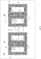
- One embodiment of the multi-layer printed circuit board comprises a first through going aperture and a second through going aperture. The common straight leg of the first magnetically permeable core is projecting through the first through going aperture and the common straight leg of the second magnetically permeable core is projecting through the second through going aperture.
- a first board wiring pattern is arranged around the first through going aperture and comprises at least one of the first input inductor winding, the first half-winding of the first output inductor winding and the first half-winding of the second output inductor winding.
- a second board wiring pattern is arranged around the second through going aperture and comprises at least one of the second input inductor winding, the second half-winding of the first output inductor winding and the second half-winding of the second output inductor winding.
- the multi-layer printed circuit board may comprise one or more additional through going apertures to accommodate additional legs of the first and second magnetically permeable cores, e.g. four additional legs for a pair E-shaped magnetically permeable cores.
- integrated magnetics transformer assembly comprise conventional wire type and wire material such as solid copper wire or litz wire for each of the first and second input inductor windings and each of first and second output inductor windings. Further embodiments of the integrated magnetics transformer assembly may use a combination of the above-mentioned PCB based wiring and the conventional types of wires.
- each of the first and second magnetically permeable cores may possess the conventional transformer core geometry such as E-shaped, toroid shaped, rectangular etc.
- the first core may comprise a first substantially rectangular core portion formed by mechanical coupling of three substantially straight legs and the common straight leg and the second core comprises a second substantially rectangular core portion formed by mechanical coupling of three substantially straight legs and the common straight leg.
- the integrated magnetics transformer assembly comprises first and second magnetically permeable E-shaped cores wherein each of the E-shaped cores comprises the common leg arranged in-between a pair adjacent outer legs.
- the advantageous configuration of the second half-winding of the first output inductor winding and the second half-winding of the second output inductor winding where these half windings produce oppositely directed magnetic fluxes can be achieved by different half-winding arrangements on the second core depending on the chosen core geometry.
- the first half-winding of the first output inductor winding and the first half-winding of the second output inductor winding are wound around a common straight leg of the first core; and the second half-winding of the first output inductor winding and the second half-winding of the second output inductor winding are wound around a common straight leg of the second core.
- the first half-winding of the first output inductor winding and the first half-winding of the second output inductor winding are connected in same direction and the second half-winding of the first output inductor winding and the second half-winding of the second output inductor winding are connected in reverse direction.
- the first half-winding of the first output inductor winding and the first half-winding of the second output inductor winding produce magnetic fluxes in the same direction through the common leg of the first core while the second half-winding of the first output inductor winding and the second half-winding of the second output inductor winding produce magnetic fluxes in the opposite direction through the common leg of the second core.
- the magnetic fluxes in the second core generated by the second half-windings are preferably oppositely directed not only through the common leg of the second core, but at all points throughout the second substantially closed magnetic flux path.
- the magnetic fluxes in the first core generated by the first half-windings are preferably flowing in the same direction at all points throughout the second substantially closed magnetic flux path.
- the first input inductor winding is preferably configured or oriented such that it produces magnetic flux in the same direction as the first half-windings.
- the second input inductor winding is preferably configured or oriented such that it produces magnetic flux in the same direction as the second half-winding of the first output inductor winding and therefore in opposite direction to the magnetic flux produced by the second half-winding of the second output inductor winding.
- the first input inductor winding is preferably wound around the common straight leg of the first magnetically permeable core and the second input inductor winding is preferably wound around the common straight leg of the second magnetically permeable core.
- the first input inductor winding, the first half-winding of the first output inductor winding and the first half-winding of the second output inductor winding are arranged adjacently on the common straight leg of the first core.
- the second input inductor winding, the second half-winding of the first output inductor winding and the second half-winding of the second output inductor winding are arranged adjacently on the common straight leg of the second magnetically permeable core.
- input and output inductor windings arranged on a common leg of the first core may partially or fully overlap i.e. being partially or fully interleaved such that the first and second segments of the first core partly or fully overlap.
- the first and second half-windings of the first output inductor winding comprises the same number of turns and the first and second half-windings of the second output inductor winding comprises the same number of turns.
- the number of windings of the first and second half-windings of the first output inductor winding may differ in alternative embodiments and the number of windings of the first and second half-windings of the second output inductor winding may differ as well.
- the number of turns of the second half-windings of the first and second output inductor windings is preferably identical to facilitate to good magnetic flux cancellation in the second core.
- a second aspect of the present invention relates to a multiple-input isolated power converter comprising an integrated magnetics transformer assembly according to any of the above-described embodiments thereof.
- the multiple-input isolated power converter comprises a first input terminal connectable to a first DC or AC input voltage source.
- a first input driver is operatively coupled to the first DC or AC input voltage and the first input inductor winding to supply a first drive signal thereto.
- the multiple-input isolated power converter further comprises a second input terminal connectable to the first DC or AC input voltage or a second DC or AC input voltage source.
- a second input driver is operatively coupled to the first or second DC or AC input voltage and the second input inductor winding to supply a second drive signal thereto.
- a first rectifier or a first inverter element is operatively coupled between a first converter output and a pair of winding terminations of the series coupled first and second half-windings of the first output inductor winding and a second rectifier or a second inverter element is operatively coupled between a second converter output and a pair of winding terminations of the series connected first and second half-windings of the second output inductor winding.
- the present multiple-input isolated power converter may be embodied in a wide range of useful DC-DC or DC-AC power converter topologies.
- the DC-DC isolated power converter topologies include the first and second rectifiers to rectify the first and second AC voltages supplied across the respective pairs of winding terminations of the series coupled first and second half-windings of the first and second output inductor windings.
- Each of the first and second rectifiers may include a semiconductor diode or a semiconductor diode bridge or a transistor switch based synchronous rectifier.
- the DC-DC isolated power converter topologies comprises DC-DC isolated boost converters, DC-DC isolated buck converters, DC-DC dual active bridge (DAB) converters, isolated two inductor one capacitor (LLC) resonant DC-DC power converters etc. as explained in additional detail below in connection with the appended figures.
- the first and second converter outputs may be separate voltage nodes providing two independent or separate rectified DC output voltages of the multiple-input isolated DC-DC power converter. In other useful embodiments, the first and second converter outputs are coupled to a common output node to provide a single rectified DC output voltage of the power converter.
- the DC-AC isolated power converter topologies comprise the first and second inverter elements to convey, and possibly filter, the first and second AC voltages, generated across the respective pairs of winding terminations of the series coupled first and second half-windings, before application to the first and second converter outputs as respective AC output voltages of the DC-AC isolated power converter.
- the first and second inverter elements may for example comprise respective smoothing inductors.
- the designations 'input' of the first and second input inductor windings and the designations 'output' of the first and second output inductor windings are all arbitrary and may be interchanged depending on how the integrated magnetics transformer assembly is electrically interconnected or coupled in a specific isolated power converter design. This feature is an inherent consequence of the reciprocal nature of all transformer functions.
- the first and second output inductor windings are operatively connected to respective inputs of a primary side of the power converter while the first and second input inductor windings are operatively coupled to a common or separate outputs of a secondary side of the power converter.
- the multiple-input isolated power converter comprises an integrated magnetics transformer assembly according to any of the above-described embodiments thereof.
- the first input terminal of the multiple-input isolated power converter is connectable to a first DC or AC input voltage and the first input driver is operatively coupled to the first DC or AC input voltage and to the pair of winding terminations of the series coupled first and second half-windings of the first output inductor winding to supply a first drive signal thereto.
- the second input terminal is connectable to the first or the second DC or AC input voltage and the second input driver is operatively coupled to the first or the second DC or AC input voltage and the pair of winding terminations of the series connected first and second half-windings of the second output inductor winding to supply a second drive signal thereto.
- the first rectifier, or the first inverter element is operatively coupled between the first converter output and the first input inductor winding and the second rectifier, or the second inverter element, is operatively coupled between the second converter output and the second input inductor winding.
- Boost topologies of the multiple-input isolated power converter may comprise a first boost inductor coupled between the first DC or AC input voltage and the first input driver and a second boost inductor coupled between the second DC or AC input voltage and the second input driver.
- Buck topologies of the multiple-input isolated power converter may comprise first and second separate buck inductors coupled between outputs of the first and second rectifiers, respectively, and a common or shared converter output.
- a particular advantageous buck implementation of the present multiple-input isolated power converter comprises a single or first buck inductor coupled in-between the common converter output and a common node of the outputs of the first and second rectifiers. The ability of certain buck topologies of the present multiple-input isolated power converter to share a common buck inductor is a unique advantage.
- Each of the first and second input drivers may comprise well-known driver topologies such as a half-bridge driver or an H-bridge driver configured for applying the drive signal across the first or second input inductor winding.
- the first input driver comprises a first H-bridge having a pair of complementary outputs connected to respective winding terminations of the first input inductor winding.
- the second input driver comprises a second H-bridge having a pair of complementary outputs connected to respective winding terminations of the second input inductor winding.
- the first and second drive signals, applied to the first and second input inductor windings, respectively, preferably comprise respective PWM modulated drive signals.
- Duty cycles of the first and second PWM modulated drive signals may be adjusted to provide converter output voltage control or regulation by a suitable feedback control loop of the multiple-input isolated power converter.
- Each input driver may comprise a single or a plurality of appropriately arranged semiconductor switches such as IGBT switches or MOSFET switches to form the well-known driver topologies.
- each of the first and rectifiers may comprise a plurality of rectifying elements such as semiconductor diodes for example two semiconductor diodes configured as a half-wave rectifier or four semiconductor diodes configured as a full-wave rectifier.
- each of the first and rectifiers may comprise a plurality of transistor switches, e.g. MOS-FETs, configured as respective active diodes to enable synchronous rectification and support reverse power transfer.
- the first and second converter outputs may be configured in different ways.
- the first and second converter outputs are combined to form a common output node producing a single DC output voltage of the multiple-input isolated power converter.
- One or several output capacitor(s) may be coupled to the common output node to suppress ripple voltages in the DC output voltage produced by respective rectified voltage waveforms at the outputs of the first and second rectifiers.
- the DC output voltage is produced by a combination of voltage or power contributions from the first and second rectifiers.
- An alternative embodiment of the multiple-input isolated power converter is configured to produce separate first and second DC output voltages, or first and second separate AC output voltages, at separate output voltage terminals.
- the same isolated power converter can be readily adapted to fit a variety of different power converter or inverter applications and therefore reduce the number of variants required of a particular power converter topology.
- the present isolated power converter is capable of lowering assembly costs, component costs, stock costs etc.
- the flexibility offered by the present multiple-input isolated power converter is particularly well-suited for power conversion in connection with clean energy sources like photovoltaic cells which often generate a wide range of different input voltages for power converters.
- the present integrated magnetics transformer assembly also may be integrated in numerous other well-known DC-DC isolated power converter topologies such as flyback topologies, forward topologies, push-pull topologies, SEPIC topologies, current doubler rectifier topologies etc.
- FIG. 1A shows a schematic drawing of a prior art dual-input isolated boost DC-DC power converter comprising two fully parallel converters and a common converter output.
- the power converter comprises two converter stages, build around transformer T1 and transformer T2, respectively, and operating fully in parallel with a common output capacitor C.
- the two transformers T1 and T2 are fully separate.
- the input inductor winding or primary winding of T1 is driven by a first H-bridge driver comprising MOSFET switches M1-M4 while the input inductor winding of T2 is driven by a second, separate, H-bridge driver comprising MOSFET switches M5-M8.
- This prior art power converter possesses a boost-type structure or topology with a common output DC output across output capacitor C such that only one converter stage at a time is allowed to transfer energy from either of the DC input voltage sources V 1 and V 2 to the load R L . Otherwise, the other converter stage stops working because the H-bridge rectifier of the other converter stage is blocked if there is any duty cycle mismatch, phase mismatch or input voltage mismatch between inputs of the two converter stages. Even though this problem can be addressed with input current control, similar and even more difficult problems arise in buck topology multiple-input power converters.
- the two DC voltage transfer functions are independent and such that the DC output voltage V 0 of the power converter is only determined by a single input voltage source and its corresponding duty cycle.
- FIG.1B is a schematic drawing of another prior art dual-input isolated boost DC-DC power converter comprising two fully parallel converter stages build around transformer T1 and transformer T2, respectively, and a common converter output.
- the secondary windings S1 and S2 of transformer T1 and T2 are arranged in series and connected to a single shared full-wave rectifier comprising diodes D1-D4.
- the output of the rectifier is coupled to a single output capacitor C.
- This power converter topology allows the two converter stages to transfer energy from input sources V 1 and V 2 to the load R L within a certain range of phase shift between PWM modulated drive signals at the expense of an undesired and relatively large circulating current in the second H-bridge input driver (MOSFETs M5-M7) and primary side of the transformer T2 when the transformer T1 is active.
- the circulating current leads to substantial power losses in this prior art DC-DC power converter.
- the range of multiple-input isolated power converters disclosed below in accordance with various exemplary embodiments of the present invention is based on a novel integrated magnetics transformer assembly 200 depicted on FIG. 2 .
- the present range of multiple-input isolated power converters eliminates the operational limitations and disadvantages of the above-mentioned prior art dual-input isolated boost DC-DC power converters.
- FIG. 2 is a schematic drawing of an integrated magnetics transformer assembly 200, or discrete transformer assembly, in accordance with a preferred embodiment of the invention.
- the integrated magnetics transformer assembly comprises a first magnetically permeable core 202 and a second and separate magnetically permeable core 210.
- the first magnetically permeable core 202 is an E-shaped core which comprises a substantially straight center leg 203 arranged in-between a pair adjacent outer legs 207, 205.
- First and second parallel and substantially closed magnetic flux paths ⁇ 1 extend through the center leg 203 and the first and second outer legs 207, 205, respectively, when input current flows through a first input inductor winding P1.
- the second magnetically permeable core 210 is also E-shaped and may have substantially the same dimensions and magnetic properties as the first magnetically permeable core 202.
- the second magnetically permeable core 210 comprises a substantially straight center leg 211 arranged in-between a pair adjacent outer legs 215, 213.
- First and second parallel and substantially closed magnetic flux paths ⁇ 2 extend through the center leg 211 and the first and second outer legs 215, 213, respectively, when input current flows through a second input inductor winding P2.
- each of the first and second magnetically permeable cores may possess various other shapes than the E-shaped form of the present embodiment - for example a toroid shape, a rectangular shape etc.
- Each of the first and second magnetically permeable cores 202, 210 preferably comprises a material possessing high magnetic permeability such as a soft magnetic material like Ferrite or a ferromagnetic alloy like Sheet steel, Silicon steel, Cast steel, Tungsten steel Magnet steel, cast iron, Nickel etc.
- a soft magnetic material like Ferrite or a ferromagnetic alloy like Sheet steel, Silicon steel, Cast steel, Tungsten steel Magnet steel, cast iron, Nickel etc.
- the first input inductor winding P1 is wound around a first predetermined segment of the straight center leg 203 of the first magnetically permeable core or first core 202 and a second input inductor winding P2 is wound around a first predetermined segment of the straight common center leg 211 of the second magnetically permeable core or second core 210.
- the integrated magnetics transformer assembly 200 further comprises a first output inductor winding comprising series coupled first and second half-windings S1, S3, respectively.
- the first half-winding S1 is wound around the center leg 203 of the first core 202 and arranged adjacently to the first input inductor winding P1.
- the second half-winding S3 is wound around the common center leg 211 of the second core 210 and arranged adjacently to the second input inductor winding P2.
- a second output inductor winding of integrated magnetics transformer assembly 200 comprises series or cascade coupled first and second half-windings S2, S4, respectively.
- the first half-winding S2 is wound around the common center leg 203 of the first core 202 and arranged adjacently to the first input inductor winding P1.
- the second half-winding S4 is wound around the common center leg 211 of the second core 210 and arranged adjacently to the second half-winding S3 of the first output inductor winding.
- the directions of the magnetic flux running through the center leg 203 and the outer legs 205, 207 of the first core 202 are indicated by the respective flux arrows on the broken line indicating closed magnetic flux paths ⁇ 1.
- the depicted direction of the magnetic flux through the center leg 203 follows from the well-known right-hand rule for current flowing into winding termination A of the first input inductor winding P1 and out of winding termination B.
- Each of the first half-winding S1 of the first output inductor winding and the first half-winding S2 of the second output inductor winding is wound in the same direction as P1 around the common center leg 203.
- the second half-winding S4 of the second output inductor winding has a reversed connection or winding orientation relative to the series connected first half-winding S2 as illustrated on the drawing such that current flowing into winding termination G, through the series connected half-windings S2 and S4 and out of winding termination H on S4 leads to an opposite current direction in S4 relative to the current direction in S2.
- the magnetic flux induced by the current flow in half-winding S4 through the common center leg 211 flows in opposite direction to the magnetic flux induced by the current flow in half-winding S3 and the second input inductor winding P2 through the common center leg 211.
- the same oppositely directed magnetic fluxes ⁇ 4 generated by half-winding S4 extends through the entire closed flux paths ⁇ 2.
- the magnetic flux cancellation in the common center leg 211 can be either partial or substantially complete if the half-windings S3 and S4 are substantially identical, i.e. possessing the same number of windings.
- the second half-winding S3 of the first output inductor winding and the second half-winding S4 of the second output inductor winding are configured or oriented to produce oppositely directed magnetic fluxes through the closed magnetic flux paths ⁇ 4 and ⁇ 2 of the second core 210.
- the first half-winding S1 of the first output inductor winding and the first half-winding S2 of the second output inductor winding are configured to produce aligned, i.e. in the same direction, magnetic fluxes through the first substantially closed magnetic flux paths ⁇ 1.
- the cancellation of magnetic flux in the common center leg 211 of the second core 210 has been achieved by the reversed winding arrangement of the second half-winding S4 leading to a reversal of the direction of the magnetic flux.
- the second input inductor winding may be arranged on the center leg 211 while one or both of the first and second half-windings of the output inductor winding may be arranged on one of the outer legs in other embodiments of the invention.
- the second half-winding S4 is moved to the second outer leg 213 while the residual inductor windings are maintained as illustrated on FIG. 2 .
- the second half-winding S4 is now arranged with the same winding orientation as the first half-winding S2 which leads to the generation of oppositely directed magnetic flux through the closed magnetic flux paths ⁇ 4 by the second half-winding S4 relative to the magnetic flux generated by second half-winding S3 through the closed magnetic flux paths ⁇ 2.
- magnetic flux cancellation is also achieved by this alternative placement and orientation of the second half-winding S4 on the second core 210.
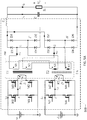
- FIG. 3 is a schematic drawing of a dual-input single output isolated boost DC-DC power converter 300 comprising an integrated magnetics transformer assembly 200 in accordance with the above-described preferred embodiments thereof.
- the integrated magnetics transformer assembly 200 has been depicted by its electrical equivalent of the mechanical transformer structure depicted on FIG. 2 above. Be kind to the notice the previous naming convention of the various input and output inductor windings of the first and second cores 202, 210, respectively, has been maintained to facilitate cross-reference.
- the turns ratio is 1: n as indicated on the figure where n may have a value between 0.1 to 100 such as between 2 and 16.
- the turns ratio being defined as the number of input inductor windings of each of the first and second input or primary side inductor windings P1 and P2 relative to the total number of windings on the series coupled first and second half-windings S1 and S3, or S2 and S4, of the respective output inductor windings.
- the dual-input single output isolated boost DC-DC power converter 300 or DC-DC power converter 300 comprises a first and second independently operating converter sections or stages.
- the first converter section comprises a first input driver, comprising a MOS-FET based H-bridge M1-M4, electrically coupled to the first input inductor winding P1 through the pair of winding terminations or terminals A, B.
- the input side of the first input driver is coupled to a boost inductor L 1 arranged in series with an input voltage or power source V 1 schematically depicted as an ideal voltage source.
- the first H-bridge driver is configured to supply a first drive signal to the first input inductor winding P1 for example comprising a first PWM modulated drive signal.
- the DC-DC power converter 300 comprises furthermore a second input driver, likewise comprising a second MOS-FET based H-bridge comprising M5-M8, electrically coupled to the second input inductor winding P2 through the pair of winding terminations or terminals C, D.
- the input of the second input driver is coupled to a second boost inductor L 2 arranged in series with the second input voltage or power source V 2 schematically depicted as an ideal voltage source.
- the second H-bridge is configured to supply a second drive signal to the second input inductor winding P2 for example comprising a second PWM modulated drive signal.
- the duty cycle of each of the PWM modulated first and second drive signals may be selectively adjusted to control a rectified DC output voltage V 0 in conventional ways such as through a feedback control loop.
- the DC voltage of the input voltage source V 1 may vary considerably depending on its type and specific characteristics.
- the DC voltage may for example have a value between 5 V and 100 V and the same applies for the DC voltage of the second input voltage source V 2 .
- Terminations E, F of the first output inductor winding comprising series coupled first and second half-windings S1, S3, respectively, are electrically coupled to a first full-bridge output rectifier build around semiconductor diodes D1-D4.
- input voltage and power supplied by the first converter stage around core 202 is transferred to the rectified DC output voltage V 0 applied by an output of the first full-bridge output rectifier across output capacitor C and parallel load resistor R L .
- the terminations G, H of the second output inductor winding comprising series coupled first and second half-windings S2, S4, respectively, are electrically coupled to a second full-bridge output rectifier build around semiconductor diodes D5-D8.
- the output of the second full-bridge output rectifier is coupled to the output for the first full-bridge rectifier in parallel.
- input voltage and power supplied by the second converter stage around core 210 is transferred to a rectified DC output voltage V 0 across output capacitor C and parallel load resistor R L .
- the previously discussed decoupling of the two primary or input inductor windings P1, P2 provided by the present integrated magnetics transformer assembly 200 eliminates the power coupling effects and the circulating currents discussed above in connection with the prior art DC-DC converters depicted on Figs. 1A and 1B .
- the decoupling mechanism is schematically illustrated by the indicated reverse direction of current flow in the second half-winding S4 of the second output inductor winding and the second half-winding S3 of the first output inductor winding.
- the magnetic fluxes induced by these winding currents are oppositely directed and cancel through the common center leg as explained above. Consequently, the voltage reflected back to the input inductor winding P2 of the second core 210 by the resulting magnetic flux from the currents flowing in the half-windings S3 and S4 on the secondary or output side of the second core 210 is eliminated such that the above-discussed generation of circulating currents around the input inductor winding P2 and its associated input driver is eliminated.
- This voltage transfer function is valid for zero phase difference or shift between the PWM drive signals applied to the first and second input inductor windings P1 and P2.
- the voltage transfer function of the present DC-DC power converter 300 leads to a very wide input voltage range and a wide output voltage range such that varying application specific constraints on minimum and maximum DC input voltage and/or DC output voltages can be met.
- several transformer design parameters notably the turns ratios n 1 and n 2 , are available for the designer of the power converter. Hence, the power converter designer is left with considerable flexibility in customizing performance metrics of the power converter, including input and output voltage ranges, allowing a specific power converter design to operate efficiently in a wide range of applications.
- the DC output voltage V 0 is adjustable by controlling the phase difference (interleaving) between the PWM drive signals applied to the first and second input inductor windings P1 and P2. This provides a distinct flexibility advantage in connection with designing control scheme and devices for D C output voltage control. If the duty cycle is kept constant and phase shift control exploited to regulate the DC output voltage V 0 , the maximum DC output voltage is achieved when the phase shift is 0° or 180°. The minimum DC output voltage V0 is achieved when the phase-shift is 90°.
- the two DC input voltage sources are both PV sources.
- MPPT maximum power point tracking
- the power converter output is connected to a constant DC bus at a desired DC voltage for example 150V.
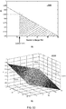
- the input voltage range for each of the DC input voltage sources V 1 and V 2 is shown on the graph 1000 of FIG. 10A . None of the first and second DC input voltages can drop below the indicated lower limit at 11.3 V as indicated on the x-axis of graph 1000.
- the maximum allowable duty cycle D is set to an exemplary value of 85%.
- the surface 1013 of the graph 1010 of FIG. 10B depicts the 3D relationship between the common duty cycle, D, of the PWM drive signals (vertical axis) and DC voltages V1 and V2 (x-axis and y-axis) provided by the first and second DC input voltage sources, respectively, for a fixed DC output voltage of 150 V.
- the present DC-DC power converter 300 is suitable for diversity power sources for example a pair of solar panels which may be exposed to different environmental conditions at the same time (for example: one solar panel is hidden by a shadow of a tree or a building while the other solar panel is exposed to direct sunlight; or one solar panel is facing east while the other solar panel is facing west).
- These energy source characteristics with differing input voltages between several input voltage/energy sources and varying voltage level over time are often found in renewable energy applications.
- the present DC-DC power converter 300 is particularly well-adapted to make an efficient interface to these types of input energy sources due to the wide input voltage range and wide converter output voltage range of the converter 300.
- FIG. 4 shows a plurality of graphs 405- 450 depicting respective input, winding and output voltage waveforms of the dual-input isolated boost DC-DC converter 300 of FIG. 3 .
- Phases 1-4 of the current and voltage waveforms are indicated at lowermost portion of the graph by the vertical dotted lines and corresponding time symbols t 0 , t 1 , t 2 , t 3 , t 4 .
- the depicted voltage and current waveforms represent a 90 degrees phase angle shift between the first and second PWM drive signals to the first and second input inductor windings P1 and P2, respectively.
- the first and second converter stages, around transformers T1 and T2, respectively, of the dual-input isolated boost DC-DC converter 300 operate with a phase shift of 90 degrees.
- the upper graphs 405, 410 show the respective PWM waveforms of MOSFET switch drive signals S 1,2 and S 3,4 of the MOSFET switches M1-M4 of the first H-bridge input driver.
- the following graphs 415, 420 show respective PWM waveforms of MOSFET switch drive signals S 5,6 and S 7,8 of the MOSFET switches M5-M8 of the second H-bridge input driver
- Graph 425 shows the waveform of the first PWM drive signal V A,B that is applied to the first input or primary side inductor winding P1. This waveform has a period time T and a switching duty cycle of 75%. As indicated, the graph 430 shows the 90 degrees phase shifted waveform of the second PWM drive signal V C,D applied to the second input or primary side inductor winding P2. This signal has the same period time T and the same switching duty cycle of about 75% as the first drive signal.
- Graphs 435, 440 show the respective corresponding current waveform of winding currents in P1 and P2. It is evident that each of the first and second boost inductors L 1 and L 1 are charged in phases 2 and 4 and discharged into their respective primary side inductor windings P1, P2 in phases 1 and 3 albeit with reversed polarity.
- Graph 445 depicts the voltage waveform V EF induced across the terminations E, F of the first output inductor winding, comprising series coupled first and second half-windings S1, S3, respectively.
- Graph 450 depicts the voltage waveform V GH induced across the terminations G, H of the second output inductor winding, comprising series coupled first and second half-windings S2, S4, respectively.
- the 90 degrees phase shift between the first and second PWM input drive signals is clearly reflected in the voltage waveforms V EF and V GH of the secondary or output transformer windings.
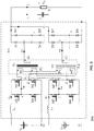
- FIG. 5A is a schematic drawing of a dual-input single output isolated buck DC-DC power converter 500 comprising an integrated magnetics transformer assembly 200 in accordance with the above-described preferred embodiments thereof.
- the application of the integrated magnetics transformer assembly 200 in the present buck DC-DC power converter provides a unique possibility for sharing the output or buck inductor L 1 and output capacitor C.
- the buck DC-DC power converter achieves an important reduction of the number of external components compared to prior art dual-input buck type DC-DC power converters.
- FIG. 5B is a schematic drawing of another embodiment of a dual-input single output isolated buck DC-DC power converter 550 comprising an integrated magnetics transformer assembly 200 in accordance with the above-described preferred embodiments thereof.
- the present embodiment comprises separate first and second output/buck inductor L 1 and L 2 coupled between respective ones of the first and second rectifier outputs and the common DC output of the DC-DC power converter 550.
- FIG. 6 is a schematic drawing of a dual-input dual active bridge (DAB) topology DC-DC power converter 600 comprising an integrated magnetics transformer assembly 200 in accordance with the above-described preferred embodiments thereof.
- a first active full-wave rectifier is formed around MOS-FETs S1-S4 and a second active full-wave rectifier is formed around MOS-FETs S5-S8.
- FIG. 7 is a schematic drawing of a dual-input isolated two inductor (L I1 and L I2 ) and capacitor (C 1 and C 2 ) (LLC) topology DC-DC power converter 700 comprising the integrated magnetics transformer assembly 200 in accordance with the above-mentioned preferred embodiments thereof.
- FIG. 8 is a schematic drawing of a dual-input boost DC-DC power converter 800 with side-shifted windings comprising the integrated magnetics transformer assembly 200 in accordance with the above-mentioned preferred embodiment thereof.
- the terminations of the series coupled first and second half-windings S1 and S3, of the first output inductor winding are coupled to the input side of the DC-DC power converter more specifically to the complementary outputs of the first input H-bridge driver.
- the terminations of the series coupled first and second half-windings S2 and S4 of the second output inductor winding are also coupled to the input side of the DC-DC power converter - more specifically to the complementary outputs of the second H-bridge driver.
- the letter references of these half-windings have been changed from 'S' to 'P'.
- the first and second input or primary side inductor windings P1 and P2 are now arranged at the output side of the DC-DC power converter 800 - more specifically coupled to the respective first and second full-bridge rectifiers.
- the letter references of these input inductor windings have been changed from 'P' to 'S'.
- the present dual-input boost DC-DC power converter 800 may possess substantially the same power converter characteristics as the earlier discussed dual-input boost DC-DC power converter embodiment 300 of FIG. 3 by simply reversing the turns ratio n of each of the transformers T1 and T2 of the integrated magnetics transformer assembly 200.
- the designations 'input' of the first and second input inductor windings P1 and P2 and the term 'output' of the first and second output inductor windings are all arbitrary and may be interchanged depending on how the integrated magnetics transformer assembly 200 is coupled in a specific DC-DC power converter design.
- FIG. 9 is a schematic drawing of a dual-input and dual-output isolated boost DC-DC power converter 900 comprising an integrated magnetics transformer assembly 200 in accordance with the above-mentioned preferred embodiments thereof.
- the present boost DC-DC power converter 900 comprises two separate converter DC output voltages V 01 and V 02 provided across two separate output capacitors C 1 and C 2 .
- the earlier discussed isolated boost DC-DC power converter 300 is configured to produce a single converter output having a common DC output voltage.
- the inventive integrated magnetics transformer assembly 200 can also be used in multiple-input and dual outputs power converter topologies.
- the first DC output voltage V 01 is generated by a first full-wave rectifier comprising diodes D1-D4 having respective inputs coupled to winding terminations E, F of the first half-winding S1 and the second half-winding S3 of the first output inductor winding.
- the second DC output voltage V 02 is generated by a second full-wave rectifier comprising diodes D5-D8 having respective inputs coupled to winding terminations G, H of the first half-winding S2 and the second half-winding S4 of the second output inductor winding.
- the DC-DC power converter may cease to function.
- the present dual-input and dual-output isolated boost DC-DC power converter 900 renders the two separate converter DC output voltages V 01 and V 02 completely independent.
- the DC output voltages V 01 and V 02 are uncoupled even though multiple transformer windings are used on the first and second transformers T1 and T2.
- Another advantage is that the respective converter loads, schematically illustrated by first and second load resistors R L1 and R L2 are capable of sharing the total energy delivered by both input voltage or energy sources V 1 and V 2 .
- the distribution of output power between the first and second load resistors load resistors R L1 and R L2 at the first and second converter outputs can be controlled by shifting the phase (interleaving) of the previously discussed PWM drive signals applied to the first and second input inductor windings P1 and P2, respectively, of the first and second transformers T1 and T2. For example, when the phase shift between the PWM input drive signals is zero, the full output power is delivered to the first load resistor R L1 while zero output power is delivered to the second load resistor R L2 . If the phase shift between the PWM drive signals is adjusted to 90 degrees, the output power is split equally between the first load resistor R L1 and the second load resistor R L2 .
- phase shift between the PWM input drive signals is set to 180 degrees, the full output power is delivered to the second load resistor R L2 while zero output power is delivered to the first load resistor R L1 .
- Any other desired power distribution between the first and second converter loads can be obtained by an appropriate setting of the phase shift between the PWM input drive signals.
Landscapes
- Engineering & Computer Science (AREA)
- Power Engineering (AREA)
- Dc-Dc Converters (AREA)
- Coils Of Transformers For General Uses (AREA)
Claims (15)
- Ensemble transformateur d'éléments magnétiques intégrés (200), comprenant :- un premier noyau magnétiquement perméable (202) formant un premier trajet de flux magnétique sensiblement fermé (φ1),- un second noyau magnétiquement perméable (210) formant un second trajet de flux magnétique sensiblement fermé (φ2),- un premier enroulement de bobine d'induction d'entrée (P1) enroulé autour d'un premier segment prédéterminé (203) du premier noyau magnétiquement perméable (202) et un second enroulement de bobine d'induction d'entrée (P2) enroulé autour d'un premier segment prédéterminé (211) du second noyau magnétiquement perméable (210),- un premier enroulement de bobine d'induction de sortie comprenant des premier et second demi-enroulements couplés en série (S1, S3) dans lequel le premier demi-enroulement (S1) est enroulé autour d'un deuxième segment prédéterminé du premier noyau magnétiquement perméable (202) et le second demi-enroulement (S3) est enroulé autour d'un deuxième segment prédéterminé du second noyau magnétiquement perméable (210),- un second enroulement de bobine d'induction de sortie comprenant des premier et second demi-enroulements couplés en série (S2, S4) dans lequel le premier demi-enroulement (S2) est enroulé autour d'un troisième segment prédéterminé du premier noyau magnétiquement perméable (202) et le second demi-enroulement (S4) est enroulé autour d'un troisième segment prédéterminé du second noyau magnétiquement perméable (210) ;dans lequel le premier noyau (202) conjointement avec le premier enroulement de bobine d'induction d'entrée (P1), le premier demi-enroulement (S1) du premier enroulement de bobine d'induction de sortie et le premier demi-enroulement (S2) du second enroulement de bobine d'induction de sortie, forme le premier transformateur (T1), et le second noyau (210) conjointement avec le second enroulement de bobine d'induction d'entrée (P2), le second demi-enroulement (S3) du premier enroulement de bobine d'induction de sortie et le second demi-enroulement (S4) du second enroulement de bobine d'induction de sortie, forme le second transformateur (T2) ;
dans lequel le second demi-enroulement (S3) du premier enroulement de bobine d'induction de sortie et le second demi-enroulement (S4) du second enroulement de bobine d'induction de sortie sont configurés pour produire des flux magnétiques dirigés de manière opposée à travers le second trajet de flux magnétique sensiblement fermé (φ2) ; et
le premier demi-enroulement (S1) du premier enroulement de bobine d'induction de sortie et le premier demi-enroulement (S2) du second enroulement de bobine d'induction de sortie sont configurés pour produire des flux magnétiques alignés à travers le premier trajet de flux magnétique sensiblement fermé (φ1). - Ensemble transformateur d'éléments magnétiques intégrés (200) selon la revendication 1, dans lequel le premier demi-enroulement (S1) du premier enroulement de bobine d'induction de sortie et le premier demi-enroulement (S2) du second enroulement de bobine d'induction de sortie sont enroulés autour d'une patte rectiligne commune (203) du premier noyau magnétiquement perméable (202) ; et
le second demi-enroulement (S3) du premier enroulement de bobine d'induction de sortie et le second demi-enroulement du second enroulement de bobine d'induction de sortie sont enroulés autour d'une patte rectiligne commune (211) du second noyau magnétiquement perméable (210) ; dans lequel
le premier demi-enroulement (S1) du premier enroulement de bobine d'induction de sortie et le premier demi-enroulement (S2) du second enroulement de bobine d'induction de sortie sont connectés dans la même direction
et le second demi-enroulement (S3) du premier enroulement de bobine d'induction de sortie et le second demi-enroulement (S4) du second enroulement de bobine d'induction de sortie sont connectés dans une direction inverse. - Ensemble transformateur d'éléments magnétiques intégrés (200) selon la revendication 2, dans lequel le premier enroulement de bobine d'induction d'entrée (P1) est enroulé autour de la patte rectiligne commune (203) du premier noyau magnétiquement perméable (202) ; et
le second enroulement de bobine d'induction d'entrée est enroulé autour de la patte rectiligne commune (211) du second noyau magnétiquement perméable (210). - Ensemble transformateur d'éléments magnétiques intégrés (200) selon la revendication (3), dans lequel :- le premier enroulement de bobine d'induction d'entrée (P1), le premier demi-enroulement du premier enroulement de bobine d'induction de sortie et le premier demi-enroulement du second enroulement de bobine d'induction de sortie sont agencés de manière adjacente sur la patte rectiligne commune (203) du premier noyau magnétiquement perméable (202) ; et- le second enroulement de bobine d'induction d'entrée (P2), le second demi-enroulement du premier enroulement de bobine d'induction de sortie et le second demi-enroulement du second enroulement de bobine d'induction de sortie sont agencés de manière adjacente sur la patte rectiligne commune (211) du second noyau magnétiquement perméable (210).
- Ensemble transformateur d'éléments magnétiques intégrés (200) selon une quelconque revendication 2 à 4, dans lequel :- le premier noyau magnétiquement perméable (202) comprend une première partie de noyau sensiblement rectangulaire formée par liaison mécanique de trois pattes sensiblement rectilignes (203, 205, 207) et de la patte rectiligne commune ; et- le second noyau magnétiquement perméable (210) comprend une seconde partie de noyau sensiblement rectangulaire formée par accouplement mécanique de trois pattes sensiblement rectilignes (211, 213, 215) et de la patte rectiligne commune.
- Ensemble transformateur d'éléments magnétiques intégrés (200) selon la revendication 5, comprenant des premier et second noyaux magnétiquement perméables en forme de E (202, 210) dont chacun comprend la patte commune (203, 211) agencée entre une paire de pattes externes adjacentes (205, 207, 213, 215).
- Ensemble transformateur d'éléments magnétiques intégrés (200) selon l'une quelconque des revendications précédentes, comprenant un élément de retenue fixé aux premier et second noyaux magnétiquement perméables (202, 210) de sorte à fixer ceux-ci dans une relation spatiale prédéterminée.
- Ensemble transformateur d'éléments magnétiques intégrés (200) selon la revendication 7, dans lequel l'élément de retenue comprend une carte de circuit imprimé.
- Ensemble transformateur d'éléments magnétiques intégrés (200) selon les revendications 4 et 8, comprenant une carte de circuit imprimé multicouches possédant une première ouverture traversante et une seconde ouverture traversante ;
la patte rectiligne commune (203) du premier noyau magnétiquement perméable (202) faisant saillie à travers la première ouverture traversante et la patte rectiligne commune (211) du second noyau magnétiquement perméable (210) faisant saillie à travers la seconde ouverture traversante ; et
un premier tracé de câblage de carte agencé autour de la première ouverture traversante et comprenant au moins l'un d'entre le premier enroulement de bobine d'induction d'entrée (P1), le premier demi-enroulement du premier enroulement de sortie de bobine d'induction et le premier demi-enroulement (S2) du second enroulement de bobine d'induction de sortie ; et
un second tracé de câblage de carte agencé autour de la seconde ouverture traversante et comprenant au moins l'un d'entre le second enroulement de bobine d'induction d'entrée (P2), le second demi-enroulement du premier enroulement de bobine d'induction de sortie et le second demi-enroulement du second enroulement de bobine d'induction de sortie. - Ensemble transformateur d'éléments magnétiques intégrés (200) selon l'une quelconque des revendications 7 à 9, dans lequel les premier et second noyaux magnétiquement perméables (202, 210) sont séparés par une distance d'au moins 6 mm par l'élément de retenue.
- Ensemble transformateur d'éléments magnétiques intégrés (200) selon l'une quelconque des revendications précédentes, dans lequel les premier et second demi-enroulements du premier enroulement de bobine d'induction de sortie (P1) comprennent le même nombre de spires et les premier et second demi-enroulements du second enroulement de bobine d'induction de sortie (P2) comprennent le même nombre de spires.
- Convertisseur de puissance isolé à entrées multiples (300, 500, 600, 700, 800, 900) comprenant un ensemble transformateur d'éléments magnétiques intégrés (200) selon l'une quelconque des revendications précédentes ; et- une première borne d'entrée apte à être connectée à une première tension d'entrée en CC ou CA (V1),- un premier circuit de commande d'entrée fonctionnellement couplé à la première tension d'entrée en CC ou CA et au premier enroulement de bobine d'induction d'entrée (P1) pour fournir un premier signal de commande à ceux-ci,- une seconde borne d'entrée apte à être connectée à la première tension d'entrée en CC ou CA (V1) ou à une seconde tension d'entrée en CC ou CA (V2),- un second circuit de commande d'entrée fonctionnellement couplé à la première ou seconde tension d'entrée en CC ou CA et au second enroulement de bobine d'induction d'entrée (P2) pour fournir un second signal de commande à ceux-ci,- un premier redresseur ou un premier élément onduleur fonctionnellement couplé entre une première sortie de convertisseur et une paire de terminaisons d'enroulement des premier et second demi-enroulements (S1, S3) couplés en série du premier enroulement de bobine d'induction de sortie ;- un second redresseur ou un second élément onduleur fonctionnellement couplé entre une seconde sortie de convertisseur et une paire de terminaisons d'enroulement des premier et second demi-enroulements (S2, S4) couplés en série du second enroulement de bobine d'induction de sortie.
- Convertisseur de puissance isolé à entrées multiples (300, 500, 600, 700, 800, 900) comprenant un ensemble transformateur d'éléments magnétiques intégrés selon l'une quelconque des revendications 1 à 11, et :- une première borne d'entrée apte à être connectée à une première tension d'entrée en CC ou CA (V1),- un premier circuit de commande d'entrée fonctionnellement couplé à la première tension d'entrée en CC ou CA et à une paire de terminaisons d'enroulement des premier et second demi-enroulements (S1, S3) couplés en série du premier enroulement de bobine d'induction de sortie pour fournir un premier signal de commande à celles-ci,- une seconde borne d'entrée apte à être connectée à la première tension d'entrée en CC ou CA ou à une seconde tension d'entrée en CC ou CA (V2),- un second circuit de commande d'entrée fonctionnellement couplé à la première ou seconde tension d'entrée en CC ou CA et à une paire de terminaisons d'enroulement des premier et second demi-enroulements (S2, S4) couplés en série du second enroulement de bobine d'induction de sortie pour fournir un second signal de commande à celles-ci,- un premier redresseur ou un premier élément onduleur fonctionnellement couplé entre une première sortie de convertisseur et une paire de terminaisons d'enroulement du premier enroulement de bobine d'induction d'entrée (P1),- un second redresseur ou un second élément onduleur fonctionnellement couplé entre une seconde sortie de convertisseur et une paire de terminaisons d'enroulement du second enroulement de bobine d'induction d'entrée (P2).
- Convertisseur de puissance isolé à entrées multiples (300, 500, 600, 700, 800, 900) selon la revendication 12 ou 13, dans lequel la première sortie de convertisseur et la seconde sortie de convertisseur sont couplées à des bornes de tension de sortie distinctes du convertisseur pour fournir des première et seconde tensions de sortie en CA distinctes ou des première et seconde tensions de sortie en CC distinctes.
- Convertisseur de puissance isolé à entrées multiples (300, 500, 600, 700, 800, 900) selon l'une quelconque des revendications 12 à 14, comprenant un convertisseur survolteur, ledit convertisseur survolteur comprenant :- une première bobine d'induction de survoltage (L1) couplée entre la première tension d'entrée en CC ou CA et le premier circuit de commande d'entrée,- une seconde bobine d'induction de survoltage (L2) couplée entre la seconde tension d'entrée en CC ou CA et le second circuit de commande d'entrée.
Priority Applications (1)
| Application Number | Priority Date | Filing Date | Title |
|---|---|---|---|
| EP14707172.4A EP2965329B1 (fr) | 2013-03-05 | 2014-02-28 | Ensemble transformateur d'éléments magnétiques intégrés |
Applications Claiming Priority (3)
| Application Number | Priority Date | Filing Date | Title |
|---|---|---|---|
| EP13157764 | 2013-03-05 | ||
| PCT/EP2014/053930 WO2014135449A1 (fr) | 2013-03-05 | 2014-02-28 | Ensemble transformateur à installation magnétique intégrée |
| EP14707172.4A EP2965329B1 (fr) | 2013-03-05 | 2014-02-28 | Ensemble transformateur d'éléments magnétiques intégrés |
Publications (2)
| Publication Number | Publication Date |
|---|---|
| EP2965329A1 EP2965329A1 (fr) | 2016-01-13 |
| EP2965329B1 true EP2965329B1 (fr) | 2017-06-07 |
Family
ID=47790091
Family Applications (1)
| Application Number | Title | Priority Date | Filing Date |
|---|---|---|---|
| EP14707172.4A Not-in-force EP2965329B1 (fr) | 2013-03-05 | 2014-02-28 | Ensemble transformateur d'éléments magnétiques intégrés |
Country Status (8)
| Country | Link |
|---|---|
| US (1) | US9390848B2 (fr) |
| EP (1) | EP2965329B1 (fr) |
| JP (1) | JP6345710B2 (fr) |
| CN (1) | CN105009237B (fr) |
| CA (1) | CA2902778A1 (fr) |
| DK (1) | DK2965329T3 (fr) |
| ES (1) | ES2638411T3 (fr) |
| WO (1) | WO2014135449A1 (fr) |
Families Citing this family (36)
| Publication number | Priority date | Publication date | Assignee | Title |
|---|---|---|---|---|
| CN103650075A (zh) * | 2011-06-30 | 2014-03-19 | 美国亚德诺半导体公司 | 芯片上的具有磁性的隔离型功率转换器 |
| JP2015136197A (ja) * | 2014-01-16 | 2015-07-27 | 株式会社リコー | インバータ装置とプラズマ発生装置及びシート材改質装置 |
| US9931951B2 (en) * | 2014-06-13 | 2018-04-03 | University Of Maryland | Integrated dual-output grid-to-vehicle (G2V) and vehicle-to-grid (V2G) onboard charger for plug-in electric vehicles |
| EP3133614B1 (fr) * | 2015-08-18 | 2019-11-20 | Delta Electronics (Thailand) Public Co., Ltd. | Composant magnétique intégré |
| CN106998142B (zh) * | 2016-01-25 | 2019-08-30 | 台达电子企业管理(上海)有限公司 | 多路并联的谐振变换器、电感集成磁性元件和变压器集成磁性元件 |
| JP6617588B2 (ja) * | 2016-02-02 | 2019-12-11 | Tdk株式会社 | スイッチング電源装置 |
| US10395819B2 (en) * | 2016-08-30 | 2019-08-27 | Astec International Limited | Multiple phase power converters having integrated magnetic cores for transformer and inductor windings |
| US10003275B2 (en) * | 2016-11-11 | 2018-06-19 | Texas Instruments Incorporated | LLC resonant converter with integrated magnetics |
| EP3699936B1 (fr) * | 2017-01-12 | 2025-10-29 | Delta Electronics (Thailand) Public Co., Ltd. | Composant magnétique intégré et convertisseur de puissance à mode commuté |
| FR3064851B1 (fr) * | 2017-03-28 | 2019-04-05 | Valeo Siemens Eautomotive France Sas | Dispositif convertisseur de tension continu/continu |
| US10714251B2 (en) * | 2017-04-26 | 2020-07-14 | Raytheon Company | Precision transformer for antenna elements |
| EP3401935B1 (fr) * | 2017-05-08 | 2020-12-02 | Delta Electronics (Thailand) Public Co., Ltd. | Composant magnétique intégré et convertisseur de puissance |
| CN107086791B (zh) * | 2017-06-09 | 2023-09-19 | 黑龙江大学 | 具有消除环流功能的双电路、多电路输入串联交错型开关电源装置 |
| US10647215B2 (en) * | 2017-09-29 | 2020-05-12 | Witricity Corporation | Balanced coil for multi-filar windings |
| JP6516942B1 (ja) * | 2017-10-12 | 2019-05-22 | 三菱電機株式会社 | 電力変換装置 |
| DE102017221085B4 (de) * | 2017-11-24 | 2020-02-13 | Fraunhofer-Gesellschaft zur Förderung der angewandten Forschung e.V. | Stromrichterschaltung |
| WO2019158567A1 (fr) * | 2018-02-13 | 2019-08-22 | Danmarks Tekniske Universitet | Convertisseur cc-cc à double pont actif doué d'une plage de fonctionnement étendue |
| EP3561821A1 (fr) * | 2018-04-27 | 2019-10-30 | Siemens Aktiengesellschaft | Ensemble inducteur |
| US11040632B2 (en) * | 2018-06-04 | 2021-06-22 | Ford Global Technologies, Llc | Interleaved variable voltage converter |
| US11749433B2 (en) | 2019-03-05 | 2023-09-05 | Astec International Limited | Transformers having integrated magnetic structures for power converters |
| US10804812B1 (en) * | 2019-04-09 | 2020-10-13 | Enersys Delaware Inc. | Three phase AC/DC power converter with interleaved LLC converters |
| JP7219688B2 (ja) * | 2019-09-26 | 2023-02-08 | 株式会社日立製作所 | 電力変換装置とその制御方法 |
| EP3836172A1 (fr) | 2019-12-12 | 2021-06-16 | ABB Power Grids Switzerland AG | Transformateur de fréquence moyenne doté d'enroulements parallèles |
| US11538626B2 (en) * | 2020-01-22 | 2022-12-27 | Richard H. Sherratt and Susan B. Sherratt Revocable Trust Fund | High-energy scalable, pulse-power, multimode multifilar-wound inductor |
| US11411510B2 (en) * | 2020-01-24 | 2022-08-09 | Lear Corporation | DC/AC inverter resonance topology |
| US11574766B2 (en) | 2020-04-17 | 2023-02-07 | Analog Devices International Unlimited Company | Techniques for a coupled inductor circuit |
| US11430600B2 (en) * | 2020-04-17 | 2022-08-30 | Analog Devices International Unlimited Company | Segmented winding center-tap techniques for a coupled inductor circuit |
| CN111711368B (zh) * | 2020-06-08 | 2023-06-20 | 北京达佳互联信息技术有限公司 | 电压变换装置和三相电压变换装置 |
| US11347252B1 (en) * | 2020-07-31 | 2022-05-31 | Facebook Technologies, Llc | Power converter with reconfigurable output |
| TWI747508B (zh) * | 2020-09-17 | 2021-11-21 | 群光電能科技股份有限公司 | 平板繞組變壓器 |
| US11990267B2 (en) | 2020-09-23 | 2024-05-21 | Astec International Limited | Three-phase magnetics assembly |
| CN112234835B (zh) * | 2020-09-30 | 2022-01-18 | 燕山大学 | 一种可变结构组合型llc谐振变换器 |
| CN114157159A (zh) * | 2021-12-03 | 2022-03-08 | 上海安世博能源科技有限公司 | 一种直流转直流dcdc变换器及其控制方法 |
| DE102024102129A1 (de) * | 2023-02-07 | 2024-08-08 | Murata Manufacturing Co., Ltd. | Zweiphasiger dual active bridge-dc/dc-wandler mit grossem eingangsspannungsbereich |
| FR3152682A1 (fr) * | 2023-09-03 | 2025-03-07 | Valeo Eautomotive Germany Gmbh | Dispositif de conversion continu-continu, système electrique avec un tel de dispositif de conversion continu-continu et engin de mobilite |
| GB2642099A (en) * | 2024-06-25 | 2025-12-31 | Melnyk Oleksandr | Regulated soft-switching electronic converter |
Family Cites Families (19)
| Publication number | Priority date | Publication date | Assignee | Title |
|---|---|---|---|---|
| US3522592A (en) * | 1968-07-05 | 1970-08-04 | Rca Corp | Read-only magnetic memory |
| US3541428A (en) * | 1968-11-04 | 1970-11-17 | Nasa | Unsaturating saturable core transformer |
| US5177460A (en) * | 1990-01-04 | 1993-01-05 | Dhyanchand P John | Summing transformer for star-delta inverter having a single secondary winding for each group of primary windings |
| CN2065354U (zh) * | 1990-03-19 | 1990-11-07 | 沈阳变压器厂 | 对称式磁饱和调压器 |
| JPH05268767A (ja) * | 1992-03-17 | 1993-10-15 | Toyota Autom Loom Works Ltd | プッシュプルdc−dcコンバータ |
| US5355296A (en) * | 1992-12-10 | 1994-10-11 | Sundstrand Corporation | Switching converter and summing transformer for use therein |
| US5907479A (en) * | 1997-12-17 | 1999-05-25 | Leu; Sam C. | Integrated filter forward converters |
| JP4124814B2 (ja) | 2004-12-06 | 2008-07-23 | 株式会社デンソー | 入出力絶縁型dcーdcコンバータ |
| US7161458B2 (en) * | 2005-02-22 | 2007-01-09 | Delta Electronics, Inc. | Electromagnetic device having independent inductive components |
| JP2007281224A (ja) * | 2006-04-07 | 2007-10-25 | Sony Corp | トランス |
| JP4935499B2 (ja) | 2007-05-18 | 2012-05-23 | サンケン電気株式会社 | 直流変換装置 |
| EP2161823A4 (fr) | 2007-06-28 | 2013-10-23 | Shindengen Electric Mfg | Convertisseur cc/cc bidirectionnel |
| US8040704B2 (en) * | 2007-06-30 | 2011-10-18 | Cuks, Llc | Integrated magnetics switching converter with zero inductor and output ripple currents and lossless switching |
| JP2009146955A (ja) | 2007-12-11 | 2009-07-02 | Hitachi Computer Peripherals Co Ltd | 複合リアクトルおよび電源装置 |
| CO6050067A1 (es) * | 2009-01-29 | 2009-06-30 | Codensa S A Esp | Conexion de devanados para suministrar potencia trifasica a partir de una aliemntacion bifasica y transformador de distribucion 2x3 |
| US8064228B2 (en) * | 2009-07-27 | 2011-11-22 | Chicony Power Technology Co., Ltd. | Power supply apparatus with current-sharing function |
| CN102169749B (zh) * | 2011-01-26 | 2013-02-13 | 中电电气(江苏)股份有限公司 | 低零序阻抗缓谐波节能变压器 |
| US9257910B2 (en) * | 2011-07-07 | 2016-02-09 | Danmarks Tekniske Universitet | Isolated boost flyback power converter |
| JP6088519B2 (ja) * | 2011-09-13 | 2017-03-01 | デンマークス テクニスケ ウニヴェルシテト | 集積磁気構成要素 |
-
2014
- 2014-02-28 CN CN201480012409.3A patent/CN105009237B/zh not_active Expired - Fee Related
- 2014-02-28 EP EP14707172.4A patent/EP2965329B1/fr not_active Not-in-force
- 2014-02-28 WO PCT/EP2014/053930 patent/WO2014135449A1/fr not_active Ceased
- 2014-02-28 DK DK14707172.4T patent/DK2965329T3/en active
- 2014-02-28 ES ES14707172.4T patent/ES2638411T3/es active Active
- 2014-02-28 US US14/772,496 patent/US9390848B2/en not_active Expired - Fee Related
- 2014-02-28 JP JP2015560629A patent/JP6345710B2/ja not_active Expired - Fee Related
- 2014-02-28 CA CA2902778A patent/CA2902778A1/fr not_active Abandoned
Also Published As
| Publication number | Publication date |
|---|---|
| WO2014135449A1 (fr) | 2014-09-12 |
| JP6345710B2 (ja) | 2018-06-20 |
| CN105009237A (zh) | 2015-10-28 |
| JP2016510948A (ja) | 2016-04-11 |
| CN105009237B (zh) | 2017-07-18 |
| US20160020016A1 (en) | 2016-01-21 |
| EP2965329A1 (fr) | 2016-01-13 |
| US9390848B2 (en) | 2016-07-12 |
| CA2902778A1 (fr) | 2014-09-12 |
| DK2965329T3 (en) | 2017-09-25 |
| ES2638411T3 (es) | 2017-10-20 |
Similar Documents
| Publication | Publication Date | Title |
|---|---|---|
| US9390848B2 (en) | Integrated magnetics transformer assembly | |
| US10886046B2 (en) | Integrated magnetic component and switched mode power converter | |
| CN103782355B (zh) | 集成磁性元件 | |
| US8842450B2 (en) | Power converter using multiple phase-shifting quasi-resonant converters | |
| US8072785B2 (en) | Switching power supply unit | |
| US9728324B2 (en) | Transformer construction | |
| US20120044722A1 (en) | Isolated switching converter | |
| US7149096B2 (en) | Power converter with interleaved topology | |
| CN102405587A (zh) | Dc/dc变换器 | |
| GB2417145A (en) | DC to DC converter with high frequency zig-zag transformer | |
| JP5338225B2 (ja) | スイッチング電源装置 | |
| US11018589B1 (en) | Systems, methods, and apparatus for balanced current sharing in paralleled resonant converters | |
| JP2011160521A (ja) | スイッチング電源装置 | |
| US10164542B2 (en) | Electronic converter, and corresponding method for designing a magnetic component | |
| TWI685169B (zh) | 雙向儲能系統 | |
| US6081435A (en) | Cross-conduction limiting circuit, method of operation thereof and DC/DC converter employing the same | |
| JP7768299B2 (ja) | Hscコンバータを用いた出力電圧生成方法 | |
| JP7354939B2 (ja) | スイッチング電源装置および電力供給システム | |
| CN100413195C (zh) | 具有高频弯折型变压器的直流对直流转换器 | |
| JP2025120703A (ja) | コンバータ回路 | |
| GB2394369A (en) | Bi-directional DC-DC converter | |
| JP2007267450A (ja) | 多出力電源装置 | |
| Shi et al. | A novel combined converter with naturally sharing input-current and high voltage gain applied in aeronautical power supplies | |
| Saravanan et al. | A Boost Converter for High Voltage Applications using Three State Switching Cell |
Legal Events
| Date | Code | Title | Description |
|---|---|---|---|
| PUAI | Public reference made under article 153(3) epc to a published international application that has entered the european phase |
Free format text: ORIGINAL CODE: 0009012 |
|
| 17P | Request for examination filed |
Effective date: 20150904 |
|
| AK | Designated contracting states |
Kind code of ref document: A1 Designated state(s): AL AT BE BG CH CY CZ DE DK EE ES FI FR GB GR HR HU IE IS IT LI LT LU LV MC MK MT NL NO PL PT RO RS SE SI SK SM TR |
|
| AX | Request for extension of the european patent |
Extension state: BA ME |
|
| DAX | Request for extension of the european patent (deleted) | ||
| GRAP | Despatch of communication of intention to grant a patent |
Free format text: ORIGINAL CODE: EPIDOSNIGR1 |
|
| INTG | Intention to grant announced |
Effective date: 20160915 |
|
| GRAJ | Information related to disapproval of communication of intention to grant by the applicant or resumption of examination proceedings by the epo deleted |
Free format text: ORIGINAL CODE: EPIDOSDIGR1 |
|
| INTC | Intention to grant announced (deleted) | ||
| GRAP | Despatch of communication of intention to grant a patent |
Free format text: ORIGINAL CODE: EPIDOSNIGR1 |
|
| INTG | Intention to grant announced |
Effective date: 20170123 |
|
| GRAS | Grant fee paid |
Free format text: ORIGINAL CODE: EPIDOSNIGR3 |
|
| AK | Designated contracting states |
Kind code of ref document: B1 Designated state(s): AL AT BE BG CH CY CZ DE DK EE ES FI FR GB GR HR HU IE IS IT LI LT LU LV MC MK MT NL NO PL PT RO RS SE SI SK SM TR |
|
| REG | Reference to a national code |
Ref country code: GB Ref legal event code: FG4D |
|
| GRAA | (expected) grant |
Free format text: ORIGINAL CODE: 0009210 |
|
| REG | Reference to a national code |
Ref country code: AT Ref legal event code: REF Ref document number: 899765 Country of ref document: AT Kind code of ref document: T Effective date: 20170615 Ref country code: CH Ref legal event code: EP |
|
| REG | Reference to a national code |
Ref country code: IE Ref legal event code: FG4D |
|
| REG | Reference to a national code |
Ref country code: DE Ref legal event code: R096 Ref document number: 602014010500 Country of ref document: DE |
|
| REG | Reference to a national code |
Ref country code: DK Ref legal event code: T3 Effective date: 20170919 |
|
| REG | Reference to a national code |
Ref country code: NL Ref legal event code: MP Effective date: 20170607 |
|
| REG | Reference to a national code |
Ref country code: ES Ref legal event code: FG2A Ref document number: 2638411 Country of ref document: ES Kind code of ref document: T3 Effective date: 20171020 |
|
| REG | Reference to a national code |
Ref country code: LT Ref legal event code: MG4D |
|
| PG25 | Lapsed in a contracting state [announced via postgrant information from national office to epo] |
Ref country code: LT Free format text: LAPSE BECAUSE OF FAILURE TO SUBMIT A TRANSLATION OF THE DESCRIPTION OR TO PAY THE FEE WITHIN THE PRESCRIBED TIME-LIMIT Effective date: 20170607 Ref country code: HR Free format text: LAPSE BECAUSE OF FAILURE TO SUBMIT A TRANSLATION OF THE DESCRIPTION OR TO PAY THE FEE WITHIN THE PRESCRIBED TIME-LIMIT Effective date: 20170607 Ref country code: NO Free format text: LAPSE BECAUSE OF FAILURE TO SUBMIT A TRANSLATION OF THE DESCRIPTION OR TO PAY THE FEE WITHIN THE PRESCRIBED TIME-LIMIT Effective date: 20170907 Ref country code: FI Free format text: LAPSE BECAUSE OF FAILURE TO SUBMIT A TRANSLATION OF THE DESCRIPTION OR TO PAY THE FEE WITHIN THE PRESCRIBED TIME-LIMIT Effective date: 20170607 Ref country code: GR Free format text: LAPSE BECAUSE OF FAILURE TO SUBMIT A TRANSLATION OF THE DESCRIPTION OR TO PAY THE FEE WITHIN THE PRESCRIBED TIME-LIMIT Effective date: 20170908 |
|
| REG | Reference to a national code |
Ref country code: AT Ref legal event code: MK05 Ref document number: 899765 Country of ref document: AT Kind code of ref document: T Effective date: 20170607 |
|
| PG25 | Lapsed in a contracting state [announced via postgrant information from national office to epo] |
Ref country code: BG Free format text: LAPSE BECAUSE OF FAILURE TO SUBMIT A TRANSLATION OF THE DESCRIPTION OR TO PAY THE FEE WITHIN THE PRESCRIBED TIME-LIMIT Effective date: 20170907 Ref country code: LV Free format text: LAPSE BECAUSE OF FAILURE TO SUBMIT A TRANSLATION OF THE DESCRIPTION OR TO PAY THE FEE WITHIN THE PRESCRIBED TIME-LIMIT Effective date: 20170607 Ref country code: SE Free format text: LAPSE BECAUSE OF FAILURE TO SUBMIT A TRANSLATION OF THE DESCRIPTION OR TO PAY THE FEE WITHIN THE PRESCRIBED TIME-LIMIT Effective date: 20170607 Ref country code: NL Free format text: LAPSE BECAUSE OF FAILURE TO SUBMIT A TRANSLATION OF THE DESCRIPTION OR TO PAY THE FEE WITHIN THE PRESCRIBED TIME-LIMIT Effective date: 20170607 Ref country code: RS Free format text: LAPSE BECAUSE OF FAILURE TO SUBMIT A TRANSLATION OF THE DESCRIPTION OR TO PAY THE FEE WITHIN THE PRESCRIBED TIME-LIMIT Effective date: 20170607 |
|
| PG25 | Lapsed in a contracting state [announced via postgrant information from national office to epo] |
Ref country code: AT Free format text: LAPSE BECAUSE OF FAILURE TO SUBMIT A TRANSLATION OF THE DESCRIPTION OR TO PAY THE FEE WITHIN THE PRESCRIBED TIME-LIMIT Effective date: 20170607 Ref country code: SK Free format text: LAPSE BECAUSE OF FAILURE TO SUBMIT A TRANSLATION OF THE DESCRIPTION OR TO PAY THE FEE WITHIN THE PRESCRIBED TIME-LIMIT Effective date: 20170607 Ref country code: EE Free format text: LAPSE BECAUSE OF FAILURE TO SUBMIT A TRANSLATION OF THE DESCRIPTION OR TO PAY THE FEE WITHIN THE PRESCRIBED TIME-LIMIT Effective date: 20170607 Ref country code: CZ Free format text: LAPSE BECAUSE OF FAILURE TO SUBMIT A TRANSLATION OF THE DESCRIPTION OR TO PAY THE FEE WITHIN THE PRESCRIBED TIME-LIMIT Effective date: 20170607 Ref country code: RO Free format text: LAPSE BECAUSE OF FAILURE TO SUBMIT A TRANSLATION OF THE DESCRIPTION OR TO PAY THE FEE WITHIN THE PRESCRIBED TIME-LIMIT Effective date: 20170607 |
|
| REG | Reference to a national code |
Ref country code: FR Ref legal event code: PLFP Year of fee payment: 5 |
|
| PG25 | Lapsed in a contracting state [announced via postgrant information from national office to epo] |
Ref country code: SM Free format text: LAPSE BECAUSE OF FAILURE TO SUBMIT A TRANSLATION OF THE DESCRIPTION OR TO PAY THE FEE WITHIN THE PRESCRIBED TIME-LIMIT Effective date: 20170607 Ref country code: IS Free format text: LAPSE BECAUSE OF FAILURE TO SUBMIT A TRANSLATION OF THE DESCRIPTION OR TO PAY THE FEE WITHIN THE PRESCRIBED TIME-LIMIT Effective date: 20171007 Ref country code: PL Free format text: LAPSE BECAUSE OF FAILURE TO SUBMIT A TRANSLATION OF THE DESCRIPTION OR TO PAY THE FEE WITHIN THE PRESCRIBED TIME-LIMIT Effective date: 20170607 |
|
| REG | Reference to a national code |
Ref country code: DE Ref legal event code: R097 Ref document number: 602014010500 Country of ref document: DE |
|
| PLBE | No opposition filed within time limit |
Free format text: ORIGINAL CODE: 0009261 |
|
| STAA | Information on the status of an ep patent application or granted ep patent |
Free format text: STATUS: NO OPPOSITION FILED WITHIN TIME LIMIT |
|
| 26N | No opposition filed |
Effective date: 20180308 |
|
| PG25 | Lapsed in a contracting state [announced via postgrant information from national office to epo] |
Ref country code: SI Free format text: LAPSE BECAUSE OF FAILURE TO SUBMIT A TRANSLATION OF THE DESCRIPTION OR TO PAY THE FEE WITHIN THE PRESCRIBED TIME-LIMIT Effective date: 20170607 |
|
| REG | Reference to a national code |
Ref country code: CH Ref legal event code: PL |
|
| PG25 | Lapsed in a contracting state [announced via postgrant information from national office to epo] |
Ref country code: MC Free format text: LAPSE BECAUSE OF FAILURE TO SUBMIT A TRANSLATION OF THE DESCRIPTION OR TO PAY THE FEE WITHIN THE PRESCRIBED TIME-LIMIT Effective date: 20170607 |
|
| REG | Reference to a national code |
Ref country code: IE Ref legal event code: MM4A |
|
| REG | Reference to a national code |
Ref country code: BE Ref legal event code: MM Effective date: 20180228 |
|
| PG25 | Lapsed in a contracting state [announced via postgrant information from national office to epo] |
Ref country code: CH Free format text: LAPSE BECAUSE OF NON-PAYMENT OF DUE FEES Effective date: 20180228 Ref country code: LI Free format text: LAPSE BECAUSE OF NON-PAYMENT OF DUE FEES Effective date: 20180228 Ref country code: LU Free format text: LAPSE BECAUSE OF NON-PAYMENT OF DUE FEES Effective date: 20180228 |
|
| PG25 | Lapsed in a contracting state [announced via postgrant information from national office to epo] |
Ref country code: IE Free format text: LAPSE BECAUSE OF NON-PAYMENT OF DUE FEES Effective date: 20180228 |
|
| PG25 | Lapsed in a contracting state [announced via postgrant information from national office to epo] |
Ref country code: BE Free format text: LAPSE BECAUSE OF NON-PAYMENT OF DUE FEES Effective date: 20180228 |
|
| PG25 | Lapsed in a contracting state [announced via postgrant information from national office to epo] |
Ref country code: MT Free format text: LAPSE BECAUSE OF NON-PAYMENT OF DUE FEES Effective date: 20180228 |
|
| PG25 | Lapsed in a contracting state [announced via postgrant information from national office to epo] |
Ref country code: TR Free format text: LAPSE BECAUSE OF FAILURE TO SUBMIT A TRANSLATION OF THE DESCRIPTION OR TO PAY THE FEE WITHIN THE PRESCRIBED TIME-LIMIT Effective date: 20170607 |
|
| PGFP | Annual fee paid to national office [announced via postgrant information from national office to epo] |
Ref country code: DE Payment date: 20200219 Year of fee payment: 7 Ref country code: DK Payment date: 20200224 Year of fee payment: 7 Ref country code: ES Payment date: 20200322 Year of fee payment: 7 Ref country code: GB Payment date: 20200219 Year of fee payment: 7 Ref country code: IT Payment date: 20200225 Year of fee payment: 7 |
|
| PG25 | Lapsed in a contracting state [announced via postgrant information from national office to epo] |
Ref country code: PT Free format text: LAPSE BECAUSE OF FAILURE TO SUBMIT A TRANSLATION OF THE DESCRIPTION OR TO PAY THE FEE WITHIN THE PRESCRIBED TIME-LIMIT Effective date: 20170607 |
|
| PG25 | Lapsed in a contracting state [announced via postgrant information from national office to epo] |
Ref country code: CY Free format text: LAPSE BECAUSE OF FAILURE TO SUBMIT A TRANSLATION OF THE DESCRIPTION OR TO PAY THE FEE WITHIN THE PRESCRIBED TIME-LIMIT Effective date: 20170607 Ref country code: HU Free format text: LAPSE BECAUSE OF FAILURE TO SUBMIT A TRANSLATION OF THE DESCRIPTION OR TO PAY THE FEE WITHIN THE PRESCRIBED TIME-LIMIT; INVALID AB INITIO Effective date: 20140228 Ref country code: MK Free format text: LAPSE BECAUSE OF NON-PAYMENT OF DUE FEES Effective date: 20170607 |
|
| PGFP | Annual fee paid to national office [announced via postgrant information from national office to epo] |
Ref country code: FR Payment date: 20200219 Year of fee payment: 7 |
|
| PG25 | Lapsed in a contracting state [announced via postgrant information from national office to epo] |
Ref country code: AL Free format text: LAPSE BECAUSE OF FAILURE TO SUBMIT A TRANSLATION OF THE DESCRIPTION OR TO PAY THE FEE WITHIN THE PRESCRIBED TIME-LIMIT Effective date: 20170607 |
|
| REG | Reference to a national code |
Ref country code: DE Ref legal event code: R119 Ref document number: 602014010500 Country of ref document: DE |
|
| REG | Reference to a national code |
Ref country code: DK Ref legal event code: EBP Effective date: 20210228 |
|
| GBPC | Gb: european patent ceased through non-payment of renewal fee |
Effective date: 20210228 |
|
| PG25 | Lapsed in a contracting state [announced via postgrant information from national office to epo] |
Ref country code: FR Free format text: LAPSE BECAUSE OF NON-PAYMENT OF DUE FEES Effective date: 20210228 Ref country code: GB Free format text: LAPSE BECAUSE OF NON-PAYMENT OF DUE FEES Effective date: 20210228 Ref country code: DE Free format text: LAPSE BECAUSE OF NON-PAYMENT OF DUE FEES Effective date: 20210901 Ref country code: DK Free format text: LAPSE BECAUSE OF NON-PAYMENT OF DUE FEES Effective date: 20210228 |
|
| PG25 | Lapsed in a contracting state [announced via postgrant information from national office to epo] |
Ref country code: IT Free format text: LAPSE BECAUSE OF NON-PAYMENT OF DUE FEES Effective date: 20210228 |
|
| REG | Reference to a national code |
Ref country code: ES Ref legal event code: FD2A Effective date: 20220517 |
|
| PG25 | Lapsed in a contracting state [announced via postgrant information from national office to epo] |
Ref country code: ES Free format text: LAPSE BECAUSE OF NON-PAYMENT OF DUE FEES Effective date: 20210301 |