EP2966706A2 - Organische elektrolumineszente materialien und vorrichtungen - Google Patents
Organische elektrolumineszente materialien und vorrichtungen Download PDFInfo
- Publication number
- EP2966706A2 EP2966706A2 EP15175686.3A EP15175686A EP2966706A2 EP 2966706 A2 EP2966706 A2 EP 2966706A2 EP 15175686 A EP15175686 A EP 15175686A EP 2966706 A2 EP2966706 A2 EP 2966706A2
- Authority
- EP
- European Patent Office
- Prior art keywords
- compound
- group
- mmol
- biphenyl
- phenyl
- Prior art date
- Legal status (The legal status is an assumption and is not a legal conclusion. Google has not performed a legal analysis and makes no representation as to the accuracy of the status listed.)
- Granted
Links
- 0 *(c(c(-c1ccc2)ccc3)c3-c3ccccc3)c1c2-c1cc(-c2nc(-c3ccccc3)nc(-c3ccccc3)n2)cc(-c(cc2)ccc2-c2ccccc2)c1 Chemical compound *(c(c(-c1ccc2)ccc3)c3-c3ccccc3)c1c2-c1cc(-c2nc(-c3ccccc3)nc(-c3ccccc3)n2)cc(-c(cc2)ccc2-c2ccccc2)c1 0.000 description 53
- BXGIYQVGLBFPOK-UHFFFAOYSA-N c(cc1)ccc1-c(cc1)ccc1-c1cccc(c2ccc3)c1[s]c2c3-c1cc(-c2nc(-c3ccccc3)nc(-c3ccccc3)n2)ccc1 Chemical compound c(cc1)ccc1-c(cc1)ccc1-c1cccc(c2ccc3)c1[s]c2c3-c1cc(-c2nc(-c3ccccc3)nc(-c3ccccc3)n2)ccc1 BXGIYQVGLBFPOK-UHFFFAOYSA-N 0.000 description 3
- IPWKHHSGDUIRAH-UHFFFAOYSA-N CC1(C)OB(B2OC(C)(C)C(C)(C)O2)OC1(C)C Chemical compound CC1(C)OB(B2OC(C)(C)C(C)(C)O2)OC1(C)C IPWKHHSGDUIRAH-UHFFFAOYSA-N 0.000 description 2
- BTFVLCGVBMIRHN-UHFFFAOYSA-N CC1(C)OB(c2cc(-c3cccc4c3[s]c3c4cccc3)cc(-c(cc3)ccc3-c3ccccc3)c2)OC1(C)C Chemical compound CC1(C)OB(c2cc(-c3cccc4c3[s]c3c4cccc3)cc(-c(cc3)ccc3-c3ccccc3)c2)OC1(C)C BTFVLCGVBMIRHN-UHFFFAOYSA-N 0.000 description 2
- NTEIZPBYXABJKN-UHFFFAOYSA-N Clc(cc1)ccc1-c1nc(-c2ccccc2)nc(-c2ccccc2)n1 Chemical compound Clc(cc1)ccc1-c1nc(-c2ccccc2)nc(-c2ccccc2)n1 NTEIZPBYXABJKN-UHFFFAOYSA-N 0.000 description 2
- BMUWWHFLKLTCOA-UHFFFAOYSA-N c(cc1)ccc1-c(cc1)ccc1-c1cc(-c2c3[s]c4ccccc4c3ccc2)cc(-c2nc(-c3ccccc3)nc(-c3ccccc3)n2)c1 Chemical compound c(cc1)ccc1-c(cc1)ccc1-c1cc(-c2c3[s]c4ccccc4c3ccc2)cc(-c2nc(-c3ccccc3)nc(-c3ccccc3)n2)c1 BMUWWHFLKLTCOA-UHFFFAOYSA-N 0.000 description 2
- RORTZWXTLWMMCO-UHFFFAOYSA-N c(cc1)ccc1-c1cc(-c(cccc2c3ccc4)c2[s]c3c4-c(cc2)ccc2-c2nc(-c3ccccc3)nc(-c3ccccc3)n2)ccc1 Chemical compound c(cc1)ccc1-c1cc(-c(cccc2c3ccc4)c2[s]c3c4-c(cc2)ccc2-c2nc(-c3ccccc3)nc(-c3ccccc3)n2)ccc1 RORTZWXTLWMMCO-UHFFFAOYSA-N 0.000 description 2
- GHZGDKYUZBYRSN-UHFFFAOYSA-N Bc1cccc(c2ccc3)c1[s]c2c3-c1ccccc1 Chemical compound Bc1cccc(c2ccc3)c1[s]c2c3-c1ccccc1 GHZGDKYUZBYRSN-UHFFFAOYSA-N 0.000 description 1
- BVHPUJSUXYWAPQ-UHFFFAOYSA-N C(C1)C=CC=C1c1nc(-c2ccccc2)nc(-c2cc(-c(cc34)ccc3-c3ccccc3C4(c3ccccc3)c3ccccc3)cc(-c3ccccc3)c2)n1 Chemical compound C(C1)C=CC=C1c1nc(-c2ccccc2)nc(-c2cc(-c(cc34)ccc3-c3ccccc3C4(c3ccccc3)c3ccccc3)cc(-c3ccccc3)c2)n1 BVHPUJSUXYWAPQ-UHFFFAOYSA-N 0.000 description 1
- UXWFGYRWVFLCPK-UHFFFAOYSA-N C(C12)=CC(c3cccc(-[n]4c(ccc(-c5ccc(c(ccc(-c6cccc(-[n]7c8ccccc8c8c7cccc8)c6)c6)c6[n]6-c7cc(-c(cc8)ccc8-c8ccccc8)ccc7)c6c5)c5)c5c5ccccc45)n3)=CC1c1ccccc1N2c1cccc(-c(cc2)ccc2-c2ccccc2)c1 Chemical compound C(C12)=CC(c3cccc(-[n]4c(ccc(-c5ccc(c(ccc(-c6cccc(-[n]7c8ccccc8c8c7cccc8)c6)c6)c6[n]6-c7cc(-c(cc8)ccc8-c8ccccc8)ccc7)c6c5)c5)c5c5ccccc45)n3)=CC1c1ccccc1N2c1cccc(-c(cc2)ccc2-c2ccccc2)c1 UXWFGYRWVFLCPK-UHFFFAOYSA-N 0.000 description 1
- MFLCLOKMBUPNTP-UHFFFAOYSA-N C(CC1)CC11c2cc(-c3cc(-c4ccccc4)cc(-c4nc(-c5ccccc5)nc(-c5ccccc5)n4)c3)ccc2-c2ccccc12 Chemical compound C(CC1)CC11c2cc(-c3cc(-c4ccccc4)cc(-c4nc(-c5ccccc5)nc(-c5ccccc5)n4)c3)ccc2-c2ccccc12 MFLCLOKMBUPNTP-UHFFFAOYSA-N 0.000 description 1
- LHYBVYNJPCOZMC-UHFFFAOYSA-N C1C=CC(c(cc2)ccc2-[n]2c3ccccc3c3c2cccc3)=CC1c1cc2c(cccc3)c3c(cccc3)c3c2cc1 Chemical compound C1C=CC(c(cc2)ccc2-[n]2c3ccccc3c3c2cccc3)=CC1c1cc2c(cccc3)c3c(cccc3)c3c2cc1 LHYBVYNJPCOZMC-UHFFFAOYSA-N 0.000 description 1
- KWFHBZNCVNSQON-UHFFFAOYSA-N CC(C)OB1OC(C)(C)CO1 Chemical compound CC(C)OB1OC(C)(C)CO1 KWFHBZNCVNSQON-UHFFFAOYSA-N 0.000 description 1
- XAAOCWUPCPDLCV-UHFFFAOYSA-N CC(C1)C=Cc2c1c(cc(cc1)-c(cc3)ccc3-[n]3c(cccc4)c4c4c3C(C)CC=C4)c1[n]2-c1cc2c(cccc3)c3c(cccc3)c3c2cc1 Chemical compound CC(C1)C=Cc2c1c(cc(cc1)-c(cc3)ccc3-[n]3c(cccc4)c4c4c3C(C)CC=C4)c1[n]2-c1cc2c(cccc3)c3c(cccc3)c3c2cc1 XAAOCWUPCPDLCV-UHFFFAOYSA-N 0.000 description 1
- ZKCKGGHNOBWIEW-UHFFFAOYSA-N CC(CC=C1)C(C(C)(C)c2c3)=C1c2ccc3-c1cc(-c2ccc3-c4ccccc4C(C)(C)c3c2)cc(-c2nc(-c3ccccc3)nc(-c3ccccc3)n2)c1 Chemical compound CC(CC=C1)C(C(C)(C)c2c3)=C1c2ccc3-c1cc(-c2ccc3-c4ccccc4C(C)(C)c3c2)cc(-c2nc(-c3ccccc3)nc(-c3ccccc3)n2)c1 ZKCKGGHNOBWIEW-UHFFFAOYSA-N 0.000 description 1
- FCXFJHNOTRBMGO-CMDGGOBGSA-N CC1(C)OB(/C(/C=C)=C/C)OC1(C)C Chemical compound CC1(C)OB(/C(/C=C)=C/C)OC1(C)C FCXFJHNOTRBMGO-CMDGGOBGSA-N 0.000 description 1
- YIQGVICVAGYGBO-UHFFFAOYSA-N CC1(C)OB(c2c3[s]c(c(-c4cccc(-c5ccccc5)c4)ccc4)c4c3ccc2)OC1(C)C Chemical compound CC1(C)OB(c2c3[s]c(c(-c4cccc(-c5ccccc5)c4)ccc4)c4c3ccc2)OC1(C)C YIQGVICVAGYGBO-UHFFFAOYSA-N 0.000 description 1
- IVLWVZMFDFZOPL-UHFFFAOYSA-N CC1(C)OB(c2cc(-c3cccc(c4ccc5)c3[s]c4c5-c3ccccc3)cc(-c3ccccc3)c2)OC1(C)C Chemical compound CC1(C)OB(c2cc(-c3cccc(c4ccc5)c3[s]c4c5-c3ccccc3)cc(-c3ccccc3)c2)OC1(C)C IVLWVZMFDFZOPL-UHFFFAOYSA-N 0.000 description 1
- IGZRWBIBPXILFI-UHFFFAOYSA-N CC1(C)OB(c2cc(-c3cccc(c4ccc5)c3[s]c4c5-c3ccccc3)ccc2)OC1(C)C Chemical compound CC1(C)OB(c2cc(-c3cccc(c4ccc5)c3[s]c4c5-c3ccccc3)ccc2)OC1(C)C IGZRWBIBPXILFI-UHFFFAOYSA-N 0.000 description 1
- PLSOHTPMQBDWEH-UHFFFAOYSA-N CC1(C)OB(c2cccc(c3ccc4)c2[s]c3c4-c2ccccc2)OC1(C)C Chemical compound CC1(C)OB(c2cccc(c3ccc4)c2[s]c3c4-c2ccccc2)OC1(C)C PLSOHTPMQBDWEH-UHFFFAOYSA-N 0.000 description 1
- BHQSKNKHRQYIST-UHFFFAOYSA-N CC1(C)c(cc(cc2)-c3nc(-c(cc4)ccc4Cl)nc(-c(cc4C5(C)C)ccc4-c4c5cccc4)n3)c2-c2c1cccc2 Chemical compound CC1(C)c(cc(cc2)-c3nc(-c(cc4)ccc4Cl)nc(-c(cc4C5(C)C)ccc4-c4c5cccc4)n3)c2-c2c1cccc2 BHQSKNKHRQYIST-UHFFFAOYSA-N 0.000 description 1
- KFOLMGLMSYCUNX-UHFFFAOYSA-N CC1(C)c(cc(cc2)-c3nc(-c4cc(-c(cc5)ccc5-c5ccccc5)ccc4)nc(-c4c5[s]c(cccc6)c6c5ccc4)n3)c2-c2c1cccc2 Chemical compound CC1(C)c(cc(cc2)-c3nc(-c4cc(-c(cc5)ccc5-c5ccccc5)ccc4)nc(-c4c5[s]c(cccc6)c6c5ccc4)n3)c2-c2c1cccc2 KFOLMGLMSYCUNX-UHFFFAOYSA-N 0.000 description 1
- AHGONTFRMPUTOE-UHFFFAOYSA-N CC1(C)c2cc(-c3cc(-c(cc4)ccc4-c4ccccc4)cc(-c4nc(-c5ccccc5)nc(-c5ccccc5)n4)c3)ccc2-c2ccccc12 Chemical compound CC1(C)c2cc(-c3cc(-c(cc4)ccc4-c4ccccc4)cc(-c4nc(-c5ccccc5)nc(-c5ccccc5)n4)c3)ccc2-c2ccccc12 AHGONTFRMPUTOE-UHFFFAOYSA-N 0.000 description 1
- LOUDVAOBMLHHSD-UHFFFAOYSA-N CC1(C)c2cc(-c3cc(-c4ccccc4)cc(-c4nc(-c(cc5)ccc5-c5ccccc5)nc(-c5ccccc5)n4)c3)ccc2-c2ccccc12 Chemical compound CC1(C)c2cc(-c3cc(-c4ccccc4)cc(-c4nc(-c(cc5)ccc5-c5ccccc5)nc(-c5ccccc5)n4)c3)ccc2-c2ccccc12 LOUDVAOBMLHHSD-UHFFFAOYSA-N 0.000 description 1
- RIMHHYGRJXYXAM-UHFFFAOYSA-N CC1(C)c2cc(-c3cc(-c4ccccc4)cc(-c4nc(-c5ccccc5)nc(-c5ccccc5)n4)c3)ccc2-c2ccccc12 Chemical compound CC1(C)c2cc(-c3cc(-c4ccccc4)cc(-c4nc(-c5ccccc5)nc(-c5ccccc5)n4)c3)ccc2-c2ccccc12 RIMHHYGRJXYXAM-UHFFFAOYSA-N 0.000 description 1
- OWMKOTOGMBOOFM-UHFFFAOYSA-N CC1(C)c2cc(-c3cc(Cl)cc(-c4cccc5c4[s]c4ccccc54)c3)ccc2-c2c1cccc2 Chemical compound CC1(C)c2cc(-c3cc(Cl)cc(-c4cccc5c4[s]c4ccccc54)c3)ccc2-c2c1cccc2 OWMKOTOGMBOOFM-UHFFFAOYSA-N 0.000 description 1
- MNDGVRDJZOXRMC-UHFFFAOYSA-N CC1(C)c2cc(-c3nc(-c(cc4)ccc4-c4cccc(c5ccc6)c4[s]c5c6-c4ccccc4)nc(-c4ccc5-c6ccccc6C(C)(C)c5c4)n3)ccc2-c2c1cccc2 Chemical compound CC1(C)c2cc(-c3nc(-c(cc4)ccc4-c4cccc(c5ccc6)c4[s]c5c6-c4ccccc4)nc(-c4ccc5-c6ccccc6C(C)(C)c5c4)n3)ccc2-c2c1cccc2 MNDGVRDJZOXRMC-UHFFFAOYSA-N 0.000 description 1
- CQVYUGSHHUFHNV-UHFFFAOYSA-N CC1(C)c2cc(-c3nc(-c4ccccc4)nc(-c4cc(-c5ccccc5)cc(-c5c6[s]c7ccccc7c6ccc5)c4)n3)ccc2-c2ccccc12 Chemical compound CC1(C)c2cc(-c3nc(-c4ccccc4)nc(-c4cc(-c5ccccc5)cc(-c5c6[s]c7ccccc7c6ccc5)c4)n3)ccc2-c2ccccc12 CQVYUGSHHUFHNV-UHFFFAOYSA-N 0.000 description 1
- HQWIQUNVHWTJAZ-RXXPAGMNSA-N CC1(C=CC=CC11)c(cccc2)c2N1/C(/C=C)=N/C(/c(cc1)cc(c2ccccc22)c1[n]2-c1ccc(-c2ccccc2C2=CCCC=C22)c2c1)=C\C Chemical compound CC1(C=CC=CC11)c(cccc2)c2N1/C(/C=C)=N/C(/c(cc1)cc(c2ccccc22)c1[n]2-c1ccc(-c2ccccc2C2=CCCC=C22)c2c1)=C\C HQWIQUNVHWTJAZ-RXXPAGMNSA-N 0.000 description 1
- NPUBDPDASOEIOA-UHFFFAOYSA-N CCB1OC(C)(C)C(C)(C)O1 Chemical compound CCB1OC(C)(C)C(C)(C)O1 NPUBDPDASOEIOA-UHFFFAOYSA-N 0.000 description 1
- VYTKHYYSLKJIMY-LLVKDONJSA-N CCC1=CC=CC[C@@H]1C(C)C Chemical compound CCC1=CC=CC[C@@H]1C(C)C VYTKHYYSLKJIMY-LLVKDONJSA-N 0.000 description 1
- HWHIAPAMWKCHAC-UHFFFAOYSA-N CCCC1c2cc(-c3cc(-c(cc4)ccc4-c4ccccc4)cc(-c4nc(-c5ccccc5)nc(-c5ccccc5)n4)c3)ccc2-c2ccccc12 Chemical compound CCCC1c2cc(-c3cc(-c(cc4)ccc4-c4ccccc4)cc(-c4nc(-c5ccccc5)nc(-c5ccccc5)n4)c3)ccc2-c2ccccc12 HWHIAPAMWKCHAC-UHFFFAOYSA-N 0.000 description 1
- SWPYYLCIPIZIDM-UHFFFAOYSA-N C[N](C1C=CC=CC11)(c2c1cccc2)[AlH2] Chemical compound C[N](C1C=CC=CC11)(c2c1cccc2)[AlH2] SWPYYLCIPIZIDM-UHFFFAOYSA-N 0.000 description 1
- FFQOOKLWLREREP-UHFFFAOYSA-N Clc1cc(-c(cc2)ccc2-c2ccccc2)cc(-c2cccc3c2[s]c2ccccc32)c1 Chemical compound Clc1cc(-c(cc2)ccc2-c2ccccc2)cc(-c2cccc3c2[s]c2ccccc32)c1 FFQOOKLWLREREP-UHFFFAOYSA-N 0.000 description 1
- NNMJMFFECRJNJI-UHFFFAOYSA-N Clc1cccc(-c2nc(-c3cc(-c4ccccc4)ccc3)nc(-c3cccc(Cl)c3)n2)c1 Chemical compound Clc1cccc(-c2nc(-c3cc(-c4ccccc4)ccc3)nc(-c3cccc(Cl)c3)n2)c1 NNMJMFFECRJNJI-UHFFFAOYSA-N 0.000 description 1
- OVNPUJOZNPAVJQ-UHFFFAOYSA-N Clc1cccc(-c2nc(-c3ccccc3)nc(-c3ccccc3)n2)c1 Chemical compound Clc1cccc(-c2nc(-c3ccccc3)nc(-c3ccccc3)n2)c1 OVNPUJOZNPAVJQ-UHFFFAOYSA-N 0.000 description 1
- SKNADSBKOSKSNG-UHFFFAOYSA-N Clc1nc(-c2cccc3c2[s]c2c3cccc2)nc(-c2ccccc2)n1 Chemical compound Clc1nc(-c2cccc3c2[s]c2c3cccc2)nc(-c2ccccc2)n1 SKNADSBKOSKSNG-UHFFFAOYSA-N 0.000 description 1
- BYPCJJONRMPERB-UHFFFAOYSA-N Clc1nc(-c2ccccc2)nc(-c2cc(-c3ccccc3)ccc2)n1 Chemical compound Clc1nc(-c2ccccc2)nc(-c2cc(-c3ccccc3)ccc2)n1 BYPCJJONRMPERB-UHFFFAOYSA-N 0.000 description 1
- DDGPPAMADXTGTN-UHFFFAOYSA-N Clc1nc(-c2ccccc2)nc(-c2ccccc2)n1 Chemical compound Clc1nc(-c2ccccc2)nc(-c2ccccc2)n1 DDGPPAMADXTGTN-UHFFFAOYSA-N 0.000 description 1
- AMEVJOWOWQPPJQ-UHFFFAOYSA-N Clc1nc(Cl)nc(-c2ccccc2)n1 Chemical compound Clc1nc(Cl)nc(-c2ccccc2)n1 AMEVJOWOWQPPJQ-UHFFFAOYSA-N 0.000 description 1
- RIRMMJBLWVZDJF-UHFFFAOYSA-N Ic1nc(I)nc(I)n1 Chemical compound Ic1nc(I)nc(I)n1 RIRMMJBLWVZDJF-UHFFFAOYSA-N 0.000 description 1
- GOXNHPQCCUVWRO-UHFFFAOYSA-N OB(c1cccc2c1[s]c1c2cccc1)O Chemical compound OB(c1cccc2c1[s]c1c2cccc1)O GOXNHPQCCUVWRO-UHFFFAOYSA-N 0.000 description 1
- RCBQWAFYJINKPE-UHFFFAOYSA-N c(cc1)cc(c2c3cccc2)c1[n]3-c1cccc(-c2cc(-c(cc3)cc4c3c3ccccc3c3ccccc43)ccc2)n1 Chemical compound c(cc1)cc(c2c3cccc2)c1[n]3-c1cccc(-c2cc(-c(cc3)cc4c3c3ccccc3c3ccccc43)ccc2)n1 RCBQWAFYJINKPE-UHFFFAOYSA-N 0.000 description 1
- MKDZSDONEYEQJZ-UHFFFAOYSA-N c(cc1)cc(c2ccccc22)c1[n]2-c(cc1)ccc1-c1cc(-c(cc2)cc3c2c2ccccc2c2ccccc32)ccc1 Chemical compound c(cc1)cc(c2ccccc22)c1[n]2-c(cc1)ccc1-c1cc(-c(cc2)cc3c2c2ccccc2c2ccccc32)ccc1 MKDZSDONEYEQJZ-UHFFFAOYSA-N 0.000 description 1
- TWHZVSKTYSFGGM-UHFFFAOYSA-N c(cc1)cc(c2ccccc22)c1[n]2-c1cccc(-c(cc2)cc(c3ccccc33)c2[n]3-c2cc3c(cccc4)c4c(cccc4)c4c3cc2)c1 Chemical compound c(cc1)cc(c2ccccc22)c1[n]2-c1cccc(-c(cc2)cc(c3ccccc33)c2[n]3-c2cc3c(cccc4)c4c(cccc4)c4c3cc2)c1 TWHZVSKTYSFGGM-UHFFFAOYSA-N 0.000 description 1
- QSCFEMYEQLIIPI-UHFFFAOYSA-N c(cc1)ccc1-c(cc1)ccc1-c(cccc1c2ccc3)c1[s]c2c3-c(cc1)ccc1-c1nc(-c2ccccc2)nc(-c2ccccc2)n1 Chemical compound c(cc1)ccc1-c(cc1)ccc1-c(cccc1c2ccc3)c1[s]c2c3-c(cc1)ccc1-c1nc(-c2ccccc2)nc(-c2ccccc2)n1 QSCFEMYEQLIIPI-UHFFFAOYSA-N 0.000 description 1
- MAMPZZJDFVZRRL-UHFFFAOYSA-N c(cc1)ccc1-c(cc1)ccc1-c1cc(-[n]2c(ccc(-c3cc(-[n]4c5ccccc5c5c4cccc5)ccc3)c3)c3c3c2cccc3)ccc1 Chemical compound c(cc1)ccc1-c(cc1)ccc1-c1cc(-[n]2c(ccc(-c3cc(-[n]4c5ccccc5c5c4cccc5)ccc3)c3)c3c3c2cccc3)ccc1 MAMPZZJDFVZRRL-UHFFFAOYSA-N 0.000 description 1
- WGNREQYOFTYELV-UHFFFAOYSA-N c(cc1)ccc1-c(cc1)ccc1-c1cccc2c1[s]c1c2cccc1-c1nc(-c2ccccc2)nc(-c2cc(-c3ccccc3)ccc2)n1 Chemical compound c(cc1)ccc1-c(cc1)ccc1-c1cccc2c1[s]c1c2cccc1-c1nc(-c2ccccc2)nc(-c2cc(-c3ccccc3)ccc2)n1 WGNREQYOFTYELV-UHFFFAOYSA-N 0.000 description 1
- FKJRCPSNCFCKTR-UHFFFAOYSA-N c(cc1)ccc1-c1c2[s]c(c(-c3cccc(-c(cc4)ccc4-c4nc(-c5ccccc5)nc(-c5ccccc5)n4)c3)ccc3)c3c2ccc1 Chemical compound c(cc1)ccc1-c1c2[s]c(c(-c3cccc(-c(cc4)ccc4-c4nc(-c5ccccc5)nc(-c5ccccc5)n4)c3)ccc3)c3c2ccc1 FKJRCPSNCFCKTR-UHFFFAOYSA-N 0.000 description 1
- QKDQWASSBWPDAB-UHFFFAOYSA-N c(cc1)ccc1-c1cccc(-c2cccc3c2[s]c2c3cccc2-c2cccc(-c3nc(-c4ccccc4)nc(-c4ccccc4)n3)c2)c1 Chemical compound c(cc1)ccc1-c1cccc(-c2cccc3c2[s]c2c3cccc2-c2cccc(-c3nc(-c4ccccc4)nc(-c4ccccc4)n3)c2)c1 QKDQWASSBWPDAB-UHFFFAOYSA-N 0.000 description 1
- ARHWMPBJVZYIGC-UHFFFAOYSA-N c(cc1)ccc1-c1cccc(-c2nc(-c3cc(-c4cccc(c5ccc6)c4[s]c5c6-c4ccccc4)cc(-c4ccccc4)c3)nc(-c3ccccc3)n2)c1 Chemical compound c(cc1)ccc1-c1cccc(-c2nc(-c3cc(-c4cccc(c5ccc6)c4[s]c5c6-c4ccccc4)cc(-c4ccccc4)c3)nc(-c3ccccc3)n2)c1 ARHWMPBJVZYIGC-UHFFFAOYSA-N 0.000 description 1
- BMCNAHBDZUYGJG-UHFFFAOYSA-N c(cc1)ccc1-c1cccc2c1[s]c1c2cccc1 Chemical compound c(cc1)ccc1-c1cccc2c1[s]c1c2cccc1 BMCNAHBDZUYGJG-UHFFFAOYSA-N 0.000 description 1
- DHDHJYNTEFLIHY-UHFFFAOYSA-N c(cc1)ccc1-c1ccnc2c1ccc1c2nccc1-c1ccccc1 Chemical compound c(cc1)ccc1-c1ccnc2c1ccc1c2nccc1-c1ccccc1 DHDHJYNTEFLIHY-UHFFFAOYSA-N 0.000 description 1
- JFUKEQIRCAQIPW-UHFFFAOYSA-N c(cc1)ccc1-c1nc(-c2ccccc2)nc(-c2cccc(-c3cc(-c4c5[s]c(cccc6)c6c5ccc4)ccc3)c2)n1 Chemical compound c(cc1)ccc1-c1nc(-c2ccccc2)nc(-c2cccc(-c3cc(-c4c5[s]c(cccc6)c6c5ccc4)ccc3)c2)n1 JFUKEQIRCAQIPW-UHFFFAOYSA-N 0.000 description 1
- QIHMRRWULBFRBJ-UHFFFAOYSA-N c(cc1c2c3cccc2)ccc1[n]3-c1nc(-c2ccc(c(cccc3)c3[n]3-c4ccc(c(cccc5)c5c5ccccc55)c5c4)c3c2)ccc1 Chemical compound c(cc1c2c3cccc2)ccc1[n]3-c1nc(-c2ccc(c(cccc3)c3[n]3-c4ccc(c(cccc5)c5c5ccccc55)c5c4)c3c2)ccc1 QIHMRRWULBFRBJ-UHFFFAOYSA-N 0.000 description 1
Images


Classifications
-
- C—CHEMISTRY; METALLURGY
- C07—ORGANIC CHEMISTRY
- C07D—HETEROCYCLIC COMPOUNDS
- C07D251/00—Heterocyclic compounds containing 1,3,5-triazine rings
- C07D251/02—Heterocyclic compounds containing 1,3,5-triazine rings not condensed with other rings
- C07D251/12—Heterocyclic compounds containing 1,3,5-triazine rings not condensed with other rings having three double bonds between ring members or between ring members and non-ring members
- C07D251/14—Heterocyclic compounds containing 1,3,5-triazine rings not condensed with other rings having three double bonds between ring members or between ring members and non-ring members with hydrogen or carbon atoms directly attached to at least one ring carbon atom
- C07D251/24—Heterocyclic compounds containing 1,3,5-triazine rings not condensed with other rings having three double bonds between ring members or between ring members and non-ring members with hydrogen or carbon atoms directly attached to at least one ring carbon atom to three ring carbon atoms
-
- C—CHEMISTRY; METALLURGY
- C07—ORGANIC CHEMISTRY
- C07D—HETEROCYCLIC COMPOUNDS
- C07D405/00—Heterocyclic compounds containing both one or more hetero rings having oxygen atoms as the only ring hetero atoms, and one or more rings having nitrogen as the only ring hetero atom
- C07D405/02—Heterocyclic compounds containing both one or more hetero rings having oxygen atoms as the only ring hetero atoms, and one or more rings having nitrogen as the only ring hetero atom containing two hetero rings
- C07D405/10—Heterocyclic compounds containing both one or more hetero rings having oxygen atoms as the only ring hetero atoms, and one or more rings having nitrogen as the only ring hetero atom containing two hetero rings linked by a carbon chain containing aromatic rings
-
- C—CHEMISTRY; METALLURGY
- C07—ORGANIC CHEMISTRY
- C07D—HETEROCYCLIC COMPOUNDS
- C07D405/00—Heterocyclic compounds containing both one or more hetero rings having oxygen atoms as the only ring hetero atoms, and one or more rings having nitrogen as the only ring hetero atom
- C07D405/14—Heterocyclic compounds containing both one or more hetero rings having oxygen atoms as the only ring hetero atoms, and one or more rings having nitrogen as the only ring hetero atom containing three or more hetero rings
-
- C—CHEMISTRY; METALLURGY
- C07—ORGANIC CHEMISTRY
- C07D—HETEROCYCLIC COMPOUNDS
- C07D409/00—Heterocyclic compounds containing two or more hetero rings, at least one ring having sulfur atoms as the only ring hetero atoms
- C07D409/02—Heterocyclic compounds containing two or more hetero rings, at least one ring having sulfur atoms as the only ring hetero atoms containing two hetero rings
- C07D409/04—Heterocyclic compounds containing two or more hetero rings, at least one ring having sulfur atoms as the only ring hetero atoms containing two hetero rings directly linked by a ring-member-to-ring-member bond
-
- C—CHEMISTRY; METALLURGY
- C07—ORGANIC CHEMISTRY
- C07D—HETEROCYCLIC COMPOUNDS
- C07D409/00—Heterocyclic compounds containing two or more hetero rings, at least one ring having sulfur atoms as the only ring hetero atoms
- C07D409/02—Heterocyclic compounds containing two or more hetero rings, at least one ring having sulfur atoms as the only ring hetero atoms containing two hetero rings
- C07D409/10—Heterocyclic compounds containing two or more hetero rings, at least one ring having sulfur atoms as the only ring hetero atoms containing two hetero rings linked by a carbon chain containing aromatic rings
-
- C—CHEMISTRY; METALLURGY
- C07—ORGANIC CHEMISTRY
- C07D—HETEROCYCLIC COMPOUNDS
- C07D409/00—Heterocyclic compounds containing two or more hetero rings, at least one ring having sulfur atoms as the only ring hetero atoms
- C07D409/14—Heterocyclic compounds containing two or more hetero rings, at least one ring having sulfur atoms as the only ring hetero atoms containing three or more hetero rings
-
- C—CHEMISTRY; METALLURGY
- C07—ORGANIC CHEMISTRY
- C07D—HETEROCYCLIC COMPOUNDS
- C07D421/00—Heterocyclic compounds containing two or more hetero rings, at least one ring having selenium, tellurium, or halogen atoms as ring hetero atoms
- C07D421/02—Heterocyclic compounds containing two or more hetero rings, at least one ring having selenium, tellurium, or halogen atoms as ring hetero atoms containing two hetero rings
- C07D421/10—Heterocyclic compounds containing two or more hetero rings, at least one ring having selenium, tellurium, or halogen atoms as ring hetero atoms containing two hetero rings linked by a carbon chain containing aromatic rings
-
- C—CHEMISTRY; METALLURGY
- C07—ORGANIC CHEMISTRY
- C07D—HETEROCYCLIC COMPOUNDS
- C07D421/00—Heterocyclic compounds containing two or more hetero rings, at least one ring having selenium, tellurium, or halogen atoms as ring hetero atoms
- C07D421/14—Heterocyclic compounds containing two or more hetero rings, at least one ring having selenium, tellurium, or halogen atoms as ring hetero atoms containing three or more hetero rings
-
- C—CHEMISTRY; METALLURGY
- C09—DYES; PAINTS; POLISHES; NATURAL RESINS; ADHESIVES; COMPOSITIONS NOT OTHERWISE PROVIDED FOR; APPLICATIONS OF MATERIALS NOT OTHERWISE PROVIDED FOR
- C09K—MATERIALS FOR MISCELLANEOUS APPLICATIONS, NOT PROVIDED FOR ELSEWHERE
- C09K11/00—Luminescent materials, e.g. electroluminescent or chemiluminescent
- C09K11/02—Use of particular materials as binders, particle coatings or suspension media therefor
- C09K11/025—Use of particular materials as binders, particle coatings or suspension media therefor non-luminescent particle coatings or suspension media
-
- C—CHEMISTRY; METALLURGY
- C09—DYES; PAINTS; POLISHES; NATURAL RESINS; ADHESIVES; COMPOSITIONS NOT OTHERWISE PROVIDED FOR; APPLICATIONS OF MATERIALS NOT OTHERWISE PROVIDED FOR
- C09K—MATERIALS FOR MISCELLANEOUS APPLICATIONS, NOT PROVIDED FOR ELSEWHERE
- C09K11/00—Luminescent materials, e.g. electroluminescent or chemiluminescent
- C09K11/06—Luminescent materials, e.g. electroluminescent or chemiluminescent containing organic luminescent materials
-
- H—ELECTRICITY
- H10—SEMICONDUCTOR DEVICES; ELECTRIC SOLID-STATE DEVICES NOT OTHERWISE PROVIDED FOR
- H10K—ORGANIC ELECTRIC SOLID-STATE DEVICES
- H10K85/00—Organic materials used in the body or electrodes of devices covered by this subclass
- H10K85/30—Coordination compounds
- H10K85/341—Transition metal complexes, e.g. Ru(II)polypyridine complexes
- H10K85/342—Transition metal complexes, e.g. Ru(II)polypyridine complexes comprising iridium
-
- H—ELECTRICITY
- H10—SEMICONDUCTOR DEVICES; ELECTRIC SOLID-STATE DEVICES NOT OTHERWISE PROVIDED FOR
- H10K—ORGANIC ELECTRIC SOLID-STATE DEVICES
- H10K85/00—Organic materials used in the body or electrodes of devices covered by this subclass
- H10K85/60—Organic compounds having low molecular weight
- H10K85/615—Polycyclic condensed aromatic hydrocarbons, e.g. anthracene
- H10K85/622—Polycyclic condensed aromatic hydrocarbons, e.g. anthracene containing four rings, e.g. pyrene
-
- H—ELECTRICITY
- H10—SEMICONDUCTOR DEVICES; ELECTRIC SOLID-STATE DEVICES NOT OTHERWISE PROVIDED FOR
- H10K—ORGANIC ELECTRIC SOLID-STATE DEVICES
- H10K85/00—Organic materials used in the body or electrodes of devices covered by this subclass
- H10K85/60—Organic compounds having low molecular weight
- H10K85/615—Polycyclic condensed aromatic hydrocarbons, e.g. anthracene
- H10K85/624—Polycyclic condensed aromatic hydrocarbons, e.g. anthracene containing six or more rings
-
- H—ELECTRICITY
- H10—SEMICONDUCTOR DEVICES; ELECTRIC SOLID-STATE DEVICES NOT OTHERWISE PROVIDED FOR
- H10K—ORGANIC ELECTRIC SOLID-STATE DEVICES
- H10K85/00—Organic materials used in the body or electrodes of devices covered by this subclass
- H10K85/60—Organic compounds having low molecular weight
- H10K85/615—Polycyclic condensed aromatic hydrocarbons, e.g. anthracene
- H10K85/626—Polycyclic condensed aromatic hydrocarbons, e.g. anthracene containing more than one polycyclic condensed aromatic rings, e.g. bis-anthracene
-
- H—ELECTRICITY
- H10—SEMICONDUCTOR DEVICES; ELECTRIC SOLID-STATE DEVICES NOT OTHERWISE PROVIDED FOR
- H10K—ORGANIC ELECTRIC SOLID-STATE DEVICES
- H10K85/00—Organic materials used in the body or electrodes of devices covered by this subclass
- H10K85/60—Organic compounds having low molecular weight
- H10K85/649—Aromatic compounds comprising a hetero atom
- H10K85/654—Aromatic compounds comprising a hetero atom comprising only nitrogen as heteroatom
-
- H—ELECTRICITY
- H10—SEMICONDUCTOR DEVICES; ELECTRIC SOLID-STATE DEVICES NOT OTHERWISE PROVIDED FOR
- H10K—ORGANIC ELECTRIC SOLID-STATE DEVICES
- H10K85/00—Organic materials used in the body or electrodes of devices covered by this subclass
- H10K85/60—Organic compounds having low molecular weight
- H10K85/649—Aromatic compounds comprising a hetero atom
- H10K85/657—Polycyclic condensed heteroaromatic hydrocarbons
- H10K85/6572—Polycyclic condensed heteroaromatic hydrocarbons comprising only nitrogen in the heteroaromatic polycondensed ring system, e.g. phenanthroline or carbazole
-
- H—ELECTRICITY
- H10—SEMICONDUCTOR DEVICES; ELECTRIC SOLID-STATE DEVICES NOT OTHERWISE PROVIDED FOR
- H10K—ORGANIC ELECTRIC SOLID-STATE DEVICES
- H10K85/00—Organic materials used in the body or electrodes of devices covered by this subclass
- H10K85/60—Organic compounds having low molecular weight
- H10K85/649—Aromatic compounds comprising a hetero atom
- H10K85/657—Polycyclic condensed heteroaromatic hydrocarbons
- H10K85/6574—Polycyclic condensed heteroaromatic hydrocarbons comprising only oxygen in the heteroaromatic polycondensed ring system, e.g. cumarine dyes
-
- H—ELECTRICITY
- H10—SEMICONDUCTOR DEVICES; ELECTRIC SOLID-STATE DEVICES NOT OTHERWISE PROVIDED FOR
- H10K—ORGANIC ELECTRIC SOLID-STATE DEVICES
- H10K85/00—Organic materials used in the body or electrodes of devices covered by this subclass
- H10K85/60—Organic compounds having low molecular weight
- H10K85/649—Aromatic compounds comprising a hetero atom
- H10K85/657—Polycyclic condensed heteroaromatic hydrocarbons
- H10K85/6576—Polycyclic condensed heteroaromatic hydrocarbons comprising only sulfur in the heteroaromatic polycondensed ring system, e.g. benzothiophene
-
- C—CHEMISTRY; METALLURGY
- C09—DYES; PAINTS; POLISHES; NATURAL RESINS; ADHESIVES; COMPOSITIONS NOT OTHERWISE PROVIDED FOR; APPLICATIONS OF MATERIALS NOT OTHERWISE PROVIDED FOR
- C09K—MATERIALS FOR MISCELLANEOUS APPLICATIONS, NOT PROVIDED FOR ELSEWHERE
- C09K2211/00—Chemical nature of organic luminescent or tenebrescent compounds
- C09K2211/10—Non-macromolecular compounds
- C09K2211/1003—Carbocyclic compounds
- C09K2211/1007—Non-condensed systems
-
- C—CHEMISTRY; METALLURGY
- C09—DYES; PAINTS; POLISHES; NATURAL RESINS; ADHESIVES; COMPOSITIONS NOT OTHERWISE PROVIDED FOR; APPLICATIONS OF MATERIALS NOT OTHERWISE PROVIDED FOR
- C09K—MATERIALS FOR MISCELLANEOUS APPLICATIONS, NOT PROVIDED FOR ELSEWHERE
- C09K2211/00—Chemical nature of organic luminescent or tenebrescent compounds
- C09K2211/10—Non-macromolecular compounds
- C09K2211/1018—Heterocyclic compounds
- C09K2211/1025—Heterocyclic compounds characterised by ligands
- C09K2211/1059—Heterocyclic compounds characterised by ligands containing three nitrogen atoms as heteroatoms
-
- C—CHEMISTRY; METALLURGY
- C09—DYES; PAINTS; POLISHES; NATURAL RESINS; ADHESIVES; COMPOSITIONS NOT OTHERWISE PROVIDED FOR; APPLICATIONS OF MATERIALS NOT OTHERWISE PROVIDED FOR
- C09K—MATERIALS FOR MISCELLANEOUS APPLICATIONS, NOT PROVIDED FOR ELSEWHERE
- C09K2211/00—Chemical nature of organic luminescent or tenebrescent compounds
- C09K2211/10—Non-macromolecular compounds
- C09K2211/1018—Heterocyclic compounds
- C09K2211/1025—Heterocyclic compounds characterised by ligands
- C09K2211/1092—Heterocyclic compounds characterised by ligands containing sulfur as the only heteroatom
-
- C—CHEMISTRY; METALLURGY
- C09—DYES; PAINTS; POLISHES; NATURAL RESINS; ADHESIVES; COMPOSITIONS NOT OTHERWISE PROVIDED FOR; APPLICATIONS OF MATERIALS NOT OTHERWISE PROVIDED FOR
- C09K—MATERIALS FOR MISCELLANEOUS APPLICATIONS, NOT PROVIDED FOR ELSEWHERE
- C09K2211/00—Chemical nature of organic luminescent or tenebrescent compounds
- C09K2211/10—Non-macromolecular compounds
- C09K2211/1018—Heterocyclic compounds
- C09K2211/1025—Heterocyclic compounds characterised by ligands
- C09K2211/1096—Heterocyclic compounds characterised by ligands containing other heteroatoms
-
- C—CHEMISTRY; METALLURGY
- C09—DYES; PAINTS; POLISHES; NATURAL RESINS; ADHESIVES; COMPOSITIONS NOT OTHERWISE PROVIDED FOR; APPLICATIONS OF MATERIALS NOT OTHERWISE PROVIDED FOR
- C09K—MATERIALS FOR MISCELLANEOUS APPLICATIONS, NOT PROVIDED FOR ELSEWHERE
- C09K2211/00—Chemical nature of organic luminescent or tenebrescent compounds
- C09K2211/18—Metal complexes
- C09K2211/185—Metal complexes of the platinum group, i.e. Os, Ir, Pt, Ru, Rh or Pd
-
- H—ELECTRICITY
- H10—SEMICONDUCTOR DEVICES; ELECTRIC SOLID-STATE DEVICES NOT OTHERWISE PROVIDED FOR
- H10K—ORGANIC ELECTRIC SOLID-STATE DEVICES
- H10K2101/00—Properties of the organic materials covered by group H10K85/00
- H10K2101/10—Triplet emission
-
- H—ELECTRICITY
- H10—SEMICONDUCTOR DEVICES; ELECTRIC SOLID-STATE DEVICES NOT OTHERWISE PROVIDED FOR
- H10K—ORGANIC ELECTRIC SOLID-STATE DEVICES
- H10K50/00—Organic light-emitting devices
- H10K50/10—OLEDs or polymer light-emitting diodes [PLED]
- H10K50/11—OLEDs or polymer light-emitting diodes [PLED] characterised by the electroluminescent [EL] layers
-
- H—ELECTRICITY
- H10—SEMICONDUCTOR DEVICES; ELECTRIC SOLID-STATE DEVICES NOT OTHERWISE PROVIDED FOR
- H10K—ORGANIC ELECTRIC SOLID-STATE DEVICES
- H10K50/00—Organic light-emitting devices
- H10K50/10—OLEDs or polymer light-emitting diodes [PLED]
- H10K50/14—Carrier transporting layers
- H10K50/16—Electron transporting layers
-
- Y—GENERAL TAGGING OF NEW TECHNOLOGICAL DEVELOPMENTS; GENERAL TAGGING OF CROSS-SECTIONAL TECHNOLOGIES SPANNING OVER SEVERAL SECTIONS OF THE IPC; TECHNICAL SUBJECTS COVERED BY FORMER USPC CROSS-REFERENCE ART COLLECTIONS [XRACs] AND DIGESTS
- Y02—TECHNOLOGIES OR APPLICATIONS FOR MITIGATION OR ADAPTATION AGAINST CLIMATE CHANGE
- Y02E—REDUCTION OF GREENHOUSE GAS [GHG] EMISSIONS, RELATED TO ENERGY GENERATION, TRANSMISSION OR DISTRIBUTION
- Y02E10/00—Energy generation through renewable energy sources
- Y02E10/50—Photovoltaic [PV] energy
- Y02E10/549—Organic PV cells
Definitions
- the claimed invention was made by, on behalf of, and/or in connection with one or more of the following parties to a joint university corporation research agreement: Regents of the University of Michigan, Princeton University, University of Southern California, and the Universal Display Corporation. The agreement was in effect on and before the date the claimed invention was made, and the claimed invention was made as a result of activities undertaken within the scope of the agreement.
- the present invention relates to compounds for use as hosts, blocking materials, and electron transporting materials, and devices, such as organic light emitting diodes, including the same.
- Opto-electronic devices that make use of organic materials are becoming increasingly desirable for a number of reasons. Many of the materials used to make such devices are relatively inexpensive, so organic opto-electronic devices have the potential for cost advantages over inorganic devices. In addition, the inherent properties of organic materials, such as their flexibility, may make them well suited for particular applications such as fabrication on a flexible substrate. Examples of organic opto-electronic devices include organic light emitting devices (OLEDs), organic phototransistors, organic photovoltaic cells, and organic photodetectors. For OLEDs, the organic materials may have performance advantages over conventional materials. For example, the wavelength at which an organic emissive layer emits light may generally be readily tuned with appropriate dopants.
- OLEDs organic light emitting devices
- the wavelength at which an organic emissive layer emits light may generally be readily tuned with appropriate dopants.
- OLEDs make use of thin organic films that emit light when voltage is applied across the device. OLEDs are becoming an increasingly interesting technology for use in applications such as flat panel displays, illumination, and backlighting. Several OLED materials and configurations are described in U.S. Pat. Nos. 5,844,363 , 6,303,238 , and 5,707,745 , which are incorporated herein by reference in their entirety.
- phosphorescent emissive molecules is a full color display.
- Industry standards for such a display call for pixels adapted to emit particular colors, referred to as "saturated" colors.
- these standards call for saturated red, green, and blue pixels. Color may be measured using CIE coordinates, which are well known to the art.
- a green emissive molecule is tris(2-phenylpyridine) iridium, denoted Ir(ppy) 3 , which has the following structure:
- organic includes polymeric materials as well as small molecule organic materials that may be used to fabricate organic opto-electronic devices.
- Small molecule refers to any organic material that is not a polymer, and "small molecules” may actually be quite large. Small molecules may include repeat units in some circumstances. For example, using a long chain alkyl group as a substituent does not remove a molecule from the "small molecule” class. Small molecules may also be incorporated into polymers, for example as a pendent group on a polymer backbone or as a part of the backbone. Small molecules may also serve as the core moiety of a dendrimer, which consists of a series of chemical shells built on the core moiety.
- the core moiety of a dendrimer may be a fluorescent or phosphorescent small molecule emitter.
- a dendrimer may be a "small molecule,” and it is believed that all dendrimers currently used in the field of OLEDs are small molecules.
- top means furthest away from the substrate, while “bottom” means closest to the substrate.
- first layer is described as “disposed over” a second layer, the first layer is disposed further away from substrate. There may be other layers between the first and second layer, unless it is specified that the first layer is "in contact with” the second layer.
- a cathode may be described as “disposed over” an anode, even though there are various organic layers in between.
- solution processible means capable of being dissolved, dispersed, or transported in and/or deposited from a liquid medium, either in solution or suspension form.
- a ligand may be referred to as "photoactive” when it is believed that the ligand directly contributes to the photoactive properties of an emissive material.
- a ligand may be referred to as "ancillary” when it is believed that the ligand does not contribute to the photoactive properties of an emissive material, although an ancillary ligand may alter the properties of a photoactive ligand.
- a first "Highest Occupied Molecular Orbital” (HOMO) or “Lowest Unoccupied Molecular Orbital” (LUMO) energy level is “greater than” or "higher than” a second HOMO or LUMO energy level if the first energy level is closer to the vacuum energy level.
- IP ionization potentials
- a higher HOMO energy level corresponds to an IP having a smaller absolute value (an IP that is less negative).
- a higher LUMO energy level corresponds to an electron affinity (EA) having a smaller absolute value (an EA that is less negative).
- the LUMO energy level of a material is higher than the HOMO energy level of the same material.
- a "higher” HOMO or LUMO energy level appears closer to the top of such a diagram than a "lower” HOMO or LUMO energy level.
- a first work function is "greater than” or “higher than” a second work function if the first work function has a higher absolute value. Because work functions are generally measured as negative numbers relative to vacuum level, this means that a "higher” work function is more negative. On a conventional energy level diagram, with the vacuum level at the top, a “higher” work function is illustrated as further away from the vacuum level in the downward direction. Thus, the definitions of HOMO and LUMO energy levels follow a different convention than work functions.
- a composition of materials comprising a first compound.
- the first compound has a structure of formula: In Formula I:
- composition of materials comprising a first compound having a structure of: Formula III, is provided.
- a first compound having a structure of: Formula III is provided.
- a device that includes one or more organic light emitting devices. At lesat one of the one or more organic light emitting devices can include an anode, a cathode, and an organic layer, disposed between the anode and the cathode.
- the organic layer can include a composition comprising a compound according to a structure of Formula I or Formula III, or any of the variations thereof described herein.
- the organic light emitting device can include a first electrode, a second electrode, and a first organic layer disposed between the first electrode and the second electrode, where the first organic layer comprises a first composition comprising a mixture of a first compound and a second compound.
- an OLED comprises at least one organic layer disposed between and electrically connected to an anode and a cathode.
- the anode injects holes and the cathode injects electrons into the organic layer(s).
- the injected holes and electrons each migrate toward the oppositely charged electrode.
- an "exciton” which is a localized electron-hole pair having an excited energy state, is formed.
- Light is emitted when the exciton relaxes via a photoemissive mechanism.
- the exciton may be localized on an excimer or an exciplex. Non-radiative mechanisms, such as thermal relaxation, may also occur, but are generally considered undesirable.
- the initial OLEDs used emissive molecules that emitted light from their singlet states ("fluorescence") as disclosed, for example, in U.S. Pat. No. 4,769,292 , which is incorporated by reference in its entirety. Fluorescent emission generally occurs in a time frame of less than 10 nanoseconds.
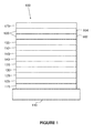
- FIG. 1 shows an organic light emitting device 100.
- Device 100 may include a substrate 110, an anode 115, a hole injection layer 120, a hole transport layer 125, an electron blocking layer 130, an emissive layer 135, a hole blocking layer 140, an electron transport layer 145, an electron injection layer 150, a protective layer 155, a cathode 160, and a barrier layer 170.
- Cathode 160 is a compound cathode having a first conductive layer 162 and a second conductive layer 164.
- Device 100 may be fabricated by depositing the layers described, in order. The properties and functions of these various layers, as well as example materials, are described in more detail in US 7,279,704 at cols. 6-10, which are incorporated by reference.
- each of these layers are available.
- a flexible and transparent substrate-anode combination is disclosed in U.S. Pat. No. 5,844,363 , which is incorporated by reference in its entirety.
- An example of a p-doped hole transport layer is m-MTDATA doped with F 4 -TCNQ at a molar ratio of 50:1, as disclosed in U.S. Patent Application Publication No. 2003/0230980 , which is incorporated by reference in its entirety.
- Examples of emissive and host materials are disclosed in U.S. Pat. No. 6,303,238 to Thompson et al. , which is incorporated by reference in its entirety.
- An example of an n-doped electron transport layer is BPhen doped with Li at a molar ratio of 1:1, as disclosed in U.S. Patent Application Publication No. 2003/0230980 , which is incorporated by reference in its entirety.
- U.S. Pat. Nos. 5,703,436 and 5,707,745 which are incorporated by reference in their entireties, disclose examples of cathodes including compound cathodes having a thin layer of metal such as Mg:Ag with an overlying transparent, electrically-conductive, sputter-deposited ITO layer.
- the theory and use of blocking layers is described in more detail in U.S. Pat. No. 6,097,147 and U.S. Patent Application Publication No.
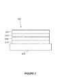
- FIG. 2 shows an inverted OLED 200.
- the device includes a substrate 210, a cathode 215, an emissive layer 220, a hole transport layer 225, and an anode 230.
- Device 200 may be fabricated by depositing the layers described, in order. Because the most common OLED configuration has a cathode disposed over the anode, and device 200 has cathode 215 disposed under anode 230, device 200 may be referred to as an "inverted" OLED. Materials similar to those described with respect to device 100 may be used in the corresponding layers of device 200.
- FIG. 2 provides one example of how some layers may be omitted from the structure of device 100.
- FIGS. 1 and 2 The simple layered structure illustrated in FIGS. 1 and 2 is provided by way of non-limiting example, and it is understood that embodiments of the invention may be used in connection with a wide variety of other structures.
- the specific materials and structures described are exemplary in nature, and other materials and structures may be used.
- Functional OLEDs may be achieved by combining the various layers described in different ways, or layers may be omitted entirely, based on design, performance, and cost factors. Other layers not specifically described may also be included. Materials other than those specifically described may be used. Although many of the examples provided herein describe various layers as comprising a single material, it is understood that combinations of materials, such as a mixture of host and dopant, or more generally a mixture, may be used. Also, the layers may have various sublayers.
- hole transport layer 225 transports holes and injects holes into emissive layer 220, and may be described as a hole transport layer or a hole injection layer.
- an OLED may be described as having an "organic layer" disposed between a cathode and an anode. This organic layer may comprise a single layer, or may further comprise multiple layers of different organic materials as described, for example, with respect to FIGS. 1 and 2 .
- OLEDs comprised of polymeric materials (PLEDs) such as disclosed in U.S. Pat. No. 5,247,190 to Friend et al. , which is incorporated by reference in its entirety.
- PLEDs polymeric materials
- OLEDs having a single organic layer may be used.
- OLEDs may be stacked, for example as described in U.S. Pat. No. 5,707,745 to Forrest et al , which is incorporated by reference in its entirety.
- the OLED structure may deviate from the simple layered structure illustrated in FIGS. 1 and 2 .
- the substrate may include an angled reflective surface to improve out-coupling, such as a mesa structure as described in U.S. Pat. No. 6,091,195 to Forrest et al. , and/or a pit structure as described in U.S. Pat. No. 5,834,893 to Bulovic et al. , which are incorporated by reference in their entireties.
- any of the layers of the various embodiments may be deposited by any suitable method.
- preferred methods include thermal evaporation, ink-jet, such as described in U.S. Pat. Nos. 6,013,982 and 6,087,196 , which are incorporated by reference in their entireties, organic vapor phase deposition (OVPD), such as described in U.S. Pat. No. 6,337,102 to Forrest et al. , which is incorporated by reference in its entirety, and deposition by organic vapor jet printing (OVJP), such as described in U.S. Pat. No. 7,431,968 , which is incorporated by reference in its entirety.
- OVPD organic vapor phase deposition
- OJP organic vapor jet printing
- Other suitable deposition methods include spin coating and other solution based processes.
- Solution based processes are preferably carried out in nitrogen or an inert atmosphere.
- preferred methods include thermal evaporation.
- Preferred patterning methods include deposition through a mask, cold welding such as described in U.S. Pat. Nos. 6,294,398 and 6,468,819 , which are incorporated by reference in their entireties, and patterning associated with some of the deposition methods such as ink-jet and OVJD. Other methods may also be used.
- the materials to be deposited may be modified to make them compatible with a particular deposition method. For example, substituents such as alkyl and aryl groups, branched or unbranched, and preferably containing at least 3 carbons, may be used in small molecules to enhance their ability to undergo solution processing.
- Substituents having 20 carbons or more may be used, and 3-20 carbons is a preferred range. Materials with asymmetric structures may have better solution processibility than those having symmetric structures, because asymmetric materials may have a lower tendency to recrystallize. Dendrimer substituents may be used to enhance the ability of small molecules to undergo solution processing.
- Devices fabricated in accordance with embodiments of the present invention may further optionally comprise a barrier layer.
- a barrier layer One purpose of the barrier layer is to protect the electrodes and organic layers from damaging exposure to harmful species in the environment including moisture, vapor and/or gases, etc.
- the barrier layer may be deposited over, under or next to a substrate, an electrode, or over any other parts of a device including an edge.
- the barrier layer may comprise a single layer, or multiple layers.
- the barrier layer may be formed by various known chemical vapor deposition techniques and may include compositions having a single phase as well as compositions having multiple phases. Any suitable material or combination of materials may be used for the barrier layer.
- the barrier layer may incorporate an inorganic or an organic compound or both.
- the preferred barrier layer comprises a mixture of a polymeric material and a non-polymeric material as described in U.S. Pat. No. 7,968,146 , PCT Pat. Application Nos. PCT/US2007/023098 and PCT/US2009/042829 , which are herein incorporated by reference in their entireties.
- the aforesaid polymeric and non-polymeric materials comprising the barrier layer should be deposited under the same reaction conditions and/or at the same time.
- the weight ratio of polymeric to non-polymeric material may be in the range of 95:5 to 5:95.
- the polymeric material and the non-polymeric material may be created from the same precursor material.
- the mixture of a polymeric material and a non-polymeric material consists essentially of polymeric silicon and inorganic silicon.
- Devices fabricated in accordance with embodiments of the invention can be incorporated into a wide variety of electronic component modules (or units) that can be incorporated into a variety of electronic products or intermediate components. Examples of such electronic products or intermediate components include display screens, lighting devices such as discrete light source devices or lighting panels, etc. that can be utilized by the end-user product manufacturers. Such electronic component modules can optionally include the driving electronics and/or power source(s). Devices fabricated in accordance with embodiments of the invention can be incorporated into a wide variety of consumer products that have one or more of the electronic component modules (or units) incorporated therein. Such consumer products would include any kind of products that include one or more light source(s) and/or one or more of some type of visual displays.
- Some examples of such consumer products include flat panel displays, computer monitors, medical monitors, televisions, billboards, lights for interior or exterior illumination and/or signaling, heads-up displays, fully or partially transparent displays, flexible displays, laser printers, telephones, cell phones, tablets, phablets, personal digital assistants (PDAs), laptop computers, digital cameras, camcorders, viewfinders, micro-displays, 3-D displays, vehicles, a large area wall, theater or stadium screen, or a sign.
- PDAs personal digital assistants
- Various control mechanisms may be used to control devices fabricated in accordance with the present invention, including passive matrix and active matrix. Many of the devices are intended for use in a temperature range comfortable to humans, such as 18 degrees C. to 30 degrees C., and more preferably at room temperature (20-25 degrees C), but could be used outside this temperature range, for example, from -40 degree C to + 80 degree C.
- the materials and structures described herein may have applications in devices other than OLEDs.
- other optoelectronic devices such as organic solar cells and organic photodetectors may employ the materials and structures.
- organic devices such as organic transistors, may employ the materials and structures.
- halo includes fluorine, chlorine, bromine, and iodine.
- alkyl as used herein contemplates both straight and branched chain alkyl radicals.
- Preferred alkyl groups are those containing from one to fifteen carbon atoms and includes methyl, ethyl, propyl, isopropyl, butyl, isobutyl, tert-butyl, and the like. Additionally, the alkyl group may be optionally substituted.
- cycloalkyl as used herein contemplates cyclic alkyl radicals.
- Preferred cycloalkyl groups are those containing 3 to 7 carbon atoms and includes cyclopropyl, cyclopentyl, cyclohexyl, and the like. Additionally, the cycloalkyl group may be optionally substituted.
- alkenyl as used herein contemplates both straight and branched chain alkene radicals.
- Preferred alkenyl groups are those containing two to fifteen carbon atoms. Additionally, the alkenyl group may be optionally substituted.
- alkynyl as used herein contemplates both straight and branched chain alkyne radicals. Preferred alkynyl groups are those containing two to fifteen carbon atoms. Additionally, the alkynyl group may be optionally substituted.
- aralkyl or "arylalkyl” as used herein are used interchangeably and contemplate an alkyl group that has as a substituent an aromatic group. Additionally, the aralkyl group may be optionally substituted.
- heterocyclic group contemplates aromatic and non-aromatic cyclic radicals.
- Hetero-aromatic cyclic radicals also means heteroaryl.
- Preferred hetero-non-aromatic cyclic groups are those containing 3 or 7 ring atoms which includes at least one hetero atom, and includes cyclic amines such as morpholino, piperdino, pyrrolidino, and the like, and cyclic ethers, such as tetrahydrofuran, tetrahydropyran, and the like. Additionally, the heterocyclic group may be optionally substituted.
- aryl or "aromatic group” as used herein contemplates single-ring groups and polycyclic ring systems.
- the polycyclic rings may have two or more rings in which two carbons are common to two adjoining rings (the rings are "fused") wherein at least one of the rings is aromatic, e.g., the other rings can be cycloalkyls, cycloalkenyls, aryl, heterocycles, and/or heteroaryls. Additionally, the aryl group may be optionally substituted.
- heteroaryl as used herein contemplates single-ring hetero-aromatic groups that may include from one to three heteroatoms, for example, pyrrole, furan, thiophene, imidazole, oxazole, thiazole, triazole, pyrazole, pyridine, pyrazine and pyrimidine, and the like.
- heteroaryl also includes polycyclic hetero-aromatic systems having two or more rings in which two atoms are common to two adjoining rings (the rings are "fused") wherein at least one of the rings is a heteroaryl, e.g., the other rings can be cycloalkyls, cycloalkenyls, aryl, heterocycles, and/or heteroaryls. Additionally, the heteroaryl group may be optionally substituted.
- alkyl, cycloalkyl, alkenyl, alkynyl, aralkyl, heterocyclic group, aryl, and heteroaryl may be optionally substituted with one or more substituents selected from the group consisting of hydrogen, deuterium, halogen, alkyl, cycloalkyl, heteroalkyl, arylalkyl, alkoxy, aryloxy, amino, cyclic amino, silyl, alkenyl, cycloalkenyl, heteroalkenyl, alkynyl, aryl, heteroaryl, acyl, carbonyl, carboxylic acid, ether, ester, nitrile, isonitrile, sulfanyl, sulfinyl, sulfonyl, phosphino, and combinations thereof.
- substituted indicates that a substituent other than H is bonded to the relevant position, such as carbon.
- substituent other than H such as carbon.
- R 1 is mono-substituted
- one R 1 must be other than H.
- R 1 is di-substituted
- two of R 1 must be other than H.
- R 1 is hydrogen for all available positions.
- aza-dibenzofuran i.e. aza-dibenzofuran, aza-dibenzothiophene, etc.
- azatriphenylene encompasses both dibenzo[ f,h ]quinoxaline and dibenzo[ f,h ]quinoline.
- the emissive layer (EML) of OLED devices exhibiting good lifetime and efficiency requires more than two components (e.g. 3 or 4 components). Fabricating such EMLs using vacuum thermal evaporation (VTE) process then requires evaporating 3 or 4 evaporation source materials in separate VTE sublimation crucibles, which is very complicated and costly compared to a standard two-component EML with a single host and an emitter, which requires only two evaporation sources.
- VTE vacuum thermal evaporation
- Premixing two or more materials and evaporating them from one VTE sublimation crucible can reduce the complexity of the fabrication process.
- the co-evaporation must be stable and produce an evaporated film having a composition that remains constant through the evaporation process. Variations in the film's composition may adversely affect the device performance.
- the materials In order to obtain a stable co-evaporation from a mixture of compounds under vacuum, one would assume that the materials must have the same evaporation temperature under the same condition. However, this may not be the only parameter one has to consider.
- two compounds When two compounds are mixed together, they may interact with each other and the evaporation property of the mixture may differ from their individual properties.
- materials with slightly different evaporation temperatures may form a stable co-evaporation mixture.
- Evaporation temperature of a material is measured in a vacuum deposition tool at a constant pressure, normally between 1x10 -7 Torr to 1x10 -8 Torr, at a 2 ⁇ /sec deposition rate on a surface positioned at a set distance away from the evaporation source of the material being evaporated, e.g. sublimation crucible in a VTE tool.
- the various measured values such as temperature, pressure, deposition rate, etc. disclosed herein are expected to have nominal variations because of the expected tolerances in the measurements that produced these quantitative values as understood by one of ordinary skill in the art.
- Mass loss rate of a material is defined as the percentage of mass lost over time (“percentage/minute” or "%/min”) and is determined by measuring the time it takes to lose the first 10% of the mass of a sample of the material as measured by thermal gravity analysis (TGA) under a given experimental condition at a given constant temperature for a given material after the a steady evaporation state is reached.
- the given constant temperature is one temperature point that is chosen so that the value of mass loss rate is between about 0.05 to 0.50 %/min.
- a skilled person in this field should appreciate that in order to compare two parameters, the experimental condition should be consistent.
- the method of measuring mass loss rate and vapor pressure is well known in the art and can be found, for example, in Bull. et al. Mater. Sci. 2011, 34, 7 .
- the EML may consist of three or more components.
- the EML can consist of two host-type compounds and an emitter combination (e.g. a hole transporting cohost (h-host), an electron transporting cohost (e-host), and a compound capable of functioning as an emitter in an OLED at room temperature).
- the EML can consist of one host-type compound and two emitter-type compounds (e.g., a host compound and two compounds each capable of functioning as an emitter in an OLED at room temperature).
- h-host hole transporting cohost
- e-host electron transporting cohost
- the EML can consist of one host-type compound and two emitter-type compounds (e.g., a host compound and two compounds each capable of functioning as an emitter in an OLED at room temperature).
- three or more evaporation sources are required, one for each of the components.
- the concentration of the components are important for the device performance, typically, the rate of deposition of each component is measured individually during the deposition process. This makes the VTE process complicated and costly. Thus, it is desired to premix at least two of the components of such EMLs to reduce the number of VTE evaporation sources.
- any two of the three or more components of the EMLs can be premixed and form a stable mixture of co-evaporation source, then the number of evaporation sources required for EML layer fabrication would be reduced.
- materials to be premixable into an evaporation source they should co-evaporate and deposit uniformly without changing the ratio.
- the ratio of the components in the mixture should be the same as the ratio of the components in the evaporation deposited films from these premixed materials. Therefore, the concentration of the two components in the deposited film is controlled by their concentration in the premixed evaporation source.
- This disclosure describes a new class of h- and e-hosts that can be premixed and stably co-evaporated from a single source.
- a composition of materials comprising a first compound.
- the first compound has a structure of formula: In Formula I:
- one or more of L 1 , L 2 and L 3 can be a direct bond, and the direct bond can be a single bond or a double bond.
- L 1 is a direct bond
- n 0.
- n is 0, while n is equal to or greater than 1 in other embodiments.
- m and n are both 0.
- m is equal to or greater than 1.
- G 4 has the structure selected from the group consisting of:
- G 1 has the structure selected from the group consisting of: wherein:
- L 1 is selected from the group consisting of:
- G 2 , G 3 and G 5 are independently selected from the group consisting of: and wherein
- At least one of G 2 , G 3 , G 4 and G 5 is substituted with at least one fluorine atom.
- the first compound has the formula: where X is selected from a group consisting of O, S and Se.
- the first compound is selected from the group consisting of:
- n is 0, m is 1, and G 4 -G 1 has a structure selected from the group consisting of: and
- the first compound is selected from the group consisting of: and
- the first compound has a formula: where L 1 is biphenyl.
- the first compound is selected from the group consisting of: and
- the composition comprises a second compound having a structure of formula II: Formula II.
- Formula II In the structure of Formula II:
- the second compound is selected from the group consisting of where:
- the second compound is selected from the group consisting of
- the mixture of the first compound and the second compound is selected from the group consisting of: and
- the mixture of the first compound and the second compound is selected from the group consisting of:
- the composition comprises a second compound, where the second compound is a phosphorescent emissive Ir complex having at least one substituent selected from the group consisting of alkyl, cycloalkyl, partially or fully deuterated variants thereof, partially or fully fluorinated variants thereof, and combinations thereof.
- the second compound is a phosphorescent emissive Ir complex having at least one substituent selected from the group consisting of alkyl, cycloalkyl, partially or fully deuterated variants thereof, partially or fully fluorinated variants thereof, and combinations thereof.
- composition of materials comprising a first compound having a structure of: Formula III, is disclosed.
- a first compound having a structure of: Formula III is disclosed.
- one or more of L A and L B can be a direct bond, and the direct bond can be a single bond or a double bond.
- the first compound is selected from the group consisting of:
- the first compound has an evaporation temperature T1 of 150 to 350 °C; the second compound has an evaporation temperature T2 of 150 to 350 °C; an absolute value of T1-T2 is less than 20 °C; the first compound has a concentration C1 in said mixture and a concentration C2 in a film formed by evaporating the mixture in a vacuum deposition tool at a constant pressure between 1x10 -6 Torr to 1x10 -9 Torr, at a 2 ⁇ /sec deposition rate on a surface positione at a predefined distance away from the mixture being evaporated; and the absolute value of (C1-C2)/C1 is less than 5%.
- the first compound has a vapor pressure of P1 at T1 at 1 atm
- the second compound has a vapor pressure of P2 at T2 at 1 atm
- the ratio of P1/P2 is within the range of 0.90 to 1.10.
- the first compound has a first mass loss rate and the second compound has a second mass loss rate, wherein the ratio between the first mass loss rate and the second mass loss rate is within the range of 0.90 to 1.10.
- the first compound and the second compound each has a purity in excess of 99 % as determined by high pressure liquid chromatography.
- the composition also comprises a third compound.
- the third compound has a different chemical structure than the first and second compounds.
- the third compound has a third mass loss rate and the ratio between the first mass loss rate and third mass loss rate is within the range of 0.90 to 1.10.
- the third compound has an evaporation temperature T3 of 150 to 350 °C, and the absolute value of T1-T3 is less than 20 °C.
- the composition is in liquid form at a temperature less than T1 and T2.
- the composition comprises a second compound, where the second compound has the formula IV of having the structure:
- Ar 4 is selected from the group consisting of aryl, heteroaryl, alkyl, cycloalkyl and combinations thereof;
- L 11 and L 12 are each independently selected from the group consisting of a direct bond, aryl, heteroaryl, alkyl, alkoxyl, and combinations thereof;
- p is an integer from 0 to 20; when p is greater than 1, each G 7 can be same or different;
- R 11 , R 13 , R 15 , and R 16 each independently represents mono, di, tri, or tetra substitution, or no substitution;
- R 12 and R 14 each independently represent mono, di, or tri substitution, or no substitution;
- R 11 , R 12 , R 13 , R 14 , R 15 , and R 16 are each independently selected from the group consisting of hydrogen, deuterium, halogen, alkyl, cycloalkyl, silyl, carbonyl, alkyloxy
- the second compound is selected from the group consisting of:
- the second compound is selected from the group consisting of:
- the mixture of the first compound and the second compound is selected from the group consisting of: and
- the mixture of the first compound and the second compound is
- the first compound has an evaporation temperature T1 of 150 to 350 °C
- the second compound has an evaporation temperature T2 of 150 to 350 °C, or both.
- the absolute value of T1-T2 is less than 20 °C.
- the first compound has a concentration C1 in said mixture and a concentration C2 in a film formed by evaporating the mixture in a vacuum deposition tool at a constant pressure between 1x10 -6 Torr to 1x10 -9 Torr, at a 2 ⁇ /sec deposition rate on a surface positione at a predefined distance away from the mixture being evaporated.
- the absolute value of (C1-C2)/C1 is less than 5%.
- the first compound has a vapor pressure of P1 at T1 at 1 atm
- the second compound has a vapor pressure of P2 at T2 at 1 atm
- the ratio of P1/P2 is within the range of 0.90 to 1.10.
- the first compound has a first mass loss rate and the second compound has a second mass loss rate, where the ratio between the first mass loss rate and the second mass loss rate is within the range of 0.90 to 1.10.
- the first compound and the second compound each has a purity in excess of 99 % as determined by high pressure liquid chromatography.
- the composition further comprises a third compound, where the third compound has a different chemical structure than the first and second compounds.
- the third compound has an evaporation temperature T3 of 150 to 350 °C, and wherein absolute value of T1-T3 is less than 20 °C.
- the third compound has a third mass loss rate and the ratio between the first mass loss rate and third mass loss rate is within the range of 0.90 to 1.10.
- the composition is in liquid form at a temperature less than T1 and T2.
- a device that includes one or more organic light emitting devices. At least one of the one or more organic light emitting devices can include an anode, a cathode, and an organic layer, disposed between the anode and the cathode.
- the organic layer can include a composition comprising a compound according to a structure of Formula I or Formula III, or any of the variations thereof described herein.
- the organic layer is an emissive layer and the composition comprises a host.
- the organic layer also includes a phosphorescent emissive dopant.
- the phosphorescent emissive dopant is a transition metal complex having at least one ligand or part of the ligand if the ligand is more than bidentate selected from the group consisting of: and where:
- the organic layer is a blocking layer and the composition is a blocking material in the organic layer.
- the organic layer is an electron transporting layer and the composition is an electron transporting material in the organic layer.
- the first device is selected from the group consisting of a consumer product, an electronic component module, an organic light-emitting device, and a lighting panel.
- At least one of R a , R b , R c , and R d is selected from the group consisting of alkyl, cycloalkyl, partially or fully deuterated variants thereof, partially or fully fluorinated variants thereof, and combinations thereof.
- the organic light emitting device can include a first electrode, a second electrode, and a first organic layer disposed between the first electrode and the second electrode, where the first organic layer comprises a first composition comprising a mixture of a first compound and a second compound.
- the method includes providing a substrate having the first electrode disposed thereon; depositing the first composition over the first electrode; and depositing the second electrode over the first organic layer.
- the first composition is selected from the group consisting of Formulation I and Fomulation II, where Formulation I comprises a first compound of Formula I and a second compound of Formula II, and where Formulation II comprises a first compound of Formula III and a second compound of Formula IV.
- the materials described herein as useful for a particular layer in an organic light emitting device may be used in combination with a wide variety of other materials present in the device.
- emissive dopants disclosed herein may be used in conjunction with a wide variety of hosts, transport layers, blocking layers, injection layers, electrodes and other layers that may be present.
- the materials described or referred to below are non-limiting examples of materials that may be useful in combination with the compounds disclosed herein, and one of skill in the art can readily consult the literature to identify other materials that may be useful in combination.
- a hole injecting/transporting material to be used in the present invention is not particularly limited, and any compound may be used as long as the compound is typically used as a hole injecting/transporting material.
- the material include, but are not limited to: a phthalocyanine or porphyrin derivative; an aromatic amine derivative; an indolocarbazole derivative; a polymer containing fluorohydrocarbon; a polymer with conductivity dopants; a conducting polymer, such as PEDOT/PSS; a self-assembly monomer derived from compounds such as phosphonic acid and silane derivatives; a metal oxide derivative, such as MoO x ; a p-type semiconducting organic compound, such as 1,4,5,8,9,12-Hexaazatriphenylenehexacarbonitrile; a metal complex, and a cross-linkable compound.
- aromatic amine derivatives used in HIL or HTL include, but are not limited to the following general structures:
- Each of Ar 1 to Ar 9 is selected from the group consisting aromatic hydrocarbon cyclic compounds such as benzene, biphenyl, triphenyl, triphenylene, naphthalene, anthracene, phenalene, phenanthrene, fluorene, pyrene, chrysene, perylene, azulene; group consisting aromatic heterocyclic compounds such as dibenzothiophene, dibenzofuran, dibenzoselenophene, furan, thiophene, benzofuran, benzothiophene, benzoselenophene, carbazole, indolocarbazole, pyridylindole, pyrrolodipyridine, pyrazole, imidazole, triazole, oxazole, thiazole, oxadiazole, oxatriazole, dioxazole, thiadiazole, pyridine, pyridazine, pyrim
- each Ar is further substituted by a substituent selected from the group consisting of hydrogen, deuterium, halide, alkyl, cycloalkyl, heteroalkyl, arylalkyl, alkoxy, aryloxy, amino, silyl, alkenyl, cycloalkenyl, heteroalkenyl, alkynyl, aryl, heteroaryl, acyl, carbonyl, carboxylic acids, ester, nitrile, isonitrile, sulfanyl, sulfinyl, sulfonyl, phosphino, and combinations thereof.
- a substituent selected from the group consisting of hydrogen, deuterium, halide, alkyl, cycloalkyl, heteroalkyl, arylalkyl, alkoxy, aryloxy, amino, silyl, alkenyl, cycloalkenyl, heteroalkenyl, alkynyl, aryl, heteroaryl, acy
- Ar 1 to Ar 9 is independently selected from the group consisting of: wherein k is an integer from 1 to 20; X 101 to X 108 is C (including CH) or N; Z 101 is NAr 1 , O, or S; Ar 1 has the same group defined above.
- metal complexes used in HIL or HTL include, but are not limited to the following general formula: wherein Met is a metal, which can have an atomic weight greater than 40; (Y 101 -Y 102 ) is a bidentate ligand, Y 101 and Y 102 are independently selected from C, N, O, P, and S; L 101 is an ancillary ligand; k' is an integer value from 1 to the maximum number of ligands that may be attached to the metal; and k'+k" is the maximum number of ligands that may be attached to the metal.
- (Y 101 -Y 102 ) is a 2-phenylpyridine derivative. In another aspect, (Y 101 -Y 102 ) is a carbene ligand. In another aspect, Met is selected from Ir, Pt, Os, and Zn. In a further aspect, the metal complex has a smallest oxidation potential in solution vs. Fc + /Fc couple less than about 0.6 V.
- the light emitting layer of the organic EL device of the present invention preferably contains at least a metal complex as light emitting material, and may contain a host material using the metal complex as a dopant material.
- the host material are not particularly limited, and any metal complexes or organic compounds may be used as long as the triplet energy of the host is larger than that of the dopant. While the Table below categorizes host materials as preferred for devices that emit various colors, any host material may be used with any dopant so long as the triplet criteria is satisfied.
- Examples of metal complexes used as host are preferred to have the following general formula: wherein Met is a metal; (Y 103 -Y 104 ) is a bidentate ligand, Y 103 and Y 104 are independently selected from C, N, O, P, and S; L 101 is an another ligand; k' is an integer value from 1 to the maximum number of ligands that may be attached to the metal; and k'+k" is the maximum number of ligands that may be attached to the metal.
- the metal complexes are: wherein (O-N) is a bidentate ligand, having metal coordinated to atoms O and N.
- Met is selected from Ir and Pt.
- (Y 103 -Y 104 ) is a carbene ligand.
- organic compounds used as host are selected from the group consisting aromatic hydrocarbon cyclic compounds such as benzene, biphenyl, triphenyl, triphenylene, naphthalene, anthracene, phenalene, phenanthrene, fluorene, pyrene, chrysene, perylene, azulene; group consisting aromatic heterocyclic compounds such as dibenzothiophene, dibenzofuran, dibenzoselenophene, furan, thiophene, benzofuran, benzothiophene, benzoselenophene, carbazole, indolocarbazole, pyridylindole, pyrrolodipyridine, pyrazole, imidazole, triazole, oxazole, thiazole, oxadiazole, oxatriazole, dioxazole, thiadiazole, pyridine, pyridazine, pyrimidine
- each group is further substituted by a substituent selected from the group consisting of hydrogen, deuterium, halide, alkyl, cycloalkyl, heteroalkyl, arylalkyl, alkoxy, aryloxy, amino, silyl, alkenyl, cycloalkenyl, heteroalkenyl, alkynyl, aryl, heteroaryl, acyl, carbonyl, carboxylic acids, ester, nitrile, isonitrile, sulfanyl, sulfinyl, sulfonyl, phosphino, and combinations thereof.
- a substituent selected from the group consisting of hydrogen, deuterium, halide, alkyl, cycloalkyl, heteroalkyl, arylalkyl, alkoxy, aryloxy, amino, silyl, alkenyl, cycloalkenyl, heteroalkenyl, alkynyl, aryl, heteroaryl, acy
- host compound contains at least one of the following groups in the molecule: wherein R 101 to R 107 is independently selected from the group consisting of hydrogen, deuterium, halide, alkyl, cycloalkyl, heteroalkyl, arylalkyl, alkoxy, aryloxy, amino, silyl, alkenyl, cycloalkenyl, heteroalkenyl, alkynyl, aryl, heteroaryl, acyl, carbonyl, carboxylic acids, ester, nitrile, isonitrile, sulfanyl, sulfinyl, sulfonyl, phosphino, and combinations thereof, when it is aryl or heteroaryl, it has the similar definition as Ar's mentioned above.
- k is an integer from 0 to 20 or 1 to 20; k"' is an integer from 0 to 20.
- X 101 to X 108 is selected from C (including CH) or N.
- Z 101 and Z 102 is selected from NR 101 , O, or S.
- a hole blocking layer may be used to reduce the number of holes and/or excitons that leave the emissive layer.
- the presence of such a blocking layer in a device may result in substantially higher efficiencies as compared to a similar device lacking a blocking layer.
- a blocking layer may be used to confine emission to a desired region of an OLED.
- compound used in HBL contains the same molecule or the same functional groups used as host described above.
- compound used in HBL contains at least one of the following groups in the molecule: wherein k is an integer from 1 to 20; L 101 is an another ligand, k' is an integer from 1 to 3.
- Electron transport layer may include a material capable of transporting electrons. Electron transport layer may be intrinsic (undoped), or doped. Doping may be used to enhance conductivity. Examples of the ETL material are not particularly limited, and any metal complexes or organic compounds may be used as long as they are typically used to transport electrons.
- compound used in ETL contains at least one of the following groups in the molecule: wherein R 101 is selected from the group consisting of hydrogen, deuterium, halide, alkyl, cycloalkyl, heteroalkyl, arylalkyl, alkoxy, aryloxy, amino, silyl, alkenyl, cycloalkenyl, heteroalkenyl, alkynyl, aryl, heteroaryl, acyl, carbonyl, carboxylic acids, ester, nitrile, isonitrile, sulfanyl, sulfinyl, sulfonyl, phosphino, and combinations thereof, when it is aryl or heteroaryl, it has the similar definition as Ar's mentioned above.
- Ar 1 to Ar 3 has the similar definition as Ar's mentioned above.
- k is an integer from 1 to 20.
- X 101 to X 108 is selected from C (including CH) or N.
- the metal complexes used in ETL include, but are not limited to the following general formula: wherein (O-N) or (N-N) is a bidentate ligand, having metal coordinated to atoms O, N or N, N; L 101 is another ligand; k' is an integer value from 1 to the maximum number of ligands that may be attached to the metal.
- the hydrogen atoms can be partially or fully deuterated.
- any specifically listed substituent such as, without limitation, methyl, phenyl, pyridyl, etc. encompasses undeuterated, partially deuterated, and fully deuterated versions thereof.
- classes of substituents such as, without limitation, alkyl, aryl, cycloalkyl, heteroaryl, etc. also encompass undeuterated, partially deuterated, and fully deuterated versions thereof.
- hole injection materials In addition to and / or in combination with the materials disclosed herein, many hole injection materials, hole transporting materials, host materials, dopant materials, exciton/hole blocking layer materials, electron transporting and electron injecting materials may be used in an OLED.
- Non-limiting examples of the materials that may be used in an OLED in combination with materials disclosed herein are listed in Table A below. Table A lists non-limiting classes of materials, non-limiting examples of compounds for each class, and references that disclose the materials. TABLE A MATERIAL EXAMPLES OF MATERIAL PUBLICATIONS Hole injection materials Phthalocyanine and porphyrin compounds Appl. Phys. Lett. 69, 2160 (1996 ) Starburst triarylamines J. Lumin.
- Dibenzo[ b,d ]thiophen-4-ylboronic acid (3.0 g, 13.15 mmol) and 1,3-dibromo-5-chlorobenzene (10.67 g, 39.5 mmol) were dissolved in toluene (150 ml) under a nitrogen atmosphere in a nitrogen-flushed 250 mL two-necked round-bottomed flask to give a colorless solution.
- K 2 CO 3 (7.27 g, 52.6 mmol) in water (50 ml) was added to the reaction mixture, followed by Pd(PPh 3 ) 4 (0.304 g, 0.263 mmol). The reaction mixture was then heated to reflux under nitrogen overnight ( ⁇ 12 hours).
- the reaction mixture was gradually warmed to room tempeature ( ⁇ 22°C) and stirred for 16 h before quenching with a 10% NH 4 Cl aqeous solution.
- the resulting mixture was extracted with ethyl acetate. After evaporating the solvent, the residue was purified by column chromatography on silica gel with heptane/DCM (1/1, v/v) as the eluent and then recrystallized from heptane to yield 2-(2,8-diphenyldibenzo[ b,d ]thiophen-4-yl)-4,4,5,5-tetramethyl-1,3,2-dioxaborolane (5.5 g, 53.7%) as white crystals.
- the reaction mixture was gradually warmed to room tempeature ( ⁇ 22°C) and stirred for 16 h before being quenched with a 10% NH 4 Cl aqeous solution.
- the resulting mixture was extracted with ethyl acetate. After evaporating the solvent, the residue was purified by column chromatography on silica gel with heptane/DCM (4/1 to 0/1, v/v) as the eluent, then recrystallized from heptane to yield 2-(6,8-diphenyldibenzo[ b,d ]thiophen-4-yl)-4,4,5,5-tetramethyl-1,3,2-dioxaborolane (9.5 g, 69%) as white crystals.
- OLED organic light-emitting diode
- the anode electrode was 80 nm of indium tin oxide (ITO).
- the cathode electrode consisted of 1 nm of LiF followed by 100 nm of Al. All devices were encapsulated with a glass lid sealed with an epoxy resin in a nitrogen glove box ( ⁇ 1 ppm of H 2 O and O 2 ) immediately after fabrication, and a moisture getter was incorporated inside the package.
- a first set of device examples have organic stacks consisting of, sequentially, from the ITO surface, 10 nm of LG101 (from LG Chem) as the hole injection layer (HIL), 45 nm of 4,4'-bis[N-(1-naphthyl)-N-phenylaminolbiphenyl (NPD) as the hole-transport layer (HTL), and 30 nm of Compound E8 with 20 wt% of inventive compound (Compound C65) or comparative compound (CC-1) and 10 wt% of emitter GD as the emissive layer (EML).
- LG101 from LG Chem
- NPD 4,4'-bis[N-(1-naphthyl)-N-phenylaminolbiphenyl
- HTL hole-transport layer
- Compound E8 with 20 wt% of inventive compound (Compound C65) or comparative compound (CC-1) and 10 wt% of emitter GD as the emissive layer (EM
- HBL hole blocking layer
- ETL electron-transport layer
- Table D1 is a summary of the device data, voltage (V), external efficiency (EQE) and power efficiency (PE), recorded at 9000 nits for the Device Example 1.
- Table D1 shows that Device 1 using inventive compound Compound C65 as the co-host and HBL achieves higher efficiency at a lower driving voltage than Device C-1 using comparative compound CC-1 as the co-host and HBL.
- Device Examples - Set 2 A second set of device examples have the same structure as that in Device Example 1 except that an inventive Compound C101 or a comparative compound CC-2 doped with 15% of GD is used as a two-component EML.
- inventive Compound C101 or a comparative compound CC-2 doped with 15% of GD is used as a two-component EML.
- the chemical structures of the inventive and comparative compounds used are presented below.
- Table D2 is a summary of the relative device data recorded at 9000 nits for the Device Example 2.
- Device lifetime LT97 is defined as the time it takes for devices to decay to 97% of their original luminance under a constant current density with an initial luminance of 9000 nits, and the values are normalized to that of Device C-2.
- Table D2 Device EML HBL Color V (V) EQE (%) PE (lm/W) LT97
- Table D2 shows that Device 2 using inventive compound Compound C101 as the host and HBL achieves higher efficiency and longer lifetime than Device C-2 using comparative compound CC-2 as the host and HBL.
- Device Examples - Set 3 A third set of device examples have the same structure as that in Device Example 1.
- the chemical structures of the inventive and comparative compounds used are presented below.
- Table D3 is a summary of the relative device data recorded at 1000 nits for the Device Examples 3.
- Device lifetime LT95 defined as the time it takes for devices to decay to 95% of their original luminance under a constant current density with an initial luminance of 1000 nits, was calculated, with an acceleration factor of 1.8, from the values measured at a current density of 50 mA/cm 2 , and normalized to that of Device C-3.
- Device Examples - Set 4 A fourth set of devices have the same structure as that in Device Example 2.
- the chemical structures of the inventive and comparative compounds used are presented below. and
- Table D4 is a summary of the relative device data recorded at 1000 nits for the Device Example 4.
- Device lifetime LT95 was normalized to that of Device C-4.
- Device Examples - Set 5 A fifth set of devices have the same structure as that in Device Example 1.
- the chemical structures of the inventive and comparative compounds used are presented below.
- Table D5 is a summary of the relative device data recorded at 9000 nits for the Device Example 5.
- Device lifetime LT97 is defined as the time it takes for devices to decay to 97% of their original luminance under a constant current density with an initial luminance of 9000 nits, and the values are normalized to that of Device C-11.
- Table D5 Device EML HBL Color V (V) EQE (%) PE (lm/W) LT97
- Table D5 shows that Device 31 using inventive compound Compound D2 as the host and HBL achieves higher efficiency and longer lifetime than Device C-11 using comparative compound CC-11 as the host and HBL.
- Table PM1 Potential premixtures comprising selected h- and e-hosts Premixtures h-hosts e-hosts PM-A1 Compound E1 Compound C 1 PM-A2 Compound E2 Compound C2 PM-A3 Compound E5 Compound C65 PM-A4 Compound E8 Compound C74 PM-A5 Compound E11 Compound C74 PM-A6 Compound E17 Compound C74 PM-A7 Compound E8 CC-1 PM-A8 Compound E8 Compound A5 PM-A9 Compound E8 Compound C17 PM-A10 Compound E17 Compound A5 PM-A11 Compound E25 CC-1 PM-A12 Compound E26 Compound C74 PM-A13 Compound E26 Compound C248 PM-A14 Compound E28 Compound C74 PM-A15 Compound E29 Compound C74 PM-A16 Compound E30 Compound C74
- Premixture Example - Set 1 For premixture PM-A4, Compound E8 and Compound C74 were provided at a weight ratio of 7:3, then they were physically mixed, grinded and loaded into an evaporation source. The premixed compositions were thermally co-evaporated at a rate of 2 ⁇ /s in a vacuum chamber under a pressure less than 10 -7 Torr, and deposited onto glass substrates. The substrates were replaced continuously after deposition of 500 ⁇ of film without stopping the deposition and cooling the source. The compositions of films were analyzed by high-performance liquid chromatography (HPLC) and the results are shown in Table 2.
- HPLC high-performance liquid chromatography
- Table PM2 HPLC composition (%) of sequentially deposited films from premixture (PM-A4) comprising Compound E8 and Compound C74 with weight ratio 7:3.
- HPLC Conditions C18, 100 45 min, Detected wavelength 254 nm (Due to different absorption coefficients, the HPLC composition may or may not agree with the weight ratio.)
- Premixture Example - Set 2 For premixture PM-A12, Compound E26 and Compound C74 were provided at a weight ratio of 3:2, then they were physically mixed, grinded, and loaded into an evaporation source.
- the premixed compositions were thermally co-evaporated at a rate of 2 ⁇ /s in a vacuum chamber under a pressure less than 10 -7 Torr, and deposited onto glass substrates. The substrates were replaced continuously after deposition of 500 ⁇ of film without stopping the deposition and cooling the source.
- the compositions of films were analyzed by high-performance liquid chromatography (HPLC) and the results are shown in Table PM3.
- Table PM3 HPLC composition (%) of sequentially deposited films from premixture (PM-A12) comprising Compound E26 and Compound C74 with weight ratio 3:2.
- HPLC Conditions C18, 100 45 min, Detected wavelength 254 nm (Due to different absorption coefficients, the HPLC composition may or may not agree with the weight ratio.)
- Premixture Example - Set 3 For premixture PM-A16, Compound E30 and Compound C74 were provided at a weight ratio of 1:1, then they were physically mixed, grinded and loaded into an evaporation source. The premixed compositions were thermally co-evaporated at a rate of 2 ⁇ /s in a vacuum chamber under a pressure less than 10 -7 Torr, and deposited onto glass substrates. The substrates were replaced continuously after deposition of 500 ⁇ of film without stopping the deposition and cooling the source. The compositions of films were analyzed by high-performance liquid chromatography (HPLC) and the results are shown in Table PM4.
- HPLC high-performance liquid chromatography
- Table PM4 HPLC composition (%) of sequentially deposited films from premixture (PM-A16) comprising Compound E30 and Compound C74 with weight ratio 1:1. (HPLC Conditions C18, 100 45 min, Detected wavelength 254 nm) (Due to different absorption coefficients, the HPLC composition may or may not agree with the weight ratio.) Films Compound E30 Compound C74 Plate1 52.3 47.7 Plate2 51.6 48.4 Plate3 52.1 47.9 Plate4 52.9 47.1 Plate5 53.9 46.1 Plate6 54.6 45.4 Plate7 51.8 48.2
- Table PM5 A second set of potential premixtures of selected h- and e-hosts are presented in Table PM5.
- Table PM5 Potential premixtures comprising selected h- and e-hosts Premixtures h-hosts e-hosts PM-B1 Compound G1 Compound F9 PM-B2 Compound G2 Compound F10 PM-B3 Compound G8 Compound F13 PM-B4 Compound G9 Compound F13 PM-B5 Compound G26 Compound F5
- Example 1 For premixture PM-B3, Compound G8 and Compound F13 were provided at a weight ratio of 9:1, then they were physically mixed, grinded and loaded into an evaporation source.
- the premixed compositions were thermally co-evaporated at a rate of 2 ⁇ /s in a vacuum chamber under a pressure less than 10 -7 Torr, and deposited onto glass substrates.
- the substrates were replaced continuously after deposition of 500 ⁇ of film without stopping the deposition or cooling the source. The deposition was stopped upon material depletion.
- the compositions of films were analyzed by high-performance liquid chromatography (HPLC) and the results are shown in Table PM6.
- Table PM6 HPLC composition (%) of sequentially deposited films from premixture (PM-B3) comprising Compound G8 and Compound F13 with weight ratio 9:1. (HPLC Conditions C18, 100 45 min, Detection wavelength 254 nm) (Due to different absorption coefficients, the HPLC composition may or may not agree with the weight ratio.) Table PM6 Films Compound G8 Compound F13 Plate1 95.9 4.1 Plate2 96.0 4.0 Plate3 96.5 3.5 Plate4 96.8 3.2
- composition of the components Compound G8 and Compound F 13 did not change significantly from plate 1 through plate 4.
- the minor fluctuations in the concentrations do not reveal any trend and can be explained by the accuracy of HPLC analysis.
- the change of the concentration before and after depositions within 5% throughout the process is considered to be good and useful for commercial OLED application.
Landscapes
- Chemical & Material Sciences (AREA)
- Organic Chemistry (AREA)
- Engineering & Computer Science (AREA)
- Materials Engineering (AREA)
- Physics & Mathematics (AREA)
- Spectroscopy & Molecular Physics (AREA)
- Crystallography & Structural Chemistry (AREA)
- Inorganic Chemistry (AREA)
- Electroluminescent Light Sources (AREA)
- Plural Heterocyclic Compounds (AREA)
- Luminescent Compositions (AREA)
- Nitrogen Condensed Heterocyclic Rings (AREA)
- Heterocyclic Carbon Compounds Containing A Hetero Ring Having Oxygen Or Sulfur (AREA)
Priority Applications (2)
| Application Number | Priority Date | Filing Date | Title |
|---|---|---|---|
| EP22211457.1A EP4167707B1 (de) | 2014-07-09 | 2015-07-07 | Organische elektrolumineszente materialien und vorrichtungen |
| EP19192869.6A EP3591728B1 (de) | 2014-07-09 | 2015-07-07 | Organische elektrolumineszente materialien und vorrichtungen |
Applications Claiming Priority (5)
| Application Number | Priority Date | Filing Date | Title |
|---|---|---|---|
| US201462022300P | 2014-07-09 | 2014-07-09 | |
| US201462038925P | 2014-08-19 | 2014-08-19 | |
| US201462060192P | 2014-10-06 | 2014-10-06 | |
| US201462083490P | 2014-11-24 | 2014-11-24 | |
| US14/734,712 US10297762B2 (en) | 2014-07-09 | 2015-06-09 | Organic electroluminescent materials and devices |
Related Child Applications (2)
| Application Number | Title | Priority Date | Filing Date |
|---|---|---|---|
| EP19192869.6A Division EP3591728B1 (de) | 2014-07-09 | 2015-07-07 | Organische elektrolumineszente materialien und vorrichtungen |
| EP22211457.1A Division EP4167707B1 (de) | 2014-07-09 | 2015-07-07 | Organische elektrolumineszente materialien und vorrichtungen |
Publications (3)
| Publication Number | Publication Date |
|---|---|
| EP2966706A2 true EP2966706A2 (de) | 2016-01-13 |
| EP2966706A3 EP2966706A3 (de) | 2016-03-02 |
| EP2966706B1 EP2966706B1 (de) | 2019-09-04 |
Family
ID=53524661
Family Applications (3)
| Application Number | Title | Priority Date | Filing Date |
|---|---|---|---|
| EP15175686.3A Active EP2966706B1 (de) | 2014-07-09 | 2015-07-07 | Organische elektrolumineszente materialien und vorrichtungen |
| EP19192869.6A Active EP3591728B1 (de) | 2014-07-09 | 2015-07-07 | Organische elektrolumineszente materialien und vorrichtungen |
| EP22211457.1A Active EP4167707B1 (de) | 2014-07-09 | 2015-07-07 | Organische elektrolumineszente materialien und vorrichtungen |
Family Applications After (2)
| Application Number | Title | Priority Date | Filing Date |
|---|---|---|---|
| EP19192869.6A Active EP3591728B1 (de) | 2014-07-09 | 2015-07-07 | Organische elektrolumineszente materialien und vorrichtungen |
| EP22211457.1A Active EP4167707B1 (de) | 2014-07-09 | 2015-07-07 | Organische elektrolumineszente materialien und vorrichtungen |
Country Status (6)
| Country | Link |
|---|---|
| US (5) | US10297762B2 (de) |
| EP (3) | EP2966706B1 (de) |
| JP (4) | JP6538460B2 (de) |
| KR (3) | KR102406949B1 (de) |
| CN (3) | CN112300140A (de) |
| TW (3) | TWI695834B (de) |
Cited By (12)
| Publication number | Priority date | Publication date | Assignee | Title |
|---|---|---|---|---|
| EP3486299A4 (de) * | 2016-07-12 | 2020-03-18 | Samsung SDI Co., Ltd. | Verbindung für organische optoelektronische vorrichtung, zusammensetzung für organische optoelektronische vorrichtung, organische optoelektronische vorrichtung und anzeigevorrichtung |
| EP3674295A1 (de) * | 2018-12-28 | 2020-07-01 | Samsung Electronics Co., Ltd. | Heterocyclische verbindung, zusammensetzung umfassend heterocyclische verbindung, organische lichtemittierende vorrichtung umfassend heterocyclische verbindung |
| EP3567032A4 (de) * | 2017-04-13 | 2020-08-26 | LG Chem, Ltd. | Neuartige heterocyclische verbindung und organisches lichtemittierendes element damit |
| US11158817B2 (en) | 2017-01-05 | 2021-10-26 | Samsung Sdi Co., Ltd. | Compound for organic optoelectronic device, composition for organic optoelectronic device and organic optoelectronic device and display device |
| US11189800B2 (en) | 2017-07-10 | 2021-11-30 | Lg Chem, Ltd. | Heterocyclic compound and organic light emitting device comprising the same |
| US11264574B2 (en) | 2016-07-29 | 2022-03-01 | Samsung Sdi Co., Ltd. | Composition for organic optoelectronic element, organic optoelectronic element, and display device |
| US11678572B2 (en) | 2016-06-29 | 2023-06-13 | Samsung Sdi Co., Ltd. | Compound for organic optoelectronic device, composition for organic optoelectronic device, organic optoelectronic device and display apparatus |
| US11706975B2 (en) | 2016-06-29 | 2023-07-18 | Samsung Sdi Co., Ltd. | Compound for organic optoelectronic device, composition for organic optoelectronic device, organic optoelectronic device and display apparatus |
| US11795161B2 (en) | 2018-11-16 | 2023-10-24 | Lg Chem, Ltd. | Compound and organic light emitting device comprising same |
| US12421215B2 (en) | 2017-06-07 | 2025-09-23 | Lg Chem, Ltd. | Heterocyclic compound and organic light emitting device comprising the same |
| US12480038B2 (en) | 2016-05-06 | 2025-11-25 | Semiconductor Energy Laboratory Co., Ltd. | Light-emitting element, display device, electronic device, and lighting device |
| US12501828B2 (en) | 2018-12-28 | 2025-12-16 | Samsung Electronics Co., Ltd. | Organic light-emitting device and apparatus including the same |
Families Citing this family (124)
| Publication number | Priority date | Publication date | Assignee | Title |
|---|---|---|---|---|
| US10297762B2 (en) | 2014-07-09 | 2019-05-21 | Universal Display Corporation | Organic electroluminescent materials and devices |
| US10784446B2 (en) * | 2014-11-28 | 2020-09-22 | Idemitsu Kosan Co., Ltd. | Compound, organic electroluminescence element material, organic electroluminescence element and electronic device |
| US9929349B2 (en) * | 2014-12-08 | 2018-03-27 | Samsung Display Co., Ltd. | Organic light emitting device and display device including the same |
| KR101745799B1 (ko) | 2014-12-24 | 2017-06-09 | 주식회사 두산 | 유기 화합물 및 이를 포함하는 유기 전계 발광 소자 |
| US9406892B2 (en) * | 2015-01-07 | 2016-08-02 | Universal Display Corporation | Organic electroluminescent materials and devices |
| US10492731B2 (en) | 2015-04-02 | 2019-12-03 | Electronics And Telecommunications Research Institute | Method and apparatus for focusing microwave and thermally imaging for biological tissue |
| US10270033B2 (en) | 2015-10-26 | 2019-04-23 | Oti Lumionics Inc. | Method for patterning a coating on a surface and device including a patterned coating |
| KR102076884B1 (ko) * | 2015-12-08 | 2020-02-13 | 주식회사 엘지화학 | 헤테로고리 화합물 및 이를 포함하는 유기 발광 소자 |
| JP6754185B2 (ja) * | 2015-12-10 | 2020-09-09 | コニカミノルタ株式会社 | 有機エレクトロルミネッセンス素子、表示装置、照明装置及び電子デバイス用有機機能性材料 |
| JP6580613B2 (ja) * | 2016-02-15 | 2019-09-25 | 国立大学法人山形大学 | 新規なトリアジン化合物を用いた植物栽培用照明 |
| JP6783059B2 (ja) * | 2016-03-02 | 2020-11-11 | 株式会社Kyulux | 化合物、キャリア輸送材料および有機発光素子 |
| JP6758749B2 (ja) * | 2016-03-08 | 2020-09-23 | 東ソー株式会社 | トリアリールトリアジン化合物の製造方法 |
| US20170271610A1 (en) * | 2016-03-18 | 2017-09-21 | Semiconductor Energy Laboratory Co., Ltd. | Light-emitting element, display device, electronic device, and lighting device |
| JP6841114B2 (ja) * | 2016-03-29 | 2021-03-10 | 東ソー株式会社 | トリアジン化合物及びそれを含有する有機電界発光素子 |
| JP6969118B2 (ja) * | 2016-03-29 | 2021-11-24 | 東ソー株式会社 | トリアジン化合物及びそれを含有する有機電界発光素子 |
| KR102721427B1 (ko) * | 2016-04-11 | 2024-10-25 | 솔루스첨단소재 주식회사 | 유기 발광 화합물 및 이를 이용한 유기 전계 발광 소자 |
| KR102063663B1 (ko) | 2016-06-23 | 2020-01-08 | 삼성에스디아이 주식회사 | 유기 광전자 소자용 화합물, 유기 광전자 소자용 조성물, 유기 광전자 소자 및 표시 장치 |
| KR101849747B1 (ko) | 2016-07-20 | 2018-05-31 | 주식회사 엘지화학 | 신규한 헤테로 고리 화합물 및 이를 이용한 유기발광 소자 |
| CN109415354B (zh) * | 2016-08-19 | 2023-11-14 | 九州有机光材股份有限公司 | 电荷传输材料、化合物、延迟荧光材料及有机发光元件 |
| WO2018038464A1 (ko) * | 2016-08-23 | 2018-03-01 | 주식회사 두산 | 유기 화합물 및 이를 포함하는 유기 전계 발광 소자 |
| CN106467551B (zh) * | 2016-08-30 | 2019-02-22 | 江苏三月光电科技有限公司 | 一种以均苯为核心的光电材料及其应用 |
| EP3291319B1 (de) * | 2016-08-30 | 2019-01-23 | Novaled GmbH | Verfahren zur herstellung einer organischen halbleiterschicht |
| CN106397397B (zh) * | 2016-08-31 | 2019-02-01 | 华东师范大学 | 二芳基并环硫化物和硒化物及其合成和应用 |
| US11279709B2 (en) * | 2016-09-05 | 2022-03-22 | Idemitsu Kosan Co., Ltd. | Specifically substituted aza-dibenzofurans and aza-dibenzothiophenes for organic electronic devices |
| US10741769B2 (en) * | 2016-10-14 | 2020-08-11 | Semiconductor Energy Laboratory Co., Ltd. | Organic compound, light-emitting element, light-emitting device, electronic device, and lighting device |
| KR101885899B1 (ko) | 2016-11-07 | 2018-08-06 | 주식회사 엘지화학 | 신규한 헤테로 고리 화합물 및 이를 이용한 유기발광 소자 |
| KR102037816B1 (ko) * | 2016-11-16 | 2019-10-29 | 삼성에스디아이 주식회사 | 유기 광전자 소자 및 표시 장치 |
| KR102037817B1 (ko) * | 2016-11-24 | 2019-10-29 | 삼성에스디아이 주식회사 | 유기 광전자 소자 및 표시 장치 |
| CN110301053B (zh) | 2016-12-02 | 2024-05-10 | Oti照明公司 | 包括设置在发射区域上面的导电涂层的器件及其方法 |
| WO2018128255A1 (ko) * | 2017-01-05 | 2018-07-12 | 삼성에스디아이 주식회사 | 유기 광전자 소자용 화합물, 유기 광전자 소자용 조성물, 유기 광전자 소자 및 표시 장치 |
| KR102003351B1 (ko) | 2017-01-20 | 2019-07-23 | 주식회사 엘지화학 | 신규한 헤테로 고리 화합물 및 이를 이용한 유기 발광 소자 |
| KR101935778B1 (ko) * | 2017-01-31 | 2019-01-07 | 재단법인대구경북과학기술원 | 화합물, 이의 제조방법 및 이를 포함하는 유기발광소자 |
| WO2018154408A1 (ja) * | 2017-02-21 | 2018-08-30 | 株式会社半導体エネルギー研究所 | 発光素子、発光装置、電子機器、および照明装置 |
| KR102275343B1 (ko) * | 2017-02-28 | 2021-07-09 | 삼성에스디아이 주식회사 | 유기 광전자 소자용 조성물, 유기 광전자 소자 및 표시 장치 |
| CN109415351B (zh) * | 2017-03-10 | 2022-03-29 | 株式会社Lg化学 | 新型杂环化合物及利用其的有机发光元件 |
| WO2018164545A1 (ko) * | 2017-03-10 | 2018-09-13 | 주식회사 엘지화학 | 신규한 헤테로 고리 화합물 및 이를 이용한 유기 발광 소자 |
| JP2018163975A (ja) * | 2017-03-24 | 2018-10-18 | 出光興産株式会社 | 組成物、有機エレクトロルミネッセンス素子用材料、組成物膜、有機エレクトロルミネッセンス素子、及び電子機器 |
| US11276829B2 (en) * | 2017-03-31 | 2022-03-15 | Universal Display Corporation | Organic electroluminescent materials and devices |
| JP7264488B2 (ja) | 2017-05-17 | 2023-04-25 | オーティーアイ ルミオニクス インコーポレーテッド | パターン化コーティングにわたって伝導性コーティングを選択的に堆積させるための方法および伝導性コーティングを含むデバイス |
| EP3418272B1 (de) * | 2017-06-21 | 2023-08-30 | Samsung Display Co., Ltd. | Triazin-verbindungen und organische lichtemittierende vorrichtungen damit |
| KR102536248B1 (ko) * | 2017-06-21 | 2023-05-25 | 삼성디스플레이 주식회사 | 헤테로시클릭 화합물 및 이를 포함한 유기 발광 소자 |
| US11851423B2 (en) * | 2017-07-19 | 2023-12-26 | Lg Chem, Ltd. | Heterocyclic compound and organic light emitting device comprising the same |
| KR102393153B1 (ko) * | 2017-07-27 | 2022-05-02 | 에스에프씨주식회사 | 저전압 구동이 가능하며, 고효율 및 장수명 특성을 가지는 유기 발광 소자 |
| KR102155883B1 (ko) * | 2017-07-31 | 2020-09-15 | 엘티소재주식회사 | 헤테로고리 화합물 및 이를 포함하는 유기 발광 소자 |
| KR102415376B1 (ko) | 2017-08-04 | 2022-07-01 | 삼성디스플레이 주식회사 | 축합환 화합물 및 이를 포함한 유기 발광 소자 |
| CN109836421B (zh) * | 2017-11-24 | 2021-09-10 | 北京鼎材科技有限公司 | 一种通式化合物及其应用 |
| CN108003865B (zh) * | 2017-12-04 | 2021-06-11 | 吉林奥来德光电材料股份有限公司 | 有机发光化合物及其制备方法和有机电致发光器件 |
| CN108003143A (zh) * | 2017-12-04 | 2018-05-08 | 吉林奥来德光电材料股份有限公司 | 一种有机发光化合物及其制备方法和有机电致发光器件 |
| KR102171533B1 (ko) * | 2017-12-27 | 2020-10-29 | 삼성에스디아이 주식회사 | 조성물, 유기 광전자 소자 및 표시 장치 |
| KR102154083B1 (ko) | 2017-12-29 | 2020-09-09 | 삼성에스디아이 주식회사 | 유기 광전자 소자용 화합물, 유기 광전자 소자용 조성물, 유기 광전자 소자 및 표시 장치 |
| US11751415B2 (en) | 2018-02-02 | 2023-09-05 | Oti Lumionics Inc. | Materials for forming a nucleation-inhibiting coating and devices incorporating same |
| KR101857632B1 (ko) | 2018-02-02 | 2018-05-14 | 덕산네오룩스 주식회사 | 유기전기소자용 화합물, 이를 이용한 유기전기소자 및 그 전자 장치 |
| WO2019163826A1 (ja) * | 2018-02-20 | 2019-08-29 | 出光興産株式会社 | 新規化合物及びそれを用いた有機エレクトロルミネッセンス素子 |
| US12058930B2 (en) | 2018-02-20 | 2024-08-06 | Idemitsu Kosan Co., Ltd. | Organic electroluminescence device and electronic apparatus |
| US11370782B2 (en) | 2018-03-06 | 2022-06-28 | Lg Chem, Ltd. | Compound and organic light emitting device comprising the same |
| KR102536246B1 (ko) | 2018-03-23 | 2023-05-25 | 삼성디스플레이 주식회사 | 헤테로고리 화합물 및 이를 포함한 유기 발광 소자 |
| CN116332916B (zh) * | 2018-03-29 | 2025-08-29 | 德山新勒克斯有限公司 | 用于有机电气元件的化合物、使用所述化合物的有机电气元件及其电子装置 |
| JP7320851B2 (ja) | 2018-05-07 | 2023-08-04 | オーティーアイ ルミオニクス インコーポレーテッド | 補助電極を提供するための方法および補助電極を含むデバイス |
| WO2019240532A1 (ko) * | 2018-06-14 | 2019-12-19 | 주식회사 엘지화학 | 헤테로고리 화합물 및 이를 포함하는 유기 발광 소자 |
| CN109053547B (zh) * | 2018-07-18 | 2022-03-08 | 长春海谱润斯科技股份有限公司 | 一种有机电致发光器件 |
| KR102791274B1 (ko) * | 2018-07-25 | 2025-04-08 | 듀폰스페셜티머터리얼스코리아 유한회사 | 복수 종의 호스트 재료 및 이를 포함하는 유기 전계 발광 소자 |
| KR102199112B1 (ko) * | 2018-07-31 | 2021-01-06 | 솔루스첨단소재 주식회사 | 유기 화합물 및 이를 이용한 유기 전계 발광 소자 |
| US11515482B2 (en) * | 2018-10-23 | 2022-11-29 | Universal Display Corporation | Deep HOMO (highest occupied molecular orbital) emitter device structures |
| KR102495276B1 (ko) * | 2018-11-07 | 2023-02-01 | 삼성에스디아이 주식회사 | 유기 광전자 소자 및 표시 장치 |
| JP2022508040A (ja) | 2018-11-23 | 2022-01-19 | オーティーアイ ルミオニクス インコーポレーテッド | 光透過領域を含むオプトエレクトロニクスデバイス |
| JP7393799B2 (ja) * | 2018-11-30 | 2023-12-07 | 株式会社Kyulux | 膜の製造方法 |
| US20230047894A1 (en) * | 2018-12-07 | 2023-02-16 | Idemitsu Kosan Co.,Ltd. | Novel compound and organic electroluminescence device using the same |
| KR20200077949A (ko) * | 2018-12-21 | 2020-07-01 | 두산솔루스 주식회사 | 유기 발광 화합물 및 이를 이용한 유기 전계 발광 소자 |
| CN111620853B (zh) | 2019-02-28 | 2023-07-28 | 北京夏禾科技有限公司 | 有机电致发光材料及其器件 |
| JP7390739B2 (ja) | 2019-03-07 | 2023-12-04 | オーティーアイ ルミオニクス インコーポレーテッド | 核生成抑制コーティングを形成するための材料およびそれを組み込んだデバイス |
| JP2020158441A (ja) * | 2019-03-27 | 2020-10-01 | 東ソー株式会社 | 有機電界発光素子に用いる環状アジン化合物 |
| CN111808082B (zh) * | 2019-04-11 | 2023-10-17 | 北京鼎材科技有限公司 | 一种发光材料及其应用 |
| KR102831863B1 (ko) | 2019-04-18 | 2025-07-10 | 오티아이 루미오닉스 인크. | 핵 생성 억제 코팅 형성용 물질 및 이를 포함하는 디바이스 |
| JP7576337B2 (ja) | 2019-05-08 | 2024-11-01 | オーティーアイ ルミオニクス インコーポレーテッド | 核生成抑制コーティングを形成するための材料およびそれを組み込んだデバイス |
| CN110256412B (zh) * | 2019-06-27 | 2022-04-05 | 武汉天马微电子有限公司 | 一种化合物、有机电致发光器件及显示装置 |
| CN110256384A (zh) * | 2019-06-29 | 2019-09-20 | 中国石油大学(华东) | 一类并四苯二聚体及其制备方法 |
| CN110372683A (zh) * | 2019-07-26 | 2019-10-25 | 北京燕化集联光电技术有限公司 | 一种有机电致发光材料及其制备方法与应用 |
| CN114342068A (zh) | 2019-08-09 | 2022-04-12 | Oti照明公司 | 包含辅助电极和分区的光电子装置 |
| WO2021033724A1 (ja) | 2019-08-19 | 2021-02-25 | 出光興産株式会社 | 化合物、有機エレクトロルミネッセンス素子用材料、有機エレクトロルミネッセンス素子及び電子機器 |
| WO2021033730A1 (ja) * | 2019-08-19 | 2021-02-25 | 出光興産株式会社 | 化合物、有機エレクトロルミネッセンス素子用材料、有機エレクトロルミネッセンス素子及び電子機器 |
| KR102863458B1 (ko) * | 2019-10-14 | 2025-09-24 | 솔루스첨단소재 주식회사 | 유기 화합물 및 이를 포함하는 유기 전계 발광 소자 |
| EP4053119A4 (de) * | 2019-10-31 | 2022-11-23 | Soulbrain Co., Ltd. | Organische verbindung, organische lichtemittierende diode damit und anzeigevorrichtung, die eine organische lichtemittierende diode umfasst |
| CN115772162A (zh) * | 2019-11-28 | 2023-03-10 | 南京高光半导体材料有限公司 | 一种基于三嗪环结构的有机电致发光材料及有机电致发光器件 |
| US20210167299A1 (en) * | 2019-12-02 | 2021-06-03 | Samsung Electronics Co., Ltd. | Heterocyclic compound and organic light-emitting device including the same |
| KR20260036028A (ko) | 2019-12-24 | 2026-03-13 | 오티아이 루미오닉스 인크. | 캡핑 층을 포함하는 발광 장치 및 그 제조방법 |
| KR102521480B1 (ko) * | 2020-02-04 | 2023-04-13 | 주식회사 엘지화학 | 유기 발광 소자 |
| KR102767368B1 (ko) * | 2020-06-18 | 2025-02-17 | 솔루스첨단소재 주식회사 | 유기 발광 화합물 및 이를 이용한 유기 전계 발광 소자 |
| CN111763224B (zh) * | 2020-07-10 | 2022-07-08 | 西南石油大学 | 一种基于硒导向碳氢键硼化快速制备苄基硒类化合物的方法 |
| KR102815176B1 (ko) * | 2020-07-14 | 2025-06-02 | 솔루스첨단소재 주식회사 | 유기 발광 화합물 및 이를 이용한 유기 전계 발광 소자 |
| CN114599647B (zh) * | 2020-09-28 | 2024-10-18 | Lt素材株式会社 | 杂环化合物、包括其的有机发光组件以及用于有机发光组件的有机材料层的组成物 |
| WO2022123431A1 (en) | 2020-12-07 | 2022-06-16 | Oti Lumionics Inc. | Patterning a conductive deposited layer using a nucleation inhibiting coating and an underlying metallic coating |
| CN114621198B (zh) | 2020-12-11 | 2025-01-21 | 北京夏禾科技有限公司 | 有机电致发光材料及其器件 |
| CN119735581A (zh) | 2020-12-11 | 2025-04-01 | 北京夏禾科技有限公司 | 一种有机电致发光材料及其器件 |
| CN114628601B (zh) | 2020-12-11 | 2024-10-15 | 北京夏禾科技有限公司 | 有机电致发光器件 |
| US20220255020A1 (en) * | 2021-02-04 | 2022-08-11 | Universal Display Corporation | Organic electroluminescent materials and devices |
| US12583814B2 (en) | 2021-02-16 | 2026-03-24 | Lg Chem, Ltd. | Compound and organic light emitting device comprising the same |
| JP2022128419A (ja) * | 2021-02-22 | 2022-09-01 | ローム・アンド・ハース・エレクトロニック・マテリアルズ・コリア・リミテッド | 有機エレクトロルミネセント化合物、複数のホスト材料及びそれを含む有機エレクトロルミネセントデバイス |
| KR20220120438A (ko) | 2021-02-22 | 2022-08-30 | 롬엔드하스전자재료코리아유한회사 | 유기 전계 발광 화합물, 복수 종의 호스트 재료 및 이를 포함하는 유기 전계 발광 소자 |
| CN116529242A (zh) * | 2021-02-22 | 2023-08-01 | 株式会社Lg化学 | 新型化合物及包含其的有机发光器件 |
| JP7537072B2 (ja) * | 2021-04-05 | 2024-08-21 | エルジー・ケム・リミテッド | 有機発光素子 |
| US20240228470A1 (en) * | 2021-04-14 | 2024-07-11 | P&H Tech Co., Ltd | Organic Compound And Organic Light Emitting Device Including Same |
| CN115385922B (zh) * | 2021-05-25 | 2024-04-23 | 江苏三月科技股份有限公司 | 一种氮杂二苯并呋喃修饰的三嗪类化合物及有机电致发光器件 |
| JP7752176B2 (ja) * | 2021-06-30 | 2025-10-09 | 古野電気株式会社 | 航海情報表示装置、航海情報表示方法、及びプログラム |
| US20240407244A1 (en) * | 2021-10-14 | 2024-12-05 | Idemitsu Kosan Co.,Ltd. | Mixed powder for an organic electroluminescence device and method for producing the same, method for fabricating organic electroluminescence device by using the mixed powder, method for selecting compounds in the mixed powder, and composition for vacuum deposition |
| US12367862B2 (en) | 2021-11-15 | 2025-07-22 | Hyperconnect LLC | Method of generating response using utterance and apparatus therefor |
| CN120323113A (zh) | 2022-12-08 | 2025-07-15 | 默克专利有限公司 | 有机电子器件和用于有机电子器件的特定材料 |
| EP4640022A1 (de) | 2022-12-19 | 2025-10-29 | Merck Patent GmbH | Materialien für elektronische vorrichtungen |
| EP4683925A1 (de) | 2023-03-20 | 2026-01-28 | Merck Patent GmbH | Materialien für organische elektrolumineszenzvorrichtungen |
| KR20240159701A (ko) | 2023-04-27 | 2024-11-06 | 삼성디스플레이 주식회사 | 표시 패널 |
| WO2025045816A1 (en) | 2023-08-29 | 2025-03-06 | Merck Patent Gmbh | Materials for organic electroluminescent devices |
| CN121753521A (zh) | 2023-08-30 | 2026-03-27 | 默克专利有限公司 | 用于有机发光器件的材料 |
| CN121773745A (zh) | 2023-08-30 | 2026-03-31 | 默克专利有限公司 | 用于有机发光器件的材料 |
| WO2025045842A1 (de) | 2023-08-30 | 2025-03-06 | Merck Patent Gmbh | Materialien für organische lichtemittierende vorrichtungen |
| CN121969629A (zh) | 2023-10-04 | 2026-05-01 | 默克专利有限公司 | 用于有机电致发光器件的材料 |
| WO2025104058A1 (de) | 2023-11-16 | 2025-05-22 | Merck Patent Gmbh | Materialien für organische elektronische vorrichtungen |
| WO2025119821A1 (en) | 2023-12-05 | 2025-06-12 | Merck Patent Gmbh | Material composition for organic electroluminescent devices |
| KR20250108836A (ko) * | 2024-01-09 | 2025-07-16 | 솔루스첨단소재 주식회사 | 유기 발광 화합물 및 이를 포함하는 유기 전계 발광 소자 |
| WO2025168515A1 (de) | 2024-02-06 | 2025-08-14 | Merck Patent Gmbh | Materialien für organische elektronische vorrichtungen |
| WO2025195961A1 (de) | 2024-03-19 | 2025-09-25 | Merck Patent Gmbh | Organische lichtemittierende vorrichtungen |
| WO2025228800A1 (de) | 2024-04-30 | 2025-11-06 | Merck Patent Gmbh | Materialien für organische elektronische vorrichtungen |
| WO2026017608A1 (de) | 2024-07-15 | 2026-01-22 | Merck Patent Gmbh | Materialien für organische lichtemittierende vorrichtungen |
| WO2026017607A1 (en) | 2024-07-15 | 2026-01-22 | Merck Patent Gmbh | Organic light-emitting device |
| WO2026017612A1 (en) | 2024-07-15 | 2026-01-22 | Merck Patent Gmbh | Organic light-emitting device |
| WO2026017611A1 (en) | 2024-07-15 | 2026-01-22 | Merck Patent Gmbh | Organic light emitting device |
Citations (20)
| Publication number | Priority date | Publication date | Assignee | Title |
|---|---|---|---|---|
| US4769292A (en) | 1987-03-02 | 1988-09-06 | Eastman Kodak Company | Electroluminescent device with modified thin film luminescent zone |
| US5247190A (en) | 1989-04-20 | 1993-09-21 | Cambridge Research And Innovation Limited | Electroluminescent devices |
| US5703436A (en) | 1994-12-13 | 1997-12-30 | The Trustees Of Princeton University | Transparent contacts for organic devices |
| US5707745A (en) | 1994-12-13 | 1998-01-13 | The Trustees Of Princeton University | Multicolor organic light emitting devices |
| US5834893A (en) | 1996-12-23 | 1998-11-10 | The Trustees Of Princeton University | High efficiency organic light emitting devices with light directing structures |
| US5844363A (en) | 1997-01-23 | 1998-12-01 | The Trustees Of Princeton Univ. | Vacuum deposited, non-polymeric flexible organic light emitting devices |
| US6013982A (en) | 1996-12-23 | 2000-01-11 | The Trustees Of Princeton University | Multicolor display devices |
| US6087196A (en) | 1998-01-30 | 2000-07-11 | The Trustees Of Princeton University | Fabrication of organic semiconductor devices using ink jet printing |
| US6091195A (en) | 1997-02-03 | 2000-07-18 | The Trustees Of Princeton University | Displays having mesa pixel configuration |
| US6097147A (en) | 1998-09-14 | 2000-08-01 | The Trustees Of Princeton University | Structure for high efficiency electroluminescent device |
| US6294398B1 (en) | 1999-11-23 | 2001-09-25 | The Trustees Of Princeton University | Method for patterning devices |
| US6303238B1 (en) | 1997-12-01 | 2001-10-16 | The Trustees Of Princeton University | OLEDs doped with phosphorescent compounds |
| US6337102B1 (en) | 1997-11-17 | 2002-01-08 | The Trustees Of Princeton University | Low pressure vapor phase deposition of organic thin films |
| US20030230980A1 (en) | 2002-06-18 | 2003-12-18 | Forrest Stephen R | Very low voltage, high efficiency phosphorescent oled in a p-i-n structure |
| US20040174116A1 (en) | 2001-08-20 | 2004-09-09 | Lu Min-Hao Michael | Transparent electrodes |
| US20070023098A1 (en) | 2003-10-22 | 2007-02-01 | Uster Technologies Ag | Holding element for a device for monitoring the quality on a mechanical weaving loom |
| US7279704B2 (en) | 2004-05-18 | 2007-10-09 | The University Of Southern California | Complexes with tridentate ligands |
| US7431968B1 (en) | 2001-09-04 | 2008-10-07 | The Trustees Of Princeton University | Process and apparatus for organic vapor jet deposition |
| US20090042829A1 (en) | 2007-08-06 | 2009-02-12 | Majed Matar | Nucleic Acid-Lipopolymer Compositions |
| US7968146B2 (en) | 2006-11-01 | 2011-06-28 | The Trustees Of Princeton University | Hybrid layers for use in coatings on electronic devices or other articles |
Family Cites Families (168)
| Publication number | Priority date | Publication date | Assignee | Title |
|---|---|---|---|---|
| JPS538460A (en) | 1976-07-11 | 1978-01-25 | Iwao Arimitsu | Rotary transmission gear |
| US5061569A (en) | 1990-07-26 | 1991-10-29 | Eastman Kodak Company | Electroluminescent device with organic electroluminescent medium |
| DE4335653A1 (de) | 1993-10-15 | 1995-04-20 | Porsche Ag | Aufbau für Personenwagen |
| EP0650955B1 (de) | 1993-11-01 | 1998-08-19 | Hodogaya Chemical Co., Ltd. | Aminverbindung und sie enthaltende Elektrolumineszenzvorrichtung |
| US5981092A (en) | 1996-03-25 | 1999-11-09 | Tdk Corporation | Organic El device |
| US6939625B2 (en) | 1996-06-25 | 2005-09-06 | Nôrthwestern University | Organic light-emitting diodes and methods for assembly and enhanced charge injection |
| US6528187B1 (en) | 1998-09-08 | 2003-03-04 | Fuji Photo Film Co., Ltd. | Material for luminescence element and luminescence element using the same |
| US6830828B2 (en) | 1998-09-14 | 2004-12-14 | The Trustees Of Princeton University | Organometallic complexes as phosphorescent emitters in organic LEDs |
| US6458475B1 (en) | 1999-11-24 | 2002-10-01 | The Trustee Of Princeton University | Organic light emitting diode having a blue phosphorescent molecule as an emitter |
| KR100377321B1 (ko) | 1999-12-31 | 2003-03-26 | 주식회사 엘지화학 | 피-형 반도체 성질을 갖는 유기 화합물을 포함하는 전기소자 |
| US6821643B1 (en) | 2000-01-21 | 2004-11-23 | Xerox Corporation | Electroluminescent (EL) devices |
| TW593622B (en) | 2000-05-19 | 2004-06-21 | Eastman Kodak Co | Method of using predoped materials for making an organic light-emitting device |
| US20020121638A1 (en) | 2000-06-30 | 2002-09-05 | Vladimir Grushin | Electroluminescent iridium compounds with fluorinated phenylpyridines, phenylpyrimidines, and phenylquinolines and devices made with such compounds |
| JP2002050860A (ja) | 2000-08-04 | 2002-02-15 | Toray Eng Co Ltd | 実装方法および実装装置 |
| EP1325671B1 (de) | 2000-08-11 | 2012-10-24 | The Trustees Of Princeton University | Organometallische verbdindungen und emissionsverschobene organische elektrolumineszens |
| US6579630B2 (en) | 2000-12-07 | 2003-06-17 | Canon Kabushiki Kaisha | Deuterated semiconducting organic compounds used for opto-electronic devices |
| JP3812730B2 (ja) | 2001-02-01 | 2006-08-23 | 富士写真フイルム株式会社 | 遷移金属錯体及び発光素子 |
| JP4307000B2 (ja) | 2001-03-08 | 2009-08-05 | キヤノン株式会社 | 金属配位化合物、電界発光素子及び表示装置 |
| JP4310077B2 (ja) | 2001-06-19 | 2009-08-05 | キヤノン株式会社 | 金属配位化合物及び有機発光素子 |
| CN100440568C (zh) | 2001-06-20 | 2008-12-03 | 昭和电工株式会社 | 发光材料和有机发光装置 |
| US7250226B2 (en) | 2001-08-31 | 2007-07-31 | Nippon Hoso Kyokai | Phosphorescent compound, a phosphorescent composition and an organic light-emitting device |
| US6835469B2 (en) | 2001-10-17 | 2004-12-28 | The University Of Southern California | Phosphorescent compounds and devices comprising the same |
| US7166368B2 (en) | 2001-11-07 | 2007-01-23 | E. I. Du Pont De Nemours And Company | Electroluminescent platinum compounds and devices made with such compounds |
| US6863997B2 (en) | 2001-12-28 | 2005-03-08 | The Trustees Of Princeton University | White light emitting OLEDs from combined monomer and aggregate emission |
| KR100691543B1 (ko) | 2002-01-18 | 2007-03-09 | 주식회사 엘지화학 | 새로운 전자 수송용 물질 및 이를 이용한 유기 발광 소자 |
| US6878975B2 (en) | 2002-02-08 | 2005-04-12 | Agilent Technologies, Inc. | Polarization field enhanced tunnel structures |
| JP4106974B2 (ja) | 2002-06-17 | 2008-06-25 | コニカミノルタホールディングス株式会社 | 有機エレクトロルミネッセンス素子及び表示装置 |
| US7189989B2 (en) | 2002-08-22 | 2007-03-13 | Fuji Photo Film Co., Ltd. | Light emitting element |
| JP4313308B2 (ja) | 2002-08-27 | 2009-08-12 | 富士フイルム株式会社 | 有機金属錯体、有機el素子及び有機elディスプレイ |
| US6687266B1 (en) | 2002-11-08 | 2004-02-03 | Universal Display Corporation | Organic light emitting materials and devices |
| JP4365199B2 (ja) | 2002-12-27 | 2009-11-18 | 富士フイルム株式会社 | 有機電界発光素子 |
| JP4365196B2 (ja) | 2002-12-27 | 2009-11-18 | 富士フイルム株式会社 | 有機電界発光素子 |
| US20060134317A1 (en) | 2003-02-03 | 2006-06-22 | Yang Yang | Method for making multifunctional organic thin films |
| US7338722B2 (en) | 2003-03-24 | 2008-03-04 | The University Of Southern California | Phenyl and fluorenyl substituted phenyl-pyrazole complexes of Ir |
| US7090928B2 (en) | 2003-04-01 | 2006-08-15 | The University Of Southern California | Binuclear compounds |
| EP1618170A2 (de) | 2003-04-15 | 2006-01-25 | Covion Organic Semiconductors GmbH | Mischungen von organischen zur emission befähigten halbleitern und matrixmaterialien, deren verwendung und elektronikbauteile enthaltend diese mischungen |
| US7029765B2 (en) | 2003-04-22 | 2006-04-18 | Universal Display Corporation | Organic light emitting devices having reduced pixel shrinkage |
| JP4673744B2 (ja) | 2003-05-29 | 2011-04-20 | 新日鐵化学株式会社 | 有機電界発光素子 |
| JP2005011610A (ja) | 2003-06-18 | 2005-01-13 | Nippon Steel Chem Co Ltd | 有機電界発光素子 |
| US20050025993A1 (en) | 2003-07-25 | 2005-02-03 | Thompson Mark E. | Materials and structures for enhancing the performance of organic light emitting devices |
| TWI390006B (zh) | 2003-08-07 | 2013-03-21 | Nippon Steel Chemical Co | Organic EL materials with aluminum clamps |
| DE10338550A1 (de) | 2003-08-19 | 2005-03-31 | Basf Ag | Übergangsmetallkomplexe mit Carbenliganden als Emitter für organische Licht-emittierende Dioden (OLEDs) |
| US20060269780A1 (en) | 2003-09-25 | 2006-11-30 | Takayuki Fukumatsu | Organic electroluminescent device |
| JP4822687B2 (ja) | 2003-11-21 | 2011-11-24 | 富士フイルム株式会社 | 有機電界発光素子 |
| US7332232B2 (en) | 2004-02-03 | 2008-02-19 | Universal Display Corporation | OLEDs utilizing multidentate ligand systems |
| WO2005085387A1 (ja) | 2004-03-08 | 2005-09-15 | Idemitsu Kosan Co., Ltd. | 有機エレクトロルミネッセンス素子用材料及びそれを利用した有機エレクトロルミネッセンス素子 |
| EP2918590A1 (de) | 2004-03-11 | 2015-09-16 | Mitsubishi Chemical Corporation | Zusammensetzung für eine ladungstransportfolie und ionenzusammensetzung, ladetransportfolie und organische elektrolumineszenzvorrichtung damit, und herstellungsverfahren der organischen elektrolumineszenzvorrichtung und herstellungsverfahren der ladungstransportfolie |
| TW200531592A (en) | 2004-03-15 | 2005-09-16 | Nippon Steel Chemical Co | Organic electroluminescent device |
| JP4869565B2 (ja) | 2004-04-23 | 2012-02-08 | 富士フイルム株式会社 | 有機電界発光素子 |
| US7154114B2 (en) | 2004-05-18 | 2006-12-26 | Universal Display Corporation | Cyclometallated iridium carbene complexes for use as hosts |
| US7534505B2 (en) | 2004-05-18 | 2009-05-19 | The University Of Southern California | Organometallic compounds for use in electroluminescent devices |
| US7491823B2 (en) | 2004-05-18 | 2009-02-17 | The University Of Southern California | Luminescent compounds with carbene ligands |
| US7393599B2 (en) | 2004-05-18 | 2008-07-01 | The University Of Southern California | Luminescent compounds with carbene ligands |
| US7445855B2 (en) | 2004-05-18 | 2008-11-04 | The University Of Southern California | Cationic metal-carbene complexes |
| WO2005123873A1 (ja) | 2004-06-17 | 2005-12-29 | Konica Minolta Holdings, Inc. | 有機エレクトロルミネッセンス素子材料、有機エレクトロルミネッセンス素子、表示装置及び照明装置 |
| BRPI0512641A (pt) | 2004-06-28 | 2008-03-25 | Ciba Sc Holding Ag | complexos metálicos eletroluminescentes com triazóis e benzotriazóis |
| US20060008670A1 (en) | 2004-07-06 | 2006-01-12 | Chun Lin | Organic light emitting materials and devices |
| EP2271183B1 (de) | 2004-07-23 | 2015-03-18 | Konica Minolta Holdings, Inc. | Organisches Elektrolumineszenzbauelement, Bildschirm und Beleuchtungseinheit |
| EP1643568A1 (de) | 2004-10-04 | 2006-04-05 | Novaled GmbH | Verfahren zum Herstellen einer Schicht aus einem dotierten Halbleitermaterial und Vorrichtung |
| US7252859B2 (en) | 2004-11-19 | 2007-08-07 | Eastman Kodak Company | Organic materials for an evaporation source |
| DE102004057072A1 (de) | 2004-11-25 | 2006-06-01 | Basf Ag | Verwendung von Übergangsmetall-Carbenkomplexen in organischen Licht-emittierenden Dioden (OLEDs) |
| US8121679B2 (en) | 2004-12-29 | 2012-02-21 | Fruitman Clinton O | Transcutaneous electrical nerve stimulator with hot or cold thermal application |
| US8362463B2 (en) | 2004-12-30 | 2013-01-29 | E. I. Du Pont De Nemours And Company | Organometallic complexes |
| GB2437453B (en) | 2005-02-04 | 2011-05-04 | Konica Minolta Holdings Inc | Material for organic electroluminescence element, organic electroluminescence element, display device and lighting device |
| KR100803125B1 (ko) | 2005-03-08 | 2008-02-14 | 엘지전자 주식회사 | 적색 인광 화합물 및 이를 사용한 유기전계발광소자 |
| JP5125502B2 (ja) | 2005-03-16 | 2013-01-23 | コニカミノルタホールディングス株式会社 | 有機エレクトロルミネッセンス素子材料、有機エレクトロルミネッセンス素子 |
| DE102005014284A1 (de) | 2005-03-24 | 2006-09-28 | Basf Ag | Verwendung von Verbindungen, welche aromatische oder heteroaromatische über Carbonyl-Gruppen enthaltende Gruppen verbundene Ringe enthalten, als Matrixmaterialien in organischen Leuchtdioden |
| JPWO2006103874A1 (ja) | 2005-03-29 | 2008-09-04 | コニカミノルタホールディングス株式会社 | 有機エレクトロルミネッセンス素子材料、有機エレクトロルミネッセンス素子、表示装置及び照明装置 |
| WO2006114966A1 (ja) | 2005-04-18 | 2006-11-02 | Konica Minolta Holdings, Inc. | 有機エレクトロルミネッセンス素子、表示装置及び照明装置 |
| US7807275B2 (en) | 2005-04-21 | 2010-10-05 | Universal Display Corporation | Non-blocked phosphorescent OLEDs |
| US9051344B2 (en) | 2005-05-06 | 2015-06-09 | Universal Display Corporation | Stability OLED materials and devices |
| JP4533796B2 (ja) | 2005-05-06 | 2010-09-01 | 富士フイルム株式会社 | 有機電界発光素子 |
| WO2006130598A2 (en) | 2005-05-31 | 2006-12-07 | Universal Display Corporation | Triphenylene hosts in phosphorescent light emitting diodes |
| CN101193875B (zh) | 2005-06-07 | 2011-05-11 | 新日铁化学株式会社 | 有机金属络合物和使用了其的有机电致发光元件 |
| US7638072B2 (en) | 2005-06-27 | 2009-12-29 | E. I. Du Pont De Nemours And Company | Electrically conductive polymer compositions |
| WO2007004380A1 (ja) | 2005-07-01 | 2007-01-11 | Konica Minolta Holdings, Inc. | 有機エレクトロルミネッセンス素子材料、有機エレクトロルミネッセンス素子、表示装置及び照明装置 |
| WO2007028417A1 (en) | 2005-09-07 | 2007-03-15 | Technische Universität Braunschweig | Triplett emitter having condensed five-membered rings |
| JP4887731B2 (ja) | 2005-10-26 | 2012-02-29 | コニカミノルタホールディングス株式会社 | 有機エレクトロルミネッセンス素子、表示装置及び照明装置 |
| WO2007063754A1 (ja) | 2005-12-01 | 2007-06-07 | Nippon Steel Chemical Co., Ltd. | 有機電界発光素子用化合物及び有機電界発光素子 |
| JPWO2007063796A1 (ja) | 2005-12-01 | 2009-05-07 | 新日鐵化学株式会社 | 有機電界発光素子 |
| BRPI0707552B8 (pt) | 2006-02-10 | 2020-05-05 | Universal Display Corp | complexos metálicos de ligantes imidazo [1,2-f] fenantridina e diimizado [1,2-a:1', 2'-c] quinazolina ciclometalados e análogos isoeletrônicos e benzanulados dos mesmos e dispositivos oled que os englobam |
| JP4823730B2 (ja) | 2006-03-20 | 2011-11-24 | 新日鐵化学株式会社 | 発光層化合物及び有機電界発光素子 |
| WO2007125714A1 (ja) | 2006-04-26 | 2007-11-08 | Idemitsu Kosan Co., Ltd. | 芳香族アミン誘導体及びそれらを用いた有機エレクトロルミネッセンス素子 |
| KR101384046B1 (ko) | 2006-05-11 | 2014-04-09 | 이데미쓰 고산 가부시키가이샤 | 유기 전계발광 소자 |
| KR20090016684A (ko) | 2006-06-02 | 2009-02-17 | 이데미쓰 고산 가부시키가이샤 | 유기 전기발광 소자용 재료 및 그것을 이용한 유기 전기발광 소자 |
| KR20090040896A (ko) | 2006-08-23 | 2009-04-27 | 이데미쓰 고산 가부시키가이샤 | 방향족 아민 유도체 및 이들을 이용한 유기 전기발광 소자 |
| JP5589251B2 (ja) | 2006-09-21 | 2014-09-17 | コニカミノルタ株式会社 | 有機エレクトロルミネッセンス素子材料 |
| US8062769B2 (en) | 2006-11-09 | 2011-11-22 | Nippon Steel Chemical Co., Ltd. | Indolocarbazole compound for use in organic electroluminescent device and organic electroluminescent device |
| JP5133259B2 (ja) | 2006-11-24 | 2013-01-30 | 出光興産株式会社 | 芳香族アミン誘導体及びそれを用いた有機エレクトロルミネッセンス素子 |
| US8778508B2 (en) | 2006-12-08 | 2014-07-15 | Universal Display Corporation | Light-emitting organometallic complexes |
| US8119255B2 (en) | 2006-12-08 | 2012-02-21 | Universal Display Corporation | Cross-linkable iridium complexes and organic light-emitting devices using the same |
| JP5546255B2 (ja) | 2007-02-23 | 2014-07-09 | ビーエーエスエフ ソシエタス・ヨーロピア | 電界発光性のベンゾトリアゾールとの金属錯体 |
| EP2150556B1 (de) | 2007-04-26 | 2011-01-12 | Basf Se | Silane enthaltend phenothiazin-s-oxid oder phenothiazin-s,s-dioxid-gruppen und deren verwendung in oleds |
| WO2008156879A1 (en) | 2007-06-20 | 2008-12-24 | Universal Display Corporation | Blue phosphorescent imidazophenanthridine materials |
| KR101539789B1 (ko) | 2007-06-22 | 2015-07-27 | 바스프 에스이 | 발광 cu(i) 착물 |
| KR101577465B1 (ko) | 2007-07-05 | 2015-12-14 | 바스프 에스이 | 카르벤 전이 금속 착체 이미터, 및 디실릴카르바졸, 디실릴디벤조푸란, 디실릴디벤조티오펜, 디실릴디벤조포스폴, 디실릴디벤조티오펜 s-옥사이드 및 디실릴디벤조티오펜 s,s-디옥사이드로부터 선택된 1종 이상의 화합물을 포함하는 유기 발광 다이오드 |
| US8779655B2 (en) | 2007-07-07 | 2014-07-15 | Idemitsu Kosan Co., Ltd. | Organic electroluminescence device and material for organic electroluminescence device |
| JP5295957B2 (ja) | 2007-07-07 | 2013-09-18 | 出光興産株式会社 | ナフタレン誘導体、有機el素子用材料及びそれを用いた有機el素子 |
| US20090045731A1 (en) | 2007-07-07 | 2009-02-19 | Idemitsu Kosan Co., Ltd. | Organic electroluminescence device and material for organic electroluminescence device |
| TW200909560A (en) | 2007-07-07 | 2009-03-01 | Idemitsu Kosan Co | Organic electroluminescence device and material for organic electroluminescence devcie |
| KR20100031723A (ko) | 2007-07-07 | 2010-03-24 | 이데미쓰 고산 가부시키가이샤 | 크리센 유도체 및 이를 이용한 유기 전계 발광 소자 |
| US8080658B2 (en) | 2007-07-10 | 2011-12-20 | Idemitsu Kosan Co., Ltd. | Material for organic electroluminescent element and organic electroluminescent element employing the same |
| WO2009008100A1 (ja) | 2007-07-10 | 2009-01-15 | Idemitsu Kosan Co., Ltd. | 有機エレクトロルミネッセンス素子用材料及びそれを用いた有機エレクトロルミネッセンス素子 |
| CN101688052A (zh) | 2007-07-27 | 2010-03-31 | E.I.内穆尔杜邦公司 | 包含无机纳米颗粒的导电聚合物的含水分散体 |
| EP3159333B1 (de) | 2007-08-08 | 2020-04-22 | Universal Display Corporation | Benzokondensierte thiophen- oder furan- verbindungen mit einer triphenylengruppe |
| KR102189768B1 (ko) | 2007-08-08 | 2020-12-14 | 유니버셜 디스플레이 코포레이션 | 인광성 발광 다이오드의 단일 트리페닐렌 발색단 |
| JP2009040728A (ja) | 2007-08-09 | 2009-02-26 | Canon Inc | 有機金属錯体及びこれを用いた有機発光素子 |
| WO2009050290A1 (de) | 2007-10-17 | 2009-04-23 | Basf Se | Übergangsmetallkomplexe mit verbrückten carbenliganden und deren verwendung in oleds |
| US20090101870A1 (en) | 2007-10-22 | 2009-04-23 | E. I. Du Pont De Nemours And Company | Electron transport bi-layers and devices made with such bi-layers |
| US7914908B2 (en) | 2007-11-02 | 2011-03-29 | Global Oled Technology Llc | Organic electroluminescent device having an azatriphenylene derivative |
| DE102007053771A1 (de) | 2007-11-12 | 2009-05-14 | Merck Patent Gmbh | Organische Elektrolumineszenzvorrichtungen |
| CN101861291A (zh) | 2007-11-15 | 2010-10-13 | 出光兴产株式会社 | 苯并*衍生物及使用该衍生物的有机电致发光元件 |
| EP2221897A4 (de) | 2007-11-22 | 2012-08-08 | Idemitsu Kosan Co | Organisches el-element und ein organisches el-material enthaltende lösung |
| CN101868868A (zh) | 2007-11-22 | 2010-10-20 | 出光兴产株式会社 | 有机el元件 |
| WO2009085344A2 (en) | 2007-12-28 | 2009-07-09 | Universal Display Corporation | Dibenzothiophene-containing materials in phosphorescent light emitting diodes |
| US8221905B2 (en) | 2007-12-28 | 2012-07-17 | Universal Display Corporation | Carbazole-containing materials in phosphorescent light emitting diodes |
| WO2009100991A1 (en) | 2008-02-12 | 2009-08-20 | Basf Se | Electroluminescent metal complexes with dibenzo[f,h]quinoxalines |
| WO2010027583A1 (en) | 2008-09-03 | 2010-03-11 | Universal Display Corporation | Phosphorescent materials |
| KR100901888B1 (ko) * | 2008-11-13 | 2009-06-09 | (주)그라쎌 | 신규한 전기발광용 유기금속 화합물 및 이를 발광재료로 채용하고 있는 전기발광소자 |
| DE102008064200A1 (de) | 2008-12-22 | 2010-07-01 | Merck Patent Gmbh | Organische Elektrolumineszenzvorrichtung |
| US9067947B2 (en) | 2009-01-16 | 2015-06-30 | Universal Display Corporation | Organic electroluminescent materials and devices |
| US8759818B2 (en) | 2009-02-27 | 2014-06-24 | E I Du Pont De Nemours And Company | Deuterated compounds for electronic applications |
| JP5812583B2 (ja) | 2009-08-21 | 2015-11-17 | 東ソー株式会社 | トリアジン誘導体、その製造方法、及びそれを構成成分とする有機電界発光素子 |
| TWI397516B (zh) * | 2010-02-03 | 2013-06-01 | Nat Univ Tsing Hua | 含聯三伸苯基之芳香族化合物及有機發光二極體 |
| DE102011013091A1 (de) * | 2010-03-16 | 2011-12-22 | Thyssenkrupp Vdm Gmbh | Nickel-Chrom-Kobalt-Molybdän-Legierung |
| US8288015B2 (en) * | 2010-04-18 | 2012-10-16 | National Tsing Hua University | Triphenylene based aromatic compounds and OLEDs utilizing the same |
| US8227801B2 (en) | 2010-04-26 | 2012-07-24 | Universal Display Corporation | Bicarbzole containing compounds for OLEDs |
| EP2564438B1 (de) | 2010-04-28 | 2016-10-19 | Universal Display Corporation | Ablagerung vorgemischter materialien |
| CN102241620B (zh) * | 2010-05-14 | 2013-07-17 | 国立清华大学 | 含苯并[9,10]菲基的芳香族化合物及利用其的有机发光二极管 |
| DE112010005815B4 (de) | 2010-08-20 | 2020-12-10 | Universal Display Corp. | Bicarbazolverbindungen für OLEDs |
| JP5735241B2 (ja) | 2010-09-08 | 2015-06-17 | ユー・ディー・シー アイルランド リミテッド | 有機電界発光素子及び電荷輸送材料 |
| US9324950B2 (en) | 2010-11-22 | 2016-04-26 | Idemitsu Kosan Co., Ltd. | Organic electroluminescence device |
| US20130264560A1 (en) | 2010-12-20 | 2013-10-10 | E I Du Pont De Nemours And Company | Triazine derivatives for electronic applications |
| KR101486561B1 (ko) | 2010-12-31 | 2015-01-26 | 제일모직 주식회사 | 유기광전소자용 화합물 및 이를 포함하는 유기광전소자 |
| JP5984450B2 (ja) | 2011-03-31 | 2016-09-06 | ユー・ディー・シー アイルランド リミテッド | 有機電界発光素子、並びに、該素子を用いた発光装置、表示装置、照明装置及び該素子用の化合物 |
| JP5206907B2 (ja) * | 2011-04-07 | 2013-06-12 | 三菱化学株式会社 | 有機化合物、電荷輸送材料、該化合物を含有する組成物、有機電界発光素子、表示装置及び照明装置 |
| KR20120129733A (ko) | 2011-05-20 | 2012-11-28 | (주)씨에스엘쏠라 | 유기발광화합물 및 이를 이용한 유기 광소자 |
| WO2013009708A1 (en) * | 2011-07-14 | 2013-01-17 | Universal Display Corporation | Inorganic hosts in oleds |
| KR101914951B1 (ko) * | 2011-08-22 | 2018-11-05 | 메르크 파텐트 게엠베하 | 유기 전계발광 디바이스 |
| KR20130025190A (ko) | 2011-09-01 | 2013-03-11 | 롬엔드하스전자재료코리아유한회사 | 신규한 유기 전자재료용 화합물 및 이를 채용하고 있는 유기 전계 발광 소자 |
| CN107501244B (zh) * | 2011-11-22 | 2022-05-03 | 出光兴产株式会社 | 芳香族杂环衍生物、有机电致发光元件用材料以及有机电致发光元件 |
| KR102261235B1 (ko) | 2011-11-22 | 2021-06-04 | 이데미쓰 고산 가부시키가이샤 | 방향족 복소 고리 유도체, 유기 일렉트로루미네선스 소자용 재료 및 유기 일렉트로루미네선스 소자 |
| WO2013082532A1 (en) * | 2011-11-30 | 2013-06-06 | Michael Merritt | Systems and methods for providing a firearm with an extendable light source |
| KR20130094903A (ko) | 2012-02-17 | 2013-08-27 | 롬엔드하스전자재료코리아유한회사 | 신규한 유기 발광 화합물 |
| KR102148539B1 (ko) | 2012-06-18 | 2020-08-26 | 토소가부시키가이샤 | 환상 아진 화합물, 그 제조 방법, 및 그것을 함유하는 유기 전계발광소자 |
| KR101380060B1 (ko) | 2012-07-13 | 2014-04-01 | 주식회사 엘지화학 | 헤테로환 화합물 및 이를 포함하는 유기 전자 소자 |
| EP2875019B1 (de) | 2012-07-23 | 2017-03-29 | Merck Patent GmbH | Materialien für organische elektrolumineszenzvorrichtungen |
| CN102850329A (zh) * | 2012-08-28 | 2013-01-02 | 李崇 | 一种三嗪基衍生物化合物及其在oled上的应用 |
| KR101423067B1 (ko) * | 2012-10-04 | 2014-07-29 | 롬엔드하스전자재료코리아유한회사 | 신규한 유기 전계 발광 화합물 및 이를 포함하는 유기 전계 발광 소자 |
| JP6335428B2 (ja) * | 2012-12-21 | 2018-05-30 | 出光興産株式会社 | 有機エレクトロルミネッセンス素子および電子機器 |
| JP6032000B2 (ja) | 2012-12-26 | 2016-11-24 | 東ソー株式会社 | 環状アジン化合物の製造方法 |
| KR20140087882A (ko) | 2012-12-31 | 2014-07-09 | 제일모직주식회사 | 유기광전자소자용 화합물, 이를 포함하는 유기발광소자 및 상기 유기발광소자를 포함하는 표시장치 |
| JP6155444B2 (ja) * | 2013-01-07 | 2017-07-05 | 株式会社ユピテル | 車載用電子機器及びプログラム |
| JP6317544B2 (ja) | 2013-02-15 | 2018-04-25 | 出光興産株式会社 | 有機エレクトロルミネッセンス素子および電子機器 |
| KR101556822B1 (ko) * | 2013-02-25 | 2015-10-01 | 주식회사 두산 | 유기 전계 발광 소자 |
| US9419225B2 (en) | 2013-03-14 | 2016-08-16 | Universal Display Corporation | Organic electroluminescent materials and devices |
| JP2015005747A (ja) | 2013-06-21 | 2015-01-08 | ダウ グローバル テクノロジーズ エルエルシー | トリアジンから得られる化合物を含有する薄膜およびそこから形成される電子デバイス |
| JP6421474B2 (ja) * | 2013-06-28 | 2018-11-14 | 東ソー株式会社 | 環状アジン化合物、その製造方法、及びそれを用いた有機電界発光素子 |
| US9761807B2 (en) | 2013-07-15 | 2017-09-12 | Universal Display Corporation | Organic light emitting diode materials |
| US10074806B2 (en) | 2013-08-20 | 2018-09-11 | Universal Display Corporation | Organic electroluminescent materials and devices |
| US9831437B2 (en) | 2013-08-20 | 2017-11-28 | Universal Display Corporation | Organic electroluminescent materials and devices |
| KR101812581B1 (ko) | 2013-10-11 | 2017-12-27 | 제일모직 주식회사 | 유기광전자소자용 유기합화물, 유기 광전자 소자 및 표시 장치 |
| WO2015111848A1 (ko) | 2014-01-24 | 2015-07-30 | 삼성에스디아이 주식회사 | 유기 화합물, 조성물, 유기 광전자 소자 및 표시 장치 |
| KR101542714B1 (ko) * | 2014-04-04 | 2015-08-12 | 주식회사 엘지화학 | 헤테로고리 화합물 및 이를 포함하는 유기 발광 소자 |
| CN106459018B (zh) | 2014-05-05 | 2022-01-25 | 默克专利有限公司 | 用于有机发光器件的材料 |
| KR102457008B1 (ko) | 2014-05-23 | 2022-10-19 | 가부시키가이샤 한도오따이 에네루기 켄큐쇼 | 헤테로고리 화합물, 발광 소자, 발광 장치, 전자 기기, 및 조명 장치 |
| US10297762B2 (en) * | 2014-07-09 | 2019-05-21 | Universal Display Corporation | Organic electroluminescent materials and devices |
| US10381569B2 (en) | 2014-11-25 | 2019-08-13 | Universal Display Corporation | Organic electroluminescent materials and devices |
-
2015
- 2015-06-09 US US14/734,712 patent/US10297762B2/en active Active
- 2015-07-07 EP EP15175686.3A patent/EP2966706B1/de active Active
- 2015-07-07 EP EP19192869.6A patent/EP3591728B1/de active Active
- 2015-07-07 EP EP22211457.1A patent/EP4167707B1/de active Active
- 2015-07-08 JP JP2015136658A patent/JP6538460B2/ja active Active
- 2015-07-09 KR KR1020150097955A patent/KR102406949B1/ko active Active
- 2015-07-09 CN CN202011210330.5A patent/CN112300140A/zh active Pending
- 2015-07-09 TW TW104122394A patent/TWI695834B/zh active
- 2015-07-09 TW TW111133958A patent/TWI828308B/zh active
- 2015-07-09 CN CN201510401460.XA patent/CN105315265B/zh active Active
- 2015-07-09 TW TW109117911A patent/TWI775086B/zh active
- 2015-07-09 CN CN202510117685.6A patent/CN119930586A/zh active Pending
-
2019
- 2019-04-10 US US16/380,057 patent/US11024811B2/en active Active
- 2019-06-06 JP JP2019106130A patent/JP2019194198A/ja not_active Withdrawn
-
2021
- 2021-01-19 US US17/152,104 patent/US11456423B2/en active Active
-
2022
- 2022-03-02 JP JP2022031536A patent/JP7313500B2/ja active Active
- 2022-06-03 KR KR1020220068039A patent/KR102663568B1/ko active Active
- 2022-08-15 US US17/887,762 patent/US11957047B2/en active Active
-
2023
- 2023-07-11 JP JP2023113533A patent/JP7663794B2/ja active Active
-
2024
- 2024-03-27 US US18/618,426 patent/US20240298534A1/en active Pending
- 2024-04-30 KR KR1020240057450A patent/KR20240063842A/ko active Pending
Patent Citations (21)
| Publication number | Priority date | Publication date | Assignee | Title |
|---|---|---|---|---|
| US4769292A (en) | 1987-03-02 | 1988-09-06 | Eastman Kodak Company | Electroluminescent device with modified thin film luminescent zone |
| US5247190A (en) | 1989-04-20 | 1993-09-21 | Cambridge Research And Innovation Limited | Electroluminescent devices |
| US5703436A (en) | 1994-12-13 | 1997-12-30 | The Trustees Of Princeton University | Transparent contacts for organic devices |
| US5707745A (en) | 1994-12-13 | 1998-01-13 | The Trustees Of Princeton University | Multicolor organic light emitting devices |
| US5834893A (en) | 1996-12-23 | 1998-11-10 | The Trustees Of Princeton University | High efficiency organic light emitting devices with light directing structures |
| US6013982A (en) | 1996-12-23 | 2000-01-11 | The Trustees Of Princeton University | Multicolor display devices |
| US5844363A (en) | 1997-01-23 | 1998-12-01 | The Trustees Of Princeton Univ. | Vacuum deposited, non-polymeric flexible organic light emitting devices |
| US6091195A (en) | 1997-02-03 | 2000-07-18 | The Trustees Of Princeton University | Displays having mesa pixel configuration |
| US6337102B1 (en) | 1997-11-17 | 2002-01-08 | The Trustees Of Princeton University | Low pressure vapor phase deposition of organic thin films |
| US6303238B1 (en) | 1997-12-01 | 2001-10-16 | The Trustees Of Princeton University | OLEDs doped with phosphorescent compounds |
| US6087196A (en) | 1998-01-30 | 2000-07-11 | The Trustees Of Princeton University | Fabrication of organic semiconductor devices using ink jet printing |
| US6097147A (en) | 1998-09-14 | 2000-08-01 | The Trustees Of Princeton University | Structure for high efficiency electroluminescent device |
| US6294398B1 (en) | 1999-11-23 | 2001-09-25 | The Trustees Of Princeton University | Method for patterning devices |
| US6468819B1 (en) | 1999-11-23 | 2002-10-22 | The Trustees Of Princeton University | Method for patterning organic thin film devices using a die |
| US20040174116A1 (en) | 2001-08-20 | 2004-09-09 | Lu Min-Hao Michael | Transparent electrodes |
| US7431968B1 (en) | 2001-09-04 | 2008-10-07 | The Trustees Of Princeton University | Process and apparatus for organic vapor jet deposition |
| US20030230980A1 (en) | 2002-06-18 | 2003-12-18 | Forrest Stephen R | Very low voltage, high efficiency phosphorescent oled in a p-i-n structure |
| US20070023098A1 (en) | 2003-10-22 | 2007-02-01 | Uster Technologies Ag | Holding element for a device for monitoring the quality on a mechanical weaving loom |
| US7279704B2 (en) | 2004-05-18 | 2007-10-09 | The University Of Southern California | Complexes with tridentate ligands |
| US7968146B2 (en) | 2006-11-01 | 2011-06-28 | The Trustees Of Princeton University | Hybrid layers for use in coatings on electronic devices or other articles |
| US20090042829A1 (en) | 2007-08-06 | 2009-02-12 | Majed Matar | Nucleic Acid-Lipopolymer Compositions |
Non-Patent Citations (3)
| Title |
|---|
| BALDO ET AL.: "Highly Efficient Phosphorescent Emission from Organic Electroluminescent Devices", NATURE, vol. 395, 1998, pages 151 - 154 |
| BALDO ET AL.: "Very high-efficiency green organic light-emitting devices based on electrophosphorescence", APPL. PHYS. LETT., vol. 75, no. 3, 1999, pages 4 - 6 |
| BULL. ET AL., MATER. SCI., vol. 34, 2011, pages 7 |
Cited By (15)
| Publication number | Priority date | Publication date | Assignee | Title |
|---|---|---|---|---|
| US12480038B2 (en) | 2016-05-06 | 2025-11-25 | Semiconductor Energy Laboratory Co., Ltd. | Light-emitting element, display device, electronic device, and lighting device |
| US11706975B2 (en) | 2016-06-29 | 2023-07-18 | Samsung Sdi Co., Ltd. | Compound for organic optoelectronic device, composition for organic optoelectronic device, organic optoelectronic device and display apparatus |
| US11678572B2 (en) | 2016-06-29 | 2023-06-13 | Samsung Sdi Co., Ltd. | Compound for organic optoelectronic device, composition for organic optoelectronic device, organic optoelectronic device and display apparatus |
| US11084806B2 (en) | 2016-07-12 | 2021-08-10 | Samsung Sdi Co., Ltd. | Compound for organic optoelectronic device, composition for organic optoelectronic device, organic optoelectronic device, and display device |
| EP3486299A4 (de) * | 2016-07-12 | 2020-03-18 | Samsung SDI Co., Ltd. | Verbindung für organische optoelektronische vorrichtung, zusammensetzung für organische optoelektronische vorrichtung, organische optoelektronische vorrichtung und anzeigevorrichtung |
| US11264574B2 (en) | 2016-07-29 | 2022-03-01 | Samsung Sdi Co., Ltd. | Composition for organic optoelectronic element, organic optoelectronic element, and display device |
| US11158817B2 (en) | 2017-01-05 | 2021-10-26 | Samsung Sdi Co., Ltd. | Compound for organic optoelectronic device, composition for organic optoelectronic device and organic optoelectronic device and display device |
| EP3567032A4 (de) * | 2017-04-13 | 2020-08-26 | LG Chem, Ltd. | Neuartige heterocyclische verbindung und organisches lichtemittierendes element damit |
| US11081655B2 (en) | 2017-04-13 | 2021-08-03 | Lg Chem, Ltd. | Heterocyclic compound and organic light emitting device using the same |
| US12421215B2 (en) | 2017-06-07 | 2025-09-23 | Lg Chem, Ltd. | Heterocyclic compound and organic light emitting device comprising the same |
| US11189800B2 (en) | 2017-07-10 | 2021-11-30 | Lg Chem, Ltd. | Heterocyclic compound and organic light emitting device comprising the same |
| US11795161B2 (en) | 2018-11-16 | 2023-10-24 | Lg Chem, Ltd. | Compound and organic light emitting device comprising same |
| US11697645B2 (en) | 2018-12-28 | 2023-07-11 | Samsung Electronics Co., Ltd. | Heterocyclic compound, composition including heterocyclic compound, and organic light-emitting device including heterocyclic compound |
| EP3674295A1 (de) * | 2018-12-28 | 2020-07-01 | Samsung Electronics Co., Ltd. | Heterocyclische verbindung, zusammensetzung umfassend heterocyclische verbindung, organische lichtemittierende vorrichtung umfassend heterocyclische verbindung |
| US12501828B2 (en) | 2018-12-28 | 2025-12-16 | Samsung Electronics Co., Ltd. | Organic light-emitting device and apparatus including the same |
Also Published As
Similar Documents
| Publication | Publication Date | Title |
|---|---|---|
| JP7663794B2 (ja) | 有機エレクトロルミネッセンス材料及びデバイス | |
| KR102888079B1 (ko) | 유기 전계발광 물질 및 소자 | |
| US20220231230A1 (en) | Organic electroluminescent materials and devices | |
| EP3043398B1 (de) | Organische elektrolumineszente materialien und vorrichtungen | |
| US9997716B2 (en) | Organic electroluminescent materials and devices | |
| KR102393557B1 (ko) | Oled용 유기 재료 | |
| US10177316B2 (en) | Organic electroluminescent materials and devices | |
| EP2866273B1 (de) | Organische elektrolumineszente Materialien und Vorrichtungen | |
| EP2826775B1 (de) | Materialien für organische lichtemittierende Diode | |
| EP3447053A1 (de) | Organische elektrolumineszente materialien und vorrichtungen |
Legal Events
| Date | Code | Title | Description |
|---|---|---|---|
| PUAI | Public reference made under article 153(3) epc to a published international application that has entered the european phase |
Free format text: ORIGINAL CODE: 0009012 |
|
| AK | Designated contracting states |
Kind code of ref document: A2 Designated state(s): AL AT BE BG CH CY CZ DE DK EE ES FI FR GB GR HR HU IE IS IT LI LT LU LV MC MK MT NL NO PL PT RO RS SE SI SK SM TR |
|
| AX | Request for extension of the european patent |
Extension state: BA ME |
|
| PUAL | Search report despatched |
Free format text: ORIGINAL CODE: 0009013 |
|
| AK | Designated contracting states |
Kind code of ref document: A3 Designated state(s): AL AT BE BG CH CY CZ DE DK EE ES FI FR GB GR HR HU IE IS IT LI LT LU LV MC MK MT NL NO PL PT RO RS SE SI SK SM TR |
|
| AX | Request for extension of the european patent |
Extension state: BA ME |
|
| RIC1 | Information provided on ipc code assigned before grant |
Ipc: H01L 51/54 20060101AFI20160126BHEP |
|
| 17P | Request for examination filed |
Effective date: 20160831 |
|
| STAA | Information on the status of an ep patent application or granted ep patent |
Free format text: STATUS: EXAMINATION IS IN PROGRESS |
|
| 17Q | First examination report despatched |
Effective date: 20170601 |
|
| GRAP | Despatch of communication of intention to grant a patent |
Free format text: ORIGINAL CODE: EPIDOSNIGR1 |
|
| STAA | Information on the status of an ep patent application or granted ep patent |
Free format text: STATUS: GRANT OF PATENT IS INTENDED |
|
| INTG | Intention to grant announced |
Effective date: 20190326 |
|
| RIN1 | Information on inventor provided before grant (corrected) |
Inventor name: ELSHENAWY, ZEINAB Inventor name: ZENG, LICHANG Inventor name: ADAMOVICH, VADIM Inventor name: YEAGER, WALTER Inventor name: BOUDREAULT, PIERRE-LUC T. Inventor name: KOTTAS, GREGG Inventor name: WANG, TING-CHIH Inventor name: JOSEPH, SCOTT Inventor name: XIA, CHUANJUN Inventor name: DYATKIN, ALEXEY BORISOVICH Inventor name: LAYEK, SUMAN |
|
| GRAS | Grant fee paid |
Free format text: ORIGINAL CODE: EPIDOSNIGR3 |
|
| GRAA | (expected) grant |
Free format text: ORIGINAL CODE: 0009210 |
|
| STAA | Information on the status of an ep patent application or granted ep patent |
Free format text: STATUS: THE PATENT HAS BEEN GRANTED |
|
| AK | Designated contracting states |
Kind code of ref document: B1 Designated state(s): AL AT BE BG CH CY CZ DE DK EE ES FI FR GB GR HR HU IE IS IT LI LT LU LV MC MK MT NL NO PL PT RO RS SE SI SK SM TR |
|
| REG | Reference to a national code |
Ref country code: GB Ref legal event code: FG4D |
|
| REG | Reference to a national code |
Ref country code: CH Ref legal event code: EP |
|
| REG | Reference to a national code |
Ref country code: AT Ref legal event code: REF Ref document number: 1176617 Country of ref document: AT Kind code of ref document: T Effective date: 20190915 |
|
| REG | Reference to a national code |
Ref country code: DE Ref legal event code: R096 Ref document number: 602015037045 Country of ref document: DE |
|
| REG | Reference to a national code |
Ref country code: IE Ref legal event code: FG4D |
|
| REG | Reference to a national code |
Ref country code: NL Ref legal event code: MP Effective date: 20190904 |
|
| REG | Reference to a national code |
Ref country code: LT Ref legal event code: MG4D |
|
| PG25 | Lapsed in a contracting state [announced via postgrant information from national office to epo] |
Ref country code: BG Free format text: LAPSE BECAUSE OF FAILURE TO SUBMIT A TRANSLATION OF THE DESCRIPTION OR TO PAY THE FEE WITHIN THE PRESCRIBED TIME-LIMIT Effective date: 20191204 Ref country code: LT Free format text: LAPSE BECAUSE OF FAILURE TO SUBMIT A TRANSLATION OF THE DESCRIPTION OR TO PAY THE FEE WITHIN THE PRESCRIBED TIME-LIMIT Effective date: 20190904 Ref country code: HR Free format text: LAPSE BECAUSE OF FAILURE TO SUBMIT A TRANSLATION OF THE DESCRIPTION OR TO PAY THE FEE WITHIN THE PRESCRIBED TIME-LIMIT Effective date: 20190904 Ref country code: SE Free format text: LAPSE BECAUSE OF FAILURE TO SUBMIT A TRANSLATION OF THE DESCRIPTION OR TO PAY THE FEE WITHIN THE PRESCRIBED TIME-LIMIT Effective date: 20190904 Ref country code: FI Free format text: LAPSE BECAUSE OF FAILURE TO SUBMIT A TRANSLATION OF THE DESCRIPTION OR TO PAY THE FEE WITHIN THE PRESCRIBED TIME-LIMIT Effective date: 20190904 Ref country code: NO Free format text: LAPSE BECAUSE OF FAILURE TO SUBMIT A TRANSLATION OF THE DESCRIPTION OR TO PAY THE FEE WITHIN THE PRESCRIBED TIME-LIMIT Effective date: 20191204 |
|
| PG25 | Lapsed in a contracting state [announced via postgrant information from national office to epo] |
Ref country code: ES Free format text: LAPSE BECAUSE OF FAILURE TO SUBMIT A TRANSLATION OF THE DESCRIPTION OR TO PAY THE FEE WITHIN THE PRESCRIBED TIME-LIMIT Effective date: 20190904 Ref country code: RS Free format text: LAPSE BECAUSE OF FAILURE TO SUBMIT A TRANSLATION OF THE DESCRIPTION OR TO PAY THE FEE WITHIN THE PRESCRIBED TIME-LIMIT Effective date: 20190904 Ref country code: GR Free format text: LAPSE BECAUSE OF FAILURE TO SUBMIT A TRANSLATION OF THE DESCRIPTION OR TO PAY THE FEE WITHIN THE PRESCRIBED TIME-LIMIT Effective date: 20191205 Ref country code: LV Free format text: LAPSE BECAUSE OF FAILURE TO SUBMIT A TRANSLATION OF THE DESCRIPTION OR TO PAY THE FEE WITHIN THE PRESCRIBED TIME-LIMIT Effective date: 20190904 Ref country code: AL Free format text: LAPSE BECAUSE OF FAILURE TO SUBMIT A TRANSLATION OF THE DESCRIPTION OR TO PAY THE FEE WITHIN THE PRESCRIBED TIME-LIMIT Effective date: 20190904 |
|
| REG | Reference to a national code |
Ref country code: AT Ref legal event code: MK05 Ref document number: 1176617 Country of ref document: AT Kind code of ref document: T Effective date: 20190904 |
|
| PG25 | Lapsed in a contracting state [announced via postgrant information from national office to epo] |
Ref country code: IT Free format text: LAPSE BECAUSE OF FAILURE TO SUBMIT A TRANSLATION OF THE DESCRIPTION OR TO PAY THE FEE WITHIN THE PRESCRIBED TIME-LIMIT Effective date: 20190904 Ref country code: RO Free format text: LAPSE BECAUSE OF FAILURE TO SUBMIT A TRANSLATION OF THE DESCRIPTION OR TO PAY THE FEE WITHIN THE PRESCRIBED TIME-LIMIT Effective date: 20190904 Ref country code: PT Free format text: LAPSE BECAUSE OF FAILURE TO SUBMIT A TRANSLATION OF THE DESCRIPTION OR TO PAY THE FEE WITHIN THE PRESCRIBED TIME-LIMIT Effective date: 20200106 Ref country code: EE Free format text: LAPSE BECAUSE OF FAILURE TO SUBMIT A TRANSLATION OF THE DESCRIPTION OR TO PAY THE FEE WITHIN THE PRESCRIBED TIME-LIMIT Effective date: 20190904 Ref country code: AT Free format text: LAPSE BECAUSE OF FAILURE TO SUBMIT A TRANSLATION OF THE DESCRIPTION OR TO PAY THE FEE WITHIN THE PRESCRIBED TIME-LIMIT Effective date: 20190904 Ref country code: NL Free format text: LAPSE BECAUSE OF FAILURE TO SUBMIT A TRANSLATION OF THE DESCRIPTION OR TO PAY THE FEE WITHIN THE PRESCRIBED TIME-LIMIT Effective date: 20190904 Ref country code: PL Free format text: LAPSE BECAUSE OF FAILURE TO SUBMIT A TRANSLATION OF THE DESCRIPTION OR TO PAY THE FEE WITHIN THE PRESCRIBED TIME-LIMIT Effective date: 20190904 |
|
| PG25 | Lapsed in a contracting state [announced via postgrant information from national office to epo] |
Ref country code: IS Free format text: LAPSE BECAUSE OF FAILURE TO SUBMIT A TRANSLATION OF THE DESCRIPTION OR TO PAY THE FEE WITHIN THE PRESCRIBED TIME-LIMIT Effective date: 20200224 Ref country code: SK Free format text: LAPSE BECAUSE OF FAILURE TO SUBMIT A TRANSLATION OF THE DESCRIPTION OR TO PAY THE FEE WITHIN THE PRESCRIBED TIME-LIMIT Effective date: 20190904 Ref country code: SM Free format text: LAPSE BECAUSE OF FAILURE TO SUBMIT A TRANSLATION OF THE DESCRIPTION OR TO PAY THE FEE WITHIN THE PRESCRIBED TIME-LIMIT Effective date: 20190904 Ref country code: CZ Free format text: LAPSE BECAUSE OF FAILURE TO SUBMIT A TRANSLATION OF THE DESCRIPTION OR TO PAY THE FEE WITHIN THE PRESCRIBED TIME-LIMIT Effective date: 20190904 |
|
| REG | Reference to a national code |
Ref country code: DE Ref legal event code: R097 Ref document number: 602015037045 Country of ref document: DE |
|
| PLBE | No opposition filed within time limit |
Free format text: ORIGINAL CODE: 0009261 |
|
| STAA | Information on the status of an ep patent application or granted ep patent |
Free format text: STATUS: NO OPPOSITION FILED WITHIN TIME LIMIT |
|
| PG2D | Information on lapse in contracting state deleted |
Ref country code: IS |
|
| PG25 | Lapsed in a contracting state [announced via postgrant information from national office to epo] |
Ref country code: DK Free format text: LAPSE BECAUSE OF FAILURE TO SUBMIT A TRANSLATION OF THE DESCRIPTION OR TO PAY THE FEE WITHIN THE PRESCRIBED TIME-LIMIT Effective date: 20190904 Ref country code: IS Free format text: LAPSE BECAUSE OF FAILURE TO SUBMIT A TRANSLATION OF THE DESCRIPTION OR TO PAY THE FEE WITHIN THE PRESCRIBED TIME-LIMIT Effective date: 20200105 |
|
| 26N | No opposition filed |
Effective date: 20200605 |
|
| PG25 | Lapsed in a contracting state [announced via postgrant information from national office to epo] |
Ref country code: SI Free format text: LAPSE BECAUSE OF FAILURE TO SUBMIT A TRANSLATION OF THE DESCRIPTION OR TO PAY THE FEE WITHIN THE PRESCRIBED TIME-LIMIT Effective date: 20190904 |
|
| PG25 | Lapsed in a contracting state [announced via postgrant information from national office to epo] |
Ref country code: MC Free format text: LAPSE BECAUSE OF FAILURE TO SUBMIT A TRANSLATION OF THE DESCRIPTION OR TO PAY THE FEE WITHIN THE PRESCRIBED TIME-LIMIT Effective date: 20190904 |
|
| REG | Reference to a national code |
Ref country code: CH Ref legal event code: PL |
|
| GBPC | Gb: european patent ceased through non-payment of renewal fee |
Effective date: 20200707 |
|
| REG | Reference to a national code |
Ref country code: BE Ref legal event code: MM Effective date: 20200731 |
|
| PG25 | Lapsed in a contracting state [announced via postgrant information from national office to epo] |
Ref country code: GB Free format text: LAPSE BECAUSE OF NON-PAYMENT OF DUE FEES Effective date: 20200707 Ref country code: IE Free format text: LAPSE BECAUSE OF NON-PAYMENT OF DUE FEES Effective date: 20200707 Ref country code: CH Free format text: LAPSE BECAUSE OF NON-PAYMENT OF DUE FEES Effective date: 20200731 Ref country code: LI Free format text: LAPSE BECAUSE OF NON-PAYMENT OF DUE FEES Effective date: 20200731 Ref country code: LU Free format text: LAPSE BECAUSE OF NON-PAYMENT OF DUE FEES Effective date: 20200707 Ref country code: FR Free format text: LAPSE BECAUSE OF NON-PAYMENT OF DUE FEES Effective date: 20200731 |
|
| PG25 | Lapsed in a contracting state [announced via postgrant information from national office to epo] |
Ref country code: BE Free format text: LAPSE BECAUSE OF NON-PAYMENT OF DUE FEES Effective date: 20200731 |
|
| PG25 | Lapsed in a contracting state [announced via postgrant information from national office to epo] |
Ref country code: TR Free format text: LAPSE BECAUSE OF FAILURE TO SUBMIT A TRANSLATION OF THE DESCRIPTION OR TO PAY THE FEE WITHIN THE PRESCRIBED TIME-LIMIT Effective date: 20190904 Ref country code: MT Free format text: LAPSE BECAUSE OF FAILURE TO SUBMIT A TRANSLATION OF THE DESCRIPTION OR TO PAY THE FEE WITHIN THE PRESCRIBED TIME-LIMIT Effective date: 20190904 Ref country code: CY Free format text: LAPSE BECAUSE OF FAILURE TO SUBMIT A TRANSLATION OF THE DESCRIPTION OR TO PAY THE FEE WITHIN THE PRESCRIBED TIME-LIMIT Effective date: 20190904 |
|
| PG25 | Lapsed in a contracting state [announced via postgrant information from national office to epo] |
Ref country code: MK Free format text: LAPSE BECAUSE OF FAILURE TO SUBMIT A TRANSLATION OF THE DESCRIPTION OR TO PAY THE FEE WITHIN THE PRESCRIBED TIME-LIMIT Effective date: 20190904 |
|
| REG | Reference to a national code |
Ref country code: DE Ref legal event code: R079 Ref document number: 602015037045 Country of ref document: DE Free format text: PREVIOUS MAIN CLASS: H01L0051540000 Ipc: H10K0085000000 |
|
| P01 | Opt-out of the competence of the unified patent court (upc) registered |
Effective date: 20230427 |
|
| PGFP | Annual fee paid to national office [announced via postgrant information from national office to epo] |
Ref country code: DE Payment date: 20250729 Year of fee payment: 11 |