EP2966752B1 - Émetteur sans fil alimenté par la chaleur corporelle - Google Patents
Émetteur sans fil alimenté par la chaleur corporelle Download PDFInfo
- Publication number
- EP2966752B1 EP2966752B1 EP15250015.3A EP15250015A EP2966752B1 EP 2966752 B1 EP2966752 B1 EP 2966752B1 EP 15250015 A EP15250015 A EP 15250015A EP 2966752 B1 EP2966752 B1 EP 2966752B1
- Authority
- EP
- European Patent Office
- Prior art keywords
- energy harvesting
- circuit
- power energy
- voltage
- harvesting circuit
- Prior art date
- Legal status (The legal status is an assumption and is not a legal conclusion. Google has not performed a legal analysis and makes no representation as to the accuracy of the status listed.)
- Active
Links
Images


Classifications
-
- H—ELECTRICITY
- H10—SEMICONDUCTOR DEVICES; ELECTRIC SOLID-STATE DEVICES NOT OTHERWISE PROVIDED FOR
- H10N—ELECTRIC SOLID-STATE DEVICES NOT OTHERWISE PROVIDED FOR
- H10N10/00—Thermoelectric devices comprising a junction of dissimilar materials, i.e. devices exhibiting Seebeck or Peltier effects
-
- H—ELECTRICITY
- H10—SEMICONDUCTOR DEVICES; ELECTRIC SOLID-STATE DEVICES NOT OTHERWISE PROVIDED FOR
- H10N—ELECTRIC SOLID-STATE DEVICES NOT OTHERWISE PROVIDED FOR
- H10N10/00—Thermoelectric devices comprising a junction of dissimilar materials, i.e. devices exhibiting Seebeck or Peltier effects
- H10N10/10—Thermoelectric devices comprising a junction of dissimilar materials, i.e. devices exhibiting Seebeck or Peltier effects operating with only the Peltier or Seebeck effects
- H10N10/13—Thermoelectric devices comprising a junction of dissimilar materials, i.e. devices exhibiting Seebeck or Peltier effects operating with only the Peltier or Seebeck effects characterised by the heat-exchanging means at the junction
-
- H—ELECTRICITY
- H02—GENERATION; CONVERSION OR DISTRIBUTION OF ELECTRIC POWER
- H02J—ELECTRIC POWER NETWORKS; CIRCUIT ARRANGEMENTS OR SYSTEMS FOR SUPPLYING OR DISTRIBUTING ELECTRIC POWER; SYSTEMS FOR STORING ELECTRIC ENERGY
- H02J1/00—Circuit arrangements for DC mains or DC distribution networks
- H02J1/10—Parallel operation of DC sources
-
- H—ELECTRICITY
- H02—GENERATION; CONVERSION OR DISTRIBUTION OF ELECTRIC POWER
- H02J—ELECTRIC POWER NETWORKS; CIRCUIT ARRANGEMENTS OR SYSTEMS FOR SUPPLYING OR DISTRIBUTING ELECTRIC POWER; SYSTEMS FOR STORING ELECTRIC ENERGY
- H02J50/00—Circuit arrangements or systems for wireless supply or distribution of electric power
- H02J50/001—Energy harvesting or scavenging
-
- H—ELECTRICITY
- H02—GENERATION; CONVERSION OR DISTRIBUTION OF ELECTRIC POWER
- H02J—ELECTRIC POWER NETWORKS; CIRCUIT ARRANGEMENTS OR SYSTEMS FOR SUPPLYING OR DISTRIBUTING ELECTRIC POWER; SYSTEMS FOR STORING ELECTRIC ENERGY
- H02J50/00—Circuit arrangements or systems for wireless supply or distribution of electric power
- H02J50/05—Circuit arrangements or systems for wireless supply or distribution of electric power using capacitive coupling
-
- H—ELECTRICITY
- H02—GENERATION; CONVERSION OR DISTRIBUTION OF ELECTRIC POWER
- H02J—ELECTRIC POWER NETWORKS; CIRCUIT ARRANGEMENTS OR SYSTEMS FOR SUPPLYING OR DISTRIBUTING ELECTRIC POWER; SYSTEMS FOR STORING ELECTRIC ENERGY
- H02J7/00—Circuit arrangements for charging or discharging batteries or for supplying loads from batteries
- H02J7/34—Parallel operation in networks using both storage and other DC sources, e.g. providing buffering
- H02J7/345—Parallel operation in networks using both storage and other DC sources, e.g. providing buffering using capacitors as storage or buffering devices
-
- H—ELECTRICITY
- H02—GENERATION; CONVERSION OR DISTRIBUTION OF ELECTRIC POWER
- H02M—APPARATUS FOR CONVERSION BETWEEN AC AND AC, BETWEEN AC AND DC, OR BETWEEN DC AND DC, AND FOR USE WITH MAINS OR SIMILAR POWER SUPPLY SYSTEMS; CONVERSION OF DC OR AC INPUT POWER INTO SURGE OUTPUT POWER; CONTROL OR REGULATION THEREOF
- H02M3/00—Conversion of DC power input into DC power output
- H02M3/22—Conversion of DC power input into DC power output with intermediate conversion into AC
- H02M3/24—Conversion of DC power input into DC power output with intermediate conversion into AC by static converters
- H02M3/28—Conversion of DC power input into DC power output with intermediate conversion into AC by static converters using discharge tubes with control electrode or semiconductor devices with control electrode to produce the intermediate AC
- H02M3/325—Conversion of DC power input into DC power output with intermediate conversion into AC by static converters using discharge tubes with control electrode or semiconductor devices with control electrode to produce the intermediate AC using devices of a triode or a transistor type requiring continuous application of a control signal
- H02M3/335—Conversion of DC power input into DC power output with intermediate conversion into AC by static converters using discharge tubes with control electrode or semiconductor devices with control electrode to produce the intermediate AC using devices of a triode or a transistor type requiring continuous application of a control signal using semiconductor devices only
-
- H—ELECTRICITY
- H02—GENERATION; CONVERSION OR DISTRIBUTION OF ELECTRIC POWER
- H02N—ELECTRIC MACHINES NOT OTHERWISE PROVIDED FOR
- H02N11/00—Generators or motors not provided for elsewhere; Alleged perpetua mobilia obtained by electric or magnetic means
-
- H—ELECTRICITY
- H04—ELECTRIC COMMUNICATION TECHNIQUE
- H04B—TRANSMISSION
- H04B1/00—Details of transmission systems, not covered by a single one of groups H04B3/00 - H04B13/00; Details of transmission systems not characterised by the medium used for transmission
- H04B1/38—Transceivers, i.e. devices in which transmitter and receiver form a structural unit and in which at least one part is used for functions of transmitting and receiving
- H04B1/3827—Portable transceivers
- H04B1/385—Transceivers carried on the body, e.g. in helmets
-
- H—ELECTRICITY
- H02—GENERATION; CONVERSION OR DISTRIBUTION OF ELECTRIC POWER
- H02M—APPARATUS FOR CONVERSION BETWEEN AC AND AC, BETWEEN AC AND DC, OR BETWEEN DC AND DC, AND FOR USE WITH MAINS OR SIMILAR POWER SUPPLY SYSTEMS; CONVERSION OF DC OR AC INPUT POWER INTO SURGE OUTPUT POWER; CONTROL OR REGULATION THEREOF
- H02M1/00—Details of apparatus for conversion
- H02M1/0003—Details of control, feedback or regulation circuits
- H02M1/0006—Arrangements for supplying an adequate voltage to the control circuit of converters
Definitions
- the present invention concerns, inter alia, improvements in and relating to the power supplies of wireless transmitters and improvements in and relating to portable energy harvesting systems for electrical appliances.
- FET Field Effect Transistor
- Bipolar Junction Transistor BJT
- FET Field Effect Transistor
- JFETs and MOSFETs Metal Oxide Field Effect Transistor
- Gate input
- MOSFETs Metal Oxide Field Effect Transistor
- FETs are different from bipolar transistors in that they have a very high input (Gate) impedance and hence are voltage controlled devices. That is they require a certain voltage to operate but negligible current to drive them rather than Bipolar transistors which require a relatively high current to drive them as they are current controlled devices. FETs are therefore ideal for low power or energy harvesting applications due to their high input impedance and negligible input (Gate) drive current.
- Enhancement Mode MOSFETs due these factors for portable battery powered systems to high power switching applications as they can behave like almost an ideal switch and have a low RDS(On) (Drain Source Resistance) of less than 1 Ohm ranging to just a few micro ohms.
- RDS(On) Drain Source Resistance
- They are used in integrated circuits which have thousands or millions of these devices for analogue and digital logic circuits such as microprocessors.
- the latter use a combination of N Channel and P Channel Enhancement Mode MOSFETS. The difference between them is that an N Channel device requires a positive voltage to turn them on while P Channel device requires a negative voltage to turn them on.
- CMOS complementary metal-oxide-semiconductor
- Complimentary MOS they are used together to switch from between low and high logic levels in digital logic integrated circuits and microprocessors.
- Enhancement Mode MOSFETs just like bipolar transistors made from silicon, have a minimum Turn On' voltage of 0.7 Volts.
- Depletion Mode FETs There are two types of Depletion Mode FETs: i) the JFET (Junction Field Effect Transistor); and ii) the Depletion Mode MOSFET (Metal Oxide Semiconductor Field Effect Transistor).
- Depletion Mode devices are different from the common Enhancement Mode device as they are 'On' by default, acting like a resistor which limits current. In the case of an N Channel JFET, the current is increased by applying a positive voltage across the Gate and Source, or 'Turn Off' the device by applying a negative voltage across the Gate and Source of the device. The reverse is true for a P Channel device while the device is still 'On' by default.
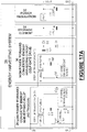
- FIG. 1 shows the FET family free.
- a JFET is the simplest form of Field Effect Transistor and can be used as an electronically-controlled switch or as a voltage-controlled resistance.
- FIG. 2 Here described is the behaviour based on an N Channel JFET as shown in Figure 2 .
- Recent attempts have been made utilizing a Depletion Mode MOSFETs or JFETs in combination with a step up transformer to harness ambient energy that provides voltages below 0.7 Volts. Due to the low IDSS and the relatively high RDS (On) although outputs of several volts can be achieved, the output power is limited due to the limited current.
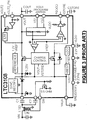
- One example is a prior art system comprising of an energy harvesting integrated circuit (IC) LTC1308 by Linear Technology Corporation of 1630 McCarthy Boulevard. Milpitas, CA 95035-7417 as shown in Figure 3 .
- the harvested energy from the ambient source is captured to charge a small capacitor to up to 3.3 Volts.
- the ambient source is from a Thermo Electric Generator (TEG) in the form of a Peltier module.
- TOG Thermo Electric Generator
- the key technology is the step up transformer of a ratio of 1:100 in combination with an N Channel Depletion Mode MOSFET within the LTC3108 integrated circuit which acts like an oscillator to charge a small
- the charger circuit is based on a Forward Converter design. Usually for a Forward Converter an external pulse stream is provided at the Gate of the FET. However, due to the low input voltage, as the N Channel Depletion Mode MOSFET is on at zero volts, when a low voltage is applied, the secondary steps it up by 100 to give around 2 Volts increasing the drain current until again there is an oscillation where the FET turns OFF and ON.
- the capacitor 'C2' is part of a resonant tank circuit between the inductance of the transformer secondary windings, and the input Gate Source capacitance of the FET. This is to allow the oscillating frequency to be towards the self-oscillating frequency of the transformer to allow it to perform at its optimum.
- the 2 volts or so is also then used as the output to charge the storage capacitor 'Cout' via the de-coupling capacitor 'C1' and the rectifier circuits in the LTC3108 IC.
- the de-coupling capacitor 'C1' in combination with the internal diode across the 'C1' terminal and ground of the LTC3108 is used to bring the voltage from the secondary windings positive as the transformer output is an alternating sinusoid on a zero volt axis.
- the internal rectification and decision making circuits of the LTC3108 decide when to charge the capacitor 'Cout' and send a signal to an external microprocessor to inform it that the capacitor is charged and hence it can send data.
- the device is asserted to have an RDS (On) of 0.5 ohms.
- the application of the device is limited to remote wireless sensor systems as the charged capacitor is then used as a power source to capture data from sensors, process through a microprocessor and send the data.
- FIG 4 shows using the LTC3108 for a heat based energy harvesting system for a remote wireless sensor application.
- a TEG outputs a voltage of less than 0.1 Volts.
- the charge time of the capacitor terminated at 'VOUT' based on the step up transformer ratio is shown in Figure 5 . It can be seen that any data transmission is therefore not instantaneous as the capacitor requires some time to charge first before it can then be used as a power source for the wireless sensor system.
- the energy harvesting solution provided by Linear Technology Inc. in the LTC3108 is deemed to be the industries best and coined the phrase 'The Missing Link for Energy Harvesting Applications'.
- the charger circuit arrangement using a Depletion Mode MOSFET or a JFET in combination with a step up transformer is common.
- the output power is limited.
- This solution is impressive as the processing is done using a single IC device.
- the IC is expensive, requires a specific type of step up transformer and requires that the system developer use their device which in turn provides a limited output power that is not instantaneous. It therefore would take hours as a larger capacitor would be needed to be charged so as to send larger amounts of data over a longer range for example.
- ECT310 by Enocean GmbH of Kolpingring 18a, D-82041 Oberhaching, Germany. This is a module containing discrete components and the same 1:100 ratio step up transformer, the LPR6235-752SMLB by Coilcraft Inc. of 1102 Silver Lake Road, Cary IL 60013, USA which is used for the LTC3108 example described in Figure 4 . It is used as a thermal energy powered energy harvester which works with a peltier module.
- the ECT310 can operate from 20 mV relating to a 2 Kelvin temperature difference provided by the Peltier module.
- the 20 mV operating voltage is also the same as the example described in the LTC3108 based system of Figure 4 .
- the ECT310 module is designed for use with wireless sensor networks and restricts use to only the Enocean radio protocol. To this end the ECT310 module can only be used with Enocean's own wireless sensor system such as the STM300 or STM 312 radio module.
- the Enocean radio module would wake up every 2 minutes to transmit a telegram which requires approximately 5 micro watts, (0.000005 watts) once the ECT310 module has charged a small capacitor between 3 to 5 Volts. Hence the power is limited for small bursts of data of only 5 microwatts every two minutes and not instantaneous data output which would require significantly greater power output.
- Zero Threshold MOSFETs They potentially have many advantages in energy harvesting applications due to their zero threshold voltage and hence can start operating without a need for a step up transformer. However, presently, they are depletion mode MOSFETS, therefore they would serve the same purpose as the JFET or standard Depletion Mode MOSFET in terms of power output. Their output is significantly less than Enhancement Mode MOSFETs due to their higher RDS.
- US.Pat. No. 2002074898 discloses a 'Self-powered wireless switch' powered by a piezo electric switch driving an RF transmitter.
- a paper written by Joseph A. Paradiso and Mark Feldmeier entitled 'A Compact, Wireless, Self-Powered Pushbutton Controller' shows the same circuit in more detail used for the application for an RF ID Tag.
- a piezo element is struck by way of a piezo electric switch which generates 2000 volts similar to a cigarette lighter.
- the output power is limited in that it can only charge a 4.4 ⁇ F (micro Farad) Capacitor to power an encoder and a RF transmitter to 3 Volts, and transmit a 12-bit digital code sequence for a limited 30 ms (Milliseconds).
- Graphs of the capacitor voltage after striking the piezo electric switch and the transmission are illustrated in Figure 7 .
- the ID tag application it is aimed for it has limitations due to the limited 12-bit digital code sequence (due to the frequency limitations and the 30 ms transmit time available) which means only 4096 codes can be obtained. These codes can only be programmed by hard wiring each of the encoders in 4096 separate units. The button also needs to be pressed to enable it to operate.
- thermoelectric energy harvesting device A further design of thermoelectric energy harvesting device is disclosed in Shuttleworth R et al: "Discrete, matched-load, step-up converter for 60-400 mV thermoelectric energy harvesting so", ELECTRONICS LETTERS, IEE STEVENAGE, GB, vol. 49, no. 11, 23 May 2013 (2013-05-23), pages 719-720, XP006044041 . It has what can be described as low and high power energy harvesting circuits but these are not independent of each other and cannot operate resonance-tuned. This device scavenges heat from boilers and hot water systems, not body heat. It needs 60mV to begin to operate and it is inefficient and bulky.
- the low power energy harvesting circuit is configured to operate at a lower power level than the high power energy harvesting circuit, driving or triggering the high power energy harvesting circuit for operation.
- the low power energy harvesting circuit is configured to operate at a power level that is at least ten times lower than that of the high power energy harvesting circuit and particularly preferably of the order of 100 times lower than that of the high power energy harvesting circuit.
- Each of the low power energy harvesting circuit and the high power energy harvesting circuit comprise at least one Field Effect Transistor (FET) respectively and the power level of each energy harvesting circuit may be assessed by the RDSon (Source Drain Resistance when switched ON) for the Field Effect Transistor (FET) in the respective energy harvesting circuit.
- FET Field Effect Transistor
- the RDSon for the FET of the low power energy harvesting circuit may be of the order of 1 Ohm. That of the high power energy harvesting circuit is of the order of 0.1 Ohms and below and preferably of the order of 0.005 Ohms or less.
- the electrical energy from the TEG is processed first via the low power energy harvesting circuit and then via the high power energy harvesting circuit.
- the transmitter may for example be a car key-fob, a part of a Remote Keyless Entry (RKE) System, a 'keyless go' an RFID tag or a person location tracker or a remote control.
- the transmitter itself can be RF, Infra-Red or Ultrasonic for example.
- the device does not require any batteries or charging up over time and can enable instantaneous transmission of data by way of the energy harnessed by the user's body heat.
- the device can be a single switch transmitter or can self-start automatically when a heat source is present allowing electrical energy to already be stored to power a multifunction remote control or an automatically powering a transmitter for a person location device or an ID Tag.
- the device can also harness energy from power sources less than 20mV as the user's hand may be cold for example when handling a key-fob remote control for example.
- the system preferably comprises a control system which is powered by the high power energy harvesting system.
- the system comprises a transmitter which is powered by the high power energy harvesting system.
- the system preferably comprises an Infra-Red, RF or Ultrasonic transducer.
- the device preferably has one or more Peltier modules as Thermo Electric Generators (TEG).
- TEG Thermo Electric Generator
- a Thermo Electric Generator (TEG) is suitably incorporated in an arm band or other wearable band to convert the heat from the user's body heat to electricity.
- the low power energy harvesting circuit comprises one or more Depletion Mode Field Effect Transistors, one or more Enhancement Mode Metal Oxide Semiconductor Field Effect Transistors and one or more step up transformers.
- the low power energy harvesting circuit suitably has one or more Depletion Mode Field Effect Transistors or one or more Junction Field Effect Transistors and one or more step up transformers to form an oscillator.
- the low power energy harvesting circuit comprises a step up transformer whose core is of a high relative permeability between 5000 and 20,000.
- the high power energy harvesting circuit comprises one or more Enhancement Mode Metal Oxide Semiconductor Field Effect Transistors and one or more of: a step up transformer; a fly-back transformer; and an inductor.
- the oscillator of the low power energy harvesting circuit suitably drives the Enhancement Mode Metal Oxide Semiconductor Field Effect Transistor of the high power energy harvesting circuit.
- the Enhancement Mode Metal Oxide Semiconductor Field Effect Transistor can switch a said step up transformer to serve as a forward converter and/or said fly-back transformer to serve as a fly-back converter and/ or said inductor to serve as a boost converter
- the high power energy harvesting circuit comprises a step up transformer whose core is of a high relative permeability between 5000 and 20,000.
- the high power energy harvesting circuit comprises a fly-back transformer whose core is of a high relative permeability of at least 20,000.
- the high power energy harvesting circuit comprises an inductor whose core is of a high relative permeability of at least 80,000.
- the high relative permeability core used is Nanoperm(RTM) nanocrystalline magnetic alloy or Metglas(RTM) amorphous magnetic alloy.
- the system preferably has a high power energy harvesting system comprising a step up transformer and an Enhancement Mode MOSFET configured as a 'Forward Converter' which is triggered by the either a switch or a low power energy harvesting system. Once triggered, the high power energy harvesting system then can function off its own accord without the need for the switch or the low power energy harvesting system.
- the system has a high power energy harvesting system comprising a step up transformer and an Enhancement Mode MOSFET configured as a 'Forward Converter' or a 'Flyback Converter' with the gate of the Enhancement Mode MOSFET driven by the low power energy harvesting system.
- the system has a high power energy harvesting system comprising an inductor and an Enhancement Mode MOSFET configured in as a 'Boost Converter' with the gate of the Enhancement Mode MOSFET driven by the low power energy harvesting system.
- the Low Power Energy Harvesting circuit preferably also comprises one or more Enhancement Mode Metal Oxide Field Effect Transistors. A single one may be used to trigger the Enhancement Mode Metal Oxide Field Effect Transistor within the High Power Energy Harvesting circuit which switches a step up transformer for a forward converter.
- One or more further Enhancement Mode Metal Oxide Field Effect Transistor(s) within the Low Power Energy Harvesting circuit is/are used to create a square wave oscillator. This may have adjustable pulse width and duty cycle above 50% with output voltages above 1 Volt peak to peak.
- the Low Power Energy Harvesting circuit which may comprise a Depletion Mode Field Effect Transistor and step up transformer forming an oscillator, is suitably used as a forward converter. This may charge a small capacitor to voltages above 1 Volt DC (Direct Current) to provide a power source for the square wave oscillator.
- the square wave oscillator within the Low Power Energy Harvesting circuit may then be used to drive an Enhancement Mode Metal Oxide Field Effect Transistor within the High Power Energy Harvesting circuit which switches a flyback transformer for a flyback converter or for an inductor for a boost converter.
- the output may then be stored in a Storage Element.
- the Storage Element may be in the form of a capacitor.
- the storage element is chosen to meet the energy and voltage requirements of the application. This may then be regulated by a Power Regulation circuit to of the Energy Harvesting system to ensure the output voltage of the Energy Harvesting system is stable for the desired application.
- the energy harvesting system itself has a number of unique features and is highly sensitive and efficient and may have applications other than as a wireless transmitter.
- a Thermo Electric Generator in the form of a Peltier module sized to fit in the arm band (typically 40 mm X 40 mm by 3 mm) would only generate typically about 0.1 Volt based on the from the temperature difference created by the users body heat on one side.
- the TEG has very low resistance from less than 1 Ohm to a few Ohms. This means that although it can generate less than 0.1 volt, the output current is quite high.
- Using the enhanced energy harvesting system of the present invention it is therefore possible to utilise this to generate enough power to directly power or charge the battery within an MP3 player or mobile phone.
- a mobile phone or mp3 player arm band may be used as the wearable band. It could be also incorporated inside the housing of various portable electrical devices such as mobile phones, MP3 players. When housed within an MP3 player or mobile phone, using a Thermo Electric Generator, the electrical energy could also be drawn from the heat while in the users pocket or when held in their hand. Another example use is to power a torch which could either be handheld type or a head worn type. Here the heat from the users head can be harvested. This type of head torch could be used by miners for example where a power point to charge a conventional rechargeable battery powered version would not be available underground for example.
- the present invention addresses many of the afore-mentioned short-comings of the prior art. It has utility inter alia for RFID tags and personal location trackers and enhances the perceived 'portability' of portable electronic devices in general.
- the present invention makes use of zero carbon components that are easily and cheaply obtainable within its design and recyclable components that are easily and freely obtainable.
- the present invention still further provides significant improvements to an existing Integrated Circuit based energy harvesting system deemed the industries best and provides a new Energy Harvesting Integrated Circuit.
- the present invention further provides improved Energy Harvesting Systems in general and can be used in applications for powering or charging batteries of portable products such as MP3 players and mobile phones by body heat.
- a summary of some primary benefits of the system of the present invention include but are not limited to: i) Zero Carbon (no batteries required); ii) Zero maintenance (no moving parts for the energy harvesting system - only standard switches used and only if required, e.g. for RF and Infra-Red remote controllers); iii) Compensates for variations or intermittent availability of voltage of energy source (such as cold hands, or unit on table before user touches it); iv) High power output; v) Instantaneous power in ⁇ 1 second from touch of users body, e.g.
- Power limitations - Limited to 20 mV input voltage - Power is limited by the RDS(On) of the Depletion Mode N channel MOSFET - Application limited to remote wireless sensor data capture systems due to non-instantaneous power - Expensive (several pounds sterling) and SMT technology only
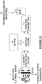
- FIG 8 shows a simplified system overview of the Body Heat Powered Wireless Transmitter of the present invention.
- the user '1' may hold the unit, have it in their pocket or have it worn on their wrist or strapped to their arm.
- the heat is captured by the Thermo Electric Generator '2' by way of the 'Seebeck' effect.
- the preferred unit for the heat capture is a 'Peltier' unit.
- the Seebeck effect is the conversion of temperature differences into voltage.
- one side of the Peltier unit is in contact with the human body, while the other is in contact with the system enclosure.
- the temperature difference between the body heat (37C) and the other side will then produce a voltage. Higher voltages are obtained if the other side is a metal enclosure or heatsink.
- This is then processed via the energy harvesting system '3' to power the desired processing system '4'.
- This essentially is a controller or decision making system which takes an input, processes it and gives an output.
- the term 'Processing System' in the context of this document can therefore be any but not limited to the control system part of a keyfob remote controller, a Remote Keyless Entry (RKE) System or an Infra-Red remote controller for example.
- This 'data' is then transmitted via the wireless transmitter '5' which converts the 'data' steam to a useable format to transmit using the desired transmission medium '6'. For example if '4' was en encoder for an ID tagging system, the frequency of the data may be 3 KHz.
- the key input control could be a switch for a RF keyfob remote or Remote Keyless Entry (RKE) System, a keypad (Infra-Red remote), an encoded code (RF ID Tag), a co-ordinate (Person Location System), or a sensor (Wireless Data Capture System).
- RKE Remote Keyless Entry
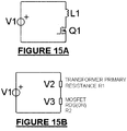
- FIG 15a shows a simplified representation of a charger circuit showing the voltage source, 'V1', an inductor, the primary side of a step up transformer, 'L1', and a FET, 'Q1'.
- the voltage source 'V1' is of a Themo Electric Generator (TEG).
- 'R2' is represented as the DC resistance of an inductor or the primary side of a step up transformer.
- 'R3' represents the On resistance of the FET, RDS(On).
- the output voltage is stepped up using a step up transformer to boost the low 20 mV to 2 Volts using a 1:100 turn step up transformer in combination with a Depletion Mode N Channel MOSFET.
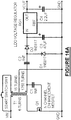
- FIG. 16a and 16b both are such examples using an N Channel Enhancement Mode MOSFET with an RDS(On) of 0.005 Ohms together with a step up transformer.
- the step up transformers have been taken from a popular disposable photoflash camera.
- the principle operation of a photoflash camera, in particularly a disposable one is such that a 1.5 Volt AA or AAA battery is used to charge a typically 100 uF (Micro Farad) capacitor to 300 Volts. This is then discharged into a high voltage Xenon Flash Tube to create the high intensity light for the flash.
- the step up transformer has a turns ratio of approximately 1:300 and serves to boost the voltage from approximately 1 volt to 300 volts to charge the capacitor in a forward converter configuration. They are compact in size in that they or less than 1 square cm and can therefore be housed within a keyfob transmitter enclosure together with an encoder and transmitter.
- Figure 16a comprises of a disposable photoflash camera transformer with two primary windings and one secondary winding. Closing the switch 'SW1' will boost the secondary voltage of the transformer momentarily by '116' by the turns ratio 1750/15. This in turn will allow the voltage at the gate of the N Channel Enhancement Mode MOSFET to be greater than 2 Volts allow the input source voltage to be presented across the other primary winding (6 Turns). This in turn will be boosted by 291.66 (1750/6) times and switch the gate of the MOSFET again. The circuit will then oscillate once the switch is released.
- F Frequency in Hz
- L Inductance (of the secondary windings of the transformer) in Henries
- C Total series capacitance of the tank capacitor 'C1' and MOSFET input capacitance in Farads.
- 'C2' is a de-coupling capacitor and together with 'D1' make the sinusoidal waveform from being centered on the zero volts axis to make the waveform positive only. 'D2' then acts as a rectifier charging the capacitor 'C3' on the positive peaks of the waveform.
- 'RG1' is a low dropout regulator to provide a constant supply voltage and 'C4' is used to remove any ripples in the DC supply out voltage.
- Figure 16b is another example. Here it comprises of a disposable photoflash camera transformer with one primary winding and one secondary winding. Closing the switch SW1 will allow the input source voltage to be presented across the primary winding (6 Turns). This in turn will be boosted by 291.66 (1750/6) times and switch the gate of the N Channel Enhancement Mode MOSFET again. The circuit will then oscillate once the switch is released.
- the resonant tank circuit operates in the same manner as the one described in Figure 16a together with the rectification and voltage regulation circuits.
- the system '28' comprises of a Low Power '29' and a High Power Energy Harvesting circuit '30'.
- the low power energy harvesting circuit '29' takes advantage of a Depletion Mode FET (always 'ON') together with the advantages of high input impedance of FETs in general.
- 'Q1' is a N Channel JFET, part of the Depletion Mode FET family. At zero volts it is 'ON' and allows a small amount of current through its Drain and Source terminals causing the input source voltage to be presented across the primary winding (6 Turns). This in turn will be boosted by 291.66 (1750/6) times and switch the gate of the JFET 'Q1' 'OFF' by a negative voltage swing equalling its Turn Off voltage of -2 Volts to - 6 Volts.
- the circuit will then oscillate by way of a sinusoidal waveform swing of +/- 6 Volts.
- the capacitor 'C1' forms part of a resonant tank circuit between the inductance of the transformer secondary windings, and the input Gate Source capacitance of the JFET. This is to allow the oscillating frequency to be towards the self-oscillating frequency of the transformer to allow it to perform at its optimum.
- N Channel JFET 'Q1' used is a J106 which has an RDS(On) of 6 Ohms and hence although the voltage swings between -6 and 6 Volts, it is of a low current.
- this will be sufficient to turn on the high power circuit by way of the N Channel Enhancement Mode MOSFET, 'Q2' which has an RDS(On) of 0.005 Ohms and a Turn On voltage of 2 Volts but a very high impedance of tens of millions of ohms which makes it very easy to drive. This will be done instantaneously, which is the moment the voltage to the gate of Q2 is above 2 Volts.
- Waveform '1' is across the Drain and Source of a High Power (100 Amp) N Channel Enhancement Mode MOSFET whose RDS (ON) is 0.005 Ohms (5 milli Ohms).
- Waveform '2' is across the output of a photoflash transformer 'T2' showing a stepped up voltage sinewave. This re-triggers the MOSFET 'Q3' and charges the capacitor 'C4' of the storage element '31'.
- Figure 18 shows an arrangement using the same photoflash disposable camera transformers and operation is the same as that described in Figure 17a .
- the Low Power Forward Converter '34' creates pulses to switch the N Channel Enhancement Mode MOSFET 'Q2' ON and OFF in the High Power Forward Converter Circuit '35'.
- the secondary windings of transformer 'T2' step the input voltage 'Vin' up by 291.66 (1750/6) and charges the capacitor 'C4' of the storage element '36'.
- the Low Power Forward Converter '34' frequency output is set to that of the resonant frequency of the transformer 'T2' in the High Power Forward Converter '35'. This is to allow the use of a very wide range of MOSFETs and transformers to be used in the High Power Forward Converter '35'. This is because some MOSFETs with very low RDS(On) may have a high input Gate Source capacitance hence the system can still operate at the transformer 'T2' resonant frequency for optimum power output.
- Coupling is the factor of which how much the energy is transferred from the primary to the secondary side of the transformer windings and is a maximum of 1 (unity).
- the photoflash camera transformer used in the forward converters '29' and '30' in Figure 17a as well as '34' and '35' in Figure 18 use a ferrite core transformer and required 6 primary turns and therefore 1750 secondary turns to achieve a strong coupling to provide a 291.66 factor voltage boost.
- the 6 primary turns therefore provide sufficient inductance and therefore magnetic flux.
- the higher the inductance the lower the frequency of operation. Having less turns would therefore increase the frequency and may increase losses and cause core saturation at high currents using the ferrite core.
- Ferrite cores have a relative permeability ' ⁇ r ' of around 640 which is useful for a step up transformer. This is the ability of a material to support the formation of a magnetic field within itself. In other words, it is the degree of magnetization that a material obtains in response to an applied magnetic field. Therefore a good magnetic core material must have high relative permeability. However, the primary inductance per turn can be increased using a core material of higher relative permeability.
- the term high relative permeability can be referred to a value that is 10 or 100 times or greater than that of Ferrite and is achieved by using such materials as Nanoperm(RTM) nanocrystalline magnetic alloy or Metglas(RTM) amorphous magnetic alloy.
- the inductance will accordingly increase by 10 to 100 times and also allow smaller cores to be used.
- Nanoperm(RTM) nanocrystalline or Metglas(RTM) amorphous magnetic alloy in particular also reduce core losses and core saturation at high currents.
- a single turn can be used for the primary rather than 6 and hence the secondary turns can be reduced by the same factor to give the same voltage boost while achieving greater power and efficiency due to the reduced DC (Direct Current) resistance and therefore greater output current.
- DC Direct Current
- the transformer core size can be reduced accordingly while still allowing thicker wires for the windings for higher currents therefore and power output than the original core;
- High Power RF (Radio Frequency) N Channel Enhancement Mode MOSFETs can be used. They have a very low RDS(ON) and also-a very low input source drain capacitance. However, presently, they are more expensive. Hence they have not been chosen as the preferred standard devices as part of the objective of this invention is low cost.
- the step up transformer cores in these forward converter circuits are of high relative permeability.
- a high relative permeability of between 5000 and 20,000 is particularly preferred for the Low Power Energy Harvesting Circuits '29' in Figure 17a , '34' in Figure 18 and the 'Self Triggered' High Power Energy Harvesting Circuit '30' of Figure 17a .
- a high relative permeability of 20,000 is particularly preferred for the 'External Gate Triggered' High Power Energy Harvesting Circuit '35' of Figure 18 .
- Preferred examples of high permeability materials are Nanoperm(RTM) nanocrystalline magnetic alloy or Metglas(RTM) amorphous magnetic alloy.
- transformers may still be the same size as the disposible camera transformer allowing a versatile small form factor while giving significant power and efficiency gains and enabling the circuit of the present invention to operate effectively for the proposed applications. This is described in more detail in the boost converter design proposal of Figure 20a described in this document.
- This type of converter involves using a flyback transformer.
- a flyback transformer is designed not just to transfer energy, but also to store it for a significant fraction of the switching period. The current does not flow simultaneously in primary and secondary (output) windings of the transformer. Because of this the flyback transformer is really a coupled inductor rather than a classical transformer, in which currents do flow simultaneously in all magnetically coupled windings.
- a flyback transformer was invented as a means to control the horizontal movement of the electron beam in a television cathode ray tube (CRT) and generates very high voltages in the order of 50 KV (Thousand Volts). Here it is referred to as the Line Output Transformer (LOPT).
- LOPT Line Output Transformer
- miniature ones are used for SMPs (Switched Mode Power supplies).
- the primary side of the transformer is used as an inductor.
- a transformer with a core such as ferrite is used which has a higher relative permeability than the laminations of a conventional transformer such as a mains or audio one. This way it is possible to get high inductance on the primary side with a lower number of windings.
- the secondary is then used to step the voltage up and it is possible to have additional windings for applications such as TV sets.
- the flyback converter works on the principle of charging the primary side of the transformer to store energy within the transformer core. Then the energy released when power is removed from the primary side of the transformer and the magnetic field within the core collapses.
- V LdI / dt
- I Current
- t duration of time when power is removed from the inductor.
- Figure 19a shows an arrangement using the same photoflash disposable camera transformers.
- the Low Power Forward Converter '39' creates pulses to switch the N Channel Enhancement Mode MOSFET 'Q2' in the High Power Flyback Circuit '40'.
- the black dots on the transformer shows the starting of the windings.
- you will notice the actual polarities between primary and secondary are reversed relative to 'GND'.
- the gate to 'Q2' is high, the primary side of the transformer 'T3' is charged. When it goes low, the energy from the primary side is released. At this point, the secondary windings step this voltage up and charge the capacitor 'C4' of the storage element '41'.
- the Low Power Forward Converter '39' serves as an oscillator whose frequency is optimised to meet the charge and discharge times of the inductance of the primary winding of flyback transformer 'T3' of the High Power Flyback Circuit '40'.
- the output of the Low Power Forward Converter '39' and the High Power Flyback circuit '40' are not 'High' at the same time but rather during opposite times hence less drain on the input power supply; ii) The Back-EMF generated is a factor of the current as well as the inductance of the primary side of the flyback transformer 'T3', hence a low voltage high current source such as a TEG together with a low RDS(On) of 0.005 Ohms N Channel Enhancement Mode MOSFET 'Q2' are advantageous even at very low voltages; iii) Due to the high primary current, high voltage peaks are possible with a low number of secondary transformer windings for the flyback transformer 'T3'; iv) A reduced number of secondary windings of 'T3' means the output current will be high and hence a high output power is possible.
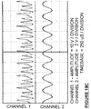
- Figure 19b shows the behaviour of this circuit comparing the behaviour across the primary windings of the flyback transformer 'T3' with the 'Gate' drive of the N Channel Enhancement Mode MOSFET 'Q2'.
- Waveform '2' shows the output of the Low Power Energy Harvesting Circuit Driving the 'Gate' of 'Q2' which is also a High Power (100 Amp) N Channel Enhancement Mode MOSFET whose RDS (ON) is of 0.005 Ohms (5 milli Ohms).
- Waveform '1' shows the primary windings of the Flyback Transformer 'T3' which releases its stored energy once the Gate signal is low. You will notice that although the supply voltage is less than 50mV, the released energy voltage is 3 times the amount. This means less turns are required for the step up and hence higher power output.
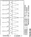
- Figure 19c compares the behaviour across the secondary windings of the flyback transformer 'T3', waveform 1' with the 'Gate' drive of the N Channel Enhancement Mode MOSFET 'Q2', waveform '2'. It can be seen that the secondary winding of 'T3' show a peak voltage of almost 20 Volts.
- V LdI / dt
- V the Back-EMF generated in Volts
- L Inductance
- I Current
- t duration of time when power is removed from the inductor.
- Ferrite cores have a relative permeability ' ⁇ r ' of around 640 which is useful for a step up transformer. This is the ability of a material to support the formation of a magnetic field within itself. In other words, it is the degree of magnetization that a material obtains in response to an applied magnetic field. Therefore a good magnetic core material must have high relative permeability. However, the primary inductance per turn can be increased using a core material of higher relative permeability.
- the term high relative permeability can be referred to a value that is 10 or 100 times or greater than that of Ferrite and is achieved by using such materials as Nanoperm(RTM) nanocrystalline magnetic alloy or Metglas(RTM) amorphous magnetic alloy.
- the inductance will accordingly increase by 10 to 100 times and also allow smaller cores to be used. This also means that the number of turns is reduced for the same inductance and hence reducing DC resistance of the wire. In turn, thicker wire could be used to reduce DC resistance further. This will give rise to higher currents hence greater Back-EMF as well. It is also possible to have multiple wires connected and wound in parallel for high frequency due to the 'skin effect' due to the extra space available now. High permeability cores also saturate at higher currents. Saturation is when the magnetic flux drops and causes a decrease in the inductance. This particularly prevalent at high frequencies and hence larger sized cores are needed. However, using high relative permeability cores such as Nanoperm(RTM) nanocrystalline magnetic alloy or Metglas(RTM) amorphous magnetic alloy can prevent high current saturation and decrease losses.
- high relative permeability cores such as Nanoperm(RTM) nanocrystalline magnetic alloy or Metglas(RTM) amorphous magnetic alloy can prevent high current saturation and decrease losses
- the secondary winding wire thickness can also be increased by 360 and therefore the 1750/6 turns ratio flyback transformer 'T3' of the High Power Flyback Circuit '40' can therefore be replaced with that of a high relative permeability core material of 20,000 with only a 1 turn primary and 5 turn secondary winding providing 2 Volts output with high current.
- TOG Thermo Electric Generator
- the 3 turns primary is proposed instead of 1 to create a large proportion of the Back-EMF from the inductance as well as the current as observed in Eq. 4. This is to compensate for variation of the available current from the range of TEGs presently available on the market as well as variation of the available body heat from the user.
- core materials of a higher relative permeability than 20,000 are possible for the transformer in the flyback converter configuration as it does not operate at a resonant frequency but rather it is based on the charge and discharge times of the primary winding inductance which is a factor of the input current.
- Nanoperm(RTM) nanocrystalline magnetic alloy or Metglas(RTM) amorphous magnetic alloy will also prevent high frequency saturation at high currents.
- the flyback transformer core be of high relative permeability, i.e. at least 20,000.
- Preferred examples are Nanoperm(RTM) nanocrystalline magnetic alloy or Metglas(RTM) amorphous magnetic alloy. These transformers may still be the same size as the disposable camera transformer allowing a versatile small form factor while giving significant power and efficiency gains and enabling the circuit of the present invention to operate effectively for the proposed applications.
- a boost converter is a simplified flyback converter whereby only an inductor is used and there is not step up of the voltage. So the behaviour of operation is the same.
- the first three observation points for the flyback topology also apply here. As there is no secondary winding, the current remains the same (that is, it is not stepped down).
- a high relative permeability core will provide: i) High inductance with a low number of turns and therefore high back EMF; ii) Lower saturation at high current; and iii) Lower saturation at high frequency.
- Thick wires for the windings can be used due to the reduced number of turns to reduce DC resistance or multiple wires in parallel for high frequency due to 'skin effect'.
- Output power is high due to higher frequency capability, high current and voltages above the threshold voltage (0.7 Volts or more) of conventional semiconductor devices
- Ferrite cores have a relative permeability ' ⁇ r ' of around 640 and are useful in inductors and for the application of boost converter configurations.
- a good magnetic core material must have high relative permeability. This is the ability of a material to support the formation of a magnetic field within itself. In other words, it is the degree of magnetization that a material obtains in response to an applied magnetic field. However, the primary inductance per turn can be increased using a core material of higher relative permeability.
- the term high relative permeability can be referred to a value that is 10 or 100 times or greater than that of Ferrite and is achieved by using such materials as Nanoperm(RTM) nanocrystalline magnetic alloy or Metglas(RTM) amorphous magnetic alloy.
- Nanoperm(RTM) nanocrystalline magnetic alloy or Metglas(RTM) amorphous magnetic alloy can prevent high current saturation and decrease losses.
- Metglas(RTM) amorphous 2714A alloy has the highest relative permeability which is starting to be introduced into the industry.
- a typical core made of this material could be MP3210P4AF by Manz Electronic Systeme OHG. With this material, even higher output power is achievable at higher frequency without saturation.
- Figure 20a shows an energy harvesting system '43' containing a high power boost converter circuit '45' with an inductor, 'L1' wound on a Nanoperm(RTM) M-102 high permeability Nanocrystalline Soft Magnetic Alloy core by Magnetec GmbH. It has a relative permeability of 90,000.
- the inductor 'L1' has 40 windings on SWG 28 copper enamelled wire. This gives an inductance 141 mH (milli Henries) and a measured DC resistance of less than 0.1 Ohms.
- the Low Power Forward Converter '44' serves as an oscillator whose frequency is optimised to meet the charge and discharge times of the inductor 'L1' of the High Power boost converter Circuit '44'
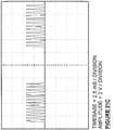
- Figure 20b compares the behaviour across the inductor 'L1', waveform '1' with the 'Gate' drive of the N Channel Enhancement Mode MOSFET 'Q2', waveform '2'. It can be observed that the inductor releases its stored energy when the 'Gate' is 'Off' giving pulses of short duration. However, they have a peak voltage of over 1 Volt even with a supply voltage of less than 50 mV. This means that it is possible to charge a capacitor via the silicon diode 'D2' whose nominal forward voltage drop is 0.7 Volts. That is, the diode needs more than 0.7 volts to operate.
- the inductor winding resistance is less than 0.1 ohm and in combination with the low RDS (On) of the N Channel Enhancement Mode MOSFET of 5 mOhms (5 milli Ohms or 0.005 Ohms) means that although the pulse is around 1 Volt, the current is high and hence it is possible to charge large capacitors quickly.
- core materials of a higher relative permeability than 90,000 are possible for the described inductor in the boost converter configuration as it does not operate at a resonant frequency but rather it is based on the charge and discharge times of the primary winding inductance which is a factor of the input current.
- Using Nanoperm(RTM) nanocrystalline magnetic alloy or Metglas(RTM) amorphous magnetic alloy will also prevent high frequency saturation at high currents.
- the inductor core be of high relative permeability of at least 80,000.
- Preferred examples are Nanoperm(RTM) nanocrystalline magnetic alloy or Metglas(RTM) amorphous magnetic alloy.
- the inductor may still be compact in size for portable or small form factor applications while giving significant power and efficiency gains and enabling the circuit of the present invention to operate effectively for the proposed applications.
- Figure 21a shows a real tested body heat powered RF 433 MHz transmitter which can be used as a 4-way remote control or a RFID tag.
- the complete system is housed in a standard keyfob remote control enclosure.
- the heat is drawn from a 20 mm x 20 mm TEG, '48', giving a voltage output from less than 20 mV to 50 mV.
- This energy harvesting system, '49' is the automatically starting, self-trigger circuit of Figure 17a .
- the circuit charges a 47 ⁇ F (micro Farad) capacitor, 50 to above 5 volts which then maintained at 5 volts by the internal voltage regular of '49'.
- the key components in the energy harvesting system, '49' are 'Q1', the N Channel JFET, part number J106, a standard cheaply available component costing a few pence.
- the N Channel Enhancement Mode MOSFETs, 'Q2' and 'Q3' have a very low RDS(On) of 0.005 Ohms (5 Milli Ohms) but are standard cheaply available components costing less than one 1 pound sterling.
- the same 12-bit Holtek HT12E encoder '51' is used.
- the frequency of the encoder is set by R2 which is 500 KOhms giving a frequency of 6 KHz.
- the encoder has eight address pins, and four pins which can be used either for address or data.
- the address state switches, '51' for A0 to A7, are left open, while AD6 to AD11 are pushbuttons, '53' which can be used for a 4-way remote control.
- SW1 is switched to VSS upon transmission.
- the transmitter '55' is a typical keyfob or Remote Keyless Entry (RKE) System RF remote frequency type at 433 MHz, part number AM-RT4-433 by RF Solutions Ltd.
- RKE Remote Keyless Entry
- a special configuration is made using the diodes, D3 to D10 which means that the VSS, the transmit enable of the encoder '49', and the VSS of the transmitter '55' will not be connected to the GND terminal of the energy harvesting circuit '49' unless any of the switches SW1 to SW2 are depressed.
- the VSS rail '54' will be connected to the GND rail of '49'. This means that no power will be drawn from the energy stored in the capacitor '50' until any of the switches SW1 to SW2 are depressed.
- the storage capacitor '50' also serves as a buffer so that if there is no more heat present on the TEG, '48', data can be transmitted using the energy stored in it.
- a 433 MHz receiver '56', part number AM-RT5-433 by RF Solutions Ltd is placed 10 metres away and the waveform observed by an oscilloscope '57'.
- the receiver '56' is powered by a 4.5 Volt source consisting of three 'AA' 1.5 Volt batteries wired in series.
- Figure 21b shows the transmission when switch 'SW1' is pressed once the storage capacitor '49' is charged to 5 Volts and there is no longer any heat supplied to the TEG '48'. It can be seen that several pulse streams are received even though the storage capacitor '49' is a small value of only 47 ⁇ F (micro Farads).
- Figure 21c shows that the correct 12-bit sequences have transmitted several times. If heat is continuously available by the user, than the pulse streams would continuously be transmitted as long as the switch 'SW1' was pressed. The range would also be improved to more than 10 metres.
- GSM Global Satellite Monitoring
- GPS Global Positioning System
- the system advantageously has a capacitor and voltage level switch.
- the storage system is charged to a specified voltage to the person location system power requirements. If and only then is power from the storage capacitor is applied to it.
- the advantage is that the person location system consumes zero power until there is enough power to drive it. This is unlike existing battery powered systems where there is a microprocessor in 'Sleep Mode' which consumes some power until it is awakened to send the burst transmission.
- Figure 22 shows a Voltage Level switch based on an N Channel Enhancement Mode MOSFET (a), and a P Channel Enhancement Mode MOSFET (b).
- the MOSFETs are chosen to have a threshold voltage that of the voltage requirements of the person location system.
- Figure 23 shows the Body Heat Powered Person Location Device.
- the complete system can be housed within a wristband type enclosure.
- the heat is drawn from a 20 mm x 20 mm TEG, '58', giving a voltage output from less than 20 mV to 50 mV.
- This energy harvesting system, '61' is the automatically starting, self-trigger circuit of Figure 17a .
- the circuit charges a capacitor, '59' which is then maintained at a constant voltage by the internal voltage regular '60' to that of the person location system '63' and transmitter '64' system.
- the transmitter is integrated as part of the person location system as a whole.
- the storage capacitor '59' is chosen such that it has the energy requirements of the person location system.
- the voltage level switch '62' then only powers the person location system '63' and transmitter '64' when the desired voltage has been reached by the storage capacitor '59'.
- the voltage level switch N Channel Enhancement Mode MOSFET has a very low RDS(On) in the order of a few Milli Ohms (typically 0.005 Ohms).
- FIG. 24 shows the Infra-Red TV remote control connected to a preferred embodiment of a body heat powered energy harvesting system '68' and a voltage level switch '69' to provide it with a power source other than the batteries.
- the complete system can be housed within the battery compartment of the TV remote control.
- a TEG is then attached to the back of the TV remote control. When the user holds the TV remote control unit in their palm, heat is drawn and converted to electricity.
- the heat is drawn from a 20 mm x 20 mm TEG, '65', giving a voltage output from less than 20 mV to 50 mV.
- This energy harvesting system, '68' is the automatically starting, self-trigger circuit of Figure 17a .
- the circuit charges a capacitor, '66' which is then maintained at a constant voltage of 3 Volts by the internal voltage regular '67' to that of the Infra-Red TV Remote Control '70' supply voltage.
- the storage capacitor '66' is chosen such that it has the energy requirements of the Infra-Red TV Remote Control.
- a 47 ⁇ F (Micro Farad) capacitor charged to 3 Volts provides enough power to allow the desired signal strength and length of pulse stream to be detected by the TV receiver for 10 metres.
- the voltage level switch '69' then only powers the Infra-Red TV Remote Control '70' when 3 Volts has been reached by the storage capacitor '66'.
- the voltage level switch N Channel Enhancement Mode MOSFET '69' has a very low RDS(On) in the order of a few Milli Ohms (typically 0.005 Ohms). Typically, it takes less than a second to charge the 47 ⁇ F capacitor to the desired voltage. Once charged, the user does not need to provide heat to the TEG on the back of the remote control unit.
- a 40 mm x 40 mm TEG can provide a typical voltage greater than 50 mV with an internal resistance of 1 Ohm to still provide a high enough power in the proposed energy harvesting system '68' in Figure 24 .
- the 47 ⁇ F capacitor storage capacitor '66' used in this example is a conservative value in that it can be used to power the remote control once there is no more heat from the users hand applied to the TEG. If the user is still touching the TEG once the storage capacitor '66' is charged then multiple button presses can be made. It is also possible to use a larger value capacitor for more power and hence a longer range can be obtained.
- the invention therefore advantageously proposes HCS365 KEELOQ® Code Hopping Encoder by Microchip Technology Inc. designed for Remote Keyless Entry (RKE) and secure remote control systems, which incorporates high security and a small package outline.
- RKE Remote Keyless Entry
- KEELOQ® Cipher Keyfob transmitter and RKE systems based on the KEELOQ® Cipher are widely used by popular car manufacturers and secure entry systems.
- a 60-bit seed KEELOQ® Cipher provides the maximum security level.
- the length of the transmission eliminates the threat of code scanning and code grabbing access techniques.
- the invention advantageously proposes configuring the HCS365 Encoder to a 60-bit seed KEELOQ® Cipher which it is designed to provide for maximum security. This can be used inter alia for the following applications: i) RFID Tag; ii) Car Keyfob Transmitter; and iii) Remote Keyless Entry System (RKE).
- RFID Tag ii)
- Car Keyfob Transmitter iii)
- RKE Remote Keyless Entry System
- Figure 25 shows an embodiment of a Body Heat Powered RF Transmitter based on the HCS365 KEELOQ® Code Hopping Encoder.
- a single push button can be used for an RFID Tag or multiple ones 'B0 to B3' for a Keyfob transmitter or RKE system.
- the HCS365 KEELOQ® Code Hopping Encoder '76' and the RF transmitter '77' connected to a preferred embodiment of a body heat powered energy harvesting system '74' and a voltage level switch '75' to provide it with a power source other than a coin cell battery.
- the complete system can be housed within the keyfob enclosure.
- a TEG is then attached to the back of the enclosure. When the user holds the keyfob in their palm, heat is drawn and converted to electricity.
- the heat is drawn from a 20 mm x 20 mm TEG, '71', giving a voltage output from less than 20 mV to 50 mV.
- This energy harvesting system, '74' is the automatically starting, self-trigger circuit of Figure 17a .
- the circuit charges a capacitor, '72' which is then maintained at a constant voltage of 3 Volts by the internal voltage regular '73' to that of the HCS365 KEELOQ® Code Hopping Encoder '76' and the AM-RT4-433 by RF Solutions Ltd 433 MHz RF transmitter '77' supply voltage.
- the storage capacitor '72' is chosen such that it has the energy requirements of the HCS365 KEELOQ® Code Hopping Encoder '76' and the RF transmitter '77'.
- a 47 ⁇ F (Micro Farad) capacitor charged to 3 Volts provides enough power to allow the desired signal strength and length of pulse stream to be detected by the receiver for 10 metres.
- the voltage level switch '75' then only powers the HCS365 KEELOQ® Code Hopping Encoder '76' and the AM-RT4-433 by RF Solutions Ltd 433 MHz RF transmitter '77' when 3 Volts has been reached by the storage capacitor '72'.
- the voltage level switch N Channel Enhancement Mode MOSFET '75' has a very low RDS(On) in the order of a few Milli Ohms (typically 0.005 Ohms). Typically, it takes less than a second to charge the 47 ⁇ F capacitor to the desired voltage. Once charged, the user does not need to provide heat to the TEG on the back of the keyfob remote control unit.
- the 47 ⁇ F capacitor storage capacitor '72' used in this example is a conservative value in that it can be used to power the RF transmitter once there is no more heat from the users hand applied to the TEG. If the user is still touching the TEG once the storage capacitor '72' is charged then multiple button presses can be made. It is also possible to use a larger value capacitor for more power and hence a longer range can be obtained and a larger data code word than the one provided by the HCS365 KEELOQ® Code Hopping Encoder '76' for further security.
- the HCS365 combines a hopping code generated by a nonlinear encryption algorithm, a serial number, and status bits to create a secure transmission code.
- the length of the transmission eliminates the threat of code scanning and code grabbing access techniques.
- the HCS365 has a built-in small EEPROM (Electrically Erasable Programmable Read-Only Memory) array which is loaded with several parameters before use; most often programmed by the manufacturer at the time of production. The most important of these are: i) A serial number, typically unique for every encoder; ii) A crypt key; and iii) an initial synchronization value.
- EEPROM Electrically Erasable Programmable Read-Only Memory
- Figure 25b shows how the key values in EEPROM are used in the encoder.
- the 32-bit hopping code is combined with the button information and serial number to form the code word transmitted to the receiver.
- a receiver may use any type of controller as a decoder. Typically, it is a microcontroller with compatible firmware that allows the decoder to operate in conjunction with a HCS365 based transmitter.
- a transmitter is first 'learned' by the receiver before its use is allowed in the system. Learning includes calculating the transmitter's appropriate crypt key, decrypting the received hopping code, storing the serial number, storing the synchronization counter value, and storing the crypt key in the EEPROM.
- the HC365 encoder can be configured to various code word formats to suit the application by using the four buttons 'B0 to B3' to program the built in EEPROM prior to use. It can provide a data word length giving up to 69-bits per data transmission.
- Figure 25c shows a table of a configuration of the HCS365 encoder such that it can provide 32-bits for a serial number of the manufactured part. This means 4 Billion (2 raised to the power of 32) different serial numbers can be programmed within its built in EEPROM. These bits are then transmitted together with a 32-bit KEELOQ® encrypted cipher (which provides the 'code hopping'). The remaining bits are status bits 'CRC' (Cyclic Redundancy Check) to allow a suitable decoder to check the data integrity before processing and 'VLOW' to detect if the battery voltage is lower than a predefined value. In our application the 'VLOW' bit is not required as data will not be transmitted unless the required voltage is available. This is very useful for RFID systems as one could be provided for nearly everyone on the planet.
- the invention proposes, for added security, to configure the HCS365 encoder to provide a 60-bit seed KEELOQ® encrypted cipher. This configuration is shown in the table in Figure 25d .
- An attack on the security would therefore take 100 days of processing on a dedicated parallel brute force attacking machine before the system might be broken into based the system using a 20 mm x 20 mm TEG, '71'.
- the 'QUE' bits provide information to the decoder about repeated pressing of the same buttons to instruct the decoder to carry out another function for example. To this end it is possible to provide more functions using a combination of the four buttons (B0 to B3).
- a system with a 128-bit or greater key such as 256-bits could be implemented.
- the world's most powerful supercomputer operating at 10.51 Pentaflops (10.51 x 10 15 Flops - floating point operations per second) would therefore take 1.02 x 10 18 years for a 128-bit system and 3.31 x 10 56 years for a 128-bit system. This is based on the assumption that it takes 1000 Flops per combination check. Presently, a 60-bit seed code is sufficient while a 128-bit key is computationally secure against a brute-force attack based on the Landauer limit implied by the laws of physics.
- Figure 26a shows the IC, '78' containing Low Power '79' and a High Power Energy Harvesting System '80' blocks.
- the existing 0.5 Ohm RDS ON N Channel Depletion Mode MOSFET is replaced with a 0.005 Ohm (5 milli Ohms) RDS ON N Channel Enhancement Mode MOSFET, 'Q3' and in combination with the rectification circuit 'D1' and 'D2' form the High Power Energy Harvesting System '80'.
- the Low Power Energy Harvesting System '79' comprises of a N Channel JFET or an N Channel Depletion Mode MOSFET 'Q1' and an N Channel Enhancement Mode MOSFET 'Q2' which is ideally the same as 'Q3'.
- 'Q1' forms the basis of an oscillator circuit, which turns 'Q2' 'ON' to merely switch the High Power Energy Harvesting '80' if used in a Forward Converter configuration.
- 'Q2' is not required if used for a Flyback or Boost Converter configuration as will be explained.
- the energy harvested from the High Power Energy Harvesting System '80' is stored in the capacitor 'CVAUX'.
- the 'SYNC RECTIFY' block removes the 0.7 Volt voltage drop of diode 'D2' during rectification once the capacitor 'CVAUX' reaches 2 Volts and the rectified voltage is limited to 5.25 V by the zener diode 'D3'.
- the rest of the IC relates to power management, voltage regulation and interfacing to various systems, additional storage means such as capacitors and supercapacitors and for control and monitoring such as connection to a microcontroller if required.
- Enhancement Mode MOSFETs with and RDS ON as low as of 0.0005 Ohms (0.5 milli Ohms) are available with capabilities of switching several hundred amps. It is also possible to integrate such a device in the proposed integrated circuit described in Figure 26a for our application. Devices with 0.005 Ohms (5 milli Ohms) RDS ON are already available in abundance and are very cheap (cost less than 1 pound sterling) while meeting the proposed requirements of the invention.
- Figure 26b shows the Integrated Circuit (IC) '78' configured as a Self-Triggered Forward Converter which forms the same circuit as the preferred energy harvesting circuit as described in Figure 17a .
- IC Integrated Circuit
- the Low Power Energy Harvesting Circuit '79' takes advantage of a Depletion Mode FET (always 'ON') together with the advantage of the high input impedance of FETs in general.
- 'Q1' is an N Channel JFET or a N Channel Depletion Mode MOSFET.
- it is a 'J106' JFET and hence its specification is used to describe the system operation.
- the photoflash disposable camera step-up transformers described in Figure 17a are used for 'T1' and 'T2'.
- the circuit will then oscillate by way of a sinusoidal waveform swing of +/- 6 Volts.
- the capacitor 'C2' forms part of a resonant tank circuit between the inductance of the transformer 'T1' secondary windings, and the input Gate Source capacitance of the N Channel JFET. This is to allow the oscillating frequency to be towards the self-oscillating frequency of the transformer 'T1' to allow it to perform at its optimum.
- the power will now be transferred to the high power energy harvesting circuit from the input voltage source and charge the storage element very quickly. In this case less than 1 second to charge the capacitor 'CVAUX' with an input voltage 'VIN' of less than 20 mV (0.02 Volts).
- 'C1' is a de-coupling capacitor and together with 'D1' make the sinusoidal waveform from being centered on the zero volts axis to make the waveform positive only. 'D2' then acts as a rectifier charging the capacitor 'CVAUX' on the positive peaks of the waveform. Note that the capacitor 'C4' shown in Figure 17a was 47uF so capacitor 'CVAUX' at 1uF of Figure 27b will charge significantly more quickly.
- the 'SYNC RECTIFY' block removes the 0.7 Volt voltage drop of diode 'D2' during rectification once the capacitor 'CVAUX' reaches 2 Volts and the rectified voltage is limited to 5.25 V by the zener diode 'D3'.
- the main storage element is 'COUT' which is terminated at the 'VOUT' pin which is charged once 'CVAUX' reaches 2 volts.
- 'COUT' will be kept regulated at the users desired voltage by connecting pins 'VS1' and 'VS2' to either 'GND' or 'VAUX'.
- the rest of the IC relates to power management, voltage regulation and interfacing to various systems, additional storage means such as capacitors and supercapacitors and for control and monitoring such as connection to a microcontroller if required.
- Figure 26c shows the Integrated Circuit (IC) '78' configured as a Gate Triggered Forward Converter configuration which forms the same circuit as the preferred energy harvesting circuit as described in Figure 18 .
- IC Integrated Circuit
- the Low Power Energy Harvesting Circuit '79' creates pulses to switch the N Channel Enhancement Mode MOSFET 'Q3' 'ON' and 'OFF' in the High Power Energy Harvesting Circuit '80'.
- the secondary windings of transformer 'T3' step the input voltage 'VIN' up by 291.66 (1750/6) and charge the storage element 'CVAUX'. The rest of the operation is as described for Figure 26b .
- the Low Power Energy Harvesting Circuit '79' frequency output is set to that of the resonant frequency of the transformer 'T3' in the High Power Energy Harvesting Circuit '80'.
- the step up transformer cores in the forward converter circuits are of high relative permeability.
- the step up transformer cores are of high relative permeability when implemented with the following proposed Integrated Circuit (IC) forward converter configurations: i) A high relative permeability between 5000 to 20,000 is particularly preferred for the Low Power Energy Harvesting Circuits '79' in Figure 26b and Figure 26c and the 'Self Triggered' High Power Energy Harvesting Circuit '80' of Figure 26b ; and ii) A high relative permeability of 20,000 is particularly preferred for the 'External Gate Triggered' High Power Energy Harvesting Circuit '35' of Figure 18 .
- IC Integrated Circuit
- High permeability materials are Nanoperm(RTM) nanocrystalline magnetic alloy or Metglas(RTM) amorphous magnetic alloy. These transformers may still be the same size as the disposible camera transformer allowing a versatile small form factor while giving significant power and efficiency gains and enabling the circuit of the present invention to operate effectively for the proposed applications.
- Figure 26d shows the Integrated Circuit (IC) '78' configured as a Flyback Converter which forms the same circuit as the preferred energy harvesting circuit as described in Figure 19a .
- IC Integrated Circuit
- the Low Power Energy Harvesting Circuit '79' creates pulses to switch the N Channel Enhancement Mode MOSFET 'Q3' 'ON' and 'OFF' in the High Power Energy Harvesting Circuit '80'.
- the black dots on the transformer 'T4' shows the starting of the windings.
- 'GND' which is opposite to that of 'T1'.
- the gate to 'Q3' is high, the primary side of the transformer 'T4', which is essentially a coupled inductor is charged.
- the gate of 'Q3' goes low, the energy from the primary side is released (Back-EMF).
- the secondary windings step this voltage up and charge the storage element 'CVAUX'.
- the rest of the operation is as described for Figure 26b .
- the flyback transformer cores are of high relative permeability.
- the core of the flyback transformer 'T4' be of high relative permeability, i.e. at least 20,000 when implemented with the proposed Integrated Circuit (IC) 'Flyback Converter' configuration in Figure 26d .
- Preferred examples are Nanoperm(RTM) nanocrystalline magnetic alloy or Metglas(RTM) amorphous magnetic alloy. These transformers may still be the same size as the disposable camera transformer allowing a versatile small form factor while giving significant power and efficiency gains and enabling the circuit of the present invention to operate effectively for the proposed applications.
- core materials of a higher relative permeability than 20,000 are possible for the transformer in the flyback converter configuration as it does not operate at a resonant frequency but rather it is based on the charge and discharge times of the primary winding inductance which is a factor of the input current.
- Nanoperm(RTM) nanocrystalline magnetic alloy or Metglas(RTM) amorphous magnetic alloy will also prevent high frequency saturation at high currents.
- a boost converter is a simplified flyback converter whereby only an inductor is used and there is no step up of the voltage. So the behaviour of operation is the same as Figure 26d without the secondary transformer windings of 'T4'. As there are no secondary windings, the current remains the same (that is, it is not stepped down).
- Figure 26e shows the Integrated Circuit (IC) '78' comprising the High Power Energy Harvesting Circuit '80' configured as a boost converter with an inductor, 'L1'.
- the inductor, 'L1' is again wound on a Nanoperm(RTM) nanocrystalline magnetic alloy high relative permeability core of 90,000. Operation is similar to that described in Figure 26d .
- the Low Power Energy Harvesting System '79' creates pulses to switch the N Channel Enhancement Mode MOSFET 'Q3' 'ON' and 'OFF' in the High Power Energy Harvesting System '80'. However, when the gate to 'Q3' is high, the inductor 'L1' is charged.
- Thick wires for the windings can be used due to the reduced number of turns to reduce DC resistance or multiple wires in parallel for high frequency due to 'skin effect'.
- Output power is high due to higher frequency capability, high current and voltages above the threshold voltage (0.7 Volts or more) of conventional semiconductor devices.
- the cores are of high relative permeability.
- the core of the inductor 'L1' be of high relative permeability, i.e. at least 80,000 when implemented with the proposed Integrated Circuit (IC) 'Boost Converter' configuration in Figure 26e .
- the inductor may still be compact in size for portable or small form factor applications while giving significant power and efficiency gains and enabling the circuit of the present invention to operate effectively for the proposed applications.
- Preferred examples are Nanoperm(RTM) nanocrystalline magnetic alloy or Metglas(RTM) amorphous magnetic alloy.
- a body heat powered wireless health monitor requires that various vital signs of a patient are transmitted to medical staff at a regular rate.
- the system advantageously has a capacitor and voltage level switch.
- the storage system is charged to a specified voltage to the Wireless Health Monitor power requirements. If and only then is power from the storage capacitor is applied to it.
- the advantage is that the Wireless Health Monitor consumes zero power until there is enough power to drive it. This is unlike existing battery powered systems where there is a microprocessor in 'Sleep Mode' which consumes some power until it is awakened to send the burst transmission.
- the voltage level switch comprises a MOSFET chosen to have a threshold voltage that of the voltage requirements of the Body Heat Powered Wireless Health Monitor.
- Figure 32 shows the Body Heat Powered Wireless Health Monitor.
- the heat is drawn from a 20 mm x 20 mm TEG, '98', giving a voltage output from less than 20 mV to 50 mV.
- This energy harvesting system, '99' can be the automatically starting, self-trigger circuit of Figure 17a , Figure 19a or Figure 20a and further minimisation is obtained by using the proposed Integrated circuit of Figure 26a .
- the complete system can be housed within a wristband type enclosure as the Health Monitor System On Chip (SOC) '105' package size is less than 10 mm x 10 mm.
- SOC Health Monitor System On Chip
- the various sensors '112' are placed around the body and a lead connected to it via a small connector.
- the circuit charges a capacitor, '102' which is then maintained at a constant voltage by the internal voltage regular '103' to that of the Health Monitor System On Chip (SOC) '105' and transmitter '113' system.
- SOC Health Monitor System On Chip
- the storage capacitor '102' is chosen such that it has the energy requirements of the complete Wireless Health Monitoring system.
- the voltage level switch '104' then only powers the Wireless Health Monitoring system '105' and transmitter '113' when the desired voltage has been reached by the storage capacitor '102'.
- the voltage level switch '104' comprises an N Channel Enhancement Mode MOSFET and has a very low RDS(On) in the order of a few Milli Ohms (typically 0.005 Ohms) to deliver a high current output.
- the digital section '109' also contains a 128-bit KEELOQ® Code Hopping Encoder which is vital for patient security. Table 1 . Power requirements of various blocks of the Wireless Health Monitor Block Power System On Chip (SOC) Analog 0.1 mW Digital 1 mW RF Transmitter 6.72 mW Total 7.73 mW
- SOC Wireless Health Monitor Block Power System On Chip
- a popular ISM (industrial, scientific and medical) band RF transmitter of 433 MHz consumes an average of 3.2 mA mA (5 milli Amps or 0.0032 Amps) with a supply voltage 2.1 Volts giving the 6.72 mW power figure.
- the rest of the Health Monitor SOC require a lower voltage, down to 1 Volt and much lower power.
- the ADC '108' can sample 10 thousand bits per second (10 kbps) at very little power as it is within the Analog block '106' and the RF transmitter '113' can also transmit 10 kbps.
- the digital section '109' also contains a 128-bit KEELOQ® Code Hopping Encoder which is vital for patient security so 128 bits of every transmission are required for security require very little power. However it is required that the patient can be monitored every minute and not every second. Therefore, a smaller capacitor can be used to ensure the full 10 thousand bits are transmitted with a minute (60 seconds) while recharging several times between transmissions.
- CMOS logic gates a simple PWM with variable duty cycle grater that 50% can be implemented using low power CMOS logic gates.
- One such example is based on a Hex 4069 integrated circuit which contains six logic inverters as shown in Figure 27a . Resistor 'Rosc' and capacitor 'Cosc' to provide the duty cycle and frequency. The diode 'Dosc' is biased such that the output of the second inverter provides a duty cycle less than 50%. The third inverter 'U3' inverts this to generate the square wave with a duty cycle greater than 50%.
- the CMOS Inverter consists of P and N Channel Enhancement Mode MOSFETs which have a high input impedance and low gate capacitance and are easy to drive. This is shown in Figure 27b .
- the Hex 4069 inverter can easily be driven by the Low Power Energy Harvesting Circuit and only a 2.2 ⁇ F (micro Farads) capacitor is needed to maintain a clean stable 3 Volts when a 20mm x 20 mm TEG with 0.2 Ohms DC resistance delivers 20mV to 25 mV by body heat. Additional inverters can be used in parallel to provide higher drive capability (such as the three remaining out of the six in the package.
- the Square Wave Generator of Figure 27a could therefore provide a 3 Volt Peak to Peak output with sufficient current to drive the low RDS(ON) 0.005 Ohm N Channel Enhancement Mode MOSFET of the preferred embodiment.
- Figure 28 shows a Square Wave triggered Flyback Converter Energy Harvesting System of based on a modified version of Figure 19a .
- the Low Power Energy Harvesting Circuit powers CMOS logic gates with adjustable Pulse Width and Duty Cycle > 50% to provide the gate pulses to the High Power Energy Harvesting Circuit;
- Figure 29 shows a square wave triggered Boost Converter Energy Harvesting System of based on a modified version of Figure 20a .
- the Low Power Energy Harvesting Circuit powers CMOS logic gates with adjustable Pulse Width and Duty Cycle > 50% to provide the gate pulses to the High Power Energy Harvesting Circuit;
- CMOS logic gates in Figure 27a are ideal for Integrated Circuit (IC) applications and are easily integrated within the proposed Integrated Circuit of Figure 26a .
- Figure 30 shows a Square Wave triggered Flyback Converter Energy Harvesting System based on a modified version of the proposed Integrated Circuit of Figure 26a .
- the Low Power Energy Harvesting Circuit '92' powers CMOS logic gates with adjustable Pulse Width and Duty Cycle > 50% to provide the gate pulses to the High Power Energy Harvesting Circuit '93';
- Figure 31 shows a Square Wave triggered Boost Converter Energy Harvesting System based on a modified version of the proposed Integrated Circuit of Figure 26a .
- the Low Power Energy Harvesting Circuit '95' powers CMOS logic gates with adjustable Pulse Width and Duty Cycle > 50% to provide the gate pulses to the High Power Energy Harvesting Circuit '96';
- Figures 30 and 31 show that an additional four pins are used: 'CLP' is for a small 2.2 ⁇ F (micro Farads) capacitor 'CLowPower' to provide a stable DC from the Low Power Energy Harvesting Circuit '92' to power the square wave generator. 'INosc1', 'INosc2' and 'INosc3' provide inputs for the resistor 'Rosc' and capacitor 'Cosc' to provide the duty cycle and frequency.
- the proposed energy harvesting IC of Figure 26a is implemented in a 16-pin DFN package of footprint 5mm x 4mm. With the additional four pins, the proposed IC with the gate triggered square wave of Figures 30 and 31 can be implemented in a 20-pin DFN package with a footprint of than 5.5mm x 4mm.
- a supercapacitor can be used as a power reserve.
- the main purpose would to prevent voltage drop (when the system is loaded, the voltage will drop below 20 mV and the energy harvesting system will no longer operated.
- Supercapacitors unlike batteries have a very high power density for their size. This means they have very low ESR (Electrical Series Resistance). For example, a good 10 Farad, 2.7 Volts capacitor has an ESR as low as 0.034 Ohms (34mOhms). It has a length of 30 mm and diameter of 8 mm. This means that the short circuit current would be 1 Amp if it was discharged having a voltage of only 34mV.
- V LdI / dt
- V the Back-EMF generated in Volts
- L Inductance
- I Current
- t duration of time when power is removed from the inductor.
- Figure 33 shows a complete system of a Body Heat Generated Power Source for Portable Electrical Equipment '114' based on Square Wave Triggered Boost Converter Energy Harvesting System.
- the Low Power Energy Harvesting Circuit '116' provides the means to generate the square wave with > 50% duty cycle to drive the N Channel Enhancement MOSFET 'Q2' in the High Power Boost Converter Energy Harvesting Circuit '117' which drives a low DC resistance Inductor 'L1' would on a high relative permeability core.
- the system is supplemented with a supercapacitor '115' terminated at the input in parallel to the TEG to provide a high current capability.
- the Storage Element '118' comprises a capacitor 'C4' is chosen such that it has the energy requirements of the portable electrical device to be directly powered or at a burst rate for wireless data transmission at a required interval. Alternatively, can charge a portable electrical device based on the minimum charge current.
- the Voltage Level Switch in '120' comprises a MOSFET chosen to have a threshold voltage that of the voltage requirements of the portable electrical device to be powered or charged.
- Applications can include hand held portable electrical equipment such as a torch, which can also be worn on the head with the heat source from the forehead, or to charge a mobile phone or directly power a MP3 player.
- a mobile phone the size of a mobile phone could allow 10 TEGs, each 20 mm x 20 mm and 0.2 Ohms.
- the system can be supplemented with a supercapacitor terminated to each TEG.
- a larger supercapacitor could be used or several 10 Farad ones each with an ESR of 0.034 Ohms.
- the device can also be integrated within the portable electrical appliance it is powering, particularly advantageously when implemented using the proposed Integrated Circuit as in Figure 29 with the proposed high permeability core material transformer and inductor.
Landscapes
- Engineering & Computer Science (AREA)
- Power Engineering (AREA)
- Computer Networks & Wireless Communication (AREA)
- Signal Processing (AREA)
- Dc-Dc Converters (AREA)
- Charge And Discharge Circuits For Batteries Or The Like (AREA)
Claims (11)
- Un dispositif électrique alimenté par la chaleur, qui comprend :- un générateur thermoélectrique (2) adapté pour capter la chaleur et la convertir en énergie électrique ; et- un système de récupération d'énergie connecté au générateur thermoélectrique (2) et adapté pour traiter l'énergie électrique générée afin d'alimenter une charge, dans lequel le système de récupération d'énergie comprend un circuit de récupération d'énergie de faible puissance (3) et un circuit de récupération d'énergie de forte puissance (4), caractérisé de telle manière que- le dispositif électrique alimenté par la chaleur est un émetteur sans fil alimenté par la chaleur corporelle comprenant un émetteur sans fil (5), dans lequel le générateur thermoélectrique (2) exploite la chaleur corporelle d'un utilisateur telle que, par exemple, la chaleur de la main, du poignet ou de la paume de l'utilisateur et la convertit en énergie électrique qui est fournie au circuit de récupération d'énergie de faible puissance (3) et au circuit de récupération d'énergie de forte puissance (4), dans lequel le circuit de récupération d'énergie de faible puissance (2) comprend un ou plusieurs transformateurs élévateurs formant un oscillateur qui fonctionne en mode résonance,- le circuit de récupération d'énergie de forte puissance (4) comprenant un ou plusieurs transistors métal-oxyde-semiconducteur à effet de champ de type enrichissement avec un RDSon de 0,1 ohm ou moins,dans lequel le circuit de récupération d'énergie de faible puissance (3) est adapté pour fonctionner à un niveau de puissance qui est au moins dix fois inférieur à celui du circuit de récupération d'énergie de haute puissance (4), la puissance de sortie du circuit de récupération d'énergie de faible puissance (3) alimente la grille du transistor métal-oxyde-semiconducteur à effet de champ de type enrichissement du circuit de récupération d'énergie de forte puissance (4), entraînant ou déclenchant ainsi le circuit de récupération d'énergie de forte puissance (4) à fournir l'énergie électrique en tant que puissance de sortie à l'émetteur sans fil (5),
grâce à quoi le dispositif peut fonctionner avec 20 millivolts CC ou moins, générés par le générateur thermoélectrique (2) à partir de la chaleur corporelle de l'utilisateur, et
la sortie du circuit de récupération d'énergie de forte puissance (4) alimente l'émetteur sans fil (5) à partir de la chaleur corporelle de l'utilisateur pour envoyer des données par RF, infrarouge, ultrasons ou par un autre moyen de transmission. - Un dispositif électrique alimenté par la chaleur selon la demande 1, dans lequel le circuit comprend un transformateur ou inducteur, dans lequel le matériau du noyau est un alliage magnétique nanocristallin ou amorphe d'une perméabilité relative élevée d'au moins 5000.
- Un dispositif électrique alimenté par la chaleur selon l'une des demandes précédentes, dans lequel le dispositif comprend un système de traitement (7, 10: 11, 14 ; 15 ; 21 ; 24 ; 112) et le système de traitement et l'émetteur (5) sont alimentés par la sortie du circuit de récupération d'énergie de forte puissance (4).
- Un dispositif électrique alimenté par la chaleur selon la demande 3, dans lequel le système de traitement est choisi dans le groupe comprenant :un système de télécommande RF (7, 10) ;un système porte-clés de télécommande (7, 10) ;un système de télédéverrouillage sans clé (RKE) (15) ;un système de télécommande infrarouge (11, 14) ;une étiquette d'identification RF (15) ;un système de localisation des personnes (21) ;un système de capture de données sans fil (24) ; etun système sans fil de surveillance de la santé (112).
- Un dispositif électrique alimenté par la chaleur selon la demande 3 ou 4, dans lequel le système de traitement comprend un codeur à saut de code avec une valeur initiale de chiffre codé d'au moins 60 bits.
- Un dispositif électrique alimenté par la chaleur selon la demande 1, dans lequel le système de récupération d'énergie comprend un circuit intégré composé d'un ou de plusieurs circuits de récupération d'énergie de faible puissance (3) et d'un ou de plusieurs circuits de récupération d'énergie de forte puissance (4).
- Un dispositif électrique alimenté par la chaleur selon la demande 6, dans lequel le circuit de récupération d'énergie de faible puissance (3) comprend un ou plusieurs transistors à effet de champ à appauvrissement, le dispositif étant combiné avec un transformateur élévateur externe pour former un oscillateur accordé à la fréquence d'autorésonance du transformateur élévateur.
- Un dispositif électrique alimenté par la chaleur selon l'une des demandes précédentes, dans lequel le système de récupération d'énergie comprend un module Peltier comme générateur thermoélectrique avec une résistance interne de 0,5 ohm ou moins et d'une petite taille comprise entre 20 et 40 mm2.
- Un dispositif électrique alimenté par la chaleur selon l'une des demandes précédentes, comprenant en outre un brassard ou un autre ruban ou vêtement portable qui incorpore le générateur thermoélectrique de façon à le maintenir contre le corps de l'utilisateur.
- Un dispositif électrique alimenté par la chaleur selon l'une des demandes précédentes, dans lequel un supercondensateur est terminé en parallèle au générateur thermoélectrique pour fournir un moyen de délivrer un courant électrique élevé au circuit de récupération d'énergie de forte puissance à 20 millivolts CC ou moins.
- Un dispositif électrique alimenté par la chaleur qui comprend :- un générateur thermoélectrique (2) adapté pour capter la chaleur et la convertir en énergie électrique ; et- un système de récupération d'énergie connecté au générateur thermoélectrique (2) et adapté pour traiter l'énergie électrique générée afin d'alimenter une charge, dans lequel le système de récupération d'énergie comprend un circuit de récupération d'énergie de faible puissance (3) et un circuit de récupération d'énergie de forte puissance (4), caractérisé de telle manière que- le dispositif électrique alimenté par la chaleur alimente ou charge un appareil électrique, dans lequel le générateur thermoélectrique (2) exploite la chaleur corporelle d'un utilisateur telle que, par exemple, la chaleur de la main, du poignet ou de la paume de l'utilisateur, et la convertit en énergie électrique qui est fournie au circuit de récupération d'énergie de faible puissance (3) et au circuit de récupération d'énergie de forte puissance (4),- dans lequel le circuit de récupération d'énergie de faible puissance (3) comprend un ou plusieurs transformateurs élévateurs formant un oscillateur qui fonctionne en mode de résonance,- le circuit de récupération d'énergie de forte puissance (4) comprenant un ou plusieurs transistors métal-oxyde-semiconducteur à effet de champ de type enrichissement avec un RDSon de 0,1 ohm ou moins,- dans lequel le circuit de récupération d'énergie de faible puissance (3) est adapté pour fonctionner à un niveau de puissance qui est au moins dix fois inférieur à celui du circuit de récupération d'énergie de forte puissance (4),- la puissance délivrée par le circuit de récupération d'énergie de faible puissance (3) alimente la grille du transistor métal-oxyde-semiconducteur à effet de champ de type enrichissement du circuit de récupération d'énergie de forte puissance (4), entraînant ou déclenchant ainsi le circuit de récupération d'énergie de forte puissance (4) à fournir l'énergie électrique en tant que puissance de sortie à l'appareil électrique, et- grâce à quoi le dispositif peut fonctionner avec 20 millivolts CC ou moins générés par le générateur thermoélectrique (2) à partir de la chaleur corporelle de l'utilisateur.
Applications Claiming Priority (1)
| Application Number | Priority Date | Filing Date | Title |
|---|---|---|---|
| GB1412249.3A GB2529141A (en) | 2014-07-09 | 2014-07-09 | Body heat powered wireless transmitter |
Publications (2)
| Publication Number | Publication Date |
|---|---|
| EP2966752A1 EP2966752A1 (fr) | 2016-01-13 |
| EP2966752B1 true EP2966752B1 (fr) | 2020-02-26 |
Family
ID=51410897
Family Applications (1)
| Application Number | Title | Priority Date | Filing Date |
|---|---|---|---|
| EP15250015.3A Active EP2966752B1 (fr) | 2014-07-09 | 2015-07-09 | Émetteur sans fil alimenté par la chaleur corporelle |
Country Status (3)
| Country | Link |
|---|---|
| US (1) | US9954156B2 (fr) |
| EP (1) | EP2966752B1 (fr) |
| GB (2) | GB2529141A (fr) |
Families Citing this family (17)
| Publication number | Priority date | Publication date | Assignee | Title |
|---|---|---|---|---|
| CN105825650A (zh) * | 2016-03-24 | 2016-08-03 | 北京小米移动软件有限公司 | 遥控设备 |
| CN105928376A (zh) * | 2016-06-12 | 2016-09-07 | 上海电力学院 | 一种基于温差发电的余热回收系统 |
| KR102757507B1 (ko) * | 2017-02-13 | 2025-01-20 | 삼성전자주식회사 | 전력 소모를 감소한 역전압 모니터링 회로 및 이를 포함하는 반도체 장치 |
| US20190268675A1 (en) * | 2017-03-15 | 2019-08-29 | Scott Troutman | Telematics Road Ready System including a Bridge Integrator Unit |
| US10438648B2 (en) * | 2018-01-11 | 2019-10-08 | Micron Technology, Inc. | Apparatuses and methods for maintaining a duty cycle error counter |
| DE202018000753U1 (de) * | 2018-02-14 | 2019-05-16 | Matrix Industries, Inc. | Startschaltung für Energy Harvesting Schaltungen |
| DE202018000752U1 (de) * | 2018-02-14 | 2019-05-16 | Matrix Industries, Inc. | Startschaltung für Energy Harvesting Schaltungen |
| US10778104B2 (en) | 2018-09-14 | 2020-09-15 | National Research Council Of Canada | Efficient electricity conversion for harvesting energy from low voltage sources |
| US10917138B2 (en) | 2019-01-29 | 2021-02-09 | Nxp B.V. | Near-field communications device |
| CN110445418B (zh) * | 2019-07-03 | 2021-05-28 | 中国船舶重工集团公司第七一九研究所 | 一种基于温差取电的多源级联三通道微能量采集发电平台 |
| US11025092B2 (en) * | 2019-10-31 | 2021-06-01 | Huna, Llc | Wearable metabolic electrical charging apparatus |
| WO2021223970A1 (fr) * | 2020-05-06 | 2021-11-11 | Biotronik Se & Co. Kg | Régulation de tension d'alimentation locale d'un implant médical rechargeable par le biais d'un accord de résonance |
| WO2021229113A1 (fr) * | 2020-05-15 | 2021-11-18 | Asociacion Centro Tecnologico Ceit | Système de collecte et de stockage d'énergie électrique |
| WO2021253122A1 (fr) | 2020-06-16 | 2021-12-23 | National Research Council Of Canada | Redressement synchrone pour améliortion de l'efficacité de conversion d'électricité pour collecter de l'énergie à partir de sources basse-tension |
| US12205582B2 (en) | 2020-10-08 | 2025-01-21 | Mastercard International Incorporated | System and method for implementing a virtual caregiver |
| US11646604B2 (en) * | 2020-11-02 | 2023-05-09 | Electronics And Telecommunications Research Institute | Wireless device including thermoelectric and photoelectric energy harvesting elements and operating method thereof |
| GB2617549B (en) * | 2022-04-05 | 2024-08-07 | Jogia Paresh | Waste heat energy harvester for portable electrical appliances |
Family Cites Families (15)
| Publication number | Priority date | Publication date | Assignee | Title |
|---|---|---|---|---|
| US6340787B1 (en) * | 1996-12-02 | 2002-01-22 | Janick Simeray | Power converter for supplying electricity from a difference in temperature |
| US6700310B2 (en) | 2000-10-13 | 2004-03-02 | Lear Corporation | Self-powered wireless switch |
| JP2005290901A (ja) * | 2004-04-02 | 2005-10-20 | Auto Network Gijutsu Kenkyusho:Kk | キーレスエントリシステム |
| JP4661133B2 (ja) * | 2004-08-25 | 2011-03-30 | 株式会社Ihi | 遭難報知用信号発信装置 |
| US20080299904A1 (en) * | 2007-06-04 | 2008-12-04 | Seagate Technology Llc | Wireless communication system |
| TW200913653A (en) * | 2007-09-12 | 2009-03-16 | da-peng Zheng | Watch-type body-temperature-charged interruption-free mobile phone device |
| US8411467B2 (en) * | 2007-12-12 | 2013-04-02 | Txl Group, Inc. | Ultra-low voltage boost circuit |
| GB201000346D0 (en) * | 2010-01-11 | 2010-02-24 | Jogia Paresh | Headphones |
| US8428676B2 (en) * | 2010-03-31 | 2013-04-23 | Covidien Lp | Thermoelectric energy harvesting with wireless sensors |
| CA2864817A1 (fr) * | 2012-02-17 | 2013-08-22 | University of Virginia Patent Foundation, d/b/a University of Virginia Licensing & Ventures Group | Recuperation et regulation d'energie pour nud de capteurs |
| US9164528B2 (en) * | 2012-10-17 | 2015-10-20 | Texas Instruments Incorporated | Apparatus and method for controlling inductor current in a switch mode power supply |
| US20140299169A1 (en) * | 2013-04-09 | 2014-10-09 | Perpetua Power Source Technologies, Inc. | Electronic power management system for a wearable thermoelectric generator |
| US20150288179A1 (en) * | 2014-04-02 | 2015-10-08 | Simmonds Precision Products, Inc. | Multiple energy harvester power system |
| US20150365003A1 (en) * | 2014-06-12 | 2015-12-17 | Laurence P. Sadwick | Power Conversion System |
| US20160211742A1 (en) * | 2015-01-21 | 2016-07-21 | Khalifa University of Science, Technology & Research (KUSTAR) | Autonomous Multi-Source Energy Harvesting System |
-
2014
- 2014-07-09 GB GB1412249.3A patent/GB2529141A/en not_active Withdrawn
-
2015
- 2015-07-09 GB GB1512064.5A patent/GB2531855B/en active Active
- 2015-07-09 US US14/795,848 patent/US9954156B2/en active Active
- 2015-07-09 EP EP15250015.3A patent/EP2966752B1/fr active Active
Non-Patent Citations (1)
| Title |
|---|
| None * |
Also Published As
| Publication number | Publication date |
|---|---|
| GB2531855B (en) | 2019-05-15 |
| GB201412249D0 (en) | 2014-08-20 |
| GB2531855A (en) | 2016-05-04 |
| US20170012193A1 (en) | 2017-01-12 |
| US9954156B2 (en) | 2018-04-24 |
| GB2529141A (en) | 2016-02-17 |
| GB201512064D0 (en) | 2015-08-19 |
| EP2966752A1 (fr) | 2016-01-13 |
Similar Documents
| Publication | Publication Date | Title |
|---|---|---|
| EP2966752B1 (fr) | Émetteur sans fil alimenté par la chaleur corporelle | |
| EP0862262B1 (fr) | Dispositif de génération de puissance incluant un amplificateur à découpage, méthode de charge et dispositif de mesure de temps | |
| KR101808673B1 (ko) | 에너지 하베스팅 링 | |
| US6765363B2 (en) | Micro power supply with integrated charging capability | |
| Dallago et al. | An interface circuit for low-voltage low-current energy harvesting systems | |
| CN103199603B (zh) | 压电发电充电系统以及应用该系统的电子设备 | |
| WO2018032981A1 (fr) | Circuit d'alimentation électrique d'appareil électronique, et appareil électronique | |
| US20080067976A1 (en) | Charging device for portable electronic product with charging circuit and portable electronic device | |
| CN108734906A (zh) | 自发电门铃装置和控制方法 | |
| US20170033589A1 (en) | Wearable device and terminal | |
| JP2014222820A (ja) | リモートコントローラおよびリモートコントロールシステム | |
| Lazaro et al. | 180-nm CMOS wideband capacitor-free inductively coupled power receiver and charger | |
| US7706152B2 (en) | DC-DC converter for low voltage power source | |
| Yoon et al. | Thermal energy harvesting circuit with maximum power point tracking control for self-powered sensor node applications | |
| CN109639179A (zh) | 双调谐高效压电能量采集管理电路 | |
| JP2019022436A (ja) | 始動回路を有する熱電発電器 | |
| GB2617549A (en) | Waste heat energy harvester for portable electrical appliances | |
| Blanco et al. | On-chip starter circuit for switched-inductor DC-DC harvester systems | |
| CN102651568A (zh) | 一种无线充电装置 | |
| CN114157312A (zh) | 信号发射装置及其数据编码方法和信号发射方法 | |
| Gornevs et al. | Performance analysis of low voltage converters for completely integrable wearable human motion energy harvester | |
| Jain et al. | Experimental results for energy harvesting by exploiting inherent inadequacies of sampling process for IoT applications | |
| Paing et al. | Design and optimization of an adaptive non-linear piezoelectric energy harvester | |
| Madhuri et al. | Low Voltage Energy Harvesting by an Efficient AC-DC Step-Up Converter | |
| CN214479864U (zh) | 一种无线供电装置以及一种汽车座椅 |
Legal Events
| Date | Code | Title | Description |
|---|---|---|---|
| PUAI | Public reference made under article 153(3) epc to a published international application that has entered the european phase |
Free format text: ORIGINAL CODE: 0009012 |
|
| AK | Designated contracting states |
Kind code of ref document: A1 Designated state(s): AL AT BE BG CH CY CZ DE DK EE ES FI FR GB GR HR HU IE IS IT LI LT LU LV MC MK MT NL NO PL PT RO RS SE SI SK SM TR |
|
| AX | Request for extension of the european patent |
Extension state: BA ME |
|
| 17P | Request for examination filed |
Effective date: 20160712 |
|
| RBV | Designated contracting states (corrected) |
Designated state(s): AL AT BE BG CH CY CZ DE DK EE ES FI FR GB GR HR HU IE IS IT LI LT LU LV MC MK MT NL NO PL PT RO RS SE SI SK SM TR |
|
| STAA | Information on the status of an ep patent application or granted ep patent |
Free format text: STATUS: EXAMINATION IS IN PROGRESS |
|
| 17Q | First examination report despatched |
Effective date: 20170411 |
|
| GRAP | Despatch of communication of intention to grant a patent |
Free format text: ORIGINAL CODE: EPIDOSNIGR1 |
|
| STAA | Information on the status of an ep patent application or granted ep patent |
Free format text: STATUS: GRANT OF PATENT IS INTENDED |
|
| INTG | Intention to grant announced |
Effective date: 20180316 |
|
| GRAJ | Information related to disapproval of communication of intention to grant by the applicant or resumption of examination proceedings by the epo deleted |
Free format text: ORIGINAL CODE: EPIDOSDIGR1 |
|
| STAA | Information on the status of an ep patent application or granted ep patent |
Free format text: STATUS: EXAMINATION IS IN PROGRESS |
|
| INTC | Intention to grant announced (deleted) | ||
| GRAS | Grant fee paid |
Free format text: ORIGINAL CODE: EPIDOSNIGR3 |
|
| STAA | Information on the status of an ep patent application or granted ep patent |
Free format text: STATUS: GRANT OF PATENT IS INTENDED |
|
| GRAP | Despatch of communication of intention to grant a patent |
Free format text: ORIGINAL CODE: EPIDOSNIGR1 |
|
| INTG | Intention to grant announced |
Effective date: 20190510 |
|
| GRAA | (expected) grant |
Free format text: ORIGINAL CODE: 0009210 |
|
| STAA | Information on the status of an ep patent application or granted ep patent |
Free format text: STATUS: THE PATENT HAS BEEN GRANTED |
|
| AK | Designated contracting states |
Kind code of ref document: B1 Designated state(s): AL AT BE BG CH CY CZ DE DK EE ES FI FR GB GR HR HU IE IS IT LI LT LU LV MC MK MT NL NO PL PT RO RS SE SI SK SM TR |
|
| REG | Reference to a national code |
Ref country code: GB Ref legal event code: FG4D |
|
| REG | Reference to a national code |
Ref country code: CH Ref legal event code: EP |
|
| REG | Reference to a national code |
Ref country code: AT Ref legal event code: REF Ref document number: 1238823 Country of ref document: AT Kind code of ref document: T Effective date: 20200315 |
|
| REG | Reference to a national code |
Ref country code: IE Ref legal event code: FG4D |
|
| REG | Reference to a national code |
Ref country code: DE Ref legal event code: R096 Ref document number: 602015047641 Country of ref document: DE |
|
| REG | Reference to a national code |
Ref country code: NL Ref legal event code: FP |
|
| PG25 | Lapsed in a contracting state [announced via postgrant information from national office to epo] |
Ref country code: RS Free format text: LAPSE BECAUSE OF FAILURE TO SUBMIT A TRANSLATION OF THE DESCRIPTION OR TO PAY THE FEE WITHIN THE PRESCRIBED TIME-LIMIT Effective date: 20200226 Ref country code: FI Free format text: LAPSE BECAUSE OF FAILURE TO SUBMIT A TRANSLATION OF THE DESCRIPTION OR TO PAY THE FEE WITHIN THE PRESCRIBED TIME-LIMIT Effective date: 20200226 Ref country code: NO Free format text: LAPSE BECAUSE OF FAILURE TO SUBMIT A TRANSLATION OF THE DESCRIPTION OR TO PAY THE FEE WITHIN THE PRESCRIBED TIME-LIMIT Effective date: 20200526 |
|
| REG | Reference to a national code |
Ref country code: LT Ref legal event code: MG4D |
|
| PG25 | Lapsed in a contracting state [announced via postgrant information from national office to epo] |
Ref country code: HR Free format text: LAPSE BECAUSE OF FAILURE TO SUBMIT A TRANSLATION OF THE DESCRIPTION OR TO PAY THE FEE WITHIN THE PRESCRIBED TIME-LIMIT Effective date: 20200226 Ref country code: BG Free format text: LAPSE BECAUSE OF FAILURE TO SUBMIT A TRANSLATION OF THE DESCRIPTION OR TO PAY THE FEE WITHIN THE PRESCRIBED TIME-LIMIT Effective date: 20200526 Ref country code: GR Free format text: LAPSE BECAUSE OF FAILURE TO SUBMIT A TRANSLATION OF THE DESCRIPTION OR TO PAY THE FEE WITHIN THE PRESCRIBED TIME-LIMIT Effective date: 20200527 Ref country code: SE Free format text: LAPSE BECAUSE OF FAILURE TO SUBMIT A TRANSLATION OF THE DESCRIPTION OR TO PAY THE FEE WITHIN THE PRESCRIBED TIME-LIMIT Effective date: 20200226 Ref country code: LV Free format text: LAPSE BECAUSE OF FAILURE TO SUBMIT A TRANSLATION OF THE DESCRIPTION OR TO PAY THE FEE WITHIN THE PRESCRIBED TIME-LIMIT Effective date: 20200226 Ref country code: IS Free format text: LAPSE BECAUSE OF FAILURE TO SUBMIT A TRANSLATION OF THE DESCRIPTION OR TO PAY THE FEE WITHIN THE PRESCRIBED TIME-LIMIT Effective date: 20200626 |
|
| PG25 | Lapsed in a contracting state [announced via postgrant information from national office to epo] |
Ref country code: DK Free format text: LAPSE BECAUSE OF FAILURE TO SUBMIT A TRANSLATION OF THE DESCRIPTION OR TO PAY THE FEE WITHIN THE PRESCRIBED TIME-LIMIT Effective date: 20200226 Ref country code: PT Free format text: LAPSE BECAUSE OF FAILURE TO SUBMIT A TRANSLATION OF THE DESCRIPTION OR TO PAY THE FEE WITHIN THE PRESCRIBED TIME-LIMIT Effective date: 20200719 Ref country code: LT Free format text: LAPSE BECAUSE OF FAILURE TO SUBMIT A TRANSLATION OF THE DESCRIPTION OR TO PAY THE FEE WITHIN THE PRESCRIBED TIME-LIMIT Effective date: 20200226 Ref country code: EE Free format text: LAPSE BECAUSE OF FAILURE TO SUBMIT A TRANSLATION OF THE DESCRIPTION OR TO PAY THE FEE WITHIN THE PRESCRIBED TIME-LIMIT Effective date: 20200226 Ref country code: SM Free format text: LAPSE BECAUSE OF FAILURE TO SUBMIT A TRANSLATION OF THE DESCRIPTION OR TO PAY THE FEE WITHIN THE PRESCRIBED TIME-LIMIT Effective date: 20200226 Ref country code: CZ Free format text: LAPSE BECAUSE OF FAILURE TO SUBMIT A TRANSLATION OF THE DESCRIPTION OR TO PAY THE FEE WITHIN THE PRESCRIBED TIME-LIMIT Effective date: 20200226 Ref country code: SK Free format text: LAPSE BECAUSE OF FAILURE TO SUBMIT A TRANSLATION OF THE DESCRIPTION OR TO PAY THE FEE WITHIN THE PRESCRIBED TIME-LIMIT Effective date: 20200226 Ref country code: RO Free format text: LAPSE BECAUSE OF FAILURE TO SUBMIT A TRANSLATION OF THE DESCRIPTION OR TO PAY THE FEE WITHIN THE PRESCRIBED TIME-LIMIT Effective date: 20200226 Ref country code: ES Free format text: LAPSE BECAUSE OF FAILURE TO SUBMIT A TRANSLATION OF THE DESCRIPTION OR TO PAY THE FEE WITHIN THE PRESCRIBED TIME-LIMIT Effective date: 20200226 |
|
| REG | Reference to a national code |
Ref country code: AT Ref legal event code: MK05 Ref document number: 1238823 Country of ref document: AT Kind code of ref document: T Effective date: 20200226 |
|
| REG | Reference to a national code |
Ref country code: DE Ref legal event code: R097 Ref document number: 602015047641 Country of ref document: DE |
|
| PLBE | No opposition filed within time limit |
Free format text: ORIGINAL CODE: 0009261 |
|
| STAA | Information on the status of an ep patent application or granted ep patent |
Free format text: STATUS: NO OPPOSITION FILED WITHIN TIME LIMIT |
|
| PG25 | Lapsed in a contracting state [announced via postgrant information from national office to epo] |
Ref country code: IT Free format text: LAPSE BECAUSE OF FAILURE TO SUBMIT A TRANSLATION OF THE DESCRIPTION OR TO PAY THE FEE WITHIN THE PRESCRIBED TIME-LIMIT Effective date: 20200226 Ref country code: AT Free format text: LAPSE BECAUSE OF FAILURE TO SUBMIT A TRANSLATION OF THE DESCRIPTION OR TO PAY THE FEE WITHIN THE PRESCRIBED TIME-LIMIT Effective date: 20200226 |
|
| 26N | No opposition filed |
Effective date: 20201127 |
|
| PG25 | Lapsed in a contracting state [announced via postgrant information from national office to epo] |
Ref country code: SI Free format text: LAPSE BECAUSE OF FAILURE TO SUBMIT A TRANSLATION OF THE DESCRIPTION OR TO PAY THE FEE WITHIN THE PRESCRIBED TIME-LIMIT Effective date: 20200226 Ref country code: MC Free format text: LAPSE BECAUSE OF FAILURE TO SUBMIT A TRANSLATION OF THE DESCRIPTION OR TO PAY THE FEE WITHIN THE PRESCRIBED TIME-LIMIT Effective date: 20200226 Ref country code: PL Free format text: LAPSE BECAUSE OF FAILURE TO SUBMIT A TRANSLATION OF THE DESCRIPTION OR TO PAY THE FEE WITHIN THE PRESCRIBED TIME-LIMIT Effective date: 20200226 |
|
| GBPC | Gb: european patent ceased through non-payment of renewal fee |
Effective date: 20200709 |
|
| PG25 | Lapsed in a contracting state [announced via postgrant information from national office to epo] |
Ref country code: GB Free format text: LAPSE BECAUSE OF NON-PAYMENT OF DUE FEES Effective date: 20200709 Ref country code: LU Free format text: LAPSE BECAUSE OF NON-PAYMENT OF DUE FEES Effective date: 20200709 |
|
| REG | Reference to a national code |
Ref country code: GB Ref legal event code: S28 Free format text: APPLICATION FILED |
|
| PG25 | Lapsed in a contracting state [announced via postgrant information from national office to epo] |
Ref country code: TR Free format text: LAPSE BECAUSE OF FAILURE TO SUBMIT A TRANSLATION OF THE DESCRIPTION OR TO PAY THE FEE WITHIN THE PRESCRIBED TIME-LIMIT Effective date: 20200226 Ref country code: MT Free format text: LAPSE BECAUSE OF FAILURE TO SUBMIT A TRANSLATION OF THE DESCRIPTION OR TO PAY THE FEE WITHIN THE PRESCRIBED TIME-LIMIT Effective date: 20200226 Ref country code: CY Free format text: LAPSE BECAUSE OF FAILURE TO SUBMIT A TRANSLATION OF THE DESCRIPTION OR TO PAY THE FEE WITHIN THE PRESCRIBED TIME-LIMIT Effective date: 20200226 |
|
| PG25 | Lapsed in a contracting state [announced via postgrant information from national office to epo] |
Ref country code: MK Free format text: LAPSE BECAUSE OF FAILURE TO SUBMIT A TRANSLATION OF THE DESCRIPTION OR TO PAY THE FEE WITHIN THE PRESCRIBED TIME-LIMIT Effective date: 20200226 Ref country code: AL Free format text: LAPSE BECAUSE OF FAILURE TO SUBMIT A TRANSLATION OF THE DESCRIPTION OR TO PAY THE FEE WITHIN THE PRESCRIBED TIME-LIMIT Effective date: 20200226 |
|
| REG | Reference to a national code |
Ref country code: GB Ref legal event code: S28 Free format text: RESTORATION ALLOWED Effective date: 20220805 |
|
| PGFP | Annual fee paid to national office [announced via postgrant information from national office to epo] |
Ref country code: GB Payment date: 20220801 Year of fee payment: 8 |
|
| GBPC | Gb: european patent ceased through non-payment of renewal fee |
Effective date: 20230709 |
|
| PG25 | Lapsed in a contracting state [announced via postgrant information from national office to epo] |
Ref country code: GB Free format text: LAPSE BECAUSE OF NON-PAYMENT OF DUE FEES Effective date: 20230709 |
|
| PGFP | Annual fee paid to national office [announced via postgrant information from national office to epo] |
Ref country code: NL Payment date: 20250716 Year of fee payment: 11 |
|
| PGFP | Annual fee paid to national office [announced via postgrant information from national office to epo] |
Ref country code: DE Payment date: 20250715 Year of fee payment: 11 |
|
| PGFP | Annual fee paid to national office [announced via postgrant information from national office to epo] |
Ref country code: BE Payment date: 20250716 Year of fee payment: 11 |
|
| PGFP | Annual fee paid to national office [announced via postgrant information from national office to epo] |
Ref country code: FR Payment date: 20250716 Year of fee payment: 11 |
|
| PGFP | Annual fee paid to national office [announced via postgrant information from national office to epo] |
Ref country code: CH Payment date: 20250801 Year of fee payment: 11 |
|
| PGFP | Annual fee paid to national office [announced via postgrant information from national office to epo] |
Ref country code: IE Payment date: 20250716 Year of fee payment: 11 |