EP2966773A1 - Source de lumière à rayonnement thermique - Google Patents
Source de lumière à rayonnement thermique Download PDFInfo
- Publication number
- EP2966773A1 EP2966773A1 EP14761195.8A EP14761195A EP2966773A1 EP 2966773 A1 EP2966773 A1 EP 2966773A1 EP 14761195 A EP14761195 A EP 14761195A EP 2966773 A1 EP2966773 A1 EP 2966773A1
- Authority
- EP
- European Patent Office
- Prior art keywords
- wavelength
- thermal emission
- light
- emission source
- intrinsic semiconductor
- Prior art date
- Legal status (The legal status is an assumption and is not a legal conclusion. Google has not performed a legal analysis and makes no representation as to the accuracy of the status listed.)
- Granted
Links
Images


Classifications
-
- H—ELECTRICITY
- H02—GENERATION; CONVERSION OR DISTRIBUTION OF ELECTRIC POWER
- H02S—GENERATION OF ELECTRIC POWER BY CONVERSION OF INFRARED RADIATION, VISIBLE LIGHT OR ULTRAVIOLET LIGHT, e.g. USING PHOTOVOLTAIC [PV] MODULES
- H02S10/00—PV power plants; Combinations of PV energy systems with other systems for the generation of electric power
- H02S10/30—Thermophotovoltaic systems
-
- G—PHYSICS
- G01—MEASURING; TESTING
- G01J—MEASUREMENT OF INTENSITY, VELOCITY, SPECTRAL CONTENT, POLARISATION, PHASE OR PULSE CHARACTERISTICS OF INFRARED, VISIBLE OR ULTRAVIOLET LIGHT; COLORIMETRY; RADIATION PYROMETRY
- G01J3/00—Spectrometry; Spectrophotometry; Monochromators; Measuring colours
- G01J3/02—Details
- G01J3/10—Arrangements of light sources specially adapted for spectrometry or colorimetry
- G01J3/108—Arrangements of light sources specially adapted for spectrometry or colorimetry for measurement in the infrared range
-
- G—PHYSICS
- G02—OPTICS
- G02B—OPTICAL ELEMENTS, SYSTEMS OR APPARATUS
- G02B1/00—Optical elements characterised by the material of which they are made; Optical coatings for optical elements
- G02B1/002—Optical elements characterised by the material of which they are made; Optical coatings for optical elements made of materials engineered to provide properties not available in nature, e.g. metamaterials
- G02B1/005—Optical elements characterised by the material of which they are made; Optical coatings for optical elements made of materials engineered to provide properties not available in nature, e.g. metamaterials made of photonic crystals or photonic band gap materials
-
- H—ELECTRICITY
- H10—SEMICONDUCTOR DEVICES; ELECTRIC SOLID-STATE DEVICES NOT OTHERWISE PROVIDED FOR
- H10F—INORGANIC SEMICONDUCTOR DEVICES SENSITIVE TO INFRARED RADIATION, LIGHT, ELECTROMAGNETIC RADIATION OF SHORTER WAVELENGTH OR CORPUSCULAR RADIATION
- H10F77/00—Constructional details of devices covered by this subclass
- H10F77/40—Optical elements or arrangements
- H10F77/42—Optical elements or arrangements directly associated or integrated with photovoltaic cells, e.g. light-reflecting means or light-concentrating means
-
- H—ELECTRICITY
- H10—SEMICONDUCTOR DEVICES; ELECTRIC SOLID-STATE DEVICES NOT OTHERWISE PROVIDED FOR
- H10F—INORGANIC SEMICONDUCTOR DEVICES SENSITIVE TO INFRARED RADIATION, LIGHT, ELECTROMAGNETIC RADIATION OF SHORTER WAVELENGTH OR CORPUSCULAR RADIATION
- H10F77/00—Constructional details of devices covered by this subclass
- H10F77/40—Optical elements or arrangements
- H10F77/42—Optical elements or arrangements directly associated or integrated with photovoltaic cells, e.g. light-reflecting means or light-concentrating means
- H10F77/45—Wavelength conversion means, e.g. by using luminescent material, fluorescent concentrators or up-conversion arrangements
-
- H—ELECTRICITY
- H01—ELECTRIC ELEMENTS
- H01K—ELECTRIC INCANDESCENT LAMPS
- H01K1/00—Details
- H01K1/02—Incandescent bodies
- H01K1/04—Incandescent bodies characterised by the material thereof
-
- Y—GENERAL TAGGING OF NEW TECHNOLOGICAL DEVELOPMENTS; GENERAL TAGGING OF CROSS-SECTIONAL TECHNOLOGIES SPANNING OVER SEVERAL SECTIONS OF THE IPC; TECHNICAL SUBJECTS COVERED BY FORMER USPC CROSS-REFERENCE ART COLLECTIONS [XRACs] AND DIGESTS
- Y02—TECHNOLOGIES OR APPLICATIONS FOR MITIGATION OR ADAPTATION AGAINST CLIMATE CHANGE
- Y02E—REDUCTION OF GREENHOUSE GAS [GHG] EMISSIONS, RELATED TO ENERGY GENERATION, TRANSMISSION OR DISTRIBUTION
- Y02E10/00—Energy generation through renewable energy sources
- Y02E10/50—Photovoltaic [PV] energy
- Y02E10/52—PV systems with concentrators
Definitions
- the present invention relates to a thermal emission source that converts heat to light.
- heating an object causes thermal emission which is a radiation of light (electromagnetic waves) having a spectrum that depends on substances constituting the object and the temperature of the object.
- Thermal emission generated from an ideal object that completely absorbs light given externally is called a blackbody radiation, and the object is called a blackbody.
- Blackbody radiation has an intensity distribution over a wide wavelength range, and light having a wavelength spectrum whose distribution is determined only by the temperature is generated.
- an ordinary object When an ordinary object is heated, it also generates light having a wavelength spectrum distribution over a wide wavelength range; however, it is known that the wavelength spectrum of ordinary object cannot exceed that of a blackbody at a same temperature.
- a light source thermal emission source
- a light source that provides a wide wavelength spectrum can be obtained by a combination of an object and a heat source.
- Non-Patent Literatures 1 and 2 each describe a thermal emission source including a two-dimensional photonic crystal composed of a plate member having a quantum well structure, which is formed by alternately stacking layers of AlGaAs and layers of GaAs, including a plurality of holes formed on a triangular grid in the plate member.
- thermal excitation of electrons between energy levels in the quantum well causes emission of light having a plurality of wavelengths corresponding to respective differences between the energy levels, where the wavelength spectrum of the emission of light is narrower than those of common thermal emission sources.
- the two-dimensional photonic crystal can resonate with light having a predetermined wavelength determined by a periodicity of holes, and selectively intensify the light of that wavelength.
- the combination of the quantum well and the two-dimensional photonic crystal provides a wavelength spectrum having a narrow bandwidth around the predetermined wavelength and having a large peak intensity.
- the peak wavelength of the wavelength spectrum is approximately 10 ⁇ m, while the wavelength band contributing to photoelectric conversion in a solar cell is around 1.0 ⁇ m if the solar cell is of a generally-used silicon type, and is around 1.5 ⁇ m if the solar cell is of a silicon-germanium type.
- a quantum well structure requires use of two kinds of materials that have respective bandgaps largely different from each other, and thus, as long as a quantum well structure is used, it is difficult to set a peak wavelength to a desired value because combinations of available materials are limited. Therefore, in the thermal emission sources described in Non-Patent Literatures 1 and 2, the ratio of light contributing to photoelectric conversion in a solar cell cannot be increased, resulting in failure to achieve photovoltaic power generation with high photoelectric conversion efficiency.
- the aforementioned problem of the difficulty in arbitrarily setting the peak wavelength is not specific to thermal emission sources that are used in combination with solar cells, but arises in various uses.
- An object of the present invention is to provide a thermal emission source that allows a wide range of material choices so that light having a desired peak wavelength can easily be obtained.
- the present invention also provides a photovoltaic device using the thermal emission source and having high photoelectric conversion efficiency.
- a thermal emission source includes a thermo-optical converter having an optical structure in which a refractive index distribution is formed in a member composed of an intrinsic semiconductor configured to resonate with light of a shorter wavelength than a wavelength corresponding to a bandgap of the intrinsic semiconductor.
- thermo-optical converter when heat is externally supplied to the thermo-optical converter, energy is absorbed by the intrinsic semiconductor, causing thermal excitation of electrons from the valance band to the conduction band across the bandgap. Such absorption is called "interband absorption". Then, as a result of the transition of the excited electrons to the valance band across the bandgap, light is produced.
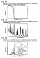
- the wavelength spectrum of the light generated by the intrinsic semiconductor because of the interband absorption is within a band of wavelengths that are shorter than the wavelength ⁇ g ( Fig. 1A ).
- the wavelength ⁇ g is referred as "cutoff wavelength”.
- resonant wavelength ⁇ r light of wavelengths around a wavelength that causes resonance in the optical structure
- thermo-optical converter Fig. 1C
- An example of the optical structure is a photonic crystal structure.
- a periodic refractive index distribution is formed, and light of a wavelength ⁇ r corresponding to the period forms standing waves.
- Such a photonic crystal structure that allows formation of standing waves of the resonant wavelength ⁇ r can be created by a person skilled in the art according to, for example, the disclosure of Patent literatures 1 and 2.
- another example of the optical structure includes one in which a plurality of members having a larger refractive index than that of a base is arranged on the base, which will be described later.
- each member standing waves formed by light of the wavelength ⁇ r determined by the size of the member are formed.
- the thermal emission source produces thermal emission having a resonant wavelength ⁇ r as the peak wavelength and having a wavelength spectrum having a narrower width than that of the spectrum of the thermal emission.
- the width of the bandgap of the intrinsic semiconductor changes depending on the temperature.
- the resonant wavelength in the thermo-optical converter is determined by the configuration of the optical structure and thus does not directly depend on the temperature.
- the refractive index changes according to the temperature, and along with the change in the refractive index, the light speed changes. Therefore, the resonant wavelength changes depending on the temperature.
- the cutoff wavelength ⁇ g and the resonant wavelength ⁇ r may be determined based on the width of the bandgap and the refractive index of the intrinsic semiconductor at the heating temperature when the thermal emission source according to the present invention is used.
- the present invention uses an intrinsic semiconductor and allows a wider range of material choices compared to a case where a quantum well structure obtained by combination of two types of semiconductors is used. Thus, a thermal emission source that produces light of an intended wavelength can easily be obtained.
- the intrinsic semiconductor any of various materials such as Si (silicon), SiC (silicon carbide) and Cu 2 O (copper oxide (I)) can be used.
- the cutoff wavelength ⁇ g is approximately 1700 nm (1400 K) in the case of Si, approximately 800 nm (2200 K) in the case of 3C-SiC (SiC having a cubic structure called "3C" from among SiCs), and is approximately 900 nm (1200 K) in the case of Cu 2 O.
- the cutoff wavelength ⁇ g described here is the value at the temperature indicated in each following bracket, and each of these temperatures is an example which may be used in the thermal emission source, which is determined in consideration of a melting point of each intrinsic semiconductor (Si: 1687K, 3C-SiC: 3100K or Cu 2 O: 1505K).
- the resonant wavelength ⁇ r be shorter than the cutoff wavelength ⁇ g to some extent.
- the resonant wavelength ⁇ r be 1600 nm (temperature: 1400 K) or shorter if the intrinsic semiconductor is Si, approximately 750 nm (2200 K) or shorter if the intrinsic semiconductor is 3C-SiC and approximately 850 nm (1200 K) or shorter if the intrinsic semiconductor is Cu 2 O.
- the optical structure be asymmetric with respect to the direction in which thermal emission is emitted from the thermal emission source. If the optical structure has no such asymmetry (that is, if the optical structure is symmetric in the direction), thermal emission is emitted both in the direction and in the direction opposite to the direction with the same intensity. If the optical structure has such asymmetry, thermal emission is emitted in one direction with a larger intensity.
- An example of the optical structure is a two-dimensional photonic crystal structure formed by periodically providing, in a plate member composed of an intrinsic semiconductor, areas each having a refractive index that is different from that of the plate member (different refractive index area). For each of the different refractive index areas, a hole (air or vacuum) can be used, or a member composed of a material that is different from the intrinsic semiconductor can be used. In this example, standing waves of a wavelength determined by the length of periodicity of the different refractive index areas are formed in the thermo-optical converter. Also, it is desirable that in the photonic crystal structure of this example, the different refractive index areas be asymmetric with respect to the direction perpendicular to the plate member.
- thermal emission can be emitted to one surface of the plate member with a larger intensity.
- the different refractive index areas having such asymmetry includes those having a triangular or trapezoidal shape in the cross-section perpendicular to the plate member; however, different refractive index areas that open in one surface of the plate member and do not open in the other surface of the plate member are desirable in terms of easy fabrication.
- the optical structure it is desirable to use such a structure that, on a surface of a base made of material having a refractive index lower than that of the intrinsic semiconductor, members (high-refractive index members) made of the intrinsic semiconductor and having the same shape are two-dimensionally arranged.
- the arrangement of the high-refractive index members does not need to be periodic.
- Such configuration allows formation of standing waves of a wavelength corresponding to the size of the high-refractive index members within each high-refractive index member. Therefore, the high-refractive index member itself can be made to function as an optical resonator (high-refractive index member optical resonator), enabling light whose wavelength of the standing waves is resonant wavelength to be selectively amplified. Since the optical structure is asymmetric as stated above, thermal emission can be emitted in one direction with a larger intensity.
- a three-dimensional photonic crystal structure having a three-dimensional periodic refractive index distribution may be used.
- a wavelength band in which light cannot exist within the structure can be formed irrespective of the direction of polarization of light.
- Such a wavelength band is formed for light for the reason similar to the bandgap for electrons, and is called "photonic bandgap" to distinguish from the bandgap for electrons.
- use of a three-dimensional photonic crystal structure enables selectively amplifying light of a predetermined wavelength that causes resonance in the three-dimensional photonic crystal structure (that is, light of a wavelength that can exist in the three-dimensional photonic crystal structure) while preventing production of light of wavelengths in the photonic bandgap, whereby light of the predetermined wavelength can efficiently be produced.
- the photovoltaic device includes a thermo-optical converter according to the present invention, and a solar cell for performing photoelectric conversion by receiving light produced by the thermo-optical converter and using the light having a wavelength band including the resonant wavelength.
- the solar cell receives light with the wavelength spectrum having a narrower width (but capable of making photoelectric conversion) than that of the wavelength spectrum of sunlight and including the resonant wavelength from the thermo-optical converter, the intensity of light having the wavelength band that makes photoelectric conversion is enhanced compared to a case where the solar cell directly receives sunlight.
- the photoelectric conversion efficiency is enhanced compared to a case where the solar cell directly receives sunlight.
- a silicon solar cell cannot perform photoelectric conversion at wavelengths about 1000 nm or longer, and thus it is desirable to set the resonant wavelength ⁇ r of the thermo-optical converter at 1000 nm or shorter.
- the present invention enables use of an intrinsic semiconductor that allows a wider range of material choices, enabling easy provision of a thermal emission source that produces narrow-band light having a desired peak wavelength.
- the present invention also enables provision of a photovoltaic device having a higher photoelectric conversion efficiency than that in a case where a solar cell directly receives sunlight.
- a thermal emission source 10 has an optical structure in which a plurality of columnar rods 11 made of an intrinsic semiconductor is arranged on a surface of a base 13 having a lower refractive index than that of the intrinsic semiconductor.
- Si refractive index: 3.4
- SiO 2 refractive index: 1.5
- a radius r of the rods 11 is 100 nm and a height h of the rods is 500 nm.
- the rods 11 are arranged at grid points of a square grid whose period length "a" is 600 nm; however, such periodic arrangement of the rods 11 is not essential to the present invention.
- a resonant wavelength ⁇ r in the optical structure in the present embodiment is determined by the refractive index n and the radius r of the rods 11 and the period length "a" of the square grid as described below.
- thermo-optical converter In the thermo-optical converter, light propagates in a height direction of the rods 11 along the rods 11 having a higher refractive index than that of the surrounding areas. Then, the light is reflected by an upper end and a lower end of each rod 11, whereby standing waves are generated and a resonant state of the light is formed.
- the resonant wavelength ⁇ r depends on the height h of the rods 11 and also depends on the radius r of the rods 11 since the effective refractive index varies when the light leaks from the rods 11.
- a difference in period length "a" of the rods 11 affects the resonant wavelength ⁇ r in terms of a difference in effective refractive index, but not so largely as a difference in radius r of the rods 11 does.
- the rods 11 having an excessively short period length "a” causes the wide range of electromagnetic field overlapped distribution among the rods 11 and interaction thereby occurs, resulting in variation in the resonant wavelength depending on the emission angle of the light.
- the period length "a” having a longer period length than that of a light emission wavelength invokes high-order diffraction, whereby radiation in one resonant mode is generated in a plurality of directions. Therefore, it is desirable that the period length "a” be longer than a distance of oozing of an electromagnetic field from each rod and be shorter than the light emission wavelength.
- the radius r of the rods 11 is set to 100 nm and the height h of the rods is set to 500 nm, whereby the wavelength ⁇ r of a resonant mode generated in each rod becomes 950 nm.
- the period length "a" is set to 600 nm, which is shorter than the resonant wavelength ⁇ r and sufficiently larger than the rod radius, whereby emission angle dependency is suppressed while the light emission intensity is maintained.
- thermo emission source 10 A principle of heat to light conversion by the thermal emission source 10 according to the first embodiment will be described.
- the thermal emission source 10 is heated to a temperature of around 1400 K, energy absorption caused by interband absorption in Si, which is an intrinsic semiconductor on the wavelength shorter than a cutoff wavelength ⁇ g for Si ⁇ 1700 nm (on the high energy side that is higher than 0.73 eV, which is photon energy corresponding to the cutoff wavelength ⁇ g ) occurs, and light emission corresponding to the energy occurs on the wavelength shorter than the cutoff wavelength ⁇ g (high energy side).
- a wavelength spectrum that can be obtained, by calculation, by the thermal emission source 10 according to the first embodiment is indicated in Fig. 4 .
- the calculation is performed for a case where the thermal emission source 10 is heated to 1400 K (1127°C).
- the wavelength spectrum has a single peak with a wavelength of approximately 950 nm as a peak top.
- the cutoff wavelength ⁇ g of Si is approximately 1700 nm (the corresponding photon energy is approximately 0.73 eV), and almost no light emission occurs on the wavelength longer than the cutoff wavelength ⁇ g .
- the spectrum of blackbody radiation becomes smaller as the wavelength is shorter, and the wavelength spectrum of the thermal emission source 10 becomes smaller accordingly as the wavelength is shorter.
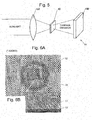
- a silicon solar cell cannot perform photoelectric conversion of light of wavelengths exceeding approximately 1000 nm. Therefore, as illustrated in Fig. 5 , a photovoltaic device 19 can be constructed by the thermal emission source 10, a collective lens 19A that collects sunlight to the thermal emission source 10, and a silicon solar cell 19B that receives thermal emission from the thermal emission source 10.
- photoelectric conversion can be performed in the silicon solar cell 19B after conversion of sunlight having a wide wavelength spectrum including light of wavelengths exceeding approximately 1000 nm to light having a peak of a wavelength spectrum at a wavelength of 1000 nm or shorter (950 nm in the present embodiment) by the thermal emission source 10, enabling enhancement in efficiency of the photoelectric conversion.
- Fig. 6A is an optical photomicrograph taken of the produced thermal emission source 10
- Fig. 6B is a magnified electron photomicrograph taken of the rods 11 and the base 13 of the thermal emission source 10.
- columnar rods 11 made of Si are arranged in a square grid in a square area 400 ⁇ m on a side on a surface of a plate base 13 made of SiO 2 and has a thickness of approximately 3 ⁇ m.
- a radius r of the rods 11 is 100 nm, a height h is 450 nm, and a periodic length "a" of the square grid is 500 nm.
- a plate heater 15 having a three-layer structure constructed of a layer of Ti, a layer of Pt and a layer of Ti in this order from the side close to the base 13 is provided, so as to be contact with a lower surface of the base 13 (surface on the opposite side of the surface on which the rods are provided).
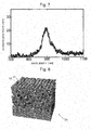
- the thermal emission source 10 was heated to a temperature of approximately 500 K, and the heat was converted to light according to the above-described principle, whereby light emission was obtained.
- a spectrum of the obtained light emission was measured, as shown in Fig. 7 , a wavelength spectrum having a peak at a wavelength of approximately 900 nm was obtained.
- the cutoff wavelength ⁇ g is 800 nm, which is shorter than that in the case of Si, and thus, the height and the radius of the rods 11 is set to be small compared to those in the case of Si.
- This obtains a thermal emission source that produces thermal emission having a wavelength spectrum with a peak on the wavelength shorter than 750 nm.
- a thermal emission source having such characteristics as above can suitably be used as a light source that emits thermal emission resulting from conversion of sunlight to a GaAs solar cell.
- the rods 11 are arranged in a square grid, arrangement in, e.g., a triangular grid may be employed.
- the shape of the rods 11 is a columnar shape, a shape such as a square rod, a cone or a pyramid may be employed.
- the surrounding areas of the rods 11 may be filled with a material having a lower refractive index than that of the rods 11, such as SiO 2 .
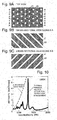
- a thermal emission source 20 has a structure in which columnar holes 22 each extending in a direction inclined by 45° from the normal to an upper surface of a block- member 21 composed of an intrinsic semiconductor are periodically formed.
- the columnar holes 22 are arranged in a triangular grid with a period length "a" in the upper surface of the block member 21.
- directions in which the columnar holes 42 in adjacent rows with grid points in the triangular grid extend are different by 90° from each other (alternation of the cross-sections along A-A and the cross-sections along B-B in Fig. 9A) (Fig. 9A and Fig. 9C ).
- Such configuration allows formation of a three-dimensional photonic crystal structure having a three-dimensional periodic refractive index distribution in a blockd member 21 composed of an intrinsic semiconductor (optical structure in the present embodiment).
- a material of the block member 21 is Si, and a period length "a" is 680 nm.
- a wavelength spectrum obtained by the thermal emission source 20 according to the second embodiment is indicated in Fig. 10 .
- a wavelength spectrum if the thermal emission source 20 is heated to 1300 K (1027°C) was obtained by calculation.
- a wavelength spectrum with a wavelength of approximately 1300 nm as a peak top was obtained.
- the material of the block member 21 is not limited to Si mentioned above and, e.g., SiC or Cu 2 O may be used. Also, instead of the columnar holes 22, members having a lower refractive index than that of the block member 21 may be used. Alternatively, as illustrated in Fig. 11 , a three-dimensional photonic crystal in which layers having rod members 29 each composed of an intrinsic semiconductor and arranged in parallel are stacked may be used, where a direction of the rod members in a layer is different by 90° from that of the rod members in a longitudinally adjacent layer (see Patent Literature 3).
- a thermal emission source 30 has a configuration in which holes (different-refractive index areas) 32 is periodically provided in a plate member 31, whereby a two-dimensional photonic crystal structure (optical structure in the present embodiment) is formed.
- a material of the plate member 31, in the present embodiment Si (refractive index: 3.4) is used.
- the holes 32 are arranged in a triangular grid.
- a planar shape of the individual holes 32 is a round shape.
- holes 32 each having a refractive index of approximately 1 are periodically arranged in the Si plate member 31 made of an intrinsic semiconductor and has the refractive index of 3.4, whereby a two-dimensional periodic refractive index distribution is formed.
- a period length "a" of the holes 32 is set to 600 nm. Also, a radius of the holes 32 is set to 150 nm. Also, the plate member 31 has a thickness of 500 nm, and the holes 32 are formed to have a depth of 200 nm from one surface of the plate member 31. The holes 32 are provided so as to form openings in one surface of the plate-like member 31 and not form the openings in the other surface, which forms asymmetry in a direction perpendicular to the plate member 31. Thus, thermal emission can be emitted with a larger intensity from the surface of the plate member 31 through which the holes 32 extend.
- an average refractive index in a case of combining the plate member 31 and the holes 32 is smaller, and thus, if the period length "a" remains constant, as the diameter is larger, the wavelengths in air is shorter.
- the thickness of the plate-like member 31 can be changed within a certain range while the resonant wavelength is maintained to be similar, by adjusting, e.g., the diameter, depth or periodicity of the holes.
- excessive increase in the thickness causes energy absorption by intrinsic carriers in the intrinsic semiconductor, which may result in undesired light emission on the wavelength longer than the cutoff wavelength ⁇ g .
- each energy absorptance of a Si plate member having a thickness of 0.5 ⁇ m (500 nm), which is the same as that of the present embodiment, and Si plate members having a thickness of 10 ⁇ m and 100 ⁇ m, respectively, when the members are heated to 1400 K (1127°C) was obtained by calculation. As shown in Fig.
- the absorptance has a value of almost 0.7 where the thickness of the plate member is 100 ⁇ m, and the absorptance has a value of 0.30 to 0.35 where the thickness is 10 ⁇ m, whereas the absorptance has a value of almost zero where the thickness is 0.5 ⁇ m.
- the thickness of the plate member 31 be thin.
- the thickness of the plate member 31 is extremely small, light emission having the resonant wavelength also decreases, and thus, it is desirable to select a proper thickness in view of this point. In the present embodiment, 0.5 ⁇ m is optimum.
- Such unnecessary light emission on the long wavelength side may occur in the first and second embodiments.
- an effective thickness of intrinsic semiconductor averaged in a direction parallel to a surface of the base 13 can be changed by changing the height or diameter of the rods 11 made of the intrinsic semiconductor, enabling adjustment so that light emission on the long wavelength side is suppressed.
- the periodicity of the columnar holes 22 or the rod members 29 is adjusted so that a three-dimensional photonic bandgap is formed on the wavelength longer than the resonant wavelength, whereby light on the longer wavelength cannot exist in the three-dimensional photonic crystal structure. Therefore, production of the light is thus suppressed.
- Si is used for the material of the plate member 31
- an intrinsic semiconductor other than Si such as SiC or Cu 2 O
- the holes 32 are arranged in a triangular grid has been described up to here, arrangement in, e.g., a square gird may be employed.
- a planar shape of the holes 32 is a round shape, a planar shape other than a round shape such as a regular triangle shape may be employed.
- members having a lower refractive index than that of the material of the plate member 31 such as members made of SiO 2 may be provided.
Landscapes
- Physics & Mathematics (AREA)
- General Physics & Mathematics (AREA)
- Spectroscopy & Molecular Physics (AREA)
- Chemical & Material Sciences (AREA)
- Crystallography & Structural Chemistry (AREA)
- Optics & Photonics (AREA)
- Photovoltaic Devices (AREA)
- Optical Filters (AREA)
- Led Device Packages (AREA)
Applications Claiming Priority (2)
| Application Number | Priority Date | Filing Date | Title |
|---|---|---|---|
| JP2013047281 | 2013-03-08 | ||
| PCT/JP2014/055056 WO2014136671A1 (fr) | 2013-03-08 | 2014-02-28 | Source de lumière à rayonnement thermique |
Publications (3)
| Publication Number | Publication Date |
|---|---|
| EP2966773A1 true EP2966773A1 (fr) | 2016-01-13 |
| EP2966773A4 EP2966773A4 (fr) | 2016-04-13 |
| EP2966773B1 EP2966773B1 (fr) | 2019-06-12 |
Family
ID=51491190
Family Applications (1)
| Application Number | Title | Priority Date | Filing Date |
|---|---|---|---|
| EP14761195.8A Active EP2966773B1 (fr) | 2013-03-08 | 2014-02-28 | Source de lumière à rayonnement thermique |
Country Status (5)
| Country | Link |
|---|---|
| US (2) | US20160049897A1 (fr) |
| EP (1) | EP2966773B1 (fr) |
| JP (1) | JP6227627B2 (fr) |
| CN (1) | CN105027428B (fr) |
| WO (1) | WO2014136671A1 (fr) |
Cited By (1)
| Publication number | Priority date | Publication date | Assignee | Title |
|---|---|---|---|---|
| EP3291283A1 (fr) * | 2016-09-05 | 2018-03-07 | Commissariat à l'Energie Atomique et aux Energies Alternatives | Surface d'emission de rayonnement infrarouge ir a emissivite thermique elevee et a grande duree de vie et son procede de fabrication |
Families Citing this family (7)
| Publication number | Priority date | Publication date | Assignee | Title |
|---|---|---|---|---|
| JP6597997B2 (ja) * | 2015-03-31 | 2019-10-30 | 大阪瓦斯株式会社 | 熱光発電機 |
| WO2017141682A1 (fr) * | 2016-02-16 | 2017-08-24 | ローム株式会社 | Élément de conversion thermo-optique et module de conversion thermoélectrique |
| JP6671654B2 (ja) * | 2016-03-01 | 2020-03-25 | 大阪瓦斯株式会社 | 熱輻射光源 |
| CN105957915B (zh) * | 2016-05-16 | 2018-07-06 | 华南师范大学 | 一种耐高温的太阳能光谱选择性吸收与辐射结构 |
| CN106050586B (zh) | 2016-08-08 | 2018-08-07 | 浙江大学 | 基于特征吸收光谱的气体体吸热太阳能发电方法及装置 |
| JP6762533B2 (ja) * | 2016-09-09 | 2020-09-30 | 大阪瓦斯株式会社 | 熱輻射光源および光源装置 |
| US10819270B2 (en) | 2018-03-16 | 2020-10-27 | Uchicago Argonne, Llc | High temperature selective emitters via critical coupling of weak absorbers |
Family Cites Families (16)
| Publication number | Priority date | Publication date | Assignee | Title |
|---|---|---|---|---|
| JP2001074955A (ja) | 1999-08-31 | 2001-03-23 | Susumu Noda | フォトニック結晶導波路 |
| US6611085B1 (en) * | 2001-08-27 | 2003-08-26 | Sandia Corporation | Photonically engineered incandescent emitter |
| WO2003073055A1 (fr) * | 2002-02-28 | 2003-09-04 | Shin-Etsu Handotai Co., Ltd. | Systeme de mesure de la temperature, dispositif de chauffage utilisant le systeme, procede de production d'une plaquette a semi-conducteurs, element translucide de protection contre les rayons calorifiques, element reflechissant la lumiere visible, miroir reflechissant utilisant un systeme d'exposition, dispositif a semi-co |
| JP2003342097A (ja) * | 2002-05-28 | 2003-12-03 | Japan Aviation Electronics Industry Ltd | フォトニック結晶の作製方法 |
| US6859304B2 (en) * | 2002-08-09 | 2005-02-22 | Energy Conversion Devices, Inc. | Photonic crystals and devices having tunability and switchability |
| KR101128944B1 (ko) | 2004-03-05 | 2012-03-27 | 로무 가부시키가이샤 | 2차원 포토닉 결정 면발광 레이저광원 |
| WO2007029661A1 (fr) | 2005-09-05 | 2007-03-15 | Kyoto University | Source de lumière laser émettant de la lumière à la surface d’un cristal photonique bidimensionnel |
| US7630589B2 (en) * | 2007-01-09 | 2009-12-08 | The Board Of Trustees Of The Leland Stanford Junior University | Photonic crystal structure sensor |
| JP5272173B2 (ja) * | 2007-03-26 | 2013-08-28 | 国立大学法人京都大学 | 2次元フォトニック結晶 |
| US8556389B2 (en) * | 2011-02-04 | 2013-10-15 | Kateeva, Inc. | Low-profile MEMS thermal printhead die having backside electrical connections |
| US7825366B2 (en) * | 2007-09-13 | 2010-11-02 | Raytheon Company | Methods and systems for extracting energy from a heat source using photonic crystals with defect cavities |
| CN102792456B (zh) * | 2010-01-07 | 2015-09-09 | 夏普株式会社 | 太阳能电池、太阳能电池板和具备太阳能电池的装置 |
| SG10201501429WA (en) * | 2010-02-28 | 2015-04-29 | Mtpv Power Corp | Micron-gap thermal photovoltaic large scale sub-micron gap method and apparatus |
| US9116537B2 (en) * | 2010-05-21 | 2015-08-25 | Massachusetts Institute Of Technology | Thermophotovoltaic energy generation |
| JP5830468B2 (ja) * | 2010-10-29 | 2015-12-09 | スタンレー電気株式会社 | 発電装置 |
| TWI458122B (zh) * | 2011-11-23 | 2014-10-21 | 東芝股份有限公司 | 半導體發光元件 |
-
2014
- 2014-02-28 US US14/773,663 patent/US20160049897A1/en not_active Abandoned
- 2014-02-28 WO PCT/JP2014/055056 patent/WO2014136671A1/fr not_active Ceased
- 2014-02-28 CN CN201480013123.7A patent/CN105027428B/zh not_active Expired - Fee Related
- 2014-02-28 EP EP14761195.8A patent/EP2966773B1/fr active Active
- 2014-02-28 JP JP2015504273A patent/JP6227627B2/ja active Active
-
2020
- 2020-08-20 US US16/998,182 patent/US20200382048A1/en not_active Abandoned
Cited By (4)
| Publication number | Priority date | Publication date | Assignee | Title |
|---|---|---|---|---|
| EP3291283A1 (fr) * | 2016-09-05 | 2018-03-07 | Commissariat à l'Energie Atomique et aux Energies Alternatives | Surface d'emission de rayonnement infrarouge ir a emissivite thermique elevee et a grande duree de vie et son procede de fabrication |
| US20180066993A1 (en) * | 2016-09-05 | 2018-03-08 | Commissariat A L'energie Atomique Et Aux Energies Alternatives | Infrared radiation emission surface having a high thermal emissivity and a long life time and its manufacturing method |
| FR3055738A1 (fr) * | 2016-09-05 | 2018-03-09 | Commissariat A L'energie Atomique Et Aux Energies Alternatives | Surface d'emission de rayonnement infrarouge ir a emissivite thermique elevee et a grande duree de vie et son procede de fabrication |
| US10054489B2 (en) | 2016-09-05 | 2018-08-21 | Commissariat A L'energie Atomique Aux Energies Alternatives | Infrared radiation emission surface having a high thermal emissivity and a long life time and its manufacturing method |
Also Published As
| Publication number | Publication date |
|---|---|
| US20200382048A1 (en) | 2020-12-03 |
| WO2014136671A1 (fr) | 2014-09-12 |
| US20160049897A1 (en) | 2016-02-18 |
| EP2966773A4 (fr) | 2016-04-13 |
| JP6227627B2 (ja) | 2017-11-08 |
| CN105027428A (zh) | 2015-11-04 |
| EP2966773B1 (fr) | 2019-06-12 |
| CN105027428B (zh) | 2017-09-22 |
| JPWO2014136671A1 (ja) | 2017-02-09 |
Similar Documents
| Publication | Publication Date | Title |
|---|---|---|
| US20200382048A1 (en) | Thermal radiation light source | |
| Haverkort et al. | Fundamentals of the nanowire solar cell: Optimization of the open circuit voltage | |
| Capellini et al. | Strain analysis in SiN/Ge microstructures obtained via Si-complementary metal oxide semiconductor compatible approach | |
| JP6169614B2 (ja) | プラズモン電極を有する光伝導装置 | |
| Demésy et al. | Solar energy trapping with modulated silicon nanowire photonic crystals | |
| CN107490437B (zh) | 红外线传感器 | |
| Weih et al. | Interband cascade lasers with room temperature threshold current densities below 100 A/cm2 | |
| US9065253B2 (en) | Strain modulated nanostructures for optoelectronic devices and associated systems and methods | |
| KR102322321B1 (ko) | 레이디얼 p-n 접합 나노와이어 태양전지 | |
| US20150053261A1 (en) | Solar cell | |
| CN111886704B (zh) | 光检测器 | |
| CN112204757B (zh) | 基于本征等离子体激元-激子极化子的光电器件 | |
| JP5607589B2 (ja) | 量子ドット配列材料並びにこれを用いた光電変換素子及び波長変換素子 | |
| JPWO2017141682A1 (ja) | 熱光変換素子および熱電変換素子 | |
| US7659536B2 (en) | High performance hyperspectral detectors using photon controlling cavities | |
| JP2014216549A (ja) | フォトニック結晶光検出器 | |
| Shigeta et al. | Enhancement of photocurrent in ultrathin active-layer photodetecting devices with photonic crystals | |
| JP6846035B2 (ja) | 熱輻射光発電装置 | |
| Liang et al. | High-Power 2.2-$\mu $ m Diode Lasers With Heavily Strained Active Region | |
| CN101494243A (zh) | 光子晶体耦合窄带响应量子阱红外探测器 | |
| JP2008053134A (ja) | 2次元フォトニック結晶熱輻射光源 | |
| Hussein et al. | Effective modelling of silicon nanowire solar cells | |
| Liu et al. | Two-dimensional heterojunction photovoltaic cells with low spontaneous-radiation loss and high efficiency limit | |
| Mahmoud et al. | Optical and electrical characteristics of highly efficient flower-shaped silicon nanowires solar cell | |
| Koerperick et al. | InAs∕ GaSb cascaded active region superlattice light emitting diodes for operation at 3.8 μm |
Legal Events
| Date | Code | Title | Description |
|---|---|---|---|
| PUAI | Public reference made under article 153(3) epc to a published international application that has entered the european phase |
Free format text: ORIGINAL CODE: 0009012 |
|
| 17P | Request for examination filed |
Effective date: 20151006 |
|
| AK | Designated contracting states |
Kind code of ref document: A1 Designated state(s): AL AT BE BG CH CY CZ DE DK EE ES FI FR GB GR HR HU IE IS IT LI LT LU LV MC MK MT NL NO PL PT RO RS SE SI SK SM TR |
|
| AX | Request for extension of the european patent |
Extension state: BA ME |
|
| A4 | Supplementary search report drawn up and despatched |
Effective date: 20160310 |
|
| RIC1 | Information provided on ipc code assigned before grant |
Ipc: H02S 10/30 20140101AFI20160304BHEP Ipc: H01L 31/054 20140101ALI20160304BHEP Ipc: H01K 1/04 20060101ALI20160304BHEP |
|
| DAX | Request for extension of the european patent (deleted) | ||
| GRAP | Despatch of communication of intention to grant a patent |
Free format text: ORIGINAL CODE: EPIDOSNIGR1 |
|
| STAA | Information on the status of an ep patent application or granted ep patent |
Free format text: STATUS: GRANT OF PATENT IS INTENDED |
|
| INTG | Intention to grant announced |
Effective date: 20181220 |
|
| GRAS | Grant fee paid |
Free format text: ORIGINAL CODE: EPIDOSNIGR3 |
|
| GRAA | (expected) grant |
Free format text: ORIGINAL CODE: 0009210 |
|
| STAA | Information on the status of an ep patent application or granted ep patent |
Free format text: STATUS: THE PATENT HAS BEEN GRANTED |
|
| AK | Designated contracting states |
Kind code of ref document: B1 Designated state(s): AL AT BE BG CH CY CZ DE DK EE ES FI FR GB GR HR HU IE IS IT LI LT LU LV MC MK MT NL NO PL PT RO RS SE SI SK SM TR |
|
| REG | Reference to a national code |
Ref country code: GB Ref legal event code: FG4D |
|
| REG | Reference to a national code |
Ref country code: CH Ref legal event code: EP |
|
| REG | Reference to a national code |
Ref country code: AT Ref legal event code: REF Ref document number: 1143905 Country of ref document: AT Kind code of ref document: T Effective date: 20190615 |
|
| REG | Reference to a national code |
Ref country code: DE Ref legal event code: R096 Ref document number: 602014048233 Country of ref document: DE |
|
| REG | Reference to a national code |
Ref country code: IE Ref legal event code: FG4D |
|
| REG | Reference to a national code |
Ref country code: NL Ref legal event code: MP Effective date: 20190612 |
|
| REG | Reference to a national code |
Ref country code: LT Ref legal event code: MG4D |
|
| PG25 | Lapsed in a contracting state [announced via postgrant information from national office to epo] |
Ref country code: AL Free format text: LAPSE BECAUSE OF FAILURE TO SUBMIT A TRANSLATION OF THE DESCRIPTION OR TO PAY THE FEE WITHIN THE PRESCRIBED TIME-LIMIT Effective date: 20190612 Ref country code: LT Free format text: LAPSE BECAUSE OF FAILURE TO SUBMIT A TRANSLATION OF THE DESCRIPTION OR TO PAY THE FEE WITHIN THE PRESCRIBED TIME-LIMIT Effective date: 20190612 Ref country code: FI Free format text: LAPSE BECAUSE OF FAILURE TO SUBMIT A TRANSLATION OF THE DESCRIPTION OR TO PAY THE FEE WITHIN THE PRESCRIBED TIME-LIMIT Effective date: 20190612 Ref country code: NO Free format text: LAPSE BECAUSE OF FAILURE TO SUBMIT A TRANSLATION OF THE DESCRIPTION OR TO PAY THE FEE WITHIN THE PRESCRIBED TIME-LIMIT Effective date: 20190912 Ref country code: SE Free format text: LAPSE BECAUSE OF FAILURE TO SUBMIT A TRANSLATION OF THE DESCRIPTION OR TO PAY THE FEE WITHIN THE PRESCRIBED TIME-LIMIT Effective date: 20190612 Ref country code: HR Free format text: LAPSE BECAUSE OF FAILURE TO SUBMIT A TRANSLATION OF THE DESCRIPTION OR TO PAY THE FEE WITHIN THE PRESCRIBED TIME-LIMIT Effective date: 20190612 |
|
| PG25 | Lapsed in a contracting state [announced via postgrant information from national office to epo] |
Ref country code: LV Free format text: LAPSE BECAUSE OF FAILURE TO SUBMIT A TRANSLATION OF THE DESCRIPTION OR TO PAY THE FEE WITHIN THE PRESCRIBED TIME-LIMIT Effective date: 20190612 Ref country code: RS Free format text: LAPSE BECAUSE OF FAILURE TO SUBMIT A TRANSLATION OF THE DESCRIPTION OR TO PAY THE FEE WITHIN THE PRESCRIBED TIME-LIMIT Effective date: 20190612 Ref country code: BG Free format text: LAPSE BECAUSE OF FAILURE TO SUBMIT A TRANSLATION OF THE DESCRIPTION OR TO PAY THE FEE WITHIN THE PRESCRIBED TIME-LIMIT Effective date: 20190912 Ref country code: GR Free format text: LAPSE BECAUSE OF FAILURE TO SUBMIT A TRANSLATION OF THE DESCRIPTION OR TO PAY THE FEE WITHIN THE PRESCRIBED TIME-LIMIT Effective date: 20190913 |
|
| REG | Reference to a national code |
Ref country code: AT Ref legal event code: MK05 Ref document number: 1143905 Country of ref document: AT Kind code of ref document: T Effective date: 20190612 |
|
| PG25 | Lapsed in a contracting state [announced via postgrant information from national office to epo] |
Ref country code: PT Free format text: LAPSE BECAUSE OF FAILURE TO SUBMIT A TRANSLATION OF THE DESCRIPTION OR TO PAY THE FEE WITHIN THE PRESCRIBED TIME-LIMIT Effective date: 20191014 Ref country code: CZ Free format text: LAPSE BECAUSE OF FAILURE TO SUBMIT A TRANSLATION OF THE DESCRIPTION OR TO PAY THE FEE WITHIN THE PRESCRIBED TIME-LIMIT Effective date: 20190612 Ref country code: NL Free format text: LAPSE BECAUSE OF FAILURE TO SUBMIT A TRANSLATION OF THE DESCRIPTION OR TO PAY THE FEE WITHIN THE PRESCRIBED TIME-LIMIT Effective date: 20190612 Ref country code: AT Free format text: LAPSE BECAUSE OF FAILURE TO SUBMIT A TRANSLATION OF THE DESCRIPTION OR TO PAY THE FEE WITHIN THE PRESCRIBED TIME-LIMIT Effective date: 20190612 Ref country code: RO Free format text: LAPSE BECAUSE OF FAILURE TO SUBMIT A TRANSLATION OF THE DESCRIPTION OR TO PAY THE FEE WITHIN THE PRESCRIBED TIME-LIMIT Effective date: 20190612 Ref country code: EE Free format text: LAPSE BECAUSE OF FAILURE TO SUBMIT A TRANSLATION OF THE DESCRIPTION OR TO PAY THE FEE WITHIN THE PRESCRIBED TIME-LIMIT Effective date: 20190612 Ref country code: SK Free format text: LAPSE BECAUSE OF FAILURE TO SUBMIT A TRANSLATION OF THE DESCRIPTION OR TO PAY THE FEE WITHIN THE PRESCRIBED TIME-LIMIT Effective date: 20190612 |
|
| PG25 | Lapsed in a contracting state [announced via postgrant information from national office to epo] |
Ref country code: ES Free format text: LAPSE BECAUSE OF FAILURE TO SUBMIT A TRANSLATION OF THE DESCRIPTION OR TO PAY THE FEE WITHIN THE PRESCRIBED TIME-LIMIT Effective date: 20190612 Ref country code: IT Free format text: LAPSE BECAUSE OF FAILURE TO SUBMIT A TRANSLATION OF THE DESCRIPTION OR TO PAY THE FEE WITHIN THE PRESCRIBED TIME-LIMIT Effective date: 20190612 Ref country code: SM Free format text: LAPSE BECAUSE OF FAILURE TO SUBMIT A TRANSLATION OF THE DESCRIPTION OR TO PAY THE FEE WITHIN THE PRESCRIBED TIME-LIMIT Effective date: 20190612 Ref country code: IS Free format text: LAPSE BECAUSE OF FAILURE TO SUBMIT A TRANSLATION OF THE DESCRIPTION OR TO PAY THE FEE WITHIN THE PRESCRIBED TIME-LIMIT Effective date: 20191012 |
|
| REG | Reference to a national code |
Ref country code: DE Ref legal event code: R097 Ref document number: 602014048233 Country of ref document: DE |
|
| PG25 | Lapsed in a contracting state [announced via postgrant information from national office to epo] |
Ref country code: TR Free format text: LAPSE BECAUSE OF FAILURE TO SUBMIT A TRANSLATION OF THE DESCRIPTION OR TO PAY THE FEE WITHIN THE PRESCRIBED TIME-LIMIT Effective date: 20190612 |
|
| PLBE | No opposition filed within time limit |
Free format text: ORIGINAL CODE: 0009261 |
|
| STAA | Information on the status of an ep patent application or granted ep patent |
Free format text: STATUS: NO OPPOSITION FILED WITHIN TIME LIMIT |
|
| PG25 | Lapsed in a contracting state [announced via postgrant information from national office to epo] |
Ref country code: DK Free format text: LAPSE BECAUSE OF FAILURE TO SUBMIT A TRANSLATION OF THE DESCRIPTION OR TO PAY THE FEE WITHIN THE PRESCRIBED TIME-LIMIT Effective date: 20190612 Ref country code: PL Free format text: LAPSE BECAUSE OF FAILURE TO SUBMIT A TRANSLATION OF THE DESCRIPTION OR TO PAY THE FEE WITHIN THE PRESCRIBED TIME-LIMIT Effective date: 20190612 |
|
| 26N | No opposition filed |
Effective date: 20200313 |
|
| PG25 | Lapsed in a contracting state [announced via postgrant information from national office to epo] |
Ref country code: IS Free format text: LAPSE BECAUSE OF FAILURE TO SUBMIT A TRANSLATION OF THE DESCRIPTION OR TO PAY THE FEE WITHIN THE PRESCRIBED TIME-LIMIT Effective date: 20200224 Ref country code: SI Free format text: LAPSE BECAUSE OF FAILURE TO SUBMIT A TRANSLATION OF THE DESCRIPTION OR TO PAY THE FEE WITHIN THE PRESCRIBED TIME-LIMIT Effective date: 20190612 |
|
| PG2D | Information on lapse in contracting state deleted |
Ref country code: IS |
|
| REG | Reference to a national code |
Ref country code: CH Ref legal event code: PL |
|
| GBPC | Gb: european patent ceased through non-payment of renewal fee |
Effective date: 20200228 |
|
| REG | Reference to a national code |
Ref country code: BE Ref legal event code: MM Effective date: 20200229 |
|
| PG25 | Lapsed in a contracting state [announced via postgrant information from national office to epo] |
Ref country code: LU Free format text: LAPSE BECAUSE OF NON-PAYMENT OF DUE FEES Effective date: 20200228 Ref country code: MC Free format text: LAPSE BECAUSE OF FAILURE TO SUBMIT A TRANSLATION OF THE DESCRIPTION OR TO PAY THE FEE WITHIN THE PRESCRIBED TIME-LIMIT Effective date: 20190612 |
|
| PG25 | Lapsed in a contracting state [announced via postgrant information from national office to epo] |
Ref country code: CH Free format text: LAPSE BECAUSE OF NON-PAYMENT OF DUE FEES Effective date: 20200229 Ref country code: LI Free format text: LAPSE BECAUSE OF NON-PAYMENT OF DUE FEES Effective date: 20200229 |
|
| PG25 | Lapsed in a contracting state [announced via postgrant information from national office to epo] |
Ref country code: FR Free format text: LAPSE BECAUSE OF NON-PAYMENT OF DUE FEES Effective date: 20200229 Ref country code: GB Free format text: LAPSE BECAUSE OF NON-PAYMENT OF DUE FEES Effective date: 20200228 Ref country code: IE Free format text: LAPSE BECAUSE OF NON-PAYMENT OF DUE FEES Effective date: 20200228 |
|
| PG25 | Lapsed in a contracting state [announced via postgrant information from national office to epo] |
Ref country code: BE Free format text: LAPSE BECAUSE OF NON-PAYMENT OF DUE FEES Effective date: 20200229 |
|
| PG25 | Lapsed in a contracting state [announced via postgrant information from national office to epo] |
Ref country code: MT Free format text: LAPSE BECAUSE OF FAILURE TO SUBMIT A TRANSLATION OF THE DESCRIPTION OR TO PAY THE FEE WITHIN THE PRESCRIBED TIME-LIMIT Effective date: 20190612 Ref country code: CY Free format text: LAPSE BECAUSE OF FAILURE TO SUBMIT A TRANSLATION OF THE DESCRIPTION OR TO PAY THE FEE WITHIN THE PRESCRIBED TIME-LIMIT Effective date: 20190612 |
|
| PG25 | Lapsed in a contracting state [announced via postgrant information from national office to epo] |
Ref country code: MK Free format text: LAPSE BECAUSE OF FAILURE TO SUBMIT A TRANSLATION OF THE DESCRIPTION OR TO PAY THE FEE WITHIN THE PRESCRIBED TIME-LIMIT Effective date: 20190612 |
|
| REG | Reference to a national code |
Ref country code: DE Ref legal event code: R081 Ref document number: 602014048233 Country of ref document: DE Owner name: KYOTO UNIVERSITY, KYOTO-SHI, JP Free format text: FORMER OWNER: JAPAN SCIENCE AND TECHNOLOGY AGENCY, KAWAGUCHI-SHI, SAITAMA, JP |
|
| PGFP | Annual fee paid to national office [announced via postgrant information from national office to epo] |
Ref country code: DE Payment date: 20230621 Year of fee payment: 10 |
|
| REG | Reference to a national code |
Ref country code: DE Ref legal event code: R119 Ref document number: 602014048233 Country of ref document: DE |
|
| PG25 | Lapsed in a contracting state [announced via postgrant information from national office to epo] |
Ref country code: DE Free format text: LAPSE BECAUSE OF NON-PAYMENT OF DUE FEES Effective date: 20240903 |
|
| PG25 | Lapsed in a contracting state [announced via postgrant information from national office to epo] |
Ref country code: DE Free format text: LAPSE BECAUSE OF NON-PAYMENT OF DUE FEES Effective date: 20240903 |