EP2966945A1 - Procédé de fabrication de dispositifs électroniques en couches - Google Patents
Procédé de fabrication de dispositifs électroniques en couches Download PDFInfo
- Publication number
- EP2966945A1 EP2966945A1 EP15173294.8A EP15173294A EP2966945A1 EP 2966945 A1 EP2966945 A1 EP 2966945A1 EP 15173294 A EP15173294 A EP 15173294A EP 2966945 A1 EP2966945 A1 EP 2966945A1
- Authority
- EP
- European Patent Office
- Prior art keywords
- layer
- printing
- electrical
- electrical device
- stacking
- Prior art date
- Legal status (The legal status is an assumption and is not a legal conclusion. Google has not performed a legal analysis and makes no representation as to the accuracy of the status listed.)
- Granted
Links
Images
Classifications
-
- H—ELECTRICITY
- H05—ELECTRIC TECHNIQUES NOT OTHERWISE PROVIDED FOR
- H05K—PRINTED CIRCUITS; CASINGS OR CONSTRUCTIONAL DETAILS OF ELECTRIC APPARATUS; MANUFACTURE OF ASSEMBLAGES OF ELECTRICAL COMPONENTS
- H05K1/00—Printed circuits
- H05K1/16—Printed circuits incorporating printed electric components, e.g. printed resistors, capacitors or inductors
-
- H—ELECTRICITY
- H05—ELECTRIC TECHNIQUES NOT OTHERWISE PROVIDED FOR
- H05K—PRINTED CIRCUITS; CASINGS OR CONSTRUCTIONAL DETAILS OF ELECTRIC APPARATUS; MANUFACTURE OF ASSEMBLAGES OF ELECTRICAL COMPONENTS
- H05K1/00—Printed circuits
- H05K1/02—Details
- H05K1/09—Use of materials for the conductive, e.g. metallic pattern
- H05K1/092—Dispersed materials, e.g. conductive pastes or inks
-
- B—PERFORMING OPERATIONS; TRANSPORTING
- B32—LAYERED PRODUCTS
- B32B—LAYERED PRODUCTS, i.e. PRODUCTS BUILT-UP OF STRATA OF FLAT OR NON-FLAT, e.g. CELLULAR OR HONEYCOMB, FORM
- B32B37/00—Methods or apparatus for laminating, e.g. by curing or by ultrasonic bonding
- B32B37/06—Methods or apparatus for laminating, e.g. by curing or by ultrasonic bonding characterised by the heating method
-
- C—CHEMISTRY; METALLURGY
- C23—COATING METALLIC MATERIAL; COATING MATERIAL WITH METALLIC MATERIAL; CHEMICAL SURFACE TREATMENT; DIFFUSION TREATMENT OF METALLIC MATERIAL; COATING BY VACUUM EVAPORATION, BY SPUTTERING, BY ION IMPLANTATION OR BY CHEMICAL VAPOUR DEPOSITION, IN GENERAL; INHIBITING CORROSION OF METALLIC MATERIAL OR INCRUSTATION IN GENERAL
- C23C—COATING METALLIC MATERIAL; COATING MATERIAL WITH METALLIC MATERIAL; SURFACE TREATMENT OF METALLIC MATERIAL BY DIFFUSION INTO THE SURFACE, BY CHEMICAL CONVERSION OR SUBSTITUTION; COATING BY VACUUM EVAPORATION, BY SPUTTERING, BY ION IMPLANTATION OR BY CHEMICAL VAPOUR DEPOSITION, IN GENERAL
- C23C18/00—Chemical coating by decomposition of either liquid compounds or solutions of the coating forming compounds, without leaving reaction products of surface material in the coating; Contact plating
- C23C18/16—Chemical coating by decomposition of either liquid compounds or solutions of the coating forming compounds, without leaving reaction products of surface material in the coating; Contact plating by reduction or substitution, e.g. electroless plating
- C23C18/1601—Process or apparatus
- C23C18/1633—Process of electroless plating
-
- H—ELECTRICITY
- H05—ELECTRIC TECHNIQUES NOT OTHERWISE PROVIDED FOR
- H05K—PRINTED CIRCUITS; CASINGS OR CONSTRUCTIONAL DETAILS OF ELECTRIC APPARATUS; MANUFACTURE OF ASSEMBLAGES OF ELECTRICAL COMPONENTS
- H05K1/00—Printed circuits
- H05K1/02—Details
- H05K1/0296—Conductive pattern lay-out details not covered by sub groups H05K1/02 - H05K1/0295
- H05K1/0298—Multilayer circuits
-
- H—ELECTRICITY
- H05—ELECTRIC TECHNIQUES NOT OTHERWISE PROVIDED FOR
- H05K—PRINTED CIRCUITS; CASINGS OR CONSTRUCTIONAL DETAILS OF ELECTRIC APPARATUS; MANUFACTURE OF ASSEMBLAGES OF ELECTRICAL COMPONENTS
- H05K1/00—Printed circuits
- H05K1/16—Printed circuits incorporating printed electric components, e.g. printed resistors, capacitors or inductors
- H05K1/165—Printed circuits incorporating printed electric components, e.g. printed resistors, capacitors or inductors incorporating printed inductors
-
- H—ELECTRICITY
- H05—ELECTRIC TECHNIQUES NOT OTHERWISE PROVIDED FOR
- H05K—PRINTED CIRCUITS; CASINGS OR CONSTRUCTIONAL DETAILS OF ELECTRIC APPARATUS; MANUFACTURE OF ASSEMBLAGES OF ELECTRICAL COMPONENTS
- H05K3/00—Apparatus or processes for manufacturing printed circuits
- H05K3/10—Apparatus or processes for manufacturing printed circuits in which conductive material is applied to the insulating support in such a manner as to form the desired conductive pattern
- H05K3/12—Apparatus or processes for manufacturing printed circuits in which conductive material is applied to the insulating support in such a manner as to form the desired conductive pattern using thick film techniques, e.g. printing techniques to apply the conductive material or similar techniques for applying conductive paste or ink patterns
-
- H—ELECTRICITY
- H05—ELECTRIC TECHNIQUES NOT OTHERWISE PROVIDED FOR
- H05K—PRINTED CIRCUITS; CASINGS OR CONSTRUCTIONAL DETAILS OF ELECTRIC APPARATUS; MANUFACTURE OF ASSEMBLAGES OF ELECTRICAL COMPONENTS
- H05K3/00—Apparatus or processes for manufacturing printed circuits
- H05K3/36—Assembling printed circuits with other printed circuits
-
- H—ELECTRICITY
- H05—ELECTRIC TECHNIQUES NOT OTHERWISE PROVIDED FOR
- H05K—PRINTED CIRCUITS; CASINGS OR CONSTRUCTIONAL DETAILS OF ELECTRIC APPARATUS; MANUFACTURE OF ASSEMBLAGES OF ELECTRICAL COMPONENTS
- H05K3/00—Apparatus or processes for manufacturing printed circuits
- H05K3/46—Manufacturing multilayer circuits
- H05K3/4611—Manufacturing multilayer circuits by laminating two or more circuit boards
- H05K3/4614—Manufacturing multilayer circuits by laminating two or more circuit boards the electrical connections between the circuit boards being made during lamination
- H05K3/4617—Manufacturing multilayer circuits by laminating two or more circuit boards the electrical connections between the circuit boards being made during lamination characterized by laminating only or mainly similar single-sided circuit boards
-
- B—PERFORMING OPERATIONS; TRANSPORTING
- B32—LAYERED PRODUCTS
- B32B—LAYERED PRODUCTS, i.e. PRODUCTS BUILT-UP OF STRATA OF FLAT OR NON-FLAT, e.g. CELLULAR OR HONEYCOMB, FORM
- B32B2305/00—Condition, form or state of the layers or laminate
- B32B2305/72—Cured, e.g. vulcanised, cross-linked
-
- H—ELECTRICITY
- H05—ELECTRIC TECHNIQUES NOT OTHERWISE PROVIDED FOR
- H05K—PRINTED CIRCUITS; CASINGS OR CONSTRUCTIONAL DETAILS OF ELECTRIC APPARATUS; MANUFACTURE OF ASSEMBLAGES OF ELECTRICAL COMPONENTS
- H05K2201/00—Indexing scheme relating to printed circuits covered by H05K1/00
- H05K2201/01—Dielectrics
- H05K2201/0104—Properties and characteristics in general
- H05K2201/0125—Shrinkable, e.g. heat-shrinkable polymer
-
- H—ELECTRICITY
- H05—ELECTRIC TECHNIQUES NOT OTHERWISE PROVIDED FOR
- H05K—PRINTED CIRCUITS; CASINGS OR CONSTRUCTIONAL DETAILS OF ELECTRIC APPARATUS; MANUFACTURE OF ASSEMBLAGES OF ELECTRICAL COMPONENTS
- H05K2201/00—Indexing scheme relating to printed circuits covered by H05K1/00
- H05K2201/01—Dielectrics
- H05K2201/0104—Properties and characteristics in general
- H05K2201/0129—Thermoplastic polymer, e.g. auto-adhesive layer; Shaping of thermoplastic polymer
-
- H—ELECTRICITY
- H05—ELECTRIC TECHNIQUES NOT OTHERWISE PROVIDED FOR
- H05K—PRINTED CIRCUITS; CASINGS OR CONSTRUCTIONAL DETAILS OF ELECTRIC APPARATUS; MANUFACTURE OF ASSEMBLAGES OF ELECTRICAL COMPONENTS
- H05K2203/00—Indexing scheme relating to apparatus or processes for manufacturing printed circuits covered by H05K3/00
- H05K2203/06—Lamination
-
- H—ELECTRICITY
- H05—ELECTRIC TECHNIQUES NOT OTHERWISE PROVIDED FOR
- H05K—PRINTED CIRCUITS; CASINGS OR CONSTRUCTIONAL DETAILS OF ELECTRIC APPARATUS; MANUFACTURE OF ASSEMBLAGES OF ELECTRICAL COMPONENTS
- H05K2203/00—Indexing scheme relating to apparatus or processes for manufacturing printed circuits covered by H05K3/00
- H05K2203/11—Treatments characterised by their effect, e.g. heating, cooling, roughening
- H05K2203/1105—Heating or thermal processing not related to soldering, firing, curing or laminating, e.g. for shaping the substrate or during finish plating
Definitions
- the present disclosure relates to electronic devices, and more particularly to printed electronic devices.
- Electromagnetic (EM) devices such as motors, inductors, sensors, etc. are often manufactured using lamination and winding or etching of electrical conductors.
- the materials in the assembly are selected for specific properties, for example, electrical or thermal conductivity, dielectric strength, and magnetic permeability.
- the three dimensional organization of these materials is critical to optimization of device performance.
- AM additive manufacturing
- a method for fabricating printed electronics includes printing a trace of an electrical component on a first substrate to form a first layer.
- the method further includes printing a trace of an electrical component on at least one additional substrate to form at least one additional layer.
- the first layer is stacked with at least one additional layer to create an assembled electrical device. At least one of the layers is modified after printing.
- Printing can include printing the first layer of the assembled electrical device including multiple electrical components with varying electrical functionalities.
- the trace of the electrical components can preferably be at least one of electrically conductive, semiconductive, or insulating material.
- the printed material can preferably be at least one of an ink or a powder.
- the first layer and at least one additional layer can be stacked together.
- Stacking of the layers may include vertical stacking of each layer or rolling each layer together.
- stacking can include interconnecting the layers with an electrical connectivity therebetween.
- the substrate can be modified in varying manners based on the electrical device.
- the individual layers may be shrunk to a target size by heating the substrate at a predetermined temperature for a predetermined duration based on properties of the substrates prior to stacking.
- the stacked layers can be modified by shrinking the stacked layers to a target size by heating the substrate at a predetermined temperature for a predetermined duration based on properties of the substrate.
- the substrates can also be modified by curing, cutting and/or etching.
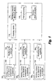
- Fig. 1 a partial view of an exemplary embodiment of the method of manufacturing printed electronic devices in accordance with the disclosure is shown in Fig. 1 and is designated generally by reference character 100.
- One limitation of traditional techniques of using additive manufacturing to manufacture printed electromagnetic devices is the inability to create structures that differ substantially in size, functionality, and accuracy and also can provide the needed material diversity wherein the materials have acceptable properties in comparison to other forming techniques. This is particularly true when attempting to create multicomponent structures in the 3D printing process. For instance, to create a circuit board, both a good electrical conductor and a good nonconductor are required in a pattern.
- Fig. 1 illustrates a method 100 in accordance with the present disclosure for a 3D printing process that effectively manufactures a multicomponent structure while adhering to individual property characteristics and provides improved size compared to traditional techniques.
- the method 100 begins with printing a trace of an electrical component on a substrate at box 102.
- the substrate can belong to the electroactive polymers family, for example, dielectric elastomers.
- Polystyrene is just one example of a family of 'heat shrinkable' materials that are suitable as substrates for use with the methods disclosed herein.
- suitable materials include but are not limited to thermoplastics such as polyolefins, fluoropolymers (e.g.
- the electrical component can include at least one of an electrically conductive, semiconductive, or insulating material.
- the printed trace can be comprised of a metal based ink or a powder.
- the substrate is modified to create a first layer 110 of an electrical device 120.
- the substrate can be modified in varying manners based on the electrical device. For example, the substrate may be shrunk to a target size by heating the substrate at a predetermined temperature for a predetermined duration based on properties of the substrate.
- the substrate can also be modified by curing, cutting and/or etching.
- a subsequent layer or additional layers are created in the same manner at boxes 106 and 108. Although two additional layers are indicated in Fig. 1 , it is to be understood that any suitable number of layers can be used to manufacture the electrical device. For a multicomponent device, this can include additional layers each pertaining to individual electrical components or additional layers with portions of each electrical component embedded therein.
- the first layer 110 and at least one additional layer 106 are assembled or stacked together as shown in box 112. Assembling or stacking the individual layers in this manner allows for printed electronic devices with multiple electronic components for various functionalities.
- electrical component as used and described in the present disclosure includes but is not limited to resistors, capacitors, inductors, transistors, and diodes.
- Electrical device as used and described in the present disclosure, includes a device having one or more electrical components. For example, chemical sensors, radiation sensors, integrated motor coils with embedded sensors and smoke detectors.
- Stacking of the layers may include vertical stacking of each layer. If the substrates are flexible, the stacked layers can be rolled into a cylinder or other 3D form, as needed. In addition, stacking can include interconnecting the layers with an electrical connectivity therebetween.
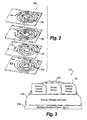
- Fig. 2 illustrates a printed three-dimensional coil 130 manufactured with four layers 132, 134, 136, 138. Through at least three of the layers an electrical interconnector 137 is positioned so as to connect the electrical functionality of each of the four layers 132, 134, 136, 138.
- Modification of the stacked layers may be completed after stacking as needed for specific applications as shown in box 114.
- the stacked layers can be shrunk to a target size by heating the substrate at a predetermined temperature for a predetermined duration based on properties of the substrate.
- Shrinking the layers before and/or after stacking them together provides a multicomponent electrical device that meets design specification for micro, meso and nano-sized circuits.
- stacked layers can be modified by curing, cutting and/or etching.
- the electrical device can then go through post-processing which can include heat treating, coating or the like as in box 116.
- post-processing can include heat treating, coating or the like as in box 116.
- Fig. 3 illustrates an exemplary embodiment of an electronic device 150 that can be manufactured with the methods as described herein.
- the electronic device 150 is a room sensory system with multiple components such as an environmental sensor 152 and a smoke sensor 154. These individual sensors 152, 154 are assembled together with an energy storage and logic component 156. For example a processor and memory can be included in logic component 156. This can be used to alert room occupants as needed based on environmental factors sensed from the sensors 152, 154.
- the components 152, 154, 156 are all electrically connected to a building interface 158 which may supply power to the sensory system 150.
- the sensory system 150 is just one example of an electrical device 120 that can be manufactured with the method 100 as described.
Landscapes
- Engineering & Computer Science (AREA)
- Microelectronics & Electronic Packaging (AREA)
- Chemical & Material Sciences (AREA)
- Manufacturing & Machinery (AREA)
- Dispersion Chemistry (AREA)
- Chemical Kinetics & Catalysis (AREA)
- General Chemical & Material Sciences (AREA)
- Materials Engineering (AREA)
- Mechanical Engineering (AREA)
- Metallurgy (AREA)
- Organic Chemistry (AREA)
- Manufacturing Of Printed Wiring (AREA)
- Parts Printed On Printed Circuit Boards (AREA)
- Manufacturing Cores, Coils, And Magnets (AREA)
Applications Claiming Priority (1)
| Application Number | Priority Date | Filing Date | Title |
|---|---|---|---|
| US201462021571P | 2014-07-07 | 2014-07-07 |
Publications (2)
| Publication Number | Publication Date |
|---|---|
| EP2966945A1 true EP2966945A1 (fr) | 2016-01-13 |
| EP2966945B1 EP2966945B1 (fr) | 2024-02-07 |
Family
ID=53541507
Family Applications (1)
| Application Number | Title | Priority Date | Filing Date |
|---|---|---|---|
| EP15173294.8A Active EP2966945B1 (fr) | 2014-07-07 | 2015-06-23 | Procédé de fabrication de dispositifs électroniques en couches |
Country Status (2)
| Country | Link |
|---|---|
| US (2) | US9832875B2 (fr) |
| EP (1) | EP2966945B1 (fr) |
Cited By (1)
| Publication number | Priority date | Publication date | Assignee | Title |
|---|---|---|---|---|
| WO2017149455A1 (fr) * | 2016-02-29 | 2017-09-08 | King Abdullah University Of Science And Technology | Autocollants électroniques |
Families Citing this family (5)
| Publication number | Priority date | Publication date | Assignee | Title |
|---|---|---|---|---|
| US20150013901A1 (en) * | 2013-07-11 | 2015-01-15 | Hsio Technologies, Llc | Matrix defined electrical circuit structure |
| JP6163702B2 (ja) * | 2014-12-09 | 2017-07-19 | インテル・コーポレーション | パッケージ基板または装置の製造方法 |
| US10126165B2 (en) * | 2015-07-28 | 2018-11-13 | Carrier Corporation | Radiation sensors |
| WO2017171884A1 (fr) * | 2016-04-02 | 2017-10-05 | Intel Corporation | Techniques de formation de caractéristiques fines pour cartes de circuit imprimé |
| US11155023B2 (en) | 2019-01-04 | 2021-10-26 | Rohr, Inc. | Stretching and deployment of a sensor network for large structure monitoring |
Citations (5)
| Publication number | Priority date | Publication date | Assignee | Title |
|---|---|---|---|---|
| GB2180102A (en) * | 1985-09-04 | 1987-03-18 | Grace W R & Co | Heat-miniaturizable printed circuit board |
| US20030146019A1 (en) * | 2001-11-22 | 2003-08-07 | Hiroyuki Hirai | Board and ink used for forming conductive pattern, and method using thereof |
| US20050136231A1 (en) * | 2003-12-18 | 2005-06-23 | 3M Innovative Properties Company | Printed circuits on shrink film |
| US20100112199A1 (en) * | 2005-05-04 | 2010-05-06 | 3M Innovative Properties Company | Microporous article having metallic nanoparticle coating |
| EP2367407A1 (fr) * | 2008-10-30 | 2011-09-21 | Sumitomo Bakelite Co., Ltd. | Substrat de câblage multicouche et son procédé de production |
Family Cites Families (2)
| Publication number | Priority date | Publication date | Assignee | Title |
|---|---|---|---|---|
| US5322594A (en) * | 1993-07-20 | 1994-06-21 | Xerox Corporation | Manufacture of a one piece full width ink jet printing bar |
| US9228859B2 (en) * | 2011-09-26 | 2016-01-05 | Northeastern University | Customizable embedded sensors |
-
2014
- 2014-07-17 US US14/333,856 patent/US9832875B2/en active Active
-
2015
- 2015-06-23 EP EP15173294.8A patent/EP2966945B1/fr active Active
-
2017
- 2017-11-03 US US15/802,676 patent/US20180054894A1/en not_active Abandoned
Patent Citations (5)
| Publication number | Priority date | Publication date | Assignee | Title |
|---|---|---|---|---|
| GB2180102A (en) * | 1985-09-04 | 1987-03-18 | Grace W R & Co | Heat-miniaturizable printed circuit board |
| US20030146019A1 (en) * | 2001-11-22 | 2003-08-07 | Hiroyuki Hirai | Board and ink used for forming conductive pattern, and method using thereof |
| US20050136231A1 (en) * | 2003-12-18 | 2005-06-23 | 3M Innovative Properties Company | Printed circuits on shrink film |
| US20100112199A1 (en) * | 2005-05-04 | 2010-05-06 | 3M Innovative Properties Company | Microporous article having metallic nanoparticle coating |
| EP2367407A1 (fr) * | 2008-10-30 | 2011-09-21 | Sumitomo Bakelite Co., Ltd. | Substrat de câblage multicouche et son procédé de production |
Cited By (1)
| Publication number | Priority date | Publication date | Assignee | Title |
|---|---|---|---|---|
| WO2017149455A1 (fr) * | 2016-02-29 | 2017-09-08 | King Abdullah University Of Science And Technology | Autocollants électroniques |
Also Published As
| Publication number | Publication date |
|---|---|
| US20180054894A1 (en) | 2018-02-22 |
| US20160007462A1 (en) | 2016-01-07 |
| US9832875B2 (en) | 2017-11-28 |
| EP2966945B1 (fr) | 2024-02-07 |
Similar Documents
| Publication | Publication Date | Title |
|---|---|---|
| US20180054894A1 (en) | Method for manufacturing layered electronic devices | |
| CN104851579B (zh) | 印刷电路板和用于制造电感设备的方法 | |
| US8819920B2 (en) | Method of manufacturing stacked resonated coil | |
| EP3211976A1 (fr) | Carte de circuit imprimé avec structure d'antenne et procédé pour sa production | |
| JPWO2016199516A1 (ja) | コイル内蔵多層基板およびその製造方法 | |
| KR101586812B1 (ko) | 연성인쇄회로기판의 제조방법 및 이에 의해 제조된 연성인쇄회로기판 | |
| JP2021532597A (ja) | 誘導素子を製造するための方法及び誘導素子 | |
| US20200047482A1 (en) | Metal objects spanning internal cavities in structures fabricated by additive manufacturing | |
| US10681813B2 (en) | Method for electronics manufacturing using direct write with fabricated foils | |
| CN107437457B (zh) | 一多层电感器及其制造方法 | |
| US20200402712A1 (en) | Multilayered coils | |
| KR20150050306A (ko) | 코일 부품과 그 제조 방법, 코일 부품 내장하는 기판, 및 이를 포함하는 전압조절 모듈 | |
| JP6628007B2 (ja) | 電子部品 | |
| US10225934B2 (en) | Magnetic circuit board and method for manufacturing same | |
| US12142942B2 (en) | Stacked printed circuit board surface in a free-position wireless charger | |
| JP6172214B2 (ja) | 表面実装インダクタの製造方法 | |
| CN209949597U (zh) | 多层基板 | |
| US9570227B1 (en) | Magnetic excitation coil structure | |
| CN109390149B (zh) | 多层式堆叠结构的制作设备以及薄膜电容器的制作方法 | |
| US20170261037A1 (en) | Rolling bearing comprising an electric circuit, and method for producing an electric circuit for a rolling bearing | |
| CN109390151B (zh) | 多层式堆叠结构的制作设备以及薄膜电容器的制作方法 | |
| KR20170097496A (ko) | 인덕터 및 그 제조방법 | |
| US10440845B2 (en) | Electronic transmission controller, and method for producing same | |
| CN201663031U (zh) | 磁性元件 | |
| KR20170087758A (ko) | 인쇄회로기판 |
Legal Events
| Date | Code | Title | Description |
|---|---|---|---|
| PUAI | Public reference made under article 153(3) epc to a published international application that has entered the european phase |
Free format text: ORIGINAL CODE: 0009012 |
|
| AK | Designated contracting states |
Kind code of ref document: A1 Designated state(s): AL AT BE BG CH CY CZ DE DK EE ES FI FR GB GR HR HU IE IS IT LI LT LU LV MC MK MT NL NO PL PT RO RS SE SI SK SM TR |
|
| AX | Request for extension of the european patent |
Extension state: BA ME |
|
| RIN1 | Information on inventor provided before grant (corrected) |
Inventor name: DARDONA, SAMEH Inventor name: CULP, SLADE R. Inventor name: SCHMIDT, WAYDE R. |
|
| 17P | Request for examination filed |
Effective date: 20160713 |
|
| RBV | Designated contracting states (corrected) |
Designated state(s): AL AT BE BG CH CY CZ DE DK EE ES FI FR GB GR HR HU IE IS IT LI LT LU LV MC MK MT NL NO PL PT RO RS SE SI SK SM TR |
|
| STAA | Information on the status of an ep patent application or granted ep patent |
Free format text: STATUS: EXAMINATION IS IN PROGRESS |
|
| 17Q | First examination report despatched |
Effective date: 20190326 |
|
| GRAP | Despatch of communication of intention to grant a patent |
Free format text: ORIGINAL CODE: EPIDOSNIGR1 |
|
| STAA | Information on the status of an ep patent application or granted ep patent |
Free format text: STATUS: GRANT OF PATENT IS INTENDED |
|
| INTG | Intention to grant announced |
Effective date: 20230830 |
|
| RIN1 | Information on inventor provided before grant (corrected) |
Inventor name: SCHMIDT, WAYDE R. Inventor name: DARDONA, SAMEH Inventor name: CULP, SLADE R. |
|
| GRAS | Grant fee paid |
Free format text: ORIGINAL CODE: EPIDOSNIGR3 |
|
| GRAA | (expected) grant |
Free format text: ORIGINAL CODE: 0009210 |
|
| STAA | Information on the status of an ep patent application or granted ep patent |
Free format text: STATUS: THE PATENT HAS BEEN GRANTED |
|
| AK | Designated contracting states |
Kind code of ref document: B1 Designated state(s): AL AT BE BG CH CY CZ DE DK EE ES FI FR GB GR HR HU IE IS IT LI LT LU LV MC MK MT NL NO PL PT RO RS SE SI SK SM TR |
|
| REG | Reference to a national code |
Ref country code: GB Ref legal event code: FG4D |
|
| REG | Reference to a national code |
Ref country code: CH Ref legal event code: EP |
|
| REG | Reference to a national code |
Ref country code: DE Ref legal event code: R096 Ref document number: 602015087464 Country of ref document: DE |
|
| REG | Reference to a national code |
Ref country code: IE Ref legal event code: FG4D |
|
| REG | Reference to a national code |
Ref country code: LT Ref legal event code: MG9D |
|
| REG | Reference to a national code |
Ref country code: NL Ref legal event code: MP Effective date: 20240207 |
|
| PG25 | Lapsed in a contracting state [announced via postgrant information from national office to epo] |
Ref country code: IS Free format text: LAPSE BECAUSE OF FAILURE TO SUBMIT A TRANSLATION OF THE DESCRIPTION OR TO PAY THE FEE WITHIN THE PRESCRIBED TIME-LIMIT Effective date: 20240607 |
|
| PG25 | Lapsed in a contracting state [announced via postgrant information from national office to epo] |
Ref country code: LT Free format text: LAPSE BECAUSE OF FAILURE TO SUBMIT A TRANSLATION OF THE DESCRIPTION OR TO PAY THE FEE WITHIN THE PRESCRIBED TIME-LIMIT Effective date: 20240207 |
|
| PG25 | Lapsed in a contracting state [announced via postgrant information from national office to epo] |
Ref country code: GR Free format text: LAPSE BECAUSE OF FAILURE TO SUBMIT A TRANSLATION OF THE DESCRIPTION OR TO PAY THE FEE WITHIN THE PRESCRIBED TIME-LIMIT Effective date: 20240508 |
|
| REG | Reference to a national code |
Ref country code: AT Ref legal event code: MK05 Ref document number: 1656169 Country of ref document: AT Kind code of ref document: T Effective date: 20240207 |
|
| PG25 | Lapsed in a contracting state [announced via postgrant information from national office to epo] |
Ref country code: HR Free format text: LAPSE BECAUSE OF FAILURE TO SUBMIT A TRANSLATION OF THE DESCRIPTION OR TO PAY THE FEE WITHIN THE PRESCRIBED TIME-LIMIT Effective date: 20240207 Ref country code: RS Free format text: LAPSE BECAUSE OF FAILURE TO SUBMIT A TRANSLATION OF THE DESCRIPTION OR TO PAY THE FEE WITHIN THE PRESCRIBED TIME-LIMIT Effective date: 20240507 Ref country code: NL Free format text: LAPSE BECAUSE OF FAILURE TO SUBMIT A TRANSLATION OF THE DESCRIPTION OR TO PAY THE FEE WITHIN THE PRESCRIBED TIME-LIMIT Effective date: 20240207 |
|
| PG25 | Lapsed in a contracting state [announced via postgrant information from national office to epo] |
Ref country code: ES Free format text: LAPSE BECAUSE OF FAILURE TO SUBMIT A TRANSLATION OF THE DESCRIPTION OR TO PAY THE FEE WITHIN THE PRESCRIBED TIME-LIMIT Effective date: 20240207 |
|
| PG25 | Lapsed in a contracting state [announced via postgrant information from national office to epo] |
Ref country code: AT Free format text: LAPSE BECAUSE OF FAILURE TO SUBMIT A TRANSLATION OF THE DESCRIPTION OR TO PAY THE FEE WITHIN THE PRESCRIBED TIME-LIMIT Effective date: 20240207 |
|
| PG25 | Lapsed in a contracting state [announced via postgrant information from national office to epo] |
Ref country code: RS Free format text: LAPSE BECAUSE OF FAILURE TO SUBMIT A TRANSLATION OF THE DESCRIPTION OR TO PAY THE FEE WITHIN THE PRESCRIBED TIME-LIMIT Effective date: 20240507 Ref country code: NO Free format text: LAPSE BECAUSE OF FAILURE TO SUBMIT A TRANSLATION OF THE DESCRIPTION OR TO PAY THE FEE WITHIN THE PRESCRIBED TIME-LIMIT Effective date: 20240507 Ref country code: NL Free format text: LAPSE BECAUSE OF FAILURE TO SUBMIT A TRANSLATION OF THE DESCRIPTION OR TO PAY THE FEE WITHIN THE PRESCRIBED TIME-LIMIT Effective date: 20240207 Ref country code: LT Free format text: LAPSE BECAUSE OF FAILURE TO SUBMIT A TRANSLATION OF THE DESCRIPTION OR TO PAY THE FEE WITHIN THE PRESCRIBED TIME-LIMIT Effective date: 20240207 Ref country code: IS Free format text: LAPSE BECAUSE OF FAILURE TO SUBMIT A TRANSLATION OF THE DESCRIPTION OR TO PAY THE FEE WITHIN THE PRESCRIBED TIME-LIMIT Effective date: 20240607 Ref country code: HR Free format text: LAPSE BECAUSE OF FAILURE TO SUBMIT A TRANSLATION OF THE DESCRIPTION OR TO PAY THE FEE WITHIN THE PRESCRIBED TIME-LIMIT Effective date: 20240207 Ref country code: GR Free format text: LAPSE BECAUSE OF FAILURE TO SUBMIT A TRANSLATION OF THE DESCRIPTION OR TO PAY THE FEE WITHIN THE PRESCRIBED TIME-LIMIT Effective date: 20240508 Ref country code: FI Free format text: LAPSE BECAUSE OF FAILURE TO SUBMIT A TRANSLATION OF THE DESCRIPTION OR TO PAY THE FEE WITHIN THE PRESCRIBED TIME-LIMIT Effective date: 20240207 Ref country code: ES Free format text: LAPSE BECAUSE OF FAILURE TO SUBMIT A TRANSLATION OF THE DESCRIPTION OR TO PAY THE FEE WITHIN THE PRESCRIBED TIME-LIMIT Effective date: 20240207 Ref country code: BG Free format text: LAPSE BECAUSE OF FAILURE TO SUBMIT A TRANSLATION OF THE DESCRIPTION OR TO PAY THE FEE WITHIN THE PRESCRIBED TIME-LIMIT Effective date: 20240207 Ref country code: AT Free format text: LAPSE BECAUSE OF FAILURE TO SUBMIT A TRANSLATION OF THE DESCRIPTION OR TO PAY THE FEE WITHIN THE PRESCRIBED TIME-LIMIT Effective date: 20240207 |
|
| PG25 | Lapsed in a contracting state [announced via postgrant information from national office to epo] |
Ref country code: PT Free format text: LAPSE BECAUSE OF FAILURE TO SUBMIT A TRANSLATION OF THE DESCRIPTION OR TO PAY THE FEE WITHIN THE PRESCRIBED TIME-LIMIT Effective date: 20240607 Ref country code: PL Free format text: LAPSE BECAUSE OF FAILURE TO SUBMIT A TRANSLATION OF THE DESCRIPTION OR TO PAY THE FEE WITHIN THE PRESCRIBED TIME-LIMIT Effective date: 20240207 |
|
| PG25 | Lapsed in a contracting state [announced via postgrant information from national office to epo] |
Ref country code: SE Free format text: LAPSE BECAUSE OF FAILURE TO SUBMIT A TRANSLATION OF THE DESCRIPTION OR TO PAY THE FEE WITHIN THE PRESCRIBED TIME-LIMIT Effective date: 20240207 Ref country code: PT Free format text: LAPSE BECAUSE OF FAILURE TO SUBMIT A TRANSLATION OF THE DESCRIPTION OR TO PAY THE FEE WITHIN THE PRESCRIBED TIME-LIMIT Effective date: 20240607 Ref country code: PL Free format text: LAPSE BECAUSE OF FAILURE TO SUBMIT A TRANSLATION OF THE DESCRIPTION OR TO PAY THE FEE WITHIN THE PRESCRIBED TIME-LIMIT Effective date: 20240207 Ref country code: LV Free format text: LAPSE BECAUSE OF FAILURE TO SUBMIT A TRANSLATION OF THE DESCRIPTION OR TO PAY THE FEE WITHIN THE PRESCRIBED TIME-LIMIT Effective date: 20240207 |
|
| PG25 | Lapsed in a contracting state [announced via postgrant information from national office to epo] |
Ref country code: DK Free format text: LAPSE BECAUSE OF FAILURE TO SUBMIT A TRANSLATION OF THE DESCRIPTION OR TO PAY THE FEE WITHIN THE PRESCRIBED TIME-LIMIT Effective date: 20240207 |
|
| PG25 | Lapsed in a contracting state [announced via postgrant information from national office to epo] |
Ref country code: SM Free format text: LAPSE BECAUSE OF FAILURE TO SUBMIT A TRANSLATION OF THE DESCRIPTION OR TO PAY THE FEE WITHIN THE PRESCRIBED TIME-LIMIT Effective date: 20240207 |
|
| PG25 | Lapsed in a contracting state [announced via postgrant information from national office to epo] |
Ref country code: EE Free format text: LAPSE BECAUSE OF FAILURE TO SUBMIT A TRANSLATION OF THE DESCRIPTION OR TO PAY THE FEE WITHIN THE PRESCRIBED TIME-LIMIT Effective date: 20240207 Ref country code: CZ Free format text: LAPSE BECAUSE OF FAILURE TO SUBMIT A TRANSLATION OF THE DESCRIPTION OR TO PAY THE FEE WITHIN THE PRESCRIBED TIME-LIMIT Effective date: 20240207 |
|
| PG25 | Lapsed in a contracting state [announced via postgrant information from national office to epo] |
Ref country code: SK Free format text: LAPSE BECAUSE OF FAILURE TO SUBMIT A TRANSLATION OF THE DESCRIPTION OR TO PAY THE FEE WITHIN THE PRESCRIBED TIME-LIMIT Effective date: 20240207 |
|
| PG25 | Lapsed in a contracting state [announced via postgrant information from national office to epo] |
Ref country code: SM Free format text: LAPSE BECAUSE OF FAILURE TO SUBMIT A TRANSLATION OF THE DESCRIPTION OR TO PAY THE FEE WITHIN THE PRESCRIBED TIME-LIMIT Effective date: 20240207 Ref country code: SK Free format text: LAPSE BECAUSE OF FAILURE TO SUBMIT A TRANSLATION OF THE DESCRIPTION OR TO PAY THE FEE WITHIN THE PRESCRIBED TIME-LIMIT Effective date: 20240207 Ref country code: RO Free format text: LAPSE BECAUSE OF FAILURE TO SUBMIT A TRANSLATION OF THE DESCRIPTION OR TO PAY THE FEE WITHIN THE PRESCRIBED TIME-LIMIT Effective date: 20240207 Ref country code: EE Free format text: LAPSE BECAUSE OF FAILURE TO SUBMIT A TRANSLATION OF THE DESCRIPTION OR TO PAY THE FEE WITHIN THE PRESCRIBED TIME-LIMIT Effective date: 20240207 Ref country code: DK Free format text: LAPSE BECAUSE OF FAILURE TO SUBMIT A TRANSLATION OF THE DESCRIPTION OR TO PAY THE FEE WITHIN THE PRESCRIBED TIME-LIMIT Effective date: 20240207 Ref country code: CZ Free format text: LAPSE BECAUSE OF FAILURE TO SUBMIT A TRANSLATION OF THE DESCRIPTION OR TO PAY THE FEE WITHIN THE PRESCRIBED TIME-LIMIT Effective date: 20240207 |
|
| REG | Reference to a national code |
Ref country code: DE Ref legal event code: R097 Ref document number: 602015087464 Country of ref document: DE |
|
| PG25 | Lapsed in a contracting state [announced via postgrant information from national office to epo] |
Ref country code: IT Free format text: LAPSE BECAUSE OF FAILURE TO SUBMIT A TRANSLATION OF THE DESCRIPTION OR TO PAY THE FEE WITHIN THE PRESCRIBED TIME-LIMIT Effective date: 20240207 |
|
| PLBE | No opposition filed within time limit |
Free format text: ORIGINAL CODE: 0009261 |
|
| STAA | Information on the status of an ep patent application or granted ep patent |
Free format text: STATUS: NO OPPOSITION FILED WITHIN TIME LIMIT |
|
| PG25 | Lapsed in a contracting state [announced via postgrant information from national office to epo] |
Ref country code: IT Free format text: LAPSE BECAUSE OF FAILURE TO SUBMIT A TRANSLATION OF THE DESCRIPTION OR TO PAY THE FEE WITHIN THE PRESCRIBED TIME-LIMIT Effective date: 20240207 |
|
| 26N | No opposition filed |
Effective date: 20241108 |
|
| PG25 | Lapsed in a contracting state [announced via postgrant information from national office to epo] |
Ref country code: MC Free format text: LAPSE BECAUSE OF FAILURE TO SUBMIT A TRANSLATION OF THE DESCRIPTION OR TO PAY THE FEE WITHIN THE PRESCRIBED TIME-LIMIT Effective date: 20240207 |
|
| REG | Reference to a national code |
Ref country code: CH Ref legal event code: PL |
|
| PG25 | Lapsed in a contracting state [announced via postgrant information from national office to epo] |
Ref country code: LU Free format text: LAPSE BECAUSE OF NON-PAYMENT OF DUE FEES Effective date: 20240623 |
|
| PG25 | Lapsed in a contracting state [announced via postgrant information from national office to epo] |
Ref country code: IE Free format text: LAPSE BECAUSE OF NON-PAYMENT OF DUE FEES Effective date: 20240623 |
|
| PG25 | Lapsed in a contracting state [announced via postgrant information from national office to epo] |
Ref country code: SI Free format text: LAPSE BECAUSE OF FAILURE TO SUBMIT A TRANSLATION OF THE DESCRIPTION OR TO PAY THE FEE WITHIN THE PRESCRIBED TIME-LIMIT Effective date: 20240207 Ref country code: BE Free format text: LAPSE BECAUSE OF NON-PAYMENT OF DUE FEES Effective date: 20240630 Ref country code: CH Free format text: LAPSE BECAUSE OF NON-PAYMENT OF DUE FEES Effective date: 20240630 |
|
| REG | Reference to a national code |
Ref country code: BE Ref legal event code: MM Effective date: 20240630 |
|
| PGFP | Annual fee paid to national office [announced via postgrant information from national office to epo] |
Ref country code: DE Payment date: 20250520 Year of fee payment: 11 |
|
| PGFP | Annual fee paid to national office [announced via postgrant information from national office to epo] |
Ref country code: GB Payment date: 20250520 Year of fee payment: 11 |
|
| PGFP | Annual fee paid to national office [announced via postgrant information from national office to epo] |
Ref country code: FR Payment date: 20250520 Year of fee payment: 11 |
|
| PG25 | Lapsed in a contracting state [announced via postgrant information from national office to epo] |
Ref country code: CY Free format text: LAPSE BECAUSE OF FAILURE TO SUBMIT A TRANSLATION OF THE DESCRIPTION OR TO PAY THE FEE WITHIN THE PRESCRIBED TIME-LIMIT; INVALID AB INITIO Effective date: 20150623 |
|
| PG25 | Lapsed in a contracting state [announced via postgrant information from national office to epo] |
Ref country code: HU Free format text: LAPSE BECAUSE OF FAILURE TO SUBMIT A TRANSLATION OF THE DESCRIPTION OR TO PAY THE FEE WITHIN THE PRESCRIBED TIME-LIMIT; INVALID AB INITIO Effective date: 20150623 |