EP2973664B1 - Dispositif émetteur d'ultraviolet et procédé pour former un contact sur un dispositif émetteur d'ultraviolet - Google Patents
Dispositif émetteur d'ultraviolet et procédé pour former un contact sur un dispositif émetteur d'ultraviolet Download PDFInfo
- Publication number
- EP2973664B1 EP2973664B1 EP14769060.6A EP14769060A EP2973664B1 EP 2973664 B1 EP2973664 B1 EP 2973664B1 EP 14769060 A EP14769060 A EP 14769060A EP 2973664 B1 EP2973664 B1 EP 2973664B1
- Authority
- EP
- European Patent Office
- Prior art keywords
- layer
- light
- emitting device
- contact
- cap layer
- Prior art date
- Legal status (The legal status is an assumption and is not a legal conclusion. Google has not performed a legal analysis and makes no representation as to the accuracy of the status listed.)
- Active
Links
Images

Classifications
-
- H—ELECTRICITY
- H10—SEMICONDUCTOR DEVICES; ELECTRIC SOLID-STATE DEVICES NOT OTHERWISE PROVIDED FOR
- H10H—INORGANIC LIGHT-EMITTING SEMICONDUCTOR DEVICES HAVING POTENTIAL BARRIERS
- H10H20/00—Individual inorganic light-emitting semiconductor devices having potential barriers, e.g. light-emitting diodes [LED]
- H10H20/01—Manufacture or treatment
- H10H20/011—Manufacture or treatment of bodies, e.g. forming semiconductor layers
- H10H20/013—Manufacture or treatment of bodies, e.g. forming semiconductor layers having light-emitting regions comprising only Group III-V materials
- H10H20/0137—Manufacture or treatment of bodies, e.g. forming semiconductor layers having light-emitting regions comprising only Group III-V materials the light-emitting regions comprising nitride materials
-
- H—ELECTRICITY
- H10—SEMICONDUCTOR DEVICES; ELECTRIC SOLID-STATE DEVICES NOT OTHERWISE PROVIDED FOR
- H10H—INORGANIC LIGHT-EMITTING SEMICONDUCTOR DEVICES HAVING POTENTIAL BARRIERS
- H10H20/00—Individual inorganic light-emitting semiconductor devices having potential barriers, e.g. light-emitting diodes [LED]
- H10H20/80—Constructional details
- H10H20/81—Bodies
- H10H20/811—Bodies having quantum effect structures or superlattices, e.g. tunnel junctions
- H10H20/812—Bodies having quantum effect structures or superlattices, e.g. tunnel junctions within the light-emitting regions, e.g. having quantum confinement structures
-
- H—ELECTRICITY
- H10—SEMICONDUCTOR DEVICES; ELECTRIC SOLID-STATE DEVICES NOT OTHERWISE PROVIDED FOR
- H10H—INORGANIC LIGHT-EMITTING SEMICONDUCTOR DEVICES HAVING POTENTIAL BARRIERS
- H10H20/00—Individual inorganic light-emitting semiconductor devices having potential barriers, e.g. light-emitting diodes [LED]
- H10H20/80—Constructional details
- H10H20/81—Bodies
- H10H20/815—Bodies having stress relaxation structures, e.g. buffer layers
-
- H—ELECTRICITY
- H10—SEMICONDUCTOR DEVICES; ELECTRIC SOLID-STATE DEVICES NOT OTHERWISE PROVIDED FOR
- H10H—INORGANIC LIGHT-EMITTING SEMICONDUCTOR DEVICES HAVING POTENTIAL BARRIERS
- H10H20/00—Individual inorganic light-emitting semiconductor devices having potential barriers, e.g. light-emitting diodes [LED]
- H10H20/80—Constructional details
- H10H20/81—Bodies
- H10H20/816—Bodies having carrier transport control structures, e.g. highly-doped semiconductor layers or current-blocking structures
-
- H—ELECTRICITY
- H10—SEMICONDUCTOR DEVICES; ELECTRIC SOLID-STATE DEVICES NOT OTHERWISE PROVIDED FOR
- H10H—INORGANIC LIGHT-EMITTING SEMICONDUCTOR DEVICES HAVING POTENTIAL BARRIERS
- H10H20/00—Individual inorganic light-emitting semiconductor devices having potential barriers, e.g. light-emitting diodes [LED]
- H10H20/80—Constructional details
- H10H20/81—Bodies
- H10H20/819—Bodies characterised by their shape, e.g. curved or truncated substrates
- H10H20/82—Roughened surfaces, e.g. at the interface between epitaxial layers
-
- H—ELECTRICITY
- H10—SEMICONDUCTOR DEVICES; ELECTRIC SOLID-STATE DEVICES NOT OTHERWISE PROVIDED FOR
- H10H—INORGANIC LIGHT-EMITTING SEMICONDUCTOR DEVICES HAVING POTENTIAL BARRIERS
- H10H20/00—Individual inorganic light-emitting semiconductor devices having potential barriers, e.g. light-emitting diodes [LED]
- H10H20/80—Constructional details
- H10H20/81—Bodies
- H10H20/822—Materials of the light-emitting regions
- H10H20/824—Materials of the light-emitting regions comprising only Group III-V materials, e.g. GaP
- H10H20/825—Materials of the light-emitting regions comprising only Group III-V materials, e.g. GaP containing nitrogen, e.g. GaN
-
- H—ELECTRICITY
- H10—SEMICONDUCTOR DEVICES; ELECTRIC SOLID-STATE DEVICES NOT OTHERWISE PROVIDED FOR
- H10H—INORGANIC LIGHT-EMITTING SEMICONDUCTOR DEVICES HAVING POTENTIAL BARRIERS
- H10H20/00—Individual inorganic light-emitting semiconductor devices having potential barriers, e.g. light-emitting diodes [LED]
- H10H20/80—Constructional details
- H10H20/81—Bodies
- H10H20/822—Materials of the light-emitting regions
- H10H20/824—Materials of the light-emitting regions comprising only Group III-V materials, e.g. GaP
- H10H20/825—Materials of the light-emitting regions comprising only Group III-V materials, e.g. GaP containing nitrogen, e.g. GaN
- H10H20/8252—Materials of the light-emitting regions comprising only Group III-V materials, e.g. GaP containing nitrogen, e.g. GaN characterised by the dopants
-
- H—ELECTRICITY
- H10—SEMICONDUCTOR DEVICES; ELECTRIC SOLID-STATE DEVICES NOT OTHERWISE PROVIDED FOR
- H10H—INORGANIC LIGHT-EMITTING SEMICONDUCTOR DEVICES HAVING POTENTIAL BARRIERS
- H10H20/00—Individual inorganic light-emitting semiconductor devices having potential barriers, e.g. light-emitting diodes [LED]
- H10H20/80—Constructional details
- H10H20/83—Electrodes
- H10H20/832—Electrodes characterised by their material
-
- H—ELECTRICITY
- H10—SEMICONDUCTOR DEVICES; ELECTRIC SOLID-STATE DEVICES NOT OTHERWISE PROVIDED FOR
- H10H—INORGANIC LIGHT-EMITTING SEMICONDUCTOR DEVICES HAVING POTENTIAL BARRIERS
- H10H20/00—Individual inorganic light-emitting semiconductor devices having potential barriers, e.g. light-emitting diodes [LED]
- H10H20/80—Constructional details
- H10H20/83—Electrodes
- H10H20/832—Electrodes characterised by their material
- H10H20/835—Reflective materials
-
- H—ELECTRICITY
- H10—SEMICONDUCTOR DEVICES; ELECTRIC SOLID-STATE DEVICES NOT OTHERWISE PROVIDED FOR
- H10H—INORGANIC LIGHT-EMITTING SEMICONDUCTOR DEVICES HAVING POTENTIAL BARRIERS
- H10H20/00—Individual inorganic light-emitting semiconductor devices having potential barriers, e.g. light-emitting diodes [LED]
- H10H20/80—Constructional details
- H10H20/84—Coatings, e.g. passivation layers or antireflective coatings
- H10H20/841—Reflective coatings, e.g. dielectric Bragg reflectors
-
- H—ELECTRICITY
- H10—SEMICONDUCTOR DEVICES; ELECTRIC SOLID-STATE DEVICES NOT OTHERWISE PROVIDED FOR
- H10H—INORGANIC LIGHT-EMITTING SEMICONDUCTOR DEVICES HAVING POTENTIAL BARRIERS
- H10H20/00—Individual inorganic light-emitting semiconductor devices having potential barriers, e.g. light-emitting diodes [LED]
- H10H20/80—Constructional details
- H10H20/85—Packages
- H10H20/855—Optical field-shaping means, e.g. lenses
- H10H20/856—Reflecting means
-
- H—ELECTRICITY
- H10—SEMICONDUCTOR DEVICES; ELECTRIC SOLID-STATE DEVICES NOT OTHERWISE PROVIDED FOR
- H10H—INORGANIC LIGHT-EMITTING SEMICONDUCTOR DEVICES HAVING POTENTIAL BARRIERS
- H10H20/00—Individual inorganic light-emitting semiconductor devices having potential barriers, e.g. light-emitting diodes [LED]
- H10H20/01—Manufacture or treatment
- H10H20/032—Manufacture or treatment of electrodes
-
- H—ELECTRICITY
- H10—SEMICONDUCTOR DEVICES; ELECTRIC SOLID-STATE DEVICES NOT OTHERWISE PROVIDED FOR
- H10H—INORGANIC LIGHT-EMITTING SEMICONDUCTOR DEVICES HAVING POTENTIAL BARRIERS
- H10H20/00—Individual inorganic light-emitting semiconductor devices having potential barriers, e.g. light-emitting diodes [LED]
- H10H20/01—Manufacture or treatment
- H10H20/034—Manufacture or treatment of coatings
-
- H—ELECTRICITY
- H10—SEMICONDUCTOR DEVICES; ELECTRIC SOLID-STATE DEVICES NOT OTHERWISE PROVIDED FOR
- H10H—INORGANIC LIGHT-EMITTING SEMICONDUCTOR DEVICES HAVING POTENTIAL BARRIERS
- H10H20/00—Individual inorganic light-emitting semiconductor devices having potential barriers, e.g. light-emitting diodes [LED]
- H10H20/01—Manufacture or treatment
- H10H20/036—Manufacture or treatment of packages
- H10H20/0363—Manufacture or treatment of packages of optical field-shaping means
-
- H—ELECTRICITY
- H10—SEMICONDUCTOR DEVICES; ELECTRIC SOLID-STATE DEVICES NOT OTHERWISE PROVIDED FOR
- H10H—INORGANIC LIGHT-EMITTING SEMICONDUCTOR DEVICES HAVING POTENTIAL BARRIERS
- H10H20/00—Individual inorganic light-emitting semiconductor devices having potential barriers, e.g. light-emitting diodes [LED]
- H10H20/80—Constructional details
- H10H20/81—Bodies
- H10H20/811—Bodies having quantum effect structures or superlattices, e.g. tunnel junctions
-
- H—ELECTRICITY
- H10—SEMICONDUCTOR DEVICES; ELECTRIC SOLID-STATE DEVICES NOT OTHERWISE PROVIDED FOR
- H10H—INORGANIC LIGHT-EMITTING SEMICONDUCTOR DEVICES HAVING POTENTIAL BARRIERS
- H10H20/00—Individual inorganic light-emitting semiconductor devices having potential barriers, e.g. light-emitting diodes [LED]
- H10H20/80—Constructional details
- H10H20/83—Electrodes
- H10H20/831—Electrodes characterised by their shape
- H10H20/8316—Multi-layer electrodes comprising at least one discontinuous layer
-
- H—ELECTRICITY
- H10—SEMICONDUCTOR DEVICES; ELECTRIC SOLID-STATE DEVICES NOT OTHERWISE PROVIDED FOR
- H10H—INORGANIC LIGHT-EMITTING SEMICONDUCTOR DEVICES HAVING POTENTIAL BARRIERS
- H10H20/00—Individual inorganic light-emitting semiconductor devices having potential barriers, e.g. light-emitting diodes [LED]
- H10H20/80—Constructional details
- H10H20/83—Electrodes
- H10H20/832—Electrodes characterised by their material
- H10H20/833—Transparent materials
Definitions
- the present invention relates to improving carrier injection efficiency (e.g., the hole injection efficiency) into high-aluminum-content ultraviolet light-emitting devices.
- Embodiments of the present invention also relate to improving ultraviolet light-emitting devices fabricated on nitride-based substrates, in particular to improving light extraction therefrom.
- UV LEDs ultraviolet light-emitting diodes
- LEDs that emit light at wavelengths less than 350 nm - based on the nitride semiconductor system remain limited due to high defect levels in the active region.
- These limitations are particularly problematic (and notable) in devices designed to emit at wavelengths less than 280 nm.
- defect densities remain high despite significant efforts to reduce them. These high defect densities limit both the efficiency and the reliability of devices grown on such substrates.
- AlN crystalline aluminum nitride
- these pseudomorphic UV LEDs are mounted for packaging in a "flip-chip" configuration, where the light generated in the active region of the device is emitted through the AlN substrate, while the LED dies have their front surfaces (i.e., the top surfaces of the devices during epitaxial growth and initial device fabrication prior to bonding) bonded to a patterned submount which is used to make electrical and thermal contact to the LED chip.
- a good submount material is polycrystalline (ceramic) AlN because of the relatively good thermal expansion match with the AlN chip and because of the high thermal conductivity of this material. Due to the high crystalline perfection that is achievable in the active device region of such devices, internal efficiencies greater than 60% have been demonstrated.
- the photon-extraction efficiency is often still very poor in these devices, ranging from about 4% to about 15% achieved using surface-patterning techniques - much lower than exhibited by many visible-light (or "visible") LEDs.
- the current generation of short-wavelength UV LEDs has low wall-plug efficiencies (WPEs) of, at best, only a few percent, where the WPE is defined as the ratio of usable optical power (in this case, emitted UV light) achieved from the diode to the electrical power supplied into the device.
- UV LEDs typically suffer because approximately 50% of the generated photons are directed toward the p-contact, which typically includes photon-absorbing p-GaN. Even when photons are directed toward the AlN surface, only about 9.4% typically escape from an untreated surface due to the large index of refraction of the AlN, which results in a small escape cone. These losses are multiplicative and the average photon extraction efficiency may be quite low.
- Grandusky 2013 As demonstrated in a recent publication by Grandusky et al. ( James R. Grandusky et al., 2013 Appl. Phys. Express, Vol. 6, No. 3, 032101 , hereinafter referred to as "Grandusky 2013"), it is possible to increase the photon extraction efficiency to approximately 15% in pseudomorphic UV LEDs grown on AlN substrates via the attachment of an inorganic (and typically rigid) lens directly to the LED die via a thin layer of an encapsulant (e.g., an organic, UV-resistant encapsulant compound).
- an encapsulant e.g., an organic, UV-resistant encapsulant compound
- the photon extraction efficiency may be increased by thinning the AlN substrate and by roughening the surface of the AlN substrate surface as discussed in the '833 patent.
- p-GaN is utilized conventionally because it is very difficult to make a low-resistivity contact to p-Al x Ga 1-x N where x is greater than 0.3.
- metals that allow low-resistivity contact to the p-type nitride semiconductor material are generally poor reflectors. This reflectivity problem is particularly exacerbated when the desired wavelength of the LED is less than 340 nm since most common metals will start to absorb strongly in that regime.
- the above-referenced shortcomings might be remedied via the use of a non-absorbing p-type semiconductor on the p-side of the LED and the use of p-contact metallurgy that reflects the UV photons.
- conventional approaches are unsuited to pseudomorphic UV LEDs since these approaches use multiple layers of thin p-Al x Ga 1-x N where the p-type Al x Ga 1-x N layers are thin enough to be optically transparent to the UV radiation at wavelengths shorter than 300 nm.
- This type of multi-layer structure is very difficult to grow on a pseudomorphic device structure (where the underlying substrate is either AlN or Al x Ga 1-x N with x>0.6), because the large amount of strain (due to the lattice mismatch) typically causes the thin GaN (or low aluminum content Al x Ga 1-x N) to island and become very rough.
- contact roughening is addressed by making the p-type GaN layer quite thick; however, such layers, as detailed above, absorb UV photons and diminish UV LED device efficiencies.
- the present invention provides a method of forming a contact to an ultraviolet light-emitting device in accordance with the appended claim 1.
- the present invention also provides an ultraviolet light-emitting device in accordance with the appended claim 6.
- a smooth p-GaN (or p-Al x Ga 1-x N layer where x ⁇ 0.3) layer is produced on the active region (e.g., a pseudomorphic active region) of an ultraviolet light-emitting device grown on a single-crystal AlN substrate or single-crystal Al x Ga 1-x N substrate where x>0.6.
- This smooth p-GaN or p-Al x Ga 1-x N layer where x ⁇ 0.3 will hereinafter be abbreviated as the SPG layer.
- the SPG layer is very desirable for improved fabrication of any pseudomorphic electronic or optoelectronic device utilizing a p-contact because it minimizes or substantially eliminates the rough surfaces that are difficult to etch and metallize uniformly.
- the SPG layer may also be made sufficiently thin to be transparent to UV radiation having wavelengths shorter than 340 nm.
- the thin, UV-transparent SPG layer may be combined with a reflective metal contact to the SPG layer, and this bilayer structure may then be used to both efficiently inject holes into a UV optoelectronic device and reflect UV photons from the p-contact.
- the thin, UV-transparent SPG layer when combined with an appropriately designed UV reflective contact, will allow a pseudomorphic UV LED to be fabricated on an AlN (or Al x Ga 1-x N substrate with x>0.6) substrate with a photon extraction efficiency greater than 25%.
- the thin SPG layer on a pseudomorphic UV LED may be combined with a reflector metal contact to achieve a WPE greater than 10% at wavelengths shorter than 275 nm at current densities exceeding 30 A/cm 2 .
- a first metal layer capable of making a low-resistivity contact to the SPG layer is disposed on the SPG layer and patterned.
- the resulting gaps in the first metal layer may then be filled via the deposition of a second metal layer that is an efficient reflector of UV photons.
- the two-metal structure provides the dual advantages of low contact resistance and high reflectivity, both of which improve the performance of UV LEDs.
- Al may be used as the reflector metal, as it has >90% reflectivity to light having a wavelength of approximately 265 nm.
- Al is quite poor for making a low-resistivity contact to p-type GaN or p-type Al x Ga 1-x N because of its low work function (4.26 eV).
- the high resistivity of the Al/nitride interface is addressed by the regions of the low-resistivity contact metal; however, in order to prevent absorption of the UV photons by the contact metal, preferred embodiments of the invention utilize only limited contact areas between the contact metal and the underlying semiconductor rather than a contact metal-semiconductor contact area covering substantially all of the semiconductor surface.
- the contact metal in some embodiments (i) more than about 10% of the semiconductor surface is covered by the contact metal, but (ii) less than about 70%, less than about 60%, less than about 50%, or even less than 40% of the semiconductor surface is covered by the contact metal, while the remaining portion of the semiconductor surface is covered by the reflector metal to minimize deleterious absorption of the UV light.
- embodiments of the invention feature a method of forming a contact to a UV light-emitting device.
- a substrate having an Al y Ga 1-y N top surface is provided, where y ⁇ 0.4 (and ⁇ 1.0).
- the substrate may be substantially entirety composed of the Al y Ga 1-y N material (e.g., AlN), or the substrate may include or consist essentially of a different material (e.g., silicon carbide, silicon, and/or sapphire) with the Al y Ga 1-y N material formed thereover by e.g., epitaxial growth; such material may be substantially fully lattice relaxed and may have a thickness of, e.g., at least 1 ⁇ m.
- An active, light-emitting device structure is formed over the substrate, the device structure including or consisting essentially of a plurality of layers each including or consisting essentially of Al x Ga 1-x N.
- An undoped graded Al 1-z Ga z N layer is formed over the device structure, a composition of the graded layer being graded in Ga concentration z such that the Ga concentration z increases in a direction away from the light-emitting device structure.
- the Ga concentration z may increase from a composition of approximately 0.15 proximate the device structure to a composition of approximately 1 at the top of the graded layer.
- a p-doped Al 1-w Ga w N cap layer is formed over the graded layer, the cap layer (i) having a thickness between 2 nm and 30 nm, (ii) a surface roughness of less than 6 nm over a sample size of 200 ⁇ m x 300 ⁇ m, and (iii) a Ga concentration w ⁇ 0.8.
- a metallic contact comprising a least one metal is formed over the Al 1-w Ga w N cap layer, the metallic contact having a contact resistivity to the Al 1-w Ga w N cap layer of less than 1.0 m ⁇ -cm 2 .
- Embodiments of the invention may include one or more of the following in any of a variety of combinations.
- Forming the Al 1-w Ga w N cap layer may include or consist of epitaxial growth at a temperature between 850°C and 900°C and a growth pressure less than 50 Torr, e.g., between approximately 10 Torr and approximately 30 Torr, for example 20 Torr.
- the Al 1-w Ga w N cap layer may be doped with Mg and/or may be at least partially relaxed.
- the light-emitting device may have a photon extraction efficiency of greater than 25%.
- the graded layer and Al 1-w Ga w N cap layer may collectively absorb less than 80% of UV photons generated by the light-emitting device structure and having a wavelength less than 340 nm.
- the at least one metal of the metallic contact may include or consist of Ni/Au and/or Pd.
- the metallic contact may have a reflectivity to light generated by the light-emitting device structure of 60% or less, or even 30% or less.
- the metallic contact may be formed as a plurality of discrete lines and/or pixels of the at least one metal, portions of the Al 1-w Ga w N cap layer not being covered by the metallic contact.
- a reflector may be formed over the metallic contact and the uncovered portions of the Al 1-w Ga w N cap layer.
- the reflector may include or consist of a metal having greater than 60%, or even greater than 90%, reflectivity to UV light and a work function less than 4.5 eV.
- the reflector may have a contact resistivity to the Al 1-w Ga w N cap layer of greater than approximately 5 m ⁇ -cm 2 , or even greater than approximately 10 m ⁇ -cm 2 .
- the reflector may include or consist of Al.
- the UV light-emitting device may include or consist essentially of a light-emitting diode or a laser.
- a bottom portion of the graded layer proximate the active device structure may have a Ga concentration z equal to a Ga concentration of a layer directly thereunder, and/or a top portion of the graded layer opposite the bottom portion of the graded layer may have a Ga concentration z of 1.
- Forming the Al 1-w Ga w N cap layer may include or consist essentially of epitaxial growth at a growth rate between 0.5 nm/min and 5 nm/min.
- a surface of the graded layer may be exposed to a precursor of the p-type dopant of the cap layer without exposure to a Ga precursor.
- the p-type dopant of the cap layer may include or consist of Mg.
- the substrate may consist of doped or undoped AlN.
- embodiments of the invention feature a UV light-emitting device including or consisting essentially of a substrate having an Al y Ga 1-y N top surface, where y ⁇ 0.4 (and ⁇ 1.0), an active light-emitting device structure disposed over the substrate, the device structure including or consisting of a plurality of layers each including or consisting of Al x Ga 1-x N, an undoped graded Al 1-z Ga z N layer disposed over the device structure, a composition of the graded layer being graded in Ga concentration z such that the Ga concentration z increases in a direction away from the light-emitting device structure, a p-doped Al 1-w Ga w N cap layer disposed over the graded layer, the p-doped Al 1-w Ga w N cap layer (i) having a thickness between 2 nm and 30 nm, (ii) a surface roughness of less than 6 nm over a sample size of 200 ⁇
- the substrate may be substantially entirely composed of the Al y Ga 1-y N material (e.g., AlN), or the substrate may include or consist essentially of a different material (e.g., silicon carbide, silicon, and/or sapphire) with the Al y Ga 1-y N material formed thereover by e.g., epitaxial growth; such material may be substantially fully lattice relaxed and may have a thickness of, e.g., at least 1 ⁇ m.
- a different material e.g., silicon carbide, silicon, and/or sapphire
- Embodiments of the invention may include one or more of the following in any of a variety of combinations.
- the Al 1-w Ga w N cap layer may be doped with Mg and/or may be at least partially relaxed.
- the light-emitting device may have a photon extraction efficiency of greater than 25%.
- the graded layer and Al 1-w Ga w N cap layer may collectively absorb less than 80% of UV photons generated by the light-emitting device structure and having a wavelength less than 340 nm.
- the at least one metal of the metallic contact may include or consist of Ni/Au and/or Pd.
- the metallic contact may have reflectivity to light generated by the light-emitting device structure of 60% or less, or even 30% or less.
- the metallic contact may have the form of a plurality of discrete lines and/or pixels of the at least one metal, portions of the Al 1-w Ga w N cap layer not being covered by the metallic contact.
- a reflector may be disposed over the metallic contact and the uncovered portions of the Al 1-w Ga w N cap layer.
- the reflector may include or consist of a metal having greater than 5 m ⁇ -cm 2 , or even greater than 10 m ⁇ -cm 2 .
- the reflector may include or consist of Al.
- the light-emitting device may include or consist essentially of a light-emitting diode or a laser.
- a bottom portion of the graded layer proximate the active device structure may have a Ga concentration z equal to a Ga concentration of a layer directly thereunder, and/or a top portion of the graded layer opposite the bottom portion of the graded layer may have a Ga concentration z of 1.
- the substrate may consist of doped or undoped AlN.
- Embodiments of the invention include pseudomorphic Al x Ga 1-x N UV light-emitting devices on a substrate having an Al y Ga 1-y N top surface, where y ⁇ 0.4 (and ⁇ 1.0).
- the substrate may be substantially entirely composed of the Al y Ga 1-y N material (e.g., AlN), or the substrate may include or consist essentially of a different material (e.g., silicon carbide, silicon, and/or sapphire) with the Al y Ga 1-y N material formed thereover by e.g., epitaxial growth; such material may be substantially fully lattice relaxed and may have a thickness of, e.g., at least 1 ⁇ m.
- the substrate need not be transparent to UV radiation (e.g., silicon), since it may be partially or substantially removed during device fabrication.)
- the UV light-emitting devices according to embodiments of the invention also have a thin p-GaN or p-Al x Ga 1-x N contact layer that is smooth (i.e., having a root-mean-square (Rq) surface roughness of less than 6 nm, or even less than approximately 1 nm). The roughness may be characterized with optical profilometry over a sample size of approximately 200 ⁇ m ⁇ 300 ⁇ m, e.g., 233 ⁇ m ⁇ 306.5 ⁇ m.
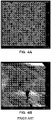
- Figure 1 depicts a profilometry scan of a conventional rough contact-layer surface having an Rq value of approximately 33 nm.
- Figure 2 depicts a smooth contact surface in accordance with embodiments of the present invention that has an Rq value of only approximately 6 nm.
- the threading dislocation density (TDD) in the active region of the device is less than 10 5 cm -2 .
- the thin p-GaN or p-Al x Ga 1-x N (SPG) final layer will be sufficiently thin to allow light with wavelengths shorter than 340 nm to be transmitted with minimal absorption (i.e., absorption in a single pass no greater than 80%, no greater than 50%, or even no greater than 40%).
- the UV absorption at wavelengths shorter than 340 nm may be decreased to 50%, to 25%, to 10%, or even to 5% or less.
- Table 1 illustrates various thickness-absorption relationships for Al x Ga 1-x N layers of various Al contents x and thicknesses for a variety of emission wavelengths. In Table 1, absorption values are shown for layers of 40% Al only for emission wavelengths up to 265 nm, as such layers become substantially transparent at larger wavelengths.
- a UV reflector may be introduced into the device structure to reflect transmitted photons and direct them towards the AlN substrate so that they may be extracted from the device.
- visible LEDs this is often accomplished by using a silver p-contact, as silver both forms an ohmic contact to visible-LED structures and is reflective to visible photons.
- the layers that form a visible LED are generally transparent to the photons being generated in the quantum wells.
- the reflectivity of silver drops rapidly in the UV range. The reflectivities of most other common metals also drop as the wavelength decreases into the UV range with the exception of Al, which unfortunately does not form a good ohmic contact to p-type GaN or Al x Ga 1-x N.
- a fairly non-reflective (at least to UV photons) contact metallurgy (e.g., Ni/Au or Pd) may be formed over the contact layer but patterned to reduce the surface "footprint" of the contact over the semiconductor. In this manner, the surface area over the device layers that is non-reflective to UV photons is minimized, yet good ohmic contact to the semiconductor is still achieved.
- a reflective metal such as Al may be provided directly over the semiconductor between the non-reflective contact regions. The reflective metal makes an ohmic contact with the non-reflective metal, enabling electrical contact to the LED while utilizing the superior metal-semiconductor contact formed by the non-reflective metal.
- the SPG layer may include or consist essentially of a p-GaN or p-Al x Ga 1-x N layer where x ⁇ 0.3.
- thicker SPG layers may be utilized as the Ga content is decreased, as the lattice-mismatch strain (that may roughen the SPG layer) between the SPG layer and the underlying AlN substrate decreases.
- the Ga content of the SPG layer is preferably maintained at or above 70% in order to enable a highly doped, low-resistivity layer.
- the activation energy of the Mg impurity is increased. This leads to lower activation of the Mg, resulting in lower hole concentration as the Al mole fraction is increased.
- One solution to this is to utilize polarization-induced doping, which may be achieved by the grading of an Al x Ga 1-x N layer from high x to lower x as it is deposited. This may be used to achieve hole concentrations much higher than may be achieved through conventional impurity doping. In addition, this technique may result in improved carrier mobilities due to lack of impurity scattering and reduced temperature dependence of the hole concentration.
- High hole concentrations may be achieved in the absence of impurity doping or in addition to impurity doping.
- Preferred embodiments of the invention feature low dislocation density in pseudomorphic graded layers, which enables high hole concentration in the absence of impurity doping, thus allowing for higher conductivity and improved current spreading from thin transparent layers. These high hole concentrations make it possible to achieve p-contacts with low resistivity.
- resistivities less than 10 m ⁇ -cm 2 may be achieved in accordance with embodiments of the present invention. In preferred embodiments, resistivities less than 5 m ⁇ -cm 2 are achieved and utilized in UV LEDs.
- the device may be operated at 30A/cm 2 with a 1:3 ratio of contact metal to reflector metal (as detailed above) and achieve a voltage drop across the p-contact of less than 1.2 V with a device area of 0.0033 cm 2 .
- a 1:3 ratio of contact metal to reflector metal as detailed above
- the device may be operated at 30A/cm 2 with a 1:3 ratio of contact metal to reflector metal (as detailed above) and achieve a voltage drop across the p-contact of less than 1.2 V with a device area of 0.0033 cm 2 .
- embodiments of the invention exhibit wall plug efficiencies greater than 10% at an operating current density exceeding 30 A/cm 2 .
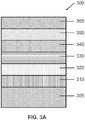
- FIG. 3A depicts a pseudomorphic UV light emitting diode (“PUVLED”) structure 300 in accordance with embodiments of the present invention.
- a semiconductor substrate 305 which includes or consists of a substrate having an Al y Ga 1-y N top surface, where y ⁇ 0.4 (and ⁇ 1.0), is provided.
- the substrate may be substantially entirely composed of the Al y Ga 1-y N material (e.g., AlN), or the substrate may include or consist essentially of a different material (e.g., silicon carbide, silicon, and/or sapphire) with the Al y Ga 1-y N material formed thereover by e.g., epitaxial growth; such material may be substantially fully lattice relaxed and may have a thickness of, e.g., at least 1 ⁇ m.
- the substrate 305 need not be transparent to UV radiation (e.g., silicon), since it may be partially or substantially removed during device fabrication.
- Semiconductor substrate 305 may be miscut such that the angle between its c-axis and its surface normal is between approximately 0° and approximately 4°.
- the misorientation of the surface of semiconductor substrate 305 is less than approximately 0.3°, e.g., for semiconductor substrates 305 that are not deliberately or controllably miscut. In other embodiments, the misorientation of the surface of semiconductor substrate 305 is greater than approximately 0.3°, e.g., for semiconductor substrates 305 that are deliberately and controllably miscut. In a preferred embodiment, the direction of the miscut is towards the a-axis.
- the surface of semiconductor substrate 305 may have a group-III (e.g., Al-) polarity or N-polarity, and may be planarized, e.g., by chemical-mechanical polishing.
- the RMS surface roughness of semiconductor substrate is preferably less than approximately 0.5 nm for a 10 ⁇ m ⁇ 10 ⁇ m area.
- atomic-level steps are detectable on the surface when probed with an atomic-force microscope.
- the threading dislocation density of semiconductor substrate 305 may be measured using, e.g., etch pit density measurements after a 5 minute KOH-NaOH eutectic etch at 450 °C.
- the threading dislocation density is less than approximately 2 ⁇ 10 3 cm -2 .
- substrate 305 has an even lower threading dislocation density.
- Semiconductor substrate 305 may be topped with a homoepitaxial layer (not shown) that includes or consists essentially of the same semiconductor material present in semiconductor substrate 300, e.g., AlN.
- an optional graded buffer layer 310 is formed on semiconductor substrate 305.
- Graded buffer layer 310 may include or consist essentially of one or more semiconductor materials, e.g., Al x Ga 1-x N.
- graded buffer layer 310 has a composition approximately equal to that of semiconductor substrate 305 at an interface therewith in order to promote two-dimensional growth and avoid deleterious islanding (such islanding may result in undesired elastic strain relief and/or surface roughening in graded buffer layer 310 and subsequently grown layers).
- graded buffer layer 310 at an interface with subsequently grown layers is generally chosen to be close to (e.g., approximately equal to) that of the desired active region of the device (e.g., the Al x Ga 1-x N concentration that will result in the desired wavelength emission from the PUVLED).
- graded buffer layer 310 includes Al x Ga 1-x N graded from an Al concentration x of approximately 100% to an Al concentration x of approximately 60%.
- a bottom contact layer 320 is subsequently formed above substrate 305 and optional graded buffer layer 310, and may include or consist essentially of Al x Ga 1-x N doped with at least one impurity, e.g., Si.
- the Al concentration x in bottom contact layer 320 is approximately equal to the final Al concentration x in graded layer 310 (i.e., approximately equal to that of the desired active region (described below) of the device).
- Bottom contact layer 320 may have a thickness sufficient to prevent current crowding after device fabrication (as described below) and/or to stop on during etching to fabricate contacts.
- the thickness of bottom contact layer 320 may be less than approximately 200 nm.
- bottom contact layer 320 When utilizing a bottom contact layer 320 of such thickness, the final PUVLED may be fabricated with backside contacts.
- bottom contact layer 320 will have high electrical conductivity even with a small thickness due to the low defect density maintained when the layer is pseudomorphic.
- a pseudomorphic film is one where the strain parallel to the interface is approximately that needed to distort the lattice in the film to match that of the substrate.
- the parallel strain in a pseudomorphic film will be nearly or approximately equal to the difference in lattice parameters between an unstrained substrate parallel to the interface and an unstrained epitaxial layer parallel to the interface.
- a multiple-quantum well (“MQW”) layer 330 is fabricated above bottom contact layer 320.
- MQW layer 330 corresponds to the "active region" of PUVLED structure 300 and includes a plurality of quantum wells, each of which includes AlGaN.
- each period of MQW layer 330 includes an Al x Ga 1-x N quantum well and an Al y Ga 1-y N barrier, where x is different from y.
- the difference between x and y is large enough to obtain good confinement of the electrons and holes in the active region, thus enabling high ratio of radiative recombination to non-radiative recombination.
- the difference between x and y is approximately 0.05, e.g., x is approximately 0.35 and y is approximately 0.4. However, if the difference between x and y is too large, e.g., greater than approximately 0.3, deleterious islanding may occur during formation of MQW layer 330.
- MQW layer 330 may include a plurality of such periods, and may have a total thickness less than approximately 50 nm.
- an optional thin electron-blocking layer 340 which includes or consists essentially of, e.g., Al x Ga 1-x N, which may be doped with one or more impurities such as Mg.
- Electron-blocking layer 340 has a thickness that may range between, e.g., approximately 10 nm and approximately 50 nm.
- a top contact layer 350 is formed above electron blocking layer 340, and includes or consists essentially of one or more semiconductor materials, e.g., Al x Ga 1-x N, doped with at least one impurity such as Mg.
- Top contact layer 350 is doped p-type, with conductivity opposite that of bottom contact layer 320.
- the thickness of top contact layer 350 is, e.g., between approximately 50 nm and approximately 100 nm.
- Top contact layer 350 is capped with a cap layer 360, which includes or consists essentially of one or more semiconductor materials doped with the same conductivity as top contact layer 350.
- cap layer 360 includes GaN doped with Mg, and has a thickness between approximately 10 nm and approximately 200 nm, preferably approximately 50 nm.
- high-quality ohmic contacts may be made directly to top contact layer 350 and cap layer 360 is omitted.
- top contact layer 350 and/or electron-blocking layer 340 are omitted and the top contact is formed directly on cap layer 360 (in such embodiments, cap layer 360 may be considered to be a "top contact layer").
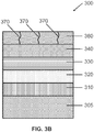
- top contact layer 350 and/or cap layer 360 may relax without introducing deleterious defects into the active layers below which would adversely affect the performance of PUVLED structure 300 (as described below with reference to Figure 3B ).
- Each of layers 310 - 350 is pseudomorphic, and each layer individually may have a thickness greater than its predicted critical thickness.
- the collective layer structure including layers 310 - 350 may have a total thickness greater than the predicted critical thickness for the layers considered collectively (i.e., for a multiple-layer structure, the entire structure has a predicted critical thickness even when each individual layer would be less than a predicted critical thickness thereof considered in isolation).
- layers 310 - 340 of PUVLED structure 300 are pseudomorphic, and cap layer 360 is intentionally relaxed. As shown in Figure 3B , layers 310 - 340 are formed as described above with reference to Figure 3A . Cap layer 360 is subsequently formed in a partially or substantially strain-relaxed state via judicious selection of its composition and/or the deposition conditions. For example, the lattice mismatch between cap layer 360 and substrate 305 and/or MQW layer 330 may be greater than approximately 1%, greater than approximately 2%, or even greater than approximately 3%.
- cap layer 360 includes or consists essentially of undoped or doped GaN
- substrate 305 includes or consists essentially of AIN
- MQW layer 330 includes or consists essentially of multiple Al 0.55 Ga 0.45 N quantum wells interleaved with Al 0.75 Ga 0.25 N barrier layers
- cap layer 360 is lattice mismatched by approximately 2.4%.
- Cap layer 360 may be substantially relaxed, i.e., may have a lattice parameter approximately equal to its theoretical unstrained lattice constant.
- a partially or substantially relaxed cap layer 360 may contain strain-relieving dislocations 370 having segments threading to the surface of cap layer 360 (such dislocations may be termed "threading dislocations").
- the threading dislocation density of a relaxed cap layer 360 may be larger than that of substrate 305 and/or layers 310-340 by, e.g., one, two, or three orders of magnitude, or even larger.
- Cap layer 360 is preferably not formed as a series of coalesced or uncoalesced islands, as such islanding may deleteriously impact the surface roughness of cap layer 360.
- an undoped graded layer is formed between layers 310 - 340 and cap layer 360, and its composition at its interfaces with layers 340, 360 substantially matches the compositions of those layers.
- the thickness of this graded layer which is preferably pseudomorphically strained, may range between approximately 10 nm and approximately 50 nm, e.g., approximately 30 nm.
- epitaxial growth may be temporarily stopped between growth of the graded layer and cap layer 360.
- an electron-blocking layer 340 including or consisting essentially of Al 0.8 Ga 0.2 N or Al 0.85 Ga 0.15 N is formed over MQW layer 330.
- a graded layer is formed over electron-blocking layer 340 prior to formation of cap layer 360 including or consisting essentially of GaN.
- the graded layer may be graded in composition from, for example, Al 0.85 Ga 0.15 N to GaN over a thickness of approximately 30 nm.
- the graded layer may be formed by, e.g., MOCVD, and in this embodiment is formed by ramping the flow of TMA and TMG (by ramping the flow of hydrogen through their respective bubblers) from the conditions utilized to form electron-blocking layer 340 to 0 standard cubic centimeters per minute (sccm) and 6.4 sccm, respectively, over a period of approximately 24 minutes, thus resulting in a monotonic grade from Al 0.85 Ga 0.15 N to GaN (all of the other growth conditions are substantially fixed).
- the thickness of the graded layer in this exemplary embodiment is approximately 30 nm, and a hole concentration of approximately 3 ⁇ 10 19 cm -3 may be achieved through polarization doping without impurity doping (i.e., being free of doping impurities), as modeled using SiLENSe software.
- polarization doping is enabled by the polarization in nitride materials that is due to the difference in electronegativity between the metal atoms and the nitrogen atoms. This results in a polarization field along asymmetric directions in the wurtzite crystal structure.
- strain in the layers may result in additional piezoelectric polarization fields and thus additional polarization doping.
- graded composition layers e.g., three-dimensional volumes
- the magnitude of the total charge is defined by the difference in Al compositions within the graded layer, i.e., the difference between the starting composition and the final composition.
- the concentration of carriers is defined by the total charge divided by the graded layer thickness. A very high carrier concentration may be achieved by a high composition change over a small thickness, while a lower composition change or larger grading thickness typically results in a smaller carrier concentration; however, for a given composition change the total number of carriers is generally constant.
- illustrative examples from the present disclosure utilize very thin SPG layers in order to minimize absorption of UV photons therein.
- SPG layers preferably have thicknesses of less than 50 nm, e.g., between approximately 10 nm and approximately 30 nm.
- smooth (25-50 nm) p-GaN layers were grown on a typical pseudomorphic LED structure (AlN/n-AlGaN/MQW/electron-blocking layer/p-GaN) by MOCVD and trimethylgallium (TMGa) and NH 3 were used as Ga and N precursors.
- TMGa trimethylgallium
- Some conventional p-GaN layers are grown at 1000°C and at a pressure of 100 Torr, and often these layers are rough, exhibiting an islanded or pyramidal morphology. Such approaches are encouraged by the conventional wisdom in the art, which indicates that one should enhance the mobility of the Ga adatom to promote lateral growth and coalescence of the layer. Thus, conventional wisdom teaches that contact-layer growth should use increased V/III ratios and higher temperatures. However, such techniques were unable to achieve smooth surfaces on the pseudomorphic layer in the thickness range utilized in embodiments of the present invention. Notably, the large strain in the pseudomorphic layer enhances island formation and increased surface roughness.
- growth temperatures of 850 °C - 900 °C may be utilized for growth of the SPG (cap) layer, and growth pressures of 20 Torr may be utilized to enhance the adatom mobility at this lower growth-temperature regime.
- the growth rate of smooth p-GaN is only approximately 5 nm/min.
- the morphological and elemental properties of resulting SPG layers were investigated using atomic force microscopy (AFM) and secondary ion mass spectroscopy (SIMS).
- AFM shows smoother p-GaN layers (Rq value of approximately 0.85 nm) as shown in Figure 4A , compared to the rougher morphology of conventional p-GaN (Rq value of approximately 7.2 nm) shown in Figure 4B .
- the actual island heights are over 50 nm and these thicker islands result in higher absorption and also leave areas uncovered by p-GaN which will result in poor p-contact by the contact metallization when these holes occur in the regions that are covered by the contact metallization.
- SIMS analysis shows higher doping concentration (by a factor of two) in the smooth p-GaN compared to the conventional p-GaN; however, the concentration is not constant and does not reach equilibrium until growth of ⁇ 25 nm of p-GaN, resulting in difficulties making ohmic contacts to layers thinner than 25 nm.
- a soak i.e., exposure within the deposition chamber, (of, e.g., 1-10 minutes, for example 5 minutes) with only the dopant (e.g., Mg) source (i.e., no Ga source) flowing may be utilized to saturate the surface prior to growth initiation.
- Cp2Mg bis-cyclopentadienylmagnesium
- the precursor may be disposed within a bubbler, and a carrier gas such as nitrogen or hydrogen may be flowed into the bubbler to form a gas solution saturated with the dopant precursor.
- a carrier gas such as nitrogen or hydrogen
- This enables higher dopant concentration and good ohmic contact formation to layers as thin as 5 nm.
- very thin p-GaN layers ( ⁇ 10 nm) may be easily realized in this growth regime owing to the slower growth rate and the conformal morphology while the doping concentrations may be optimized by adjusting the input precursor flows.
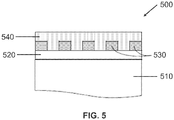
- polarization doping and a thin SPG layer are combined with a patterned reflector as shown in Figure 5 , which depicts a portion of a UV LED device 500.
- region 510 includes or consists essentially of the AlN substrate and the active region of the device, for example as detailed above and illustrated in Figure 3A .
- Region 510 is topped with a SPG layer 520, which is kept smooth to enable a very thin layer with high UV transparency.
- a contact layer 530, formed on the SPG layer 520, is typically substantially not UV reflective but forms a good ohmic contact to the SPG layer 520.
- contact layer 530 includes or consists essentially of Ni/Au.
- the contact layer is, in preferred embodiments, patterned onto the surface of SPG layer 520.
- the spacing between individual portions of contact layer 530 may be defined via, e.g., conventional photolithography.
- the pattern may be in the form of lines or patterns of isolated "pixels" (or “islands") as shown in Figure 5 .
- Lines may have widths of, for example, 1 ⁇ m to 50 ⁇ m, e.g., 5 ⁇ m, and may have spacings therebetween of, for example 1 ⁇ m to 50 ⁇ m, e.g., 5 ⁇ m.
- Pixels may be, for example, substantially cubic or rectangular solids or may even be substantially hemispherical, and pixels may have a dimension such as width, length, or diameter of, for example, 1 ⁇ m to 50 ⁇ m, e.g., 5 ⁇ m.
- the contact area and the spacing are typically defined to optimize the wall plug efficiency of the device.
- the contact layer 530 may be capped with a reflector 540 formed both above the contact layer 530 (or isolated portions thereof) and between portions of the contact layer 530 (i.e., in direct contact with SPG layer 520).
- the reflector 540 typically includes or consists essentially of a metal (or metal alloy) that is highly reflective to UV light but that does not form a good ohmic contact to the SPG layer 520.
- the reflector 540 may include or consist essentially of Al.
- the contact area of the contact layer 530 will generally determine, at least in part, the effective contact resistance of the combined contact layer 530 and reflector 540.
- the contact layer 530 For instance, if 10% of the area is covered by the contact layer 530, then the effective contact resistance is increased by a factor of ten. However, at the same time, the reflector area (i.e., the area of SPG layer 520 capped directly by reflector 540, without contact layer 530 therebetween) is increased. In an exemplary embodiment, the contact resistivity of the contact layer 530 is less than approximately 1.0 m ⁇ -cm 2 , or even less than approximately 0.5 m ⁇ -cm 2 .
- the effective contact resistance is increased to 5 m ⁇ and the effective (averaged over all area) reflector is reduced by 10% (e.g., a 90% reflectivity of the reflector 540 is effectively reduced to 81%).
- the size of individual metal contact pixels of contact layer 530 is preferably kept as small as possible so that current spreading from the individual contact pixels occurs. This increases the probability that the generated photons will strike the reflector 540 rather than the contact pixel of contact layer 530 (which would typically occur if the current traveled straight down from the contact metal pixel of contact layer 530).
- the polarization-doped AlGaN enables current spreading while maintaining transparency even with a thin SPG layer 520; the thin SPG layer 520 is used primarily to lower the contact resistance while maintaining low absorption. This is in direct contrast to conventional methods where p-doping in high Al content Al x Ga 1-x N is highly resistive and will not allow current spreading.
- Embodiments of the invention may utilize photon-extraction techniques described in the '093 application.
- Such techniques include surface treatment (e.g., roughening, texturing, and/or patterning), substrate thinning, substrate removal, and/or the use of rigid lenses with thin intermediate encapsulant layers.
- Exemplary substrate-removal techniques include laser lift-off, as described in " High brightness LEDs for general lighting applications using the new Thin GaNTM - Technology", V. Haerle, et al., Phys. Stat. Sol. (a) 201, 2736 (2004 ).
- the back surface of the substrate may be ground, for example, with a 600 to 1800 grit wheel.
- the removal rate of this step may be purposefully maintained at a low level (approximately 0.3 - 0.4 ⁇ m/s) in order to avoid damaging the substrate or the device layers thereover.
- the back surface may be polished with a polishing slurry, e.g., a solution of equal parts of distilled water and a commercial colloidal suspension of silica in a buffered solution of KOH and water.
- the removal rate of this step may vary between approximately 10 ⁇ m/min and approximately 15 ⁇ m/min.
- the substrate may be thinned down to a thickness of approximately 200 ⁇ m to approximately 250 ⁇ m, or even to a thickness of approximately 20 ⁇ m to approximately 50 ⁇ m, although the present disclosure is not limited by this range. In other embodiments, the substrate is thinned to approximately 20 ⁇ m or less, or even substantially completely removed.
- the thinning step is preferably followed by wafer cleaning in, e.g., one or more organic solvents. In one embodiment of the invention, the cleaning step includes immersion of the substrate in boiling acetone for approximately 10 minutes, followed by immersion in boiling methanol for approximately 10 minutes.
Landscapes
- Led Devices (AREA)
- Electrodes Of Semiconductors (AREA)
Claims (15)
- Procédé de formation d'un contact à un dispositif électroluminescent ultraviolet (UV) (300, 500), le procédé comprenant :la mise à disposition d'un substrat (305) ayant une surface supérieure d'AlyGa1-yN, avec y ≥ 0,4 ;la formation d'une structure de dispositif électroluminescent actif (330) sur le substrat, la structure de dispositif comprenant une pluralité de couches comprenant chacune AlxGa1-xN ;la formation d'une couche d'Al1-zGazN graduée non dopée sur la structure de dispositif, une composition de la couche graduée étant graduée en concentration de Ga z de telle sorte que la concentration de Ga z augmente dans une direction s'éloignant de la structure de dispositif électroluminescent ;la formation sur la couche graduée d'une couche de coiffage d'Al1-wGawN à dopage p (360) ayant (i) une épaisseur comprise entre 2 nm et 30 nm, (ii) une rugosité de surface de moins de 6 nm sur une taille d'échantillon de 200 µm x 300 µm, et (iii) une concentration de Ga w ≥ 0,8 ; etla formation sur la couche de coiffage d'Al1-wGawN d'un contact métallique (530) comprenant au moins un métal, le contact métallique ayant une résistivité de contact à la couche de coiffage d'Al1-wGawN de moins de 1,0 mΩ-cm2.
- Procédé de la revendication 1, dans lequel la formation de la couche de coiffage d'Al1-wGawN comprend une croissance épitaxiale à une température comprise entre 850 °C et 900 °C et une pression de croissance de moins de 50 Torr.
- Procédé de la revendication 2, dans lequel la pression de croissance est de 20 Torr.
- Procédé de l'une quelconque des revendications précédentes, dans lequel la formation de la couche de coiffage d'Al1-wGawN comprend une croissance épitaxiale à un taux de croissance compris entre 0,5 nm/min et 5 nm/min.
- Procédé de l'une quelconque des revendications précédentes, comprenant en outre, entre la formation de la couche graduée et la formation de la couche de coiffage d'Al1-wGawN, l'exposition d'une surface de la couche graduée à un précurseur du dopant de type p de la couche de coiffage sans exposition à un précurseur de Ga, éventuellement dans lequel le dopant de type p de la couche de coiffage comprend du Mg.
- Dispositif électroluminescent ultraviolet (UV) (300, 500) comprenant :un substrat (305) ayant une surface supérieure d'AlyGa1-yN, avec y ≥ 0,4 ;une structure de dispositif électroluminescent actif (330) disposée sur le substrat, la structure de dispositif comprenant une pluralité de couches comprenant chacune AlxGa1-xN ;une couche d'Al1-zGazN graduée non dopée disposée sur la structure de dispositif, une composition de la couche graduée étant graduée en concentration de Ga z de telle sorte que la concentration de Ga z augmente dans une direction s'éloignant de la structure de dispositif électroluminescent ;une couche de coiffage d'Al1-wGawN à dopage p (360) disposée sur la couche graduée, la couche de coiffage d'Al1-wGawN à dopage p ayant (i) une épaisseur comprise entre 2 nm et 30 nm, (ii) une rugosité de surface de moins de 6 nm sur une taille d'échantillon de 200 µm x 300 µm, et (iii) une concentration de Ga w ≥ 0,8 ; etun contact métallique (530) disposé sur la couche de coiffage d'Al1-wGawN et comprenant au moins un métal, le contact métallique ayant une résistivité de contact à la couche de coiffage d'Al1-wGawN de moins de 1,0 mΩ-cm2.
- Procédé de l'une quelconque des revendications 1 à 5 ou dispositif électroluminescent de la revendication 6, dans lequel la couche de coiffage d'Al1-wGawN est dopée avec du Mg et/ou la couche de coiffage d'Al1-wGawN est au moins partiellement relaxée.
- Procédé de l'une quelconque des revendications 1 à 5 ou dispositif électroluminescent de la revendication 6 ou la revendication 7, dans lequel le dispositif électroluminescent a les caractéristiques (A) et/ou (B) :(A) le dispositif électroluminescent a une efficacité d'extraction de photons de plus de 25 %, et/ou(B) la couche graduée et la couche de coiffage d'Al1-wGawN absorbent collectivement moins de 80 % des photons UV générés par la structure de dispositif électroluminescent et ayant une longueur d'onde de moins de 340 nm.
- Procédé de l'une quelconque des revendications 1 à 5 ou dispositif électroluminescent de l'une quelconque des revendications 6 à 8, dans lequel ledit au moins un métal du contact métallique comprend Ni/Au ou Pd.
- Procédé de l'une quelconque des revendications 1 à 5 ou dispositif électroluminescent de l'une quelconque des revendications 6 à 9, dans lequel le contact métallique a une réflectivité à la lumière générée par la structure de dispositif électroluminescent de 60 % ou moins, éventuellement de 30 % ou moins.
- Procédé de l'une quelconque des revendications 1 à 5 ou dispositif électroluminescent de l'une quelconque des revendications 6 à 10, dans lequel le contact métallique a la forme d'une pluralité de lignes discrètes et/ou de pixels dudit au moins un métal, des portions de la couche de coiffage d'Al1-wGawN n'étant pas couvertes par le contact métallique.
- Procédé ou dispositif électroluminescent de la revendication 11, comprenant en outre un réflecteur (540) disposé sur le contact métallique et les portions non couvertes de la couche de coiffage d'Al1-wGawN, éventuellement dans lequel le réflecteur :comprend un métal ayant plus de 90 % de réflectivité à la lumière UV et une fonction de travail de moins de 4,5 eV ; et/oua une résistivité de contact à la couche de coiffage d'Al1-wGawN de plus de 5 mΩ-cm2; éventuellement de plus de 10 mΩ-cm2 ; et/oucomprend de l'Al.
- Procédé de l'une quelconque des revendications 1 à 5 ou dispositif électroluminescent de l'une quelconque des revendications 7 à 12, dans lequel le dispositif électroluminescent comprend une diode électroluminescente.
- Procédé de l'une quelconque des revendications 1 à 5 ou dispositif électroluminescent de l'une quelconque des revendications 7 à 13, dans lequel (i) une portion de fond de la couche graduée proche de la structure de dispositif actif a une concentration de Ga z égale à une concentration de Ga d'une couche (340) directement en dessous et (ii) une portion supérieure de la couche graduée opposée à la portion de fond de la couche graduée a une concentration de Ga z de 1.
- Procédé de l'une quelconque des revendications 1 à 5 ou dispositif électroluminescent de l'une quelconque des revendications 7 à 14, dans lequel le substrat consiste en de l'AIN dopé ou non dopé.
Applications Claiming Priority (2)
| Application Number | Priority Date | Filing Date | Title |
|---|---|---|---|
| US201361788141P | 2013-03-15 | 2013-03-15 | |
| PCT/US2014/025317 WO2014151264A1 (fr) | 2013-03-15 | 2014-03-13 | Contacts planaires pour des dispositifs électroniques et optoélectroniques pseudomorphes |
Publications (3)
| Publication Number | Publication Date |
|---|---|
| EP2973664A1 EP2973664A1 (fr) | 2016-01-20 |
| EP2973664A4 EP2973664A4 (fr) | 2016-08-10 |
| EP2973664B1 true EP2973664B1 (fr) | 2020-10-14 |
Family
ID=51523549
Family Applications (1)
| Application Number | Title | Priority Date | Filing Date |
|---|---|---|---|
| EP14769060.6A Active EP2973664B1 (fr) | 2013-03-15 | 2014-03-13 | Dispositif émetteur d'ultraviolet et procédé pour former un contact sur un dispositif émetteur d'ultraviolet |
Country Status (5)
| Country | Link |
|---|---|
| US (4) | US20150280057A1 (fr) |
| EP (1) | EP2973664B1 (fr) |
| JP (2) | JP6275817B2 (fr) |
| CN (2) | CN108511567A (fr) |
| WO (1) | WO2014151264A1 (fr) |
Families Citing this family (31)
| Publication number | Priority date | Publication date | Assignee | Title |
|---|---|---|---|---|
| US8545629B2 (en) | 2001-12-24 | 2013-10-01 | Crystal Is, Inc. | Method and apparatus for producing large, single-crystals of aluminum nitride |
| US7641735B2 (en) | 2005-12-02 | 2010-01-05 | Crystal Is, Inc. | Doped aluminum nitride crystals and methods of making them |
| US9034103B2 (en) | 2006-03-30 | 2015-05-19 | Crystal Is, Inc. | Aluminum nitride bulk crystals having high transparency to ultraviolet light and methods of forming them |
| US9771666B2 (en) | 2007-01-17 | 2017-09-26 | Crystal Is, Inc. | Defect reduction in seeded aluminum nitride crystal growth |
| WO2008088838A1 (fr) | 2007-01-17 | 2008-07-24 | Crystal Is, Inc. | Réduction des défauts de croissance de cristaux de nitrure d'aluminium ensemencés |
| US8080833B2 (en) | 2007-01-26 | 2011-12-20 | Crystal Is, Inc. | Thick pseudomorphic nitride epitaxial layers |
| JP5806734B2 (ja) | 2010-06-30 | 2015-11-10 | クリスタル アイエス, インコーポレーテッドCrystal Is, Inc. | 熱勾配制御による窒化アルミニウム大単結晶成長 |
| US8962359B2 (en) | 2011-07-19 | 2015-02-24 | Crystal Is, Inc. | Photon extraction from nitride ultraviolet light-emitting devices |
| EP2973664B1 (fr) * | 2013-03-15 | 2020-10-14 | Crystal Is, Inc. | Dispositif émetteur d'ultraviolet et procédé pour former un contact sur un dispositif émetteur d'ultraviolet |
| US9412911B2 (en) | 2013-07-09 | 2016-08-09 | The Silanna Group Pty Ltd | Optical tuning of light emitting semiconductor junctions |
| WO2015157178A1 (fr) | 2014-04-07 | 2015-10-15 | Crystal Is, Inc. | Dispositif émetteur de lumière ultraviolette et procédés |
| WO2015181656A1 (fr) | 2014-05-27 | 2015-12-03 | The Silanna Group Pty Limited | Dispositifs électroniques comprenant des super-réseaux de type n et de type p |
| US11322643B2 (en) | 2014-05-27 | 2022-05-03 | Silanna UV Technologies Pte Ltd | Optoelectronic device |
| KR102318317B1 (ko) | 2014-05-27 | 2021-10-28 | 실라나 유브이 테크놀로지스 피티이 리미티드 | 반도체 구조물과 초격자를 사용하는 진보된 전자 디바이스 구조 |
| WO2015181648A1 (fr) | 2014-05-27 | 2015-12-03 | The Silanna Group Pty Limited | Dispositif optoélectronique |
| US9673287B2 (en) * | 2014-12-15 | 2017-06-06 | Infineon Technologies Americas Corp. | Reliable and robust electrical contact |
| US9680057B2 (en) * | 2015-09-17 | 2017-06-13 | Crystal Is, Inc. | Ultraviolet light-emitting devices incorporating two-dimensional hole gases |
| WO2017145026A1 (fr) | 2016-02-23 | 2017-08-31 | Silanna UV Technologies Pte Ltd | Dispositif électroluminescent à cavité optique résonante |
| US10418517B2 (en) | 2016-02-23 | 2019-09-17 | Silanna UV Technologies Pte Ltd | Resonant optical cavity light emitting device |
| CN105720144B (zh) * | 2016-03-24 | 2021-09-24 | 晶能光电(江西)有限公司 | 一种硅衬底氮化物紫外led芯片结构及其实现方法 |
| AT519500B1 (de) * | 2017-01-03 | 2019-03-15 | Univ Linz | Lichtemittierendes Halbleiterelement |
| WO2018232080A1 (fr) * | 2017-06-16 | 2018-12-20 | Crystal Is. Inc. | Croissance par ensemencement en deux étapes de monocristaux de nitrure d'aluminium de grande taille |
| CN111630630A (zh) | 2017-11-10 | 2020-09-04 | 晶化成半导体公司 | 大尺寸紫外透明氮化铝单晶及其制备方法 |
| CN112567079B (zh) | 2018-06-19 | 2023-12-26 | 晶化成半导体公司 | 深紫外透明的氮化铝晶体及其形成方法 |
| US10622514B1 (en) | 2018-10-15 | 2020-04-14 | Silanna UV Technologies Pte Ltd | Resonant optical cavity light emitting device |
| EP3873853B1 (fr) | 2018-11-02 | 2025-09-17 | Crystal IS, Inc. | Systèmes et procédés pour la désinfection de fluides par lumière ultraviolette |
| US11312905B2 (en) * | 2019-07-11 | 2022-04-26 | Nanosys, Inc. | Blue-emitting nanocrystals with cubic shape and fluoride passivation |
| WO2021072616A1 (fr) * | 2019-10-15 | 2021-04-22 | 厦门三安光电有限公司 | Diode électroluminescente |
| CN111554784B (zh) * | 2020-07-09 | 2020-09-25 | 华灿光电(浙江)有限公司 | 发光二极管外延片及其生长方法 |
| US11990562B1 (en) * | 2020-10-07 | 2024-05-21 | Crystal Is, Inc. | Ultraviolet light-emitting devices having enhanced light output |
| CN114765344B (zh) * | 2021-01-15 | 2025-07-11 | 山东华光光电子股份有限公司 | 一种优化电子阻挡层的小功率AlGaInP红光半导体激光器及其制备方法 |
Family Cites Families (263)
| Publication number | Priority date | Publication date | Assignee | Title |
|---|---|---|---|---|
| NL6615059A (fr) | 1966-10-25 | 1968-04-26 | ||
| US3600701A (en) | 1968-03-14 | 1971-08-17 | Gen Electric | Signal generator for producing a set of signals at baseband frequency and with adjustable phase slope |
| US3531245A (en) | 1968-04-01 | 1970-09-29 | Du Pont | Magnesium-aluminum nitrides |
| US3607014A (en) | 1968-12-09 | 1971-09-21 | Dow Chemical Co | Method for preparing aluminum nitride and metal fluoride single crystals |
| US3603414A (en) | 1970-01-30 | 1971-09-07 | Frank E Stebley | Insert for drilling unit |
| US3768983A (en) | 1971-11-03 | 1973-10-30 | North American Rockwell | Single crystal beryllium oxide growth from calcium oxide-beryllium oxide melts |
| US3903357A (en) | 1971-12-06 | 1975-09-02 | Westinghouse Electric Corp | Adaptive gate video gray level measurement and tracker |
| FR2225207B1 (fr) | 1973-04-16 | 1978-04-21 | Ibm | |
| US3933573A (en) | 1973-11-27 | 1976-01-20 | The United States Of America As Represented By The Secretary Of The Air Force | Aluminum nitride single crystal growth from a molten mixture with calcium nitride |
| US4008851A (en) | 1976-01-16 | 1977-02-22 | Curt G. Joa, Inc. | Adhesive tape bag closure |
| DE2750607A1 (de) | 1977-11-11 | 1979-05-17 | Max Planck Gesellschaft | Luftbestaendiges kristallines lithiumnitrid, verfahren zu seiner herstellung und seine verwendung |
| US4547471A (en) | 1983-11-18 | 1985-10-15 | General Electric Company | High thermal conductivity aluminum nitride ceramic body |
| JPS61236686A (ja) | 1985-04-13 | 1986-10-21 | Tohoku Metal Ind Ltd | 単結晶育成法 |
| JP2745408B2 (ja) | 1988-07-07 | 1998-04-28 | 東芝セラミックス株式会社 | 半導体単結晶引上げ装置 |
| US5258218A (en) | 1988-09-13 | 1993-11-02 | Kabushiki Kaisha Toshiba | Aluminum nitride substrate and method for producing same |
| US5057287A (en) | 1988-11-01 | 1991-10-15 | Sfa, Inc. | Liquid encapsulated zone melting crystal growth method and apparatus |
| JPH02263445A (ja) | 1988-12-23 | 1990-10-26 | Toshiba Corp | 窒化アルミニウム基板およびそれを用いた半導体装置 |
| US5087949A (en) | 1989-06-27 | 1992-02-11 | Hewlett-Packard Company | Light-emitting diode with diagonal faces |
| JPH03285075A (ja) | 1990-03-30 | 1991-12-16 | Nisshin Steel Co Ltd | タングステンルツボの製造方法 |
| EP0509312B1 (fr) | 1991-04-16 | 1995-08-23 | Sumitomo Electric Industries, Limited | Procédé Czochralski utilisant un élément pour intercepter la radiation de la solution fondue due matériau brut et appareil à ce but |
| EP0544329A3 (en) | 1991-11-28 | 1993-09-01 | Kabushiki Kaisha Toshiba | Semiconductor package |
| US5578839A (en) | 1992-11-20 | 1996-11-26 | Nichia Chemical Industries, Ltd. | Light-emitting gallium nitride-based compound semiconductor device |
| US5777364A (en) * | 1992-11-30 | 1998-07-07 | International Business Machines Corporation | Graded channel field effect transistor |
| JP2875726B2 (ja) | 1993-10-28 | 1999-03-31 | 新日本無線株式会社 | 化合物半導体の熱処理方法 |
| US6083812A (en) | 1993-02-02 | 2000-07-04 | Texas Instruments Incorporated | Heteroepitaxy by large surface steps |
| DE69425186T3 (de) * | 1993-04-28 | 2005-04-14 | Nichia Corp., Anan | Halbleitervorrichtung aus einer galliumnitridartigen III-V-Halbleiterverbindung und Verfahren zu ihrer Herstellung |
| US5520785A (en) | 1994-01-04 | 1996-05-28 | Motorola, Inc. | Method for enhancing aluminum nitride |
| DE69526748T2 (de) | 1994-02-25 | 2002-09-05 | Sumitomo Electric Industries, Ltd. | Substrat für aluminium-nitrid dünne Film und Verfahren zu seiner Herstellung |
| US5525320A (en) | 1994-07-11 | 1996-06-11 | University Of Cincinnati | Process for aluminum nitride powder production |
| JPH0859386A (ja) | 1994-08-22 | 1996-03-05 | Mitsubishi Materials Corp | 半導体単結晶育成装置 |
| US5679965A (en) * | 1995-03-29 | 1997-10-21 | North Carolina State University | Integrated heterostructures of Group III-V nitride semiconductor materials including epitaxial ohmic contact, non-nitride buffer layer and methods of fabricating same |
| US5670798A (en) | 1995-03-29 | 1997-09-23 | North Carolina State University | Integrated heterostructures of Group III-V nitride semiconductor materials including epitaxial ohmic contact non-nitride buffer layer and methods of fabricating same |
| EP0992470B1 (fr) | 1995-08-03 | 2006-03-08 | Ngk Insulators, Ltd. | Corps frittés en nitrure d'aluminium et leur utilisation comme substrat dans un dispositif pour la fabrication de semiconducteurs |
| JP3604205B2 (ja) | 1995-09-18 | 2004-12-22 | 日亜化学工業株式会社 | 窒化物半導体の成長方法 |
| US5981980A (en) | 1996-04-22 | 1999-11-09 | Sony Corporation | Semiconductor laminating structure |
| JP3876473B2 (ja) | 1996-06-04 | 2007-01-31 | 住友電気工業株式会社 | 窒化物単結晶及びその製造方法 |
| JP3644191B2 (ja) | 1996-06-25 | 2005-04-27 | 住友電気工業株式会社 | 半導体素子 |
| US5858086A (en) | 1996-10-17 | 1999-01-12 | Hunter; Charles Eric | Growth of bulk single crystals of aluminum nitride |
| US5954874A (en) | 1996-10-17 | 1999-09-21 | Hunter; Charles Eric | Growth of bulk single crystals of aluminum nitride from a melt |
| US6533874B1 (en) | 1996-12-03 | 2003-03-18 | Advanced Technology Materials, Inc. | GaN-based devices using thick (Ga, Al, In)N base layers |
| US5868837A (en) | 1997-01-17 | 1999-02-09 | Cornell Research Foundation, Inc. | Low temperature method of preparing GaN single crystals |
| JP3239787B2 (ja) | 1997-01-30 | 2001-12-17 | 安藤電気株式会社 | Icソケット |
| US6583444B2 (en) | 1997-02-18 | 2003-06-24 | Tessera, Inc. | Semiconductor packages having light-sensitive chips |
| JPH10335637A (ja) * | 1997-05-30 | 1998-12-18 | Sony Corp | ヘテロ接合電界効果トランジスタ |
| US6229160B1 (en) | 1997-06-03 | 2001-05-08 | Lumileds Lighting, U.S., Llc | Light extraction from a semiconductor light-emitting device via chip shaping |
| US6270569B1 (en) | 1997-06-11 | 2001-08-07 | Hitachi Cable Ltd. | Method of fabricating nitride crystal, mixture, liquid phase growth method, nitride crystal, nitride crystal powders, and vapor phase growth method |
| JP3776565B2 (ja) | 1997-06-12 | 2006-05-17 | 株式会社コトブキ | 伸縮式階段状観覧席 |
| US6006620A (en) | 1997-12-01 | 1999-12-28 | Chrysler Corporation | Automated manual transmission controller |
| EP0979883A4 (fr) | 1997-12-25 | 2003-10-15 | Japan Energy Corp | Procede de preparation de monocristaux de composes semi-conducteurs, equipement pour ce procede et monocristaux de composes semi-conducteurs |
| US6091085A (en) | 1998-02-19 | 2000-07-18 | Agilent Technologies, Inc. | GaN LEDs with improved output coupling efficiency |
| JP4214585B2 (ja) | 1998-04-24 | 2009-01-28 | 富士ゼロックス株式会社 | 半導体デバイス、半導体デバイスの製造方法及び製造装置 |
| JP4166885B2 (ja) * | 1998-05-18 | 2008-10-15 | 富士通株式会社 | 光半導体装置およびその製造方法 |
| US6218207B1 (en) | 1998-05-29 | 2001-04-17 | Mitsushita Electronics Corporation | Method for growing nitride semiconductor crystals, nitride semiconductor device, and method for fabricating the same |
| JP3439994B2 (ja) | 1998-07-07 | 2003-08-25 | 科学技術振興事業団 | 低抵抗n型および低抵抗p型単結晶AlN薄膜の合成法 |
| US6045612A (en) | 1998-07-07 | 2000-04-04 | Cree, Inc. | Growth of bulk single crystals of aluminum nitride |
| KR100277968B1 (ko) | 1998-09-23 | 2001-03-02 | 구자홍 | 질화갈륨 기판 제조방법 |
| US6063185A (en) | 1998-10-09 | 2000-05-16 | Cree, Inc. | Production of bulk single crystals of aluminum nitride, silicon carbide and aluminum nitride: silicon carbide alloy |
| US6086672A (en) | 1998-10-09 | 2000-07-11 | Cree, Inc. | Growth of bulk single crystals of aluminum nitride: silicon carbide alloys |
| US6048813A (en) | 1998-10-09 | 2000-04-11 | Cree, Inc. | Simulated diamond gemstones formed of aluminum nitride and aluminum nitride: silicon carbide alloys |
| US6404125B1 (en) | 1998-10-21 | 2002-06-11 | Sarnoff Corporation | Method and apparatus for performing wavelength-conversion using phosphors with light emitting diodes |
| US6218293B1 (en) | 1998-11-13 | 2001-04-17 | Micron Technology, Inc. | Batch processing for semiconductor wafers to form aluminum nitride and titanium aluminum nitride |
| JP3015887B1 (ja) | 1998-11-19 | 2000-03-06 | 科学技術庁金属材料技術研究所長 | バルク単結晶育成方法 |
| US6187089B1 (en) | 1999-02-05 | 2001-02-13 | Memc Electronic Materials, Inc. | Tungsten doped crucible and method for preparing same |
| US6838705B1 (en) * | 1999-03-29 | 2005-01-04 | Nichia Corporation | Nitride semiconductor device |
| US6592663B1 (en) | 1999-06-09 | 2003-07-15 | Ricoh Company Ltd. | Production of a GaN bulk crystal substrate and a semiconductor device formed on a GaN bulk crystal substrate |
| US6829273B2 (en) | 1999-07-16 | 2004-12-07 | Agilent Technologies, Inc. | Nitride semiconductor layer structure and a nitride semiconductor laser incorporating a portion of same |
| RU2158789C1 (ru) | 1999-08-04 | 2000-11-10 | Водаков Юрий Александрович | Способ эпитаксиального выращивания монокристаллического нитрида алюминия и ростовая камера для осуществления способа |
| JP4145437B2 (ja) | 1999-09-28 | 2008-09-03 | 住友電気工業株式会社 | 単結晶GaNの結晶成長方法及び単結晶GaN基板の製造方法と単結晶GaN基板 |
| US6398867B1 (en) | 1999-10-06 | 2002-06-04 | General Electric Company | Crystalline gallium nitride and method for forming crystalline gallium nitride |
| US6350393B2 (en) | 1999-11-04 | 2002-02-26 | Cabot Microelectronics Corporation | Use of CsOH in a dielectric CMP slurry |
| JP2001192647A (ja) | 2000-01-14 | 2001-07-17 | Seimi Chem Co Ltd | 酸化セリウム含有研磨用組成物及び研磨方法 |
| US6879615B2 (en) | 2000-01-19 | 2005-04-12 | Joseph Reid Henrichs | FCSEL that frequency doubles its output emissions using sum-frequency generation |
| US6698647B1 (en) | 2000-03-10 | 2004-03-02 | Honeywell International Inc. | Aluminum-comprising target/backing plate structures |
| US6596079B1 (en) | 2000-03-13 | 2003-07-22 | Advanced Technology Materials, Inc. | III-V nitride substrate boule and method of making and using the same |
| US6447604B1 (en) | 2000-03-13 | 2002-09-10 | Advanced Technology Materials, Inc. | Method for achieving improved epitaxy quality (surface texture and defect density) on free-standing (aluminum, indium, gallium) nitride ((al,in,ga)n) substrates for opto-electronic and electronic devices |
| US6627974B2 (en) | 2000-06-19 | 2003-09-30 | Nichia Corporation | Nitride semiconductor substrate and method for manufacturing the same, and nitride semiconductor device using nitride semiconductor substrate |
| US7064355B2 (en) | 2000-09-12 | 2006-06-20 | Lumileds Lighting U.S., Llc | Light emitting diodes with improved light extraction efficiency |
| JP2002141556A (ja) | 2000-09-12 | 2002-05-17 | Lumileds Lighting Us Llc | 改良された光抽出効果を有する発光ダイオード |
| US6777717B1 (en) | 2000-09-21 | 2004-08-17 | Gelcore, Llc | LED reflector for improved light extraction |
| US7053413B2 (en) | 2000-10-23 | 2006-05-30 | General Electric Company | Homoepitaxial gallium-nitride-based light emitting device and method for producing |
| JP2002222771A (ja) | 2000-11-21 | 2002-08-09 | Ngk Insulators Ltd | Iii族窒化物膜の製造方法、iii族窒化物膜の製造用下地膜、及びその下地膜の製造方法 |
| US6548333B2 (en) | 2000-12-01 | 2003-04-15 | Cree, Inc. | Aluminum gallium nitride/gallium nitride high electron mobility transistors having a gate contact on a gallium nitride based cap segment |
| JP2005167275A (ja) | 2000-12-07 | 2005-06-23 | Ngk Insulators Ltd | 半導体素子 |
| US6649287B2 (en) * | 2000-12-14 | 2003-11-18 | Nitronex Corporation | Gallium nitride materials and methods |
| JP2002274996A (ja) | 2001-01-15 | 2002-09-25 | Ngk Insulators Ltd | エピタキシャル下地基板及びエピタキシャル基板 |
| US6800876B2 (en) | 2001-01-16 | 2004-10-05 | Cree, Inc. | Group III nitride LED with undoped cladding layer (5000.137) |
| US6791119B2 (en) | 2001-02-01 | 2004-09-14 | Cree, Inc. | Light emitting diodes including modifications for light extraction |
| US7233028B2 (en) | 2001-02-23 | 2007-06-19 | Nitronex Corporation | Gallium nitride material devices and methods of forming the same |
| US6940075B2 (en) | 2001-03-15 | 2005-09-06 | Christopher R. Schulz | Ultraviolet-light-based disinfection reactor |
| US6958497B2 (en) * | 2001-05-30 | 2005-10-25 | Cree, Inc. | Group III nitride based light emitting diode structures with a quantum well and superlattice, group III nitride based quantum well structures and group III nitride based superlattice structures |
| JP3876649B2 (ja) | 2001-06-05 | 2007-02-07 | ソニー株式会社 | 窒化物半導体レーザ及びその製造方法 |
| US6488767B1 (en) | 2001-06-08 | 2002-12-03 | Advanced Technology Materials, Inc. | High surface quality GaN wafer and method of fabricating same |
| US6936357B2 (en) | 2001-07-06 | 2005-08-30 | Technologies And Devices International, Inc. | Bulk GaN and ALGaN single crystals |
| US7501023B2 (en) | 2001-07-06 | 2009-03-10 | Technologies And Devices, International, Inc. | Method and apparatus for fabricating crack-free Group III nitride semiconductor materials |
| US7067849B2 (en) | 2001-07-17 | 2006-06-27 | Lg Electronics Inc. | Diode having high brightness and method thereof |
| CN2492947Y (zh) | 2001-07-18 | 2002-05-22 | 赵汝杰 | 非晶系氮化铝铟镓发光二极管装置 |
| CN1464953A (zh) | 2001-08-09 | 2003-12-31 | 松下电器产业株式会社 | Led照明装置和卡型led照明光源 |
| JP3785970B2 (ja) | 2001-09-03 | 2006-06-14 | 日本電気株式会社 | Iii族窒化物半導体素子の製造方法 |
| US6906339B2 (en) | 2001-09-05 | 2005-06-14 | Rensselaer Polytechnic Institute | Passivated nanoparticles, method of fabrication thereof, and devices incorporating nanoparticles |
| US7105865B2 (en) | 2001-09-19 | 2006-09-12 | Sumitomo Electric Industries, Ltd. | AlxInyGa1−x−yN mixture crystal substrate |
| TW573086B (en) | 2001-09-21 | 2004-01-21 | Crystal Is Inc | Powder metallurgy tungsten crucible for aluminum nitride crystal growth |
| US7211146B2 (en) | 2001-09-21 | 2007-05-01 | Crystal Is, Inc. | Powder metallurgy crucible for aluminum nitride crystal growth |
| EP1453158A4 (fr) | 2001-10-26 | 2007-09-19 | Ammono Sp Zoo | Laser a semi-conducteurs a base de nitrure et procede de production de ce laser |
| EP1446263B1 (fr) | 2001-11-20 | 2008-12-24 | Rensselaer Polytechnic Institute | Procede de polissage de la surface d'un substrat |
| US6618413B2 (en) * | 2001-12-21 | 2003-09-09 | Xerox Corporation | Graded semiconductor layers for reducing threshold voltage for a nitride-based laser diode structure |
| US6515308B1 (en) | 2001-12-21 | 2003-02-04 | Xerox Corporation | Nitride-based VCSEL or light emitting diode with p-n tunnel junction current injection |
| US20060005763A1 (en) | 2001-12-24 | 2006-01-12 | Crystal Is, Inc. | Method and apparatus for producing large, single-crystals of aluminum nitride |
| US6770135B2 (en) | 2001-12-24 | 2004-08-03 | Crystal Is, Inc. | Method and apparatus for producing large, single-crystals of aluminum nitride |
| US7638346B2 (en) | 2001-12-24 | 2009-12-29 | Crystal Is, Inc. | Nitride semiconductor heterostructures and related methods |
| US8545629B2 (en) | 2001-12-24 | 2013-10-01 | Crystal Is, Inc. | Method and apparatus for producing large, single-crystals of aluminum nitride |
| JP4331906B2 (ja) | 2001-12-26 | 2009-09-16 | 日本碍子株式会社 | Iii族窒化物膜の製造方法 |
| JP3782357B2 (ja) | 2002-01-18 | 2006-06-07 | 株式会社東芝 | 半導体発光素子の製造方法 |
| US7063741B2 (en) | 2002-03-27 | 2006-06-20 | General Electric Company | High pressure high temperature growth of crystalline group III metal nitrides |
| CN100521260C (zh) * | 2002-07-16 | 2009-07-29 | 氮化物半导体株式会社 | 氮化镓类化合物半导体装置 |
| US6841001B2 (en) | 2002-07-19 | 2005-01-11 | Cree, Inc. | Strain compensated semiconductor structures and methods of fabricating strain compensated semiconductor structures |
| CN100358163C (zh) | 2002-08-01 | 2007-12-26 | 日亚化学工业株式会社 | 半导体发光元件及其制造方法、使用此的发光装置 |
| US7775685B2 (en) | 2003-05-27 | 2010-08-17 | Cree, Inc. | Power surface mount light emitting die package |
| DE10248964B4 (de) | 2002-10-14 | 2011-12-01 | Crystal-N Gmbh | Verfahren zur Sublimationszüchtung von Aluminiumnitrid-Einkristallen |
| DE10255849B4 (de) | 2002-11-29 | 2006-06-14 | Advanced Micro Devices, Inc., Sunnyvale | Verbesserte Drain/Source-Erweiterungsstruktur eines Feldeffekttransistors mit dotierten Seitenwandabstandselementen mit hoher Permittivität und Verfahren zu deren Herstellung |
| AU2003285769A1 (en) | 2002-12-11 | 2004-06-30 | Ammono Sp. Z O.O. | A substrate for epitaxy and a method of preparing the same |
| US7186302B2 (en) | 2002-12-16 | 2007-03-06 | The Regents Of The University Of California | Fabrication of nonpolar indium gallium nitride thin films, heterostructures and devices by metalorganic chemical vapor deposition |
| JP4373086B2 (ja) | 2002-12-27 | 2009-11-25 | 株式会社半導体エネルギー研究所 | 発光装置 |
| WO2004076511A2 (fr) | 2003-02-21 | 2004-09-10 | Ciphergen Biosystems, Inc. | Revetements de surface d'hydrogel photoreticule |
| FR2852974A1 (fr) | 2003-03-31 | 2004-10-01 | Soitec Silicon On Insulator | Procede de fabrication de cristaux monocristallins |
| US7521854B2 (en) | 2003-04-15 | 2009-04-21 | Luminus Devices, Inc. | Patterned light emitting devices and extraction efficiencies related to the same |
| US7211831B2 (en) | 2003-04-15 | 2007-05-01 | Luminus Devices, Inc. | Light emitting device with patterned surfaces |
| US7274043B2 (en) | 2003-04-15 | 2007-09-25 | Luminus Devices, Inc. | Light emitting diode systems |
| US7098589B2 (en) | 2003-04-15 | 2006-08-29 | Luminus Devices, Inc. | Light emitting devices with high light collimation |
| US6831302B2 (en) | 2003-04-15 | 2004-12-14 | Luminus Devices, Inc. | Light emitting devices with improved extraction efficiency |
| US7306748B2 (en) | 2003-04-25 | 2007-12-11 | Saint-Gobain Ceramics & Plastics, Inc. | Methods for machining ceramics |
| US7192849B2 (en) | 2003-05-07 | 2007-03-20 | Sensor Electronic Technology, Inc. | Methods of growing nitride-based film using varying pulses |
| JP3898153B2 (ja) | 2003-05-28 | 2007-03-28 | Necトーキン株式会社 | 密閉型二次電池 |
| US6921929B2 (en) | 2003-06-27 | 2005-07-26 | Lockheed Martin Corporation | Light-emitting diode (LED) with amorphous fluoropolymer encapsulant and lens |
| JP4112449B2 (ja) | 2003-07-28 | 2008-07-02 | 株式会社東芝 | 放電電極及び放電灯 |
| DE10335538A1 (de) | 2003-07-31 | 2005-02-24 | Sicrystal Ag | Verfahren und Vorrichtung zur AIN-Einkristall-Herstellung mit gasdurchlässiger Tiegelwand |
| WO2005015618A1 (fr) | 2003-08-12 | 2005-02-17 | Nippon Telegraph And Telephone Corporation | Substrat de croissance de semi-conducteur a base de nitrure |
| WO2005022654A2 (fr) | 2003-08-28 | 2005-03-10 | Matsushita Electric Industrial Co.,Ltd. | Dispositif electroluminescent a semiconducteur, module electroluminescent, appareil d'eclairage, element d'affichage et procede de fabrication du dispositif electroluminescent a semiconducteur |
| US7288152B2 (en) | 2003-08-29 | 2007-10-30 | Matsushita Electric Industrial Co., Ltd. | Method of manufacturing GaN crystals and GaN crystal substrate, GaN crystals and GaN crystal substrate obtained by the method, and semiconductor device including the same |
| TWI223460B (en) * | 2003-09-23 | 2004-11-01 | United Epitaxy Co Ltd | Light emitting diodes in series connection and method of making the same |
| US6995402B2 (en) | 2003-10-03 | 2006-02-07 | Lumileds Lighting, U.S., Llc | Integrated reflector cup for a light emitting device mount |
| JP4396816B2 (ja) | 2003-10-17 | 2010-01-13 | 日立電線株式会社 | Iii族窒化物半導体基板およびその製造方法 |
| KR100799857B1 (ko) * | 2003-10-27 | 2008-01-31 | 삼성전기주식회사 | 전극 구조체 및 이를 구비하는 반도체 발광 소자 |
| US7276779B2 (en) | 2003-11-04 | 2007-10-02 | Hitachi Cable, Ltd. | III-V group nitride system semiconductor substrate |
| US7323256B2 (en) | 2003-11-13 | 2008-01-29 | Cree, Inc. | Large area, uniformly low dislocation density GaN substrate and process for making the same |
| US7087112B1 (en) | 2003-12-02 | 2006-08-08 | Crystal Is, Inc. | Nitride ceramics to mount aluminum nitride seed for sublimation growth |
| US7704763B2 (en) | 2003-12-09 | 2010-04-27 | The Regents Of The University Of California | Highly efficient group-III nitride based light emitting diodes via fabrication of structures on an N-face surface |
| US7518158B2 (en) | 2003-12-09 | 2009-04-14 | Cree, Inc. | Semiconductor light emitting devices and submounts |
| US7087465B2 (en) | 2003-12-15 | 2006-08-08 | Philips Lumileds Lighting Company, Llc | Method of packaging a semiconductor light emitting device |
| US7341628B2 (en) | 2003-12-19 | 2008-03-11 | Melas Andreas A | Method to reduce crystal defects particularly in group III-nitride layers and substrates |
| JP2005210084A (ja) | 2003-12-22 | 2005-08-04 | Ngk Insulators Ltd | エピタキシャル基板、半導体積層構造、転位低減方法およびエピタキシャル形成用基板 |
| US7056383B2 (en) | 2004-02-13 | 2006-06-06 | The Fox Group, Inc. | Tantalum based crucible |
| US7569863B2 (en) | 2004-02-19 | 2009-08-04 | Panasonic Corporation | Semiconductor light emitting device |
| JP4805831B2 (ja) | 2004-03-18 | 2011-11-02 | パナソニック株式会社 | 半導体発光装置、照明モジュール、照明装置、表面実装部品、および表示装置 |
| JP4154731B2 (ja) | 2004-04-27 | 2008-09-24 | 信越半導体株式会社 | 発光素子の製造方法及び発光素子 |
| WO2005111278A1 (fr) | 2004-05-19 | 2005-11-24 | Sumitomo Electric Industries, Ltd. | Cristal de semi-conducteur en nitrure du groupe iii, procédé servant à produire celui-ci et dispositif semi-conducteur en nitrure du groupe iii |
| US20050269577A1 (en) | 2004-06-08 | 2005-12-08 | Matsushita Electric Industrial Co., Ltd. | Surface treatment method and surface treatment device |
| US7294199B2 (en) | 2004-06-10 | 2007-11-13 | Sumitomo Electric Industries, Ltd. | Nitride single crystal and producing method thereof |
| US7339205B2 (en) | 2004-06-28 | 2008-03-04 | Nitronex Corporation | Gallium nitride materials and methods associated with the same |
| US7534633B2 (en) | 2004-07-02 | 2009-05-19 | Cree, Inc. | LED with substrate modifications for enhanced light extraction and method of making same |
| TWI374552B (en) * | 2004-07-27 | 2012-10-11 | Cree Inc | Ultra-thin ohmic contacts for p-type nitride light emitting devices and methods of forming |
| US7476910B2 (en) | 2004-09-10 | 2009-01-13 | Kabushiki Kaisha Toshiba | Semiconductor light emitting device and method for manufacturing the same |
| US7525130B2 (en) * | 2004-09-29 | 2009-04-28 | The Regents Of The University Of California | Polarization-doped field effect transistors (POLFETS) and materials and methods for making the same |
| US7462502B2 (en) | 2004-11-12 | 2008-12-09 | Philips Lumileds Lighting Company, Llc | Color control by alteration of wavelength converting element |
| JP2006169173A (ja) | 2004-12-16 | 2006-06-29 | Toyobo Co Ltd | シート状パック材の使用方法 |
| TWI374553B (en) | 2004-12-22 | 2012-10-11 | Panasonic Corp | Semiconductor light emitting device, illumination module, illumination apparatus, method for manufacturing semiconductor light emitting device, and method for manufacturing semiconductor light emitting element |
| US7186580B2 (en) | 2005-01-11 | 2007-03-06 | Semileds Corporation | Light emitting diodes (LEDs) with improved light extraction by roughening |
| US7335920B2 (en) | 2005-01-24 | 2008-02-26 | Cree, Inc. | LED with current confinement structure and surface roughening |
| US20060181695A1 (en) | 2005-02-11 | 2006-08-17 | Sage Burton H Jr | Compensating liquid delivery system and method |
| US7125734B2 (en) | 2005-03-09 | 2006-10-24 | Gelcore, Llc | Increased light extraction from a nitride LED |
| JP2006295126A (ja) * | 2005-03-15 | 2006-10-26 | Sumitomo Electric Ind Ltd | Iii族窒化物半導体素子およびエピタキシャル基板 |
| JP4563230B2 (ja) | 2005-03-28 | 2010-10-13 | 昭和電工株式会社 | AlGaN基板の製造方法 |
| JP2006310721A (ja) | 2005-03-28 | 2006-11-09 | Yokohama National Univ | 自発光デバイス |
| EP1866464B1 (fr) | 2005-04-07 | 2013-02-27 | North Carolina State University | Procede de croissance a partir d'un germe pour la preparation de monocristaux de nitrure d'aluminium |
| TW200707799A (en) | 2005-04-21 | 2007-02-16 | Aonex Technologies Inc | Bonded intermediate substrate and method of making same |
| US7544963B2 (en) | 2005-04-29 | 2009-06-09 | Cree, Inc. | Binary group III-nitride based high electron mobility transistors |
| JP5236148B2 (ja) | 2005-05-12 | 2013-07-17 | 日本碍子株式会社 | エピタキシャル基板、半導体素子、エピタキシャル基板の製造方法、半導体素子の製造方法、およびiii族窒化物結晶における転位偏在化方法 |
| US20060267043A1 (en) * | 2005-05-27 | 2006-11-30 | Emerson David T | Deep ultraviolet light emitting devices and methods of fabricating deep ultraviolet light emitting devices |
| JP4600160B2 (ja) | 2005-06-02 | 2010-12-15 | 住友電気工業株式会社 | Iii族窒化物結晶の成長方法 |
| KR20060127743A (ko) | 2005-06-06 | 2006-12-13 | 스미토모덴키고교가부시키가이샤 | 질화물 반도체 기판과 그 제조 방법 |
| US20060288929A1 (en) | 2005-06-10 | 2006-12-28 | Crystal Is, Inc. | Polar surface preparation of nitride substrates |
| KR100616686B1 (ko) | 2005-06-10 | 2006-08-28 | 삼성전기주식회사 | 질화물계 반도체 장치의 제조 방법 |
| EP2750194A1 (fr) | 2005-06-22 | 2014-07-02 | Seoul Viosys Co., Ltd. | Dispositif luminescent comprenant plusieurs cellules de diode électroluminescente |
| TWI422044B (zh) | 2005-06-30 | 2014-01-01 | 克立公司 | 封裝發光裝置之晶片尺度方法及經晶片尺度封裝之發光裝置 |
| US20070018182A1 (en) | 2005-07-20 | 2007-01-25 | Goldeneye, Inc. | Light emitting diodes with improved light extraction and reflectivity |
| JP4778745B2 (ja) | 2005-07-27 | 2011-09-21 | パナソニック株式会社 | 半導体発光装置及びその製造方法 |
| JP2007073761A (ja) | 2005-09-07 | 2007-03-22 | Sumitomo Electric Ind Ltd | 窒化物半導体基板及び窒化物半導体基板の加工方法 |
| KR100985452B1 (ko) | 2005-09-20 | 2010-10-05 | 파나소닉 전공 주식회사 | 발광 장치 |
| JP2009515344A (ja) | 2005-11-04 | 2009-04-09 | ザ リージェンツ オブ ザ ユニバーシティ オブ カリフォルニア | 高い光抽出効率の発光ダイオード(led) |
| CN101415864B (zh) | 2005-11-28 | 2014-01-08 | 晶体公司 | 具有减少缺陷的大的氮化铝晶体及其制造方法 |
| US7641735B2 (en) | 2005-12-02 | 2010-01-05 | Crystal Is, Inc. | Doped aluminum nitride crystals and methods of making them |
| WO2007073001A1 (fr) | 2005-12-22 | 2007-06-28 | Showa Denko K.K. | Diode electroluminescente et son procede de fabrication |
| US20070151905A1 (en) | 2005-12-29 | 2007-07-05 | Metertek Technology Inc. | Water purifier |
| JP2007201195A (ja) * | 2006-01-26 | 2007-08-09 | Sumitomo Electric Ind Ltd | 窒化物半導体発光素子 |
| JP4963839B2 (ja) | 2006-02-06 | 2012-06-27 | 昭和電工株式会社 | 発光装置 |
| KR101019941B1 (ko) | 2006-03-10 | 2011-03-09 | 에스티씨. 유엔엠 | Gan 나노선의 펄스 성장 및 ⅲ 족 질화물 반도체 기판 물질과 디바이스에서의 어플리케이션 |
| US9034103B2 (en) | 2006-03-30 | 2015-05-19 | Crystal Is, Inc. | Aluminum nitride bulk crystals having high transparency to ultraviolet light and methods of forming them |
| CN101454487B (zh) | 2006-03-30 | 2013-01-23 | 晶体公司 | 氮化铝块状晶体的可控掺杂方法 |
| GB0606604D0 (en) | 2006-04-01 | 2006-05-10 | P W Circuts Ltd | Treatment apparatus |
| US7524376B2 (en) | 2006-05-04 | 2009-04-28 | Fairfield Crystal Technology, Llc | Method and apparatus for aluminum nitride monocrystal boule growth |
| WO2008011377A2 (fr) | 2006-07-17 | 2008-01-24 | 3M Innovative Properties Company | Conditionnement de del avec extracteur convergent |
| US7943952B2 (en) | 2006-07-31 | 2011-05-17 | Cree, Inc. | Method of uniform phosphor chip coating and LED package fabricated using method |
| US7755103B2 (en) | 2006-08-03 | 2010-07-13 | Sumitomo Electric Industries, Ltd. | Nitride gallium semiconductor substrate and nitride semiconductor epitaxial substrate |
| US7872272B2 (en) * | 2006-09-06 | 2011-01-18 | Palo Alto Research Center Incorporated | Nitride semiconductor ultraviolet LEDs with tunnel junctions and reflective contact |
| US7842960B2 (en) | 2006-09-06 | 2010-11-30 | Lumination Llc | Light emitting packages and methods of making same |
| US7714340B2 (en) * | 2006-09-06 | 2010-05-11 | Palo Alto Research Center Incorporated | Nitride light-emitting device |
| JP5260502B2 (ja) * | 2006-09-22 | 2013-08-14 | エージェンシー フォー サイエンス,テクノロジー アンド リサーチ | Iii族窒化物白色発光ダイオード |
| CN101536179B (zh) | 2006-10-31 | 2011-05-25 | 皇家飞利浦电子股份有限公司 | 照明设备封装 |
| US20090121250A1 (en) | 2006-11-15 | 2009-05-14 | Denbaars Steven P | High light extraction efficiency light emitting diode (led) using glass packaging |
| US9318327B2 (en) | 2006-11-28 | 2016-04-19 | Cree, Inc. | Semiconductor devices having low threading dislocations and improved light extraction and methods of making the same |
| US8110838B2 (en) | 2006-12-08 | 2012-02-07 | Luminus Devices, Inc. | Spatial localization of light-generating portions in LEDs |
| US7687823B2 (en) | 2006-12-26 | 2010-03-30 | Nichia Corporation | Light-emitting apparatus and method of producing the same |
| EP2099068A4 (fr) | 2006-12-28 | 2011-01-26 | Tokuyama Corp | Procédé de fabrication d'un substrat de nitrure d'aluminium métallisé |
| WO2008088838A1 (fr) | 2007-01-17 | 2008-07-24 | Crystal Is, Inc. | Réduction des défauts de croissance de cristaux de nitrure d'aluminium ensemencés |
| US8080833B2 (en) * | 2007-01-26 | 2011-12-20 | Crystal Is, Inc. | Thick pseudomorphic nitride epitaxial layers |
| WO2008094464A2 (fr) * | 2007-01-26 | 2008-08-07 | Crystal Is, Inc. | Couches épitaxiales épaisses de nitrures pseudomorphes |
| US9061450B2 (en) | 2007-02-12 | 2015-06-23 | Cree, Inc. | Methods of forming packaged semiconductor light emitting devices having front contacts by compression molding |
| JP5121268B2 (ja) | 2007-03-27 | 2013-01-16 | 日本碍子株式会社 | 窒化アルミニウム焼結体及び半導体製造装置用部材 |
| TWI331816B (en) | 2007-04-03 | 2010-10-11 | Advanced Optoelectronic Tech | Semiconductor light-emitting device |
| US20080258165A1 (en) | 2007-04-23 | 2008-10-23 | Goldeneye, Inc. | Light emitting diode chip |
| US8088220B2 (en) | 2007-05-24 | 2012-01-03 | Crystal Is, Inc. | Deep-eutectic melt growth of nitride crystals |
| US7598108B2 (en) * | 2007-07-06 | 2009-10-06 | Sharp Laboratories Of America, Inc. | Gallium nitride-on-silicon interface using multiple aluminum compound buffer layers |
| US20090039373A1 (en) | 2007-07-24 | 2009-02-12 | Toyoda Gosei Co., Ltd. | Group III nitride-based compound semiconductor light emitting device |
| US8866185B2 (en) | 2007-09-06 | 2014-10-21 | SemiLEDs Optoelectronics Co., Ltd. | White light LED with multiple encapsulation layers |
| US20090065792A1 (en) | 2007-09-07 | 2009-03-12 | 3M Innovative Properties Company | Method of making an led device having a dome lens |
| KR20100097177A (ko) | 2007-11-30 | 2010-09-02 | 더 리전트 오브 더 유니버시티 오브 캘리포니아 | 향상된 광 출력을 가지는 질화 갈륨 기반의 얇은 발광 다이오드 |
| US20090140279A1 (en) | 2007-12-03 | 2009-06-04 | Goldeneye, Inc. | Substrate-free light emitting diode chip |
| US7767579B2 (en) | 2007-12-12 | 2010-08-03 | International Business Machines Corporation | Protection of SiGe during etch and clean operations |
| US7713769B2 (en) | 2007-12-21 | 2010-05-11 | Tekcore Co., Ltd. | Method for fabricating light emitting diode structure having irregular serrations |
| JP4592742B2 (ja) * | 2007-12-27 | 2010-12-08 | Dowaエレクトロニクス株式会社 | 半導体材料、半導体材料の製造方法及び半導体素子 |
| US8049237B2 (en) | 2007-12-28 | 2011-11-01 | Nichia Corporation | Light emitting device |
| US20090173958A1 (en) | 2008-01-04 | 2009-07-09 | Cree, Inc. | Light emitting devices with high efficiency phospor structures |
| WO2009111790A1 (fr) * | 2008-03-07 | 2009-09-11 | Trustees Of Boston University | Dispositifs optiques comportant des couches de semi-conducteur texturées non polaires |
| US7781780B2 (en) | 2008-03-31 | 2010-08-24 | Bridgelux, Inc. | Light emitting diodes with smooth surface for reflective electrode |
| US7859000B2 (en) | 2008-04-10 | 2010-12-28 | Cree, Inc. | LEDs using single crystalline phosphor and methods of fabricating same |
| KR101092079B1 (ko) | 2008-04-24 | 2011-12-12 | 엘지이노텍 주식회사 | 반도체 발광소자 및 그 제조방법 |
| JP5271601B2 (ja) | 2008-05-16 | 2013-08-21 | 株式会社ブリヂストン | 単結晶の製造装置及び製造方法 |
| KR20100003321A (ko) | 2008-06-24 | 2010-01-08 | 삼성전자주식회사 | 발광 소자, 이를 포함하는 발광 장치, 상기 발광 소자 및발광 장치의 제조 방법 |
| US20090321758A1 (en) | 2008-06-25 | 2009-12-31 | Wen-Huang Liu | Led with improved external light extraction efficiency |
| JP5305758B2 (ja) | 2008-06-30 | 2013-10-02 | 株式会社東芝 | 半導体発光装置 |
| US8384115B2 (en) | 2008-08-01 | 2013-02-26 | Cree, Inc. | Bond pad design for enhancing light extraction from LED chips |
| CN201274297Y (zh) | 2008-09-23 | 2009-07-15 | 王海军 | 可提高亮度的大功率led封装结构 |
| KR101139142B1 (ko) * | 2008-11-06 | 2012-04-26 | 파나소닉 주식회사 | 질화물계 반도체 소자 및 그 제조 방법 |
| WO2010096204A2 (fr) * | 2009-02-23 | 2010-08-26 | University Of Maryland Biotechnology Institute | Fluorescence et chimiluminescence directionnelles couplées à des plasmons de surface à partir de films minces de nickel, de fer ou de palladium et leurs utilisations |
| US20100314551A1 (en) | 2009-06-11 | 2010-12-16 | Bettles Timothy J | In-line Fluid Treatment by UV Radiation |
| DE102009034359A1 (de) * | 2009-07-17 | 2011-02-17 | Forschungsverbund Berlin E.V. | P-Kontakt und Leuchtdiode für den ultravioletten Spektralbereich |
| JP5317898B2 (ja) | 2009-09-10 | 2013-10-16 | 株式会社アルバック | 発光ダイオード素子の製造方法 |
| DE102009047881B4 (de) * | 2009-09-30 | 2022-03-03 | OSRAM Opto Semiconductors Gesellschaft mit beschränkter Haftung | Verfahren zur Herstellung einer epitaktisch hergestellten Schichtstruktur |
| US8835998B2 (en) * | 2009-12-14 | 2014-09-16 | University Of Notre Dame Du Lac | Compositionally graded heterojunction semiconductor device and method of making same |
| TWI557936B (zh) * | 2010-04-30 | 2016-11-11 | 美國波士頓大學信託會 | 具能帶結構位變動之高效率紫外光發光二極體 |
| JP5806734B2 (ja) | 2010-06-30 | 2015-11-10 | クリスタル アイエス, インコーポレーテッドCrystal Is, Inc. | 熱勾配制御による窒化アルミニウム大単結晶成長 |
| JP5931862B2 (ja) | 2010-07-20 | 2016-06-08 | ヘクサテック,インコーポレイテッド | 多結晶窒化アルミニウム材料およびその製造方法 |
| US8748919B2 (en) * | 2011-04-28 | 2014-06-10 | Palo Alto Research Center Incorporated | Ultraviolet light emitting device incorporating optically absorbing layers |
| JP5873260B2 (ja) * | 2011-05-26 | 2016-03-01 | 株式会社トクヤマ | Iii族窒化物積層体の製造方法 |
| US8860059B2 (en) * | 2011-06-20 | 2014-10-14 | Xiamen Sanan Optoelectronics Technology Co., Ltd. | Light emitting devices, systems, and methods of manufacturing |
| US8962359B2 (en) | 2011-07-19 | 2015-02-24 | Crystal Is, Inc. | Photon extraction from nitride ultraviolet light-emitting devices |
| US9252329B2 (en) * | 2011-10-04 | 2016-02-02 | Palo Alto Research Center Incorporated | Ultraviolet light emitting devices having compressively strained light emitting layer for enhanced light extraction |
| US9818912B2 (en) * | 2011-12-12 | 2017-11-14 | Sensor Electronic Technology, Inc. | Ultraviolet reflective contact |
| US20130228743A1 (en) * | 2012-03-01 | 2013-09-05 | Industrial Technology Research Institute | Light emitting diode |
| US9312447B2 (en) * | 2012-03-29 | 2016-04-12 | Seoul Viosys Co., Ltd. | Near UV light emitting device |
| US10164150B2 (en) * | 2012-03-29 | 2018-12-25 | Seoul Viosys Co., Ltd. | Near UV light emitting device |
| US9705030B2 (en) * | 2012-04-18 | 2017-07-11 | Technische Universität Berlin | UV LED with tunnel-injection layer |
| US20140167058A1 (en) * | 2012-08-28 | 2014-06-19 | Iqe, Kc, Llc | Compositionally graded nitride-based high electron mobility transistor |
| EP2973664B1 (fr) | 2013-03-15 | 2020-10-14 | Crystal Is, Inc. | Dispositif émetteur d'ultraviolet et procédé pour former un contact sur un dispositif émetteur d'ultraviolet |
-
2014
- 2014-03-13 EP EP14769060.6A patent/EP2973664B1/fr active Active
- 2014-03-13 WO PCT/US2014/025317 patent/WO2014151264A1/fr not_active Ceased
- 2014-03-13 US US14/208,089 patent/US20150280057A1/en not_active Abandoned
- 2014-03-13 CN CN201810282466.3A patent/CN108511567A/zh active Pending
- 2014-03-13 JP JP2016501818A patent/JP6275817B2/ja active Active
- 2014-03-13 CN CN201480015040.1A patent/CN105144345B/zh active Active
- 2014-03-13 US US14/208,379 patent/US9299880B2/en active Active
-
2016
- 2016-02-18 US US15/046,515 patent/US9620676B2/en active Active
-
2017
- 2017-03-03 US US15/449,044 patent/US11251330B2/en active Active
-
2018
- 2018-01-10 JP JP2018001646A patent/JP2018110235A/ja active Pending
Non-Patent Citations (1)
| Title |
|---|
| None * |
Also Published As
| Publication number | Publication date |
|---|---|
| JP2018110235A (ja) | 2018-07-12 |
| CN105144345A (zh) | 2015-12-09 |
| US20140264263A1 (en) | 2014-09-18 |
| JP6275817B2 (ja) | 2018-02-07 |
| US20160225949A1 (en) | 2016-08-04 |
| JP2016515308A (ja) | 2016-05-26 |
| US9620676B2 (en) | 2017-04-11 |
| EP2973664A1 (fr) | 2016-01-20 |
| WO2014151264A1 (fr) | 2014-09-25 |
| EP2973664A4 (fr) | 2016-08-10 |
| US9299880B2 (en) | 2016-03-29 |
| US11251330B2 (en) | 2022-02-15 |
| CN108511567A (zh) | 2018-09-07 |
| US20150280057A1 (en) | 2015-10-01 |
| CN105144345B (zh) | 2018-05-08 |
| US20170179336A1 (en) | 2017-06-22 |
Similar Documents
| Publication | Publication Date | Title |
|---|---|---|
| EP2973664B1 (fr) | Dispositif émetteur d'ultraviolet et procédé pour former un contact sur un dispositif émetteur d'ultraviolet | |
| US10700237B2 (en) | Ultraviolet light-emitting devices incorporating graded layers and compositional offsets | |
| KR100969131B1 (ko) | 발광 소자 제조방법 | |
| KR101732524B1 (ko) | 붕소를 포함하는 ⅲ-질화물 발광 장치 | |
| KR20130111577A (ko) | Ⅲ족 질화물 발광 소자 | |
| KR20110045056A (ko) | Ⅲ족 질화물 반도체 발광 소자의 제조 방법, ⅲ족 질화물 반도체 발광 소자 및 램프 | |
| EP3278373B1 (fr) | Diode électroluminescente ultraviolette | |
| KR20110134881A (ko) | Ⅰⅰⅰ족 질화물 반도체 발광 소자 및 그의 제조 방법, 및 램프 | |
| US8477818B2 (en) | Gallium nitride-based semiconductor laser device, and method for fabricating gallium nitride-based semiconductor laser device | |
| KR102147587B1 (ko) | 완화 층 상에 성장된 ⅲ-질화물 발광 디바이스 | |
| JP2001024223A (ja) | 窒化物半導体発光ダイオード | |
| JP2011082248A (ja) | 半導体発光素子及びその製造方法、並びにランプ | |
| US11990562B1 (en) | Ultraviolet light-emitting devices having enhanced light output | |
| US12170342B2 (en) | Optoelectronic semiconductor component having an intermediate layer and method for producing the optoelectronic semiconductor component | |
| JP2002151798A (ja) | 窒化物半導体素子 |
Legal Events
| Date | Code | Title | Description |
|---|---|---|---|
| PUAI | Public reference made under article 153(3) epc to a published international application that has entered the european phase |
Free format text: ORIGINAL CODE: 0009012 |
|
| 17P | Request for examination filed |
Effective date: 20150930 |
|
| AK | Designated contracting states |
Kind code of ref document: A1 Designated state(s): AL AT BE BG CH CY CZ DE DK EE ES FI FR GB GR HR HU IE IS IT LI LT LU LV MC MK MT NL NO PL PT RO RS SE SI SK SM TR |
|
| AX | Request for extension of the european patent |
Extension state: BA ME |
|
| DAX | Request for extension of the european patent (deleted) | ||
| A4 | Supplementary search report drawn up and despatched |
Effective date: 20160711 |
|
| RIC1 | Information provided on ipc code assigned before grant |
Ipc: H01L 33/38 20100101ALN20160705BHEP Ipc: H01L 33/00 20100101AFI20160705BHEP Ipc: H01L 33/32 20100101ALI20160705BHEP Ipc: H01S 5/343 20060101ALI20160705BHEP Ipc: H01L 33/14 20100101ALI20160705BHEP Ipc: H01L 33/06 20100101ALN20160705BHEP Ipc: H01S 5/042 20060101ALI20160705BHEP Ipc: H01L 33/40 20100101ALI20160705BHEP |
|
| GRAJ | Information related to disapproval of communication of intention to grant by the applicant or resumption of examination proceedings by the epo deleted |
Free format text: ORIGINAL CODE: EPIDOSDIGR1 |
|
| STAA | Information on the status of an ep patent application or granted ep patent |
Free format text: STATUS: GRANT OF PATENT IS INTENDED |
|
| GRAP | Despatch of communication of intention to grant a patent |
Free format text: ORIGINAL CODE: EPIDOSNIGR1 |
|
| RIC1 | Information provided on ipc code assigned before grant |
Ipc: H01L 33/38 20100101ALN20200325BHEP Ipc: H01L 33/04 20100101ALN20200325BHEP Ipc: H01L 33/00 20100101AFI20200325BHEP Ipc: H01L 33/06 20100101ALI20200325BHEP Ipc: H01L 33/42 20100101ALN20200325BHEP Ipc: H01L 33/32 20100101ALI20200325BHEP Ipc: H01L 33/14 20100101ALI20200325BHEP Ipc: H01L 33/40 20100101ALI20200325BHEP |
|
| INTG | Intention to grant announced |
Effective date: 20200420 |
|
| GRAS | Grant fee paid |
Free format text: ORIGINAL CODE: EPIDOSNIGR3 |
|
| GRAJ | Information related to disapproval of communication of intention to grant by the applicant or resumption of examination proceedings by the epo deleted |
Free format text: ORIGINAL CODE: EPIDOSDIGR1 |
|
| GRAL | Information related to payment of fee for publishing/printing deleted |
Free format text: ORIGINAL CODE: EPIDOSDIGR3 |
|
| STAA | Information on the status of an ep patent application or granted ep patent |
Free format text: STATUS: REQUEST FOR EXAMINATION WAS MADE |
|
| GRAJ | Information related to disapproval of communication of intention to grant by the applicant or resumption of examination proceedings by the epo deleted |
Free format text: ORIGINAL CODE: EPIDOSDIGR1 |
|
| GRAR | Information related to intention to grant a patent recorded |
Free format text: ORIGINAL CODE: EPIDOSNIGR71 |
|
| REG | Reference to a national code |
Ref country code: DE Ref legal event code: R079 Ref document number: 602014071243 Country of ref document: DE Free format text: PREVIOUS MAIN CLASS: H01L0021265000 Ipc: H01L0033000000 |
|
| STAA | Information on the status of an ep patent application or granted ep patent |
Free format text: STATUS: GRANT OF PATENT IS INTENDED |
|
| GRAA | (expected) grant |
Free format text: ORIGINAL CODE: 0009210 |
|
| STAA | Information on the status of an ep patent application or granted ep patent |
Free format text: STATUS: THE PATENT HAS BEEN GRANTED |
|
| RIC1 | Information provided on ipc code assigned before grant |
Ipc: H01L 33/14 20100101ALI20200826BHEP Ipc: H01L 33/32 20100101ALI20200826BHEP Ipc: H01L 33/00 20100101AFI20200826BHEP Ipc: H01L 33/06 20100101ALI20200826BHEP Ipc: H01L 33/40 20100101ALI20200826BHEP Ipc: H01L 33/04 20100101ALN20200826BHEP Ipc: H01L 33/38 20100101ALN20200826BHEP Ipc: H01L 33/42 20100101ALN20200826BHEP |
|
| INTC | Intention to grant announced (deleted) | ||
| AK | Designated contracting states |
Kind code of ref document: B1 Designated state(s): AL AT BE BG CH CY CZ DE DK EE ES FI FR GB GR HR HU IE IS IT LI LT LU LV MC MK MT NL NO PL PT RO RS SE SI SK SM TR |
|
| INTG | Intention to grant announced |
Effective date: 20200909 |
|
| REG | Reference to a national code |
Ref country code: GB Ref legal event code: FG4D |
|
| RIC1 | Information provided on ipc code assigned before grant |
Ipc: H01L 33/00 20100101AFI20200909BHEP Ipc: H01L 33/42 20100101ALN20200909BHEP Ipc: H01L 33/04 20100101ALN20200909BHEP Ipc: H01L 33/32 20100101ALI20200909BHEP Ipc: H01L 33/06 20100101ALI20200909BHEP Ipc: H01L 33/40 20100101ALI20200909BHEP Ipc: H01L 33/38 20100101ALN20200909BHEP Ipc: H01L 33/14 20100101ALI20200909BHEP |
|
| REG | Reference to a national code |
Ref country code: AT Ref legal event code: REF Ref document number: 1324432 Country of ref document: AT Kind code of ref document: T Effective date: 20201015 Ref country code: CH Ref legal event code: EP |
|
| REG | Reference to a national code |
Ref country code: DE Ref legal event code: R096 Ref document number: 602014071243 Country of ref document: DE |
|
| REG | Reference to a national code |
Ref country code: IE Ref legal event code: FG4D |
|
| REG | Reference to a national code |
Ref country code: AT Ref legal event code: MK05 Ref document number: 1324432 Country of ref document: AT Kind code of ref document: T Effective date: 20201014 |
|
| REG | Reference to a national code |
Ref country code: NL Ref legal event code: MP Effective date: 20201014 |
|
| PG25 | Lapsed in a contracting state [announced via postgrant information from national office to epo] |
Ref country code: NO Free format text: LAPSE BECAUSE OF FAILURE TO SUBMIT A TRANSLATION OF THE DESCRIPTION OR TO PAY THE FEE WITHIN THE PRESCRIBED TIME-LIMIT Effective date: 20210114 Ref country code: NL Free format text: LAPSE BECAUSE OF FAILURE TO SUBMIT A TRANSLATION OF THE DESCRIPTION OR TO PAY THE FEE WITHIN THE PRESCRIBED TIME-LIMIT Effective date: 20201014 Ref country code: PT Free format text: LAPSE BECAUSE OF FAILURE TO SUBMIT A TRANSLATION OF THE DESCRIPTION OR TO PAY THE FEE WITHIN THE PRESCRIBED TIME-LIMIT Effective date: 20210215 Ref country code: FI Free format text: LAPSE BECAUSE OF FAILURE TO SUBMIT A TRANSLATION OF THE DESCRIPTION OR TO PAY THE FEE WITHIN THE PRESCRIBED TIME-LIMIT Effective date: 20201014 Ref country code: RS Free format text: LAPSE BECAUSE OF FAILURE TO SUBMIT A TRANSLATION OF THE DESCRIPTION OR TO PAY THE FEE WITHIN THE PRESCRIBED TIME-LIMIT Effective date: 20201014 Ref country code: GR Free format text: LAPSE BECAUSE OF FAILURE TO SUBMIT A TRANSLATION OF THE DESCRIPTION OR TO PAY THE FEE WITHIN THE PRESCRIBED TIME-LIMIT Effective date: 20210115 |
|
| REG | Reference to a national code |
Ref country code: LT Ref legal event code: MG4D |
|
| PG25 | Lapsed in a contracting state [announced via postgrant information from national office to epo] |
Ref country code: SE Free format text: LAPSE BECAUSE OF FAILURE TO SUBMIT A TRANSLATION OF THE DESCRIPTION OR TO PAY THE FEE WITHIN THE PRESCRIBED TIME-LIMIT Effective date: 20201014 Ref country code: PL Free format text: LAPSE BECAUSE OF FAILURE TO SUBMIT A TRANSLATION OF THE DESCRIPTION OR TO PAY THE FEE WITHIN THE PRESCRIBED TIME-LIMIT Effective date: 20201014 Ref country code: LV Free format text: LAPSE BECAUSE OF FAILURE TO SUBMIT A TRANSLATION OF THE DESCRIPTION OR TO PAY THE FEE WITHIN THE PRESCRIBED TIME-LIMIT Effective date: 20201014 Ref country code: IS Free format text: LAPSE BECAUSE OF FAILURE TO SUBMIT A TRANSLATION OF THE DESCRIPTION OR TO PAY THE FEE WITHIN THE PRESCRIBED TIME-LIMIT Effective date: 20210214 Ref country code: ES Free format text: LAPSE BECAUSE OF FAILURE TO SUBMIT A TRANSLATION OF THE DESCRIPTION OR TO PAY THE FEE WITHIN THE PRESCRIBED TIME-LIMIT Effective date: 20201014 Ref country code: AT Free format text: LAPSE BECAUSE OF FAILURE TO SUBMIT A TRANSLATION OF THE DESCRIPTION OR TO PAY THE FEE WITHIN THE PRESCRIBED TIME-LIMIT Effective date: 20201014 Ref country code: BG Free format text: LAPSE BECAUSE OF FAILURE TO SUBMIT A TRANSLATION OF THE DESCRIPTION OR TO PAY THE FEE WITHIN THE PRESCRIBED TIME-LIMIT Effective date: 20210114 |
|
| PG25 | Lapsed in a contracting state [announced via postgrant information from national office to epo] |
Ref country code: HR Free format text: LAPSE BECAUSE OF FAILURE TO SUBMIT A TRANSLATION OF THE DESCRIPTION OR TO PAY THE FEE WITHIN THE PRESCRIBED TIME-LIMIT Effective date: 20201014 |
|
| REG | Reference to a national code |
Ref country code: DE Ref legal event code: R097 Ref document number: 602014071243 Country of ref document: DE |
|
| PG25 | Lapsed in a contracting state [announced via postgrant information from national office to epo] |
Ref country code: LT Free format text: LAPSE BECAUSE OF FAILURE TO SUBMIT A TRANSLATION OF THE DESCRIPTION OR TO PAY THE FEE WITHIN THE PRESCRIBED TIME-LIMIT Effective date: 20201014 Ref country code: RO Free format text: LAPSE BECAUSE OF FAILURE TO SUBMIT A TRANSLATION OF THE DESCRIPTION OR TO PAY THE FEE WITHIN THE PRESCRIBED TIME-LIMIT Effective date: 20201014 Ref country code: SK Free format text: LAPSE BECAUSE OF FAILURE TO SUBMIT A TRANSLATION OF THE DESCRIPTION OR TO PAY THE FEE WITHIN THE PRESCRIBED TIME-LIMIT Effective date: 20201014 Ref country code: SM Free format text: LAPSE BECAUSE OF FAILURE TO SUBMIT A TRANSLATION OF THE DESCRIPTION OR TO PAY THE FEE WITHIN THE PRESCRIBED TIME-LIMIT Effective date: 20201014 Ref country code: EE Free format text: LAPSE BECAUSE OF FAILURE TO SUBMIT A TRANSLATION OF THE DESCRIPTION OR TO PAY THE FEE WITHIN THE PRESCRIBED TIME-LIMIT Effective date: 20201014 Ref country code: CZ Free format text: LAPSE BECAUSE OF FAILURE TO SUBMIT A TRANSLATION OF THE DESCRIPTION OR TO PAY THE FEE WITHIN THE PRESCRIBED TIME-LIMIT Effective date: 20201014 |
|
| PLBE | No opposition filed within time limit |
Free format text: ORIGINAL CODE: 0009261 |
|
| STAA | Information on the status of an ep patent application or granted ep patent |
Free format text: STATUS: NO OPPOSITION FILED WITHIN TIME LIMIT |
|
| PG25 | Lapsed in a contracting state [announced via postgrant information from national office to epo] |
Ref country code: DK Free format text: LAPSE BECAUSE OF FAILURE TO SUBMIT A TRANSLATION OF THE DESCRIPTION OR TO PAY THE FEE WITHIN THE PRESCRIBED TIME-LIMIT Effective date: 20201014 |
|
| 26N | No opposition filed |
Effective date: 20210715 |
|
| PG25 | Lapsed in a contracting state [announced via postgrant information from national office to epo] |
Ref country code: IT Free format text: LAPSE BECAUSE OF FAILURE TO SUBMIT A TRANSLATION OF THE DESCRIPTION OR TO PAY THE FEE WITHIN THE PRESCRIBED TIME-LIMIT Effective date: 20201014 Ref country code: AL Free format text: LAPSE BECAUSE OF FAILURE TO SUBMIT A TRANSLATION OF THE DESCRIPTION OR TO PAY THE FEE WITHIN THE PRESCRIBED TIME-LIMIT Effective date: 20201014 Ref country code: MC Free format text: LAPSE BECAUSE OF FAILURE TO SUBMIT A TRANSLATION OF THE DESCRIPTION OR TO PAY THE FEE WITHIN THE PRESCRIBED TIME-LIMIT Effective date: 20201014 |
|
| REG | Reference to a national code |
Ref country code: CH Ref legal event code: PL |
|
| GBPC | Gb: european patent ceased through non-payment of renewal fee |
Effective date: 20210313 |
|
| PG25 | Lapsed in a contracting state [announced via postgrant information from national office to epo] |
Ref country code: SI Free format text: LAPSE BECAUSE OF FAILURE TO SUBMIT A TRANSLATION OF THE DESCRIPTION OR TO PAY THE FEE WITHIN THE PRESCRIBED TIME-LIMIT Effective date: 20201014 |
|
| REG | Reference to a national code |
Ref country code: BE Ref legal event code: MM Effective date: 20210331 |
|
| PG25 | Lapsed in a contracting state [announced via postgrant information from national office to epo] |
Ref country code: IE Free format text: LAPSE BECAUSE OF NON-PAYMENT OF DUE FEES Effective date: 20210313 Ref country code: FR Free format text: LAPSE BECAUSE OF NON-PAYMENT OF DUE FEES Effective date: 20210331 Ref country code: GB Free format text: LAPSE BECAUSE OF NON-PAYMENT OF DUE FEES Effective date: 20210313 Ref country code: CH Free format text: LAPSE BECAUSE OF NON-PAYMENT OF DUE FEES Effective date: 20210331 Ref country code: LU Free format text: LAPSE BECAUSE OF NON-PAYMENT OF DUE FEES Effective date: 20210313 Ref country code: LI Free format text: LAPSE BECAUSE OF NON-PAYMENT OF DUE FEES Effective date: 20210331 |
|
| PG25 | Lapsed in a contracting state [announced via postgrant information from national office to epo] |
Ref country code: IS Free format text: LAPSE BECAUSE OF FAILURE TO SUBMIT A TRANSLATION OF THE DESCRIPTION OR TO PAY THE FEE WITHIN THE PRESCRIBED TIME-LIMIT Effective date: 20210214 |
|
| PG25 | Lapsed in a contracting state [announced via postgrant information from national office to epo] |
Ref country code: BE Free format text: LAPSE BECAUSE OF NON-PAYMENT OF DUE FEES Effective date: 20210331 |
|
| PG25 | Lapsed in a contracting state [announced via postgrant information from national office to epo] |
Ref country code: HU Free format text: LAPSE BECAUSE OF FAILURE TO SUBMIT A TRANSLATION OF THE DESCRIPTION OR TO PAY THE FEE WITHIN THE PRESCRIBED TIME-LIMIT; INVALID AB INITIO Effective date: 20140313 |
|
| PG25 | Lapsed in a contracting state [announced via postgrant information from national office to epo] |
Ref country code: CY Free format text: LAPSE BECAUSE OF FAILURE TO SUBMIT A TRANSLATION OF THE DESCRIPTION OR TO PAY THE FEE WITHIN THE PRESCRIBED TIME-LIMIT Effective date: 20201014 |
|
| PG25 | Lapsed in a contracting state [announced via postgrant information from national office to epo] |
Ref country code: MK Free format text: LAPSE BECAUSE OF FAILURE TO SUBMIT A TRANSLATION OF THE DESCRIPTION OR TO PAY THE FEE WITHIN THE PRESCRIBED TIME-LIMIT Effective date: 20201014 |
|
| PG25 | Lapsed in a contracting state [announced via postgrant information from national office to epo] |
Ref country code: MT Free format text: LAPSE BECAUSE OF FAILURE TO SUBMIT A TRANSLATION OF THE DESCRIPTION OR TO PAY THE FEE WITHIN THE PRESCRIBED TIME-LIMIT Effective date: 20201014 |
|
| REG | Reference to a national code |
Ref country code: DE Ref legal event code: R079 Ref document number: 602014071243 Country of ref document: DE Free format text: PREVIOUS MAIN CLASS: H01L0033000000 Ipc: H10H0020000000 |
|
| PG25 | Lapsed in a contracting state [announced via postgrant information from national office to epo] |
Ref country code: TR Free format text: LAPSE BECAUSE OF FAILURE TO SUBMIT A TRANSLATION OF THE DESCRIPTION OR TO PAY THE FEE WITHIN THE PRESCRIBED TIME-LIMIT Effective date: 20201014 |
|
| PGFP | Annual fee paid to national office [announced via postgrant information from national office to epo] |
Ref country code: DE Payment date: 20260319 Year of fee payment: 13 |