EP2974302B1 - Imagerie tridimensionnelle utilisant des dispositifs imageurs empilés et procédés associés - Google Patents
Imagerie tridimensionnelle utilisant des dispositifs imageurs empilés et procédés associés Download PDFInfo
- Publication number
- EP2974302B1 EP2974302B1 EP14768046.6A EP14768046A EP2974302B1 EP 2974302 B1 EP2974302 B1 EP 2974302B1 EP 14768046 A EP14768046 A EP 14768046A EP 2974302 B1 EP2974302 B1 EP 2974302B1
- Authority
- EP
- European Patent Office
- Prior art keywords
- light
- imager array
- image
- imager
- imaging system
- Prior art date
- Legal status (The legal status is an assumption and is not a legal conclusion. Google has not performed a legal analysis and makes no representation as to the accuracy of the status listed.)
- Active
Links
Images

Classifications
-
- G—PHYSICS
- G06—COMPUTING OR CALCULATING; COUNTING
- G06T—IMAGE DATA PROCESSING OR GENERATION, IN GENERAL
- G06T7/00—Image analysis
- G06T7/50—Depth or shape recovery
- G06T7/55—Depth or shape recovery from multiple images
- G06T7/571—Depth or shape recovery from multiple images from focus
-
- G—PHYSICS
- G01—MEASURING; TESTING
- G01B—MEASURING LENGTH, THICKNESS OR SIMILAR LINEAR DIMENSIONS; MEASURING ANGLES; MEASURING AREAS; MEASURING IRREGULARITIES OF SURFACES OR CONTOURS
- G01B11/00—Measuring arrangements characterised by the use of optical techniques
- G01B11/02—Measuring arrangements characterised by the use of optical techniques for measuring length, width or thickness
- G01B11/026—Measuring arrangements characterised by the use of optical techniques for measuring length, width or thickness by measuring distance between sensor and object
-
- H—ELECTRICITY
- H04—ELECTRIC COMMUNICATION TECHNIQUE
- H04N—PICTORIAL COMMUNICATION, e.g. TELEVISION
- H04N13/00—Stereoscopic video systems; Multi-view video systems; Details thereof
- H04N13/20—Image signal generators
- H04N13/204—Image signal generators using stereoscopic image cameras
- H04N13/207—Image signal generators using stereoscopic image cameras using a single two-dimensional [2D] image sensor
- H04N13/236—Image signal generators using stereoscopic image cameras using a single two-dimensional [2D] image sensor using varifocal lenses or mirrors
-
- H—ELECTRICITY
- H04—ELECTRIC COMMUNICATION TECHNIQUE
- H04N—PICTORIAL COMMUNICATION, e.g. TELEVISION
- H04N13/00—Stereoscopic video systems; Multi-view video systems; Details thereof
- H04N13/20—Image signal generators
- H04N13/271—Image signal generators wherein the generated image signals comprise depth maps or disparity maps
-
- H—ELECTRICITY
- H10—SEMICONDUCTOR DEVICES; ELECTRIC SOLID-STATE DEVICES NOT OTHERWISE PROVIDED FOR
- H10F—INORGANIC SEMICONDUCTOR DEVICES SENSITIVE TO INFRARED RADIATION, LIGHT, ELECTROMAGNETIC RADIATION OF SHORTER WAVELENGTH OR CORPUSCULAR RADIATION
- H10F39/00—Integrated devices, or assemblies of multiple devices, comprising at least one element covered by group H10F30/00, e.g. radiation detectors comprising photodiode arrays
- H10F39/10—Integrated devices
- H10F39/12—Image sensors
- H10F39/199—Back-illuminated image sensors
-
- G—PHYSICS
- G06—COMPUTING OR CALCULATING; COUNTING
- G06T—IMAGE DATA PROCESSING OR GENERATION, IN GENERAL
- G06T2207/00—Indexing scheme for image analysis or image enhancement
- G06T2207/10—Image acquisition modality
- G06T2207/10141—Special mode during image acquisition
- G06T2207/10148—Varying focus
Definitions
- CMOS APS Active pixel sensors
- CDS true correlated double sampling
- CMOS APS imagers have utilized backside illuminated (BSI) technology.
- BSI imager technology includes a semiconductor wafer bonded to a permanent carrier on the front side and then thinned from the backside. Passivation layers, anti-reflecting layers, color filters and micro-lens can be positioned on the backside, and the resulting device can be backside illuminated.
- Through-Silicon Vias (TSV) can be used to provide electrical connections from the front side to backside output pads.
- BSI CMOS APS imagers are becoming useful technology for many types of visible imagers in cell phones and digital cameras.
- electromagnetic radiation can be present across a broad wavelength range, including visible range wavelengths (approximately 350nm to 800nm) and non-visible wavelengths (longer than about 800nm or shorter than 350 nm).
- the infrared spectrum is often described as including a near infrared portion of the spectrum including wavelengths of approximately 800 to 1300nm, a short wave infrared portion of the spectrum including wavelengths of approximately 1300nm to 3 micrometers, and a mid to long range wave infrared (or thermal infrared) portion of the spectrum including wavelengths greater than about 3 micrometers up to about 20 micrometers.
- These are generally and collectively referred to herein as infrared portions of the electromagnetic spectrum unless otherwise noted.
- silicon photodetecting imagers have limited light absorption/detection properties.
- silicon based detectors are mostly transparent to infrared light. While other mostly opaque materials (e.g. InGaAs) can be used to detect infrared electromagnetic radiation having wavelengths greater that about 1000nm, silicon is still commonly used because it is relatively cheap to manufacture and can be used to detect wavelengths in the visible spectrum (i.e. visible light, 350 nm - 800 nm).
- Traditional silicon materials require substantial path lengths and absorption depths to detect photons having wavelengths longer than approximately 700 nm. While visible light can be absorbed at relatively shallow depths in silicon, absorption of longer wavelengths (e.g. 900 nm) in silicon of a standard wafer depth (e.g. approximately 750 ⁇ m) is poor if at all.
- an imaging system as defined in claim 1 hereinafter.
- an imaging system capable of deriving three dimensional information from a three dimensional subject.
- a system can include a first imager array having a first light incident surface and a second imager array having a second light incident surface.
- the second imager array can be coupled to the first imager array at a surface that is opposite the first light incident surface, with the second light incident surface being oriented toward the first imager array and at least substantially uniformly spaced at a distance of from about 2 microns to about 150 microns from the first light incident surface.
- the system can also include a system lens positioned to direct incident light along an optical pathway onto the first light incident surface of the first imager.
- the first imager array is operable to detect a first portion of the light passing along the optical pathway and to pass through a second portion of the light, where the second imager array is operable to detect at least a part of the second portion of light.
- the first imager and the second imager are detecting and comparing light having substantially the same wavelength in order to calculate distance to a subject or to generate a three dimensional representation of the subject.
- the frequencies of light that can be utilized by the present imager arrays the first portion of light and the second portion of light can have at least one wavelength of from about 500 nm to about 1100 nm.
- the first portion of light and the second portion of light can have at least one wavelength of from about 750 nm to about 1100 nm.
- such a system can further include an active light emitter configured to emit active light radiation at least substantially toward the three dimensional subject, where the active light radiation has a center wavelength of from about 750 nm to about 1100 nm.
- the active light radiation has a center frequency of 850 nm, 940 nm, or 1064 nm.
- the system can also include a computation module operable to calculate distance data from the imaging system to the three dimensional subject using first image data collected by the first imager array from the first portion of light and second image data collected by the second imager array from the second portion of light.
- the computation module is operable to generate a three dimensional representation of the three dimensional subject from the distance data.
- the imaging system can be incorporated into a computing system operable to alter computation based on variations in distance data derived from movements of a subject.
- the first imager array includes a plurality of pixels architecturally configured as front-side illuminated (FSI) pixels.
- the second imager array includes a plurality of pixels architecturally configured as FSI pixels or backside illuminated (BSI) pixels.
- a textured region can be coupled to the second imager array on a side opposite the first imager array, such that the textured region is positioned to redirect light passing through the second imager array back into the second imager array.
- the system can include a reflector coupled to the second imager array on a side opposite the first imager array, such that the reflector is positioned to reflect light passing through the second imager array back into the second imager array.
- the present disclosure additionally provides a method of determining distance to a subject.
- a method can include focusing incident light along an optical pathway onto a first light incident surface of a first imaging array, wherein the first imaging array captures a first portion of the light having at least one wavelength of from about 500 nm to about 1100 nm to generate a first data set and passes through a second portion of the light along the optical pathway.
- the method can also include receiving the second portion of the light onto a second light incident surface of a second imaging array, wherein the second imaging array captures the second portion of the light having at least one wavelength of from about 500 nm to about 1100 nm to generate a second data set.
- the first portion of the light has at least one wavelength of from about 750 nm to about 1100 nm and the second portion of the light has at least one wavelength of from about 750 nm to about 1100 nm.
- the distance to the subject can then be derived from variations between the first data set and the second data set.
- at least part of the second portion of light that passes through the second imaging array can be redirected back into the second imaging array.
- the distance between the first imaging array and the second imaging array can vary depending on the wavelengths of light being utilized and the distances to which three dimensional detection is desired. In one aspect, however, the distance between the first light incident surface and the second light incident surface is from about 2 microns to about 150 microns.
- the method can further include emitting active light radiation toward the subject such that at least a portion of the incident light focused along the optical pathway includes the active light radiation.
- the active light radiation can be IR light radiation.
- the active light radiation can have a center frequency selected from 850 nm, 940 nm, and 1064 nm.
- the method can further include generating a three dimensional representation of the subject.
- generating the three dimensional representation can include determining a plurality of distances from the first light incident surface to a surface of the subject at a plurality of locations across the surface of the subject, and using the distances to generate the three dimensional representation.
- textured region and “textured surface” can be used interchangeably, and refer to a surface having a topology with nano- to micron-sized surface variations formed by a texturing technique, a few examples of which are discussed herein. While the characteristics of such a surface can be variable depending on the materials and techniques employed, in one aspect such a surface can be several hundred nanometers thick and made up of nanocrystallites (e.g. from about 10 to about 50 nanometers) and nanopores. In another aspect, such a surface can include micron-sized structures (e.g. about 2 ⁇ m to about 10 ⁇ m). In yet another aspect, the surface can include nano-sized and/or micron-sized structures from about 5 nm and about 10 ⁇ m. In yet another aspect the surface features can be from about 100 nm to about 1 ⁇ m.
- surface modifying and “surface modification” refer to the altering of a surface of a semiconductor material to form a textured surface using a variety of surface modification techniques.
- Non-limiting examples of such techniques include plasma etching, reactive ion etching, porous silicon etching, lasing, chemical etching (e.g. anisotropic etching, isotropic etching), nanoimprinting, material deposition, selective epitaxial growth, shallow trench isolation techniques, and the like, including combinations thereof.
- the term "subject” refers to any object, living or non-living, that has a three dimensional structure or that can be imaged to determine distance.
- Non-limiting examples can include humans, animals, vehicles, buildings and building structures such as doors, windows, and the like, plants, animal enclosures, geological structures, and the like.
- BTI backside illumination
- FSI front side illumination
- a lens can be used to focus incident light onto an active absorbing region of the device while reducing the amount of light that impinges the device circuitry.
- the term "light incident surface” refers to a surface of an active semiconductor layer in an imager that is first struck by light entering the imager.
- other materials that make up an imager or a device containing an imager that are positioned between the incoming light and the active layer should not be considered to be light incident surfaces unless the context clearly indicates otherwise.
- each imager will have a light incident surface. Distances described herein between light incident surfaces of stacked imagers, for example, represent the distances between the active layer surfaces of each imager that is first struck by incident light on an initial pass through each imager.
- the term “substantially” refers to the complete or nearly complete extent or degree of an action, characteristic, property, state, structure, item, or result.
- an object that is “substantially” enclosed would mean that the object is either completely enclosed or nearly completely enclosed.
- the exact allowable degree of deviation from absolute completeness may in some cases depend on the specific context. However, generally speaking the nearness of completion will be so as to have the same overall result as if absolute and total completion were obtained.
- the use of “substantially” is equally applicable when used in a negative connotation to refer to the complete or near complete lack of an action, characteristic, property, state, structure, item, or result.
- compositions that is "substantially free of' particles would either completely lack particles, or so nearly completely lack particles that the effect would be the same as if it completely lacked particles.
- a composition that is "substantially free of' an ingredient or element may still actually contain such item as long as there is no measurable effect thereof.
- the term "about” is used to provide flexibility to a numerical range endpoint by providing that a given value may be “a little above” or “a little below” the endpoint.
- the present disclosure provides devices, systems, and methods for obtaining 3D information from an object.
- two imager arrays can be positioned in a stacked configurations along an optical axis, such that light passes through the first imager sensor having an array of pixels before contacting the second imager sensor having an array of pixels.
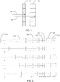
- FIG. 1 A first imager array 102 is positioned in a stacked configuration with a second imager array 104.
- the first imager array 102 captures a first portion of the incident light 106, while the second imager array 104 captures a second portion of the incident light 108 that passes through the first imaging array. It is noted that, while the portions of light are shown as distinct lines in FIG.
- these lines are intended to represent the portion of the overall incident light that is absorbed by each imager array.
- light from an object that is being imaged is captured on both imager arrays and will create different image patterns on each imager array that is a function of the distance from each imager array to the object. Differences in these image patterns can thus be utilized to obtain distance and/or 3D information about the object.
- a "light field” can be computed giving, for example, the light wavelength, intensity, and direction of light rays passing through the imager.
- Computations can then performed, in some cases in real time, by an on-chip processing unit or in a system processing unit to provide a variety of data, including visible image, IR image, range or distance to the object, 3D information, and the like.
- the object distance information collected can also be used to create a three dimensional image of the object.
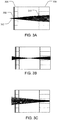
- FIG. 2 shows a side view schematic diagram of such three dimensional imaging at different distances, represented by rows 1-5.
- the imaging device can include a first imager array 202, a second imager array 204, and a system lens 206 for focusing incident light 208 onto the first and second imager arrays.
- a subject 210 is shown at a given distance for each of rows 1-5 from the imaging arrays.
- the boxes shown to the right of the imager arrays represent the imaging surface of each of the arrays, with the imaging surface for the first imaging array 202 being on the left and the imaging surface for the second imaging array 204 being on the right.
- the circle shown in each of the imaging surfaces represents the image patterns formed on each imaging surface of the subject 208 for a given distance. As is shown in FIG.
- the dimensions of the image patterns on the imaging surfaces change as a function of the distance to each imager array.
- the differences between the image patterns for a given distance can be utilized to calculate the distance to the subject.
- the change in distance to the subject can be repeatedly calculated.
- three dimensional representations can be obtained of subjects, including for subjects with complex surface contours or structures. In such cases, the three dimensional nature of a subject is reflected in the image pattern created on each of the imager arrays.
- the differences between image patterns from each array can be utilized to create a three dimensional representation.
- Such a representation can include three dimensional measurements of the subject, as well as three dimensional images.
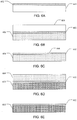
- FIGs. 3A-C where incident light 302 is shown passing through a first imager array 304 and a second imager array 306.
- the incident light 302 contacts the first imager array 304 with a first image pattern 308 that is related, at least in part, to the distance to the subject and the characteristics and distance of the system lens (not shown) from the first imager array 302.
- the second image pattern 310 is different from the first image pattern 308.
- the patterns will often differ in size between the two arrays, and the pixels that detect the pattern will be different between the two imager arrays. It is noted, however, that in some limited situations the patterns on both imager arrays will be the same size.
- the first and second image patterns concomitantly vary.
- the distance to a subject can be calculated based on the image feature difference between the first image pattern and the second image pattern of the stacked imager array, with known imager stack structure and system lens data.
- distance to a subject with a point or near-point source as well as image features can be calculated directly.
- Such point or near-point sources will generally produce simple image patters on each imager array.
- the effective image pattern radii of the first image pattern and the second image pattern can be determined as r1 and r2, respectively.
- focused images occur at a single plane with the best focal distance relative to the optics for specific subject. At this best focused location, the image is the sharpest with the smallest feature size for any image contents. At any other location, image will be defocused (a blurred image), with feature sizes that are bigger for the same image content at focused location.
- the smallest image feature size location is at the best focus location, where image is focused with minimum blur.
- an offset may be introduced to compensate for the difference in the distance from the front of the image array to the effective image plane.
- D the distance from the subject to the lens' principle plane
- f the focal length of the imaging lens
- s the distance from lens principle plane to the first image
- d the distance from the first image to the smallest image location.
- centroid xc sum x * pixel value / sum pixel value
- yc sum y * pixel value / sum pixel value
- the centroid xc and yc position is not limited by the pixel resolution, as x and y are pixel coordinates. Sub-pixel result can be used to achieve required calculation precision. The precision of the position can be sensor signal-to-noise ratio limited.
- image feature size can be determined by cross correlation between the inverse scaled first image and second image.
- the inverse scaled first image is processed by applying the inverse scale factor k to the image size (similar to a digital zoom). Again, the scaling is not pixel resolution limited, and sub-pixel scaling process is used to find the best correlated scale factor k with the highest correction result C.
- the best correlated scale factor k can then be used to describe the relationship between the first image and the second image.
- d is the image distance from first image to the smallest image size location
- t is the separation between first light incident surface and second light incident surface
- k is the scale factor applied to the first image in cross correlation.
- an offset may be introduced to compensate for the difference in the distance from the front of the image array to the effective image plane.
- D is the distance from the subject to the lens principle plane
- f is the focal length of the imaging lens
- s is the distance from lens principle plane to the first image
- d is the distance from first image to the smallest image location.
- a variety of configurations are contemplated for carrying out the calculations utilized to derive distance and/or three dimensional information from a subject.
- the calculations or at least a portion of the calculations can be performed on-chip with the imager arrays.
- a dedicated image processing unit can be utilized for the calculations or at least a portion of the calculations.
- the calculations or at least a portion of the calculations can be performed in a computing device.
- an imaging system capable of deriving three dimensional information from a three dimensional subject can, as is shown in FIG. 4 , include a first imager array 402 having a first light incident surface 404 and a second imager array 406 having a second light incident surface 408.
- the second imager array 406 is coupled to the first imager array 402 at a surface that is opposite the first light incident surface 404.
- the first imager array can be physically coupled to the second imager array.
- the first imager array can be optically coupled to the second imager array.
- the second light incident surface 408 is oriented toward the first imager array 402 and at least substantially uniformly spaced at a distance of from about 2 microns to about 150 microns from the first light incident surface.
- the system can additionally include a system lens 410 positioned to direct incident light 412 along an optical pathway 414 onto the first light incident surface 404.
- the system lens 410 can have a focal point 416 located in between the first light incident surface 404 and the second light incident surface 408, and/or in between the first imager array 402 and the second imager array 406.
- the first imager array 402 is operable to detect a first portion of the light passing along the optical pathway 414 and to pass through a second portion of the light
- the second imager array 406 is operable to detect at least a part of the second portion of light.
- the first portion of light and the second portion of light have at least one wavelength of from about 500 nm to about 1100 nm.
- the first portion of light and the second portion of light have at least one wavelength of from about 750 nm to about 1100 nm.
- the second portion of light includes at least substantially all wavelengths of light of from about 750 nm to about 1100 nm.
- first portion of light and the second portion of light have a center wavelength frequency between about 500 nm and about 1100 nm. In another aspect, the first portion of light and the second portion of light have a center wavelength frequency between about 750 nm and about 1100 nm.
- the wavelengths of light utilized by the stacked imager system can vary depending on, among other things, the design of the system and the intended application. In some aspects the same or substantially the same light wavelengths can be utilized by both the first imager array and the second imager array to derive distance and/or three dimensional information from the subject. In other aspects, different light wavelengths can be utilized by the first imager array than by the second imager array. While in many aspects IR light wavelengths are used to calculate three dimensional information about a subject, in some aspects visible light can be used to make such calculations.
- the imager arrays For example, assuming crystalline silicon imagers are utilized for the imager arrays, light in the visible spectrum of from about 500 nm to about 700 nm can be used, provided the first imaging array is sufficiently thin to allow a second portion of the visible light to pass there through. Furthermore, in some cases different wavelengths of light can be utilized differently in the system. For example, infrared light can be used by both the first imager array and the second imager array to generate a three dimensional representation or three dimensional image, while visible light can be captured by the first imager array in order to generate a visible image of the subject. When the two representations are combined, a resulting three dimensional visible image of the subject can be achieved.
- system can include an active illumination source, a first imager capable of detecting visible and infrared (IR) light and a second imager capable of detecting IR light.
- the system can further include an active illumination source capable of emitting IR light.
- the active illumination source, first imager and the second imager can pulsed at the same frequency such that the pulsed IR light is detected during the pulse window.
- the IR illumination source is off (i.e. in between pulses)
- the first image sensor is detecting and reading out visible light data.
- the one or more of the first and second imager arrays can include light filters that are capable of filtering out specific wavelengths of light or ranges of wavelengths of light.
- light having a certain wavelength or wavelength range can be concentrated by a structure such as a system lens on a specific imager array or even a portion of an imager array.
- an IR cut filter (moveable) or notch filter can be employed in front one or more pixels of the first imager array.
- Such a filter can pass infrared light that will be used in range or distance determination and filter out light in the visible range.
- a long-pass filter can pass both infrared and visible red light.
- a long-pass filter can be utilized that passes green, red, and infrared light.
- a band-pass filter can be used that passes visible light and specific wavelengths of IR light, such as, for example, 850 nm, 940 nm, and/or 1064 nm light, while blocking all other wavelengths.
- the system can include a focusing system for altering the focal plane(s) of the imaging system. While various techniques are contemplated, in one aspect the distance of the first imager array from the second imager array can be varied by, for example, piezoelectric materials.
- the system can additionally include an active light emitter configured to emit active light radiation at least substantially toward the subject. While any light can be utilized as an active light source, in one aspect the active light source can emit light having a center wavelength in the infrared range. In another aspect, the emitted light can have a center wavelength of from about 750 nm to about 1100 nm. In yet another aspect, the active light radiation can have a center frequency selected from 850 nm, 940 nm, 1064 nm, or a combination thereof.
- the system can include a computational module that is operable to calculate distance data from the imaging system to the three dimensional subject using first image data collected by the first imager array from the first portion of light and second image data collected by the second imager array from the second portion of light.
- Computational modules are well known, and can include various processing units, data storage, memory, I/O functionality, and the like.
- the computation module is capable of generating a three dimensional representation of the subject from the distance data.
- the computational module can generate a three dimensional image from the data derived from the first imager array and the second imager array.
- the imaging system can be incorporated into a computing system operable to alter computation based on variations in distance data derived from movements of a subject.
- motions made by the subject can be captured by the imaging system and used by the computing system to alter the computation of the computing system.
- computation of the computing system can be varied according to the motion of an oncoming vehicle or other moving subject.
- each of the first and second imager array is made up of a plurality of pixels.
- the pixels can be architecturally configured as front-side illuminated pixels or back-side illuminated pixels.
- all of the first imager array pixels and the second imager array pixels can be front-side illuminated pixels.
- all of the first imager array pixels can be front-side illuminated and all of the second imager array pixels can be backside illuminated pixels. Additionally, it is contemplated that in some aspects either of the first or second imager arrays can be front-side illuminated while the other imager array can be backside illuminated.
- a system can include a texture region 502 coupled to the second imager array 406 on a side opposite the first imager array 402.
- the textured region 502 is positioned to redirect light passing through the second imager array 406 back into the second imager array 406.
- the light passing through the second imager array is shown at 504, and the light redirected back into the imager array is shown at 506.
- the textured region 502 can be formed across all or substantially all of the back surface of the second imager array 406, or the textured region 502 can be formed on a portion thereof.
- the textured region can be formed at the level of the pixels that make up the imager array, and as such, can be formed on a portion of the pixel surface, substantially all of the pixel surface, or all of the pixel surface. Also, it is noted that callout numbers used in FIG. 5 from previous figures denote the same or similar structures as the previous figure. Furthermore, in some aspects a textured region is explicitly disclaimed from being applied to the first imager array, while in other aspects such a textured region can be utilized.
- the textured region can function to diffuse electromagnetic radiation, to redirect electromagnetic radiation, and/or to absorb electromagnetic radiation, thus increasing the efficiency of the second imager array.
- the textured region can include surface features to thus increase the optical path length of the second imager array.
- Such surface features can be micron-sized and/or nano-sized, and can be any shape or configurations. Non-limiting examples of such shapes and configurations include cones, pillars, pyramids, micolenses, quantum dots, inverted features, gratings, protrusions, and the like, including combinations thereof.
- factors such as manipulating the feature sizes, dimensions, material type, dopant profiles, texture location, etc. can allow the diffusing region to be tunable for a specific wavelength or wavelength range.
- tuning the device can allow specific wavelengths or ranges of wavelengths to be absorbed.
- textured regions can also allow an imager array to experience multiple passes of incident electromagnetic radiation within the device, particularly at longer wavelengths (i.e. infrared). Such internal reflection increases the optical path length to be greater than the thickness of the semiconductor. This increase in the optical path length increases the quantum efficiency of the device, leading to an improved signal to noise ratio.
- the textured region can be formed by various techniques, including plasma etching, reactive ion etching, porous silicon etching, lasing, chemical etching (e.g. anisotropic etching, isotropic etching), nanoimprinting, material deposition, selective epitaxial growth, shallow trench isolation, and the like.
- One effective method of producing a textured region is through laser processing. Such laser processing allows discrete locations of the imager array or other substrate to be textured.
- a variety of techniques of laser processing to form a textured region are contemplated, and any technique capable of forming such a region should be considered to be within the present scope. Examples of such processing have been described in further detail in U.S. Patents 7,057,256 , 7,354,792 and 7,442,629 . Briefly, a surface of a substrate material is irradiated with laser radiation to form a textured or surface modified region.
- the type of laser radiation used to surface modify a material can vary depending on the material and the intended modification. Any laser radiation known in the art can be used with the devices and methods of the present disclosure. There are a number of laser characteristics, however, that can affect the texturing process and/or the resulting product including, but not limited to the wavelength of the laser radiation, pulse width, pulse fluence, pulse frequency, polarization, laser propagation direction relative to the semiconductor material, etc.
- a laser can be configured to provide pulsatile lasing of a material.
- a short-pulsed laser is one capable of producing femtosecond, picosecond and/or nanosecond pulse durations.
- Laser pulses can have a central wavelength in a range of about from about 10 nm to about 8 ⁇ m, and more specifically from about 200 nm to about 1200 nm.
- the pulse width of the laser radiation can be in a range of from about tens of femtoseconds to about hundreds of nanoseconds.
- laser pulse widths can be in the range of from about 50 femtoseconds to about 50 picoseconds.
- laser pulse widths can be in the range of from about 50 picoseconds to 100 nanoseconds.
- laser pulse widths are in the range of from about 50 to 500 femtoseconds.
- laser pulse widths are in the range of from about 10 femtoseconds to about 500 picoseconds.
- the number of laser pulses irradiating a target region can be in a range of from about 1 to about 2000. In one aspect, the number of laser pulses irradiating a target region can be from about 2 to about 1000. Further, the repetition rate or frequency of the pulses can be selected to be in a range of from about 10 Hz to about 10 ⁇ Hz, or in a range of from about 1 kHz to about 1 MHz, or in a range from about 10 Hz to about 1 kHz. Moreover, the fluence of each laser pulse can be in a range of from about 1 kJ/m 2 to about 20 kJ/m 2 , or in a range of from about 3 kJ/m 2 to about 8 kJ/m 2 .
- an imaging system can further include a reflector coupled to the second imager array on a side opposite the first imager array.
- the reflector can be positioned to reflect light passing through the second imager array back into the second imager array.
- Numerous reflector materials are contemplated, and can include any material or composite of materials that can function to reflect light. Non-limiting examples of such materials can include metals, metal alloys, ceramics, polymers, glass, quartz, Bragg-type reflectors, and the like.
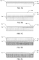
- FIGs. 6A-E show various steps in the non-limiting manufacture of a stacked imager structure according to one aspect of the present disclosure.
- first imager array 602 is formed on the front side of a semiconductor layer 604.
- the first imager array 602 can include any form of imager array that can be incorporated into an imager system, and any such device is considered to be within the present scope.
- a variety of semiconductor materials are contemplated for use as the semiconductor layer of the devices and methods according to aspects of the present disclosure. As such, any semiconductor material that can be used in a stacked imager device is considered to be within the present scope.
- Non-limiting examples of such semiconductor materials can include group IV materials, compounds and alloys comprised of materials from groups II and VI, compounds and alloys comprised of materials from groups III and V, and combinations thereof. More specifically, exemplary group IV materials can include silicon, carbon (e.g. diamond), germanium, and combinations thereof. Various exemplary combinations of group IV materials can include silicon carbide (SiC) and silicon germanium (SiGe).
- the semiconductor material can be silicon.
- the semiconductor layer can be a silicon wafer. The silicon wafer/material can be monocrystalline, multicrystalline, microcrystalline, amorphous, and the like. In one specific aspect, the silicon material can be a monocrystalline silicon wafer.
- a carrier substrate (or handle) 606 can be bonded to the first imager array 602. Note that in FIG. 6B , the device has been flipped or rotated 180° as compared to FIG. 6A .
- the carrier substrate can include a variety of materials. Because in many aspects the carrier substrate 606 is a temporary substrate to be removed at a later processing step, the material can be chosen based on its usefulness as a temporary substrate. It can also be beneficial for the carrier substrate 606 to be capable of adequately holding the first imager array 602 during processing of the semiconductor layer 604 and yet be capable of easy removal.
- Non-limiting examples of potential carrier substrate materials can include glass, ceramics, semiconductors, and the like, including combinations thereof.
- Various bonding techniques are contemplated for attaching the carrier substrate 606 to the first imager array 602, and any such bonding technique useful in making a stacked imager device is considered to be within the present scope.
- One such process can include a liquid UV curable adhesive process that utilizes solids acrylic adhesives designed for temporary bonding of semiconductor wafers to a glass carrier substrate. This technique provides a rigid, uniform support surface that minimizes stress on the wafer during the subsequent processing steps, resulting in less warpage, cracking, edge chipping and higher yields.
- Other exemplary methods can include bonding and detaching a temporary carrier used for handling a wafer during the fabrication of semiconductor devices, includes bonding the wafer onto the carrier through an adhesive layer.
- bonding at low or room temperature can include surface cleaning and activation by cleaning or etching, followed by polishing the surfaces to be bonded to a high degree of smoothness and planarity. Reactive ion etching or wet etching is used to slightly etch the surfaces being bonded. The etched surfaces may be rinsed in solutions such as ammonium hydroxide or ammonium fluoride to promote the formation of desired bonding species on the surfaces.
- the first imager array 602 and the carrier substrate 606 can be bonded at room temperature and a thermal treatment can be applied to consolidate the bonding interface.
- the parameters of the consolidation annealing can be controlled to provide a bonding energy high enough for the heterostructure to withstand post- bonding conventional process steps (e.g. CMOS processing).
- the bonding technique can include various oxide-oxide, oxide-silicon, or metal-metal bonding methods.
- Some bonding processes can achieve a bond strength of at least 1 J/m 2 at room temperature. For even higher bond strengths, a bake cycle at 100° - 300° C can be utilized. Some of these oxide-oxide bonding process have been described in U.S. Patent 7,871,898 and U.S. Patent 5,843 , One method of direct bonding a silicon wafer onto an insulated wafer in order to obtain a stacked imager device is similar to the bonding of two silicon wafers together, with the exception that before bonding a thin thermal oxide layer (e.g. about 1 micron) is grown on one of the wafers.
- a thin thermal oxide layer e.g. about 1 micron
- Release of the carrier substrate from the device layer can vary depending on the attachment process.
- Acrylic adhesives for example, can be released by exposure to UV light.
- More permanent bonds, such as silicon-oxide bonds may require the removal of the carrier substrate by mechanical grinding and/or chemical etching to expose the device layer.
- the semiconductor layer 604 ( FIG. 6B ) is at least partially removed (e.g. polished and thinned) to expose the backside of the first imager array 602 or, in other words, to form a processed surface 608 at the backside of the first imager array 602.
- the resulting structure is comprised of the first substrate 606 coupled to the first imager array 602.
- any necessary or beneficial backside processing can be performed on the processed surface 608 of the first imager array 602.
- beneficial backside processing can include, without limitation, shallow or deep trench formation, via formation, annealing, implantation, and the like.
- backside processing can also include exposing contact pads associated with the first imager array.
- opening the backside of the device layer i.e. at the processed surface
- electrical contacts can be exposed for bonding and providing electrical contact to subsequent structures, such as the second imager array (see below).
- Opening the backside can occur by any known technique, including the thinning and processing methods described. In one specific aspect, opening the backside can be accomplished via plasma etching.
- any technique useful for removing the semiconductor layer 604 is considered to be within the present scope.
- Non-limiting examples can include ion implantation/separation processes, laser ablation, laser splitting, CMP processing, dry etching, wet etching and the like, including combinations thereof.
- the semiconductor layer is removed by CMP techniques to expose the device layer 602.
- a second imager array 610 is bonded to the backside of the first imager array 602, as is shown in FIG. 6D .
- the device has been flipped or rotated by 180° compared to FIG. 6C .
- Any bonding technique can be utilized to bond the second imager array 210 to the first imager array 202, as was described for the bonding of the first substrate 206 to the first imager array 202 ( FIG. 6B ), provided the process is compatible with both structures.
- any spacing that exists between the first and second imager arrays can be filled with a light transparent material such as amorphous silicon, an oxide, nitride, or the like.
- an air gap can be maintained between the first and second imager arrays. Such a gap can be filled with actual air, an inert gas, a vacuum, etc.
- first imager array and the second imager array can be electrically coupled to, and thus can function in conjunction with, one another. Such electrical coupling can be accomplished by vias formed through the processed surface that connect the two imager arrays.
- the carrier substrate 606 ( FIG. 6D ) can be removed from the first imager array 602 following bonding of the second imager array 610.
- the resulting stacked imager structure shown in FIG. 6E includes a second imager array 610 bonded to a first imager array 602.
- FIGs. 7A-E show various steps in the manufacture of a stacked imager device using an embedded oxide layer to facilitate thinning and creating a space between the imager arrays.
- first imager array 702 can be formed on the front side of a semiconductor layer 704.
- the first imager array 702 can include any form of imager array that can be incorporated into a stacked imager device, as has been described.
- a thin oxide layer 703 can be embedded within the semiconductor layer 704, either before or after the formation of the first imager array 702.
- the thin oxide layer can be of any shape and thickness useful for the particular device design. In some aspects, however, the thin oxide layer can be from about 4000 angstroms to about 1.5 microns thick. It is also noted that commercial SOI substrates can be used that are manufactured having such a thin oxide layer embedded.
- a carrier substrate 706 can be bonded to the first imager array 702. Note that in FIG. 7B , the device has been flipped or rotated 180° as compared to FIG. 7A .
- the carrier substrate can include a variety of materials. Because in most aspects the carrier substrate 706 is a temporary substrate to be removed at a later processing step, the material can be chosen based on its usefulness as a temporary substrate.
- the semiconductor layer 704 ( FIG. 7B ) is at least partially removed to form a processed surface 708 near the backside of the first imager array 702.
- the semiconductor layer 704 can be removed at least to the thin oxide layer 703.
- at least a portion of the thin oxide layer can remain, while in other aspects the thin oxide layer can be completely removed from the semiconductor layer.
- This material can be removed by any known method, such as, for example, laser splitting, polishing, thinning, etching, lapping or grinding, CMP processing, or a combination thereof.
- the resulting structure is comprised of the carrier substrate 706 coupled to the first imager array 702.
- a portion of the semiconductor layer 704 can remain coupled to the first imager array 702 opposite the carrier substrate 706.
- processing the semiconductor layer on the backside can include implant and/or laser anneal conditions to reduce surface defects.
- a second imager array 710 can be bonded to the semiconductor layer 704 at backside of the first imager array 702, as is shown in FIG. 7D .
- the device has been flipped or rotated 180° compared to FIG. 7C . Any bonding technique can be utilized to bond the second imager array 710 to the semiconductor layer 704, as has been described.
- the carrier substrate 706 ( FIG. 7D ) can be removed from the first imager array 702 following bonding of the second imager array 710.
- the resulting stacked imager structure shown in FIG. 7E includes a second imager array 710 bonded to the semiconductor layer 704, which is bonded to the first imager array 702. It is noted that the distance between the imagers can be varied during manufacture by varying the thickness of the semiconductor layer 704 that remains and is bonded between the imager arrays.
- the present disclosure additionally provides methods of determining distance to a subject.
- a method can include focusing incident light along an optical pathway onto a first light incident surface of a first imaging array, where the first imaging array captures a first portion of the light having at least one wavelength of from about 500 nm to about 1100 nm to generate a first data set and passes through a second portion of the light along the optical pathway.
- the method can also include receiving the second portion of the light onto a second light incident surface of a second imaging array, where the second imaging array captures the second portion of the light having at least one wavelength of from about 500 nm to about 1100 nm to generate a second data set.
- the distance to the subject can be derived from variations between the first data set and the second data set.
- the method can also include redirecting at least part of the second portion of the light that passes through the second imaging array back into the second imaging array.
- the present disclosure provides an imaging system capable of deriving three dimensional information from a three dimensional subject.
- a system can include an active illumination source capable of emitting pulsed infrared light, a first imager capable of detecting visible and infrared light, and a second imager capable of detecting infrared light.
- the active illumination source, first imager, and the second imager can be pulsed at a frequency and duty cycle such that the pulsed infrared light is detected by the first imager and the second imager when the active illumination is on.
- the first imager is operable to detect visible light when the active illumination source is in an off state.
Landscapes
- Engineering & Computer Science (AREA)
- Multimedia (AREA)
- Signal Processing (AREA)
- Physics & Mathematics (AREA)
- General Physics & Mathematics (AREA)
- Computer Vision & Pattern Recognition (AREA)
- Theoretical Computer Science (AREA)
- Length Measuring Devices By Optical Means (AREA)
- Measurement Of Optical Distance (AREA)
Claims (13)
- Système d'imagerie permettant de dériver des informations tridimensionnelles à partir d'un sujet tridimensionnel, comprenant :un premier réseau imageur (402) ayant une première surface d'incidence de lumière (404) ;un deuxième réseau imageur (406) ayant une deuxième surface d'incidence de lumière (408), le deuxième réseau imageur (406) étant couplé au premier réseau imageur (402) au niveau d'une surface qui est opposée à la première surface d'incidence de lumière (404), la deuxième surface d'incidence de lumière (408) étant orientée vers le premier réseau imageur (402) et au moins espacée sensiblement uniformément d'une distance comprise entre 2 microns et 150 microns de la première surface d'incidence de lumière (404) ;une lentille du système (410) positionnée pour diriger la lumière d'incidence le long d'un trajet optique (414) sur la première surface d'incidence de lumière (404),dans lequel le premier réseau imageur (402) peut être utilisé pour détecter une première partie de la lumière passant le long du trajet optique (414) et pour passer à travers une deuxième partie de la lumière,dans lequel le deuxième réseau imageur (406) peut être utilisé pour détecter au moins une partie de la deuxième partie de la lumière, et dans lequel la première partie de la lumière et la deuxième partie de la lumière ont une ou plusieurs longueurs d'onde comprises entre 500 nm et 1100 nm ; etun module de calcul configuré pour recevoir des premières données d'image collectées par le premier réseau imageur (402) dans la première partie de la lumière et des deuxièmes données d'image collectées par le deuxième réseau imageur (406) dans la deuxième partie de la lumière,dans lequel le module de calcul peut être utilisé pour calculer des données de distance du système d'imagerie au sujet tridimensionnel comme suit :calculer les rayons caractéristiques efficaces d'une image défocalisée à partir du volume total des valeurs de pixel d'image en utilisant les équations :

 calculer l'emplacement de la dimension d'image la plus petite à partir des premières données d'image sur la base des rayons caractéristiques du premier motif d'image et du deuxième motif d'image en utilisant l'équation :
 calculer la distance du système d'imagerie au sujet tridimensionnel en utilisant une équation d'imagerie à lentille :
- Système d'imagerie selon la revendication 1, dans lequel la première partie de la lumière et la deuxième partie de la lumière ont une ou plusieurs longueurs d'onde comprises entre 750 nm et 1100 nm.
- Système d'imagerie selon la revendication 1, dans lequel la distance entre la première surface d'incidence de lumière (404) et la deuxième surface d'incidence de lumière (408) est comprise entre 10 microns et 100 microns.
- Système d'imagerie selon la revendication 1, dans lequel le premier réseau imageur (402) peut être utilisé pour capturer une image de lumière visible.
- Système d'imagerie selon la revendication 1, dans lequel le premier réseau imageur inclut une pluralité de pixels configuré architecturalement sous forme de pixels éclairés par la face avant.
- Système d'imagerie selon la revendication 1, comprenant en outre une région texturée (502) couplée au deuxième réseau imageur (406) sur un côté opposé au premier réseau imageur (402), dans lequel la région texturée (502) est positionnée pour rediriger la lumière passant à travers le deuxième réseau imageur (406) dans le deuxième réseau imageur (406) ; ou comprenant en outre un réflecteur couplé au deuxième réseau imageur (406) sur un côté opposé au premier réseau imageur (402), dans lequel le réflecteur est positionné pour réfléchir la lumière passant à travers le deuxième réseau imageur (406) dans le deuxième réseau imageur (406).
- Système d'imagerie selon la revendication 1, dans lequel la lentille du système (410) a un point focal situé entre la première surface d'incidence de lumière (404) et la deuxième surface d'incidence de lumière (408).
- Système d'imagerie selon la revendication 2, dans lequel le système d'imagerie comprend en outre un émetteur de lumière actif configuré pour émettre un rayonnement lumineux actif au moins sensiblement vers le sujet tridimensionnel et ayant une longueur d'onde centrale comprise entre 750 nm et 1100 nm.
- Système d'imagerie selon la revendication 8, dans lequel le rayonnement lumineux actif a une fréquence centrale sélectionnée dans le groupe constitué de 850 nm, 940 nm et 1064 nm.
- Système d'imagerie selon la revendication 8, dans lequel l'émetteur de lumière actif est capable d'émettre une lumière pulsée, et dans lequel l'émetteur de lumière actif, le premier réseau imageur (402) et le deuxième réseau imageur (406) sont puisés à une fréquence et un cycle d'utilisation tels que la lumière infrarouge puisée est détectée par le premier réseau imageur (402) et le deuxième réseau imageur (406) quand l'émetteur de lumière actif est activé.
- Système d'imagerie selon la revendication 10, dans lequel le premier réseau imageur (402) peut être utilisé pour détecter la lumière visible quand l'émetteur de lumière actif est dans un état désactivé.
- Système d'imagerie selon la revendication 1, dans lequel le système d'imagerie est incorporé dans un système informatique pouvant être utilisé pour modifier le calcul sur la base de variations dans des données de distance dérivées des mouvements d'un sujet.
- Système d'imagerie selon la revendication 1, dans lequel le premier réseau imageur (402) inclut une pluralité de pixels configurés architecturalement sous forme de pixels éclairés par la face avant et dans lequel le deuxième réseau imageur (406) inclut une pluralité de pixels configurés architecturalement sous forme de pixels éclairés par la face avant ou de pixels éclairés par la face arrière.
Applications Claiming Priority (2)
| Application Number | Priority Date | Filing Date | Title |
|---|---|---|---|
| US201361798805P | 2013-03-15 | 2013-03-15 | |
| PCT/US2014/024964 WO2014151093A1 (fr) | 2013-03-15 | 2014-03-12 | Imagerie tridimensionnelle utilisant des dispositifs imageurs empilés et procédés associés |
Publications (3)
| Publication Number | Publication Date |
|---|---|
| EP2974302A1 EP2974302A1 (fr) | 2016-01-20 |
| EP2974302A4 EP2974302A4 (fr) | 2016-11-16 |
| EP2974302B1 true EP2974302B1 (fr) | 2019-05-01 |
Family
ID=52718346
Family Applications (1)
| Application Number | Title | Priority Date | Filing Date |
|---|---|---|---|
| EP14768046.6A Active EP2974302B1 (fr) | 2013-03-15 | 2014-03-12 | Imagerie tridimensionnelle utilisant des dispositifs imageurs empilés et procédés associés |
Country Status (2)
| Country | Link |
|---|---|
| EP (1) | EP2974302B1 (fr) |
| TW (1) | TWI661173B (fr) |
Family Cites Families (7)
| Publication number | Priority date | Publication date | Assignee | Title |
|---|---|---|---|---|
| WO2010019161A1 (fr) * | 2008-08-15 | 2010-02-18 | Sionyx, Inc. | Détecteur de lumière semi-conducteur à large bande |
| JP5961332B2 (ja) * | 2009-09-17 | 2016-08-02 | サイオニクス、エルエルシー | 感光撮像素子および関連方法 |
| US20120300037A1 (en) * | 2010-02-03 | 2012-11-29 | Battelle Memorial Institute | Three-dimensional imaging system using a single lens system |
| TWI396824B (zh) * | 2010-03-02 | 2013-05-21 | Witrins S R O | 用於光學測量產品表面之方法及器件 |
| WO2011150551A1 (fr) * | 2010-06-01 | 2011-12-08 | 博立码杰通讯(深圳)有限公司 | Dispositif photosensible multispectral |
| KR101572020B1 (ko) * | 2011-06-24 | 2015-11-26 | 볼리 미디어 커뮤니케이션스 (센젠) 캄파니 리미티드 | 다중 피사계 심도 감광소자, 시스템, 피사계 심도 확장방법 및 광학 화상 시스템 |
| US9136300B2 (en) * | 2013-01-11 | 2015-09-15 | Digimarc Corporation | Next generation imaging methods and systems |
-
2014
- 2014-03-12 EP EP14768046.6A patent/EP2974302B1/fr active Active
- 2014-03-14 TW TW103109579A patent/TWI661173B/zh active
Non-Patent Citations (1)
| Title |
|---|
| XIONG Y ET AL: "Depth from focusing and defocusing", COMPUTER VISION AND PATTERN RECOGNITION, 1993. PROCEEDINGS CVPR '93., 1993 IEEE COMPUTER SOCIETY CONFERENCE ON NEW YORK, NY, USA 15-17 JUNE, LOS ALAMITOS, CA, USA,IEEE COMPUT. SOC, 15 June 1993 (1993-06-15), pages 68 - 73, XP010095843, ISBN: 978-0-8186-3880-0, DOI: 10.1109/CVPR.1993.340977 * |
Also Published As
| Publication number | Publication date |
|---|---|
| EP2974302A1 (fr) | 2016-01-20 |
| TW201502463A (zh) | 2015-01-16 |
| TWI661173B (zh) | 2019-06-01 |
| EP2974302A4 (fr) | 2016-11-16 |
Similar Documents
| Publication | Publication Date | Title |
|---|---|---|
| US9939251B2 (en) | Three dimensional imaging utilizing stacked imager devices and associated methods | |
| US20190222778A1 (en) | Biometric imaging devices and associated methods | |
| US20130168792A1 (en) | Three Dimensional Architecture Semiconductor Devices and Associated Methods | |
| CN105308626A (zh) | 生物识别成像装置以及其方法 | |
| US20150356351A1 (en) | Biometric Imaging Devices and Associated Methods | |
| TWI605579B (zh) | 具有非平坦光學介面之背側照明影像感測器 | |
| WO2012122572A2 (fr) | Capteurs tridimensionnels, systèmes et procédés associés | |
| CN113206115B (zh) | 操作装置的方法、半导体结构以及影像感测器 | |
| EP2583312A2 (fr) | Dispositifs photosensibles à grande vitesse et procédés associés | |
| JP2009507392A (ja) | 集積レンズスタックを備えた裏面薄化イメージセンサ | |
| US20250318302A1 (en) | Transparent refraction structure for an image sensor and methods of forming the same | |
| CN110634895B (zh) | 使用热塑性衬底材料的弯曲图像传感器 | |
| EP2974302B1 (fr) | Imagerie tridimensionnelle utilisant des dispositifs imageurs empilés et procédés associés | |
| WO2013056249A1 (fr) | Dispositifs semi-conducteurs à architecture tridimensionnelle et procédés associés | |
| TWI810632B (zh) | 短波紅外線焦點平面陣列及其使用方法和製造方法 | |
| JP2018107314A (ja) | 光検知器及び撮像装置 | |
| CN117153853A (zh) | 光电传感器及其形成方法、电子设备 |
Legal Events
| Date | Code | Title | Description |
|---|---|---|---|
| PUAI | Public reference made under article 153(3) epc to a published international application that has entered the european phase |
Free format text: ORIGINAL CODE: 0009012 |
|
| 17P | Request for examination filed |
Effective date: 20150918 |
|
| AK | Designated contracting states |
Kind code of ref document: A1 Designated state(s): AL AT BE BG CH CY CZ DE DK EE ES FI FR GB GR HR HU IE IS IT LI LT LU LV MC MK MT NL NO PL PT RO RS SE SI SK SM TR |
|
| AX | Request for extension of the european patent |
Extension state: BA ME |
|
| DAX | Request for extension of the european patent (deleted) | ||
| RIC1 | Information provided on ipc code assigned before grant |
Ipc: H04N 13/02 20060101AFI20160706BHEP Ipc: H01L 27/146 20060101ALI20160706BHEP |
|
| A4 | Supplementary search report drawn up and despatched |
Effective date: 20161017 |
|
| RIC1 | Information provided on ipc code assigned before grant |
Ipc: H04N 13/02 20060101AFI20161011BHEP Ipc: H01L 27/146 20060101ALI20161011BHEP |
|
| STAA | Information on the status of an ep patent application or granted ep patent |
Free format text: STATUS: EXAMINATION IS IN PROGRESS |
|
| 17Q | First examination report despatched |
Effective date: 20180308 |
|
| REG | Reference to a national code |
Ref country code: DE Ref legal event code: R079 Ref document number: 602014045810 Country of ref document: DE Free format text: PREVIOUS MAIN CLASS: H04N0013020000 Ipc: H04N0013200000 |
|
| GRAP | Despatch of communication of intention to grant a patent |
Free format text: ORIGINAL CODE: EPIDOSNIGR1 |
|
| STAA | Information on the status of an ep patent application or granted ep patent |
Free format text: STATUS: GRANT OF PATENT IS INTENDED |
|
| RIC1 | Information provided on ipc code assigned before grant |
Ipc: H04N 13/20 20160120AFI20181016BHEP |
|
| INTG | Intention to grant announced |
Effective date: 20181107 |
|
| RIC1 | Information provided on ipc code assigned before grant |
Ipc: H04N 13/20 20180101AFI20181016BHEP |
|
| RIC1 | Information provided on ipc code assigned before grant |
Ipc: H04N 13/20 20180101AFI20181016BHEP |
|
| GRAS | Grant fee paid |
Free format text: ORIGINAL CODE: EPIDOSNIGR3 |
|
| GRAA | (expected) grant |
Free format text: ORIGINAL CODE: 0009210 |
|
| STAA | Information on the status of an ep patent application or granted ep patent |
Free format text: STATUS: THE PATENT HAS BEEN GRANTED |
|
| AK | Designated contracting states |
Kind code of ref document: B1 Designated state(s): AL AT BE BG CH CY CZ DE DK EE ES FI FR GB GR HR HU IE IS IT LI LT LU LV MC MK MT NL NO PL PT RO RS SE SI SK SM TR |
|
| REG | Reference to a national code |
Ref country code: GB Ref legal event code: FG4D |
|
| REG | Reference to a national code |
Ref country code: CH Ref legal event code: EP Ref country code: AT Ref legal event code: REF Ref document number: 1128504 Country of ref document: AT Kind code of ref document: T Effective date: 20190515 |
|
| REG | Reference to a national code |
Ref country code: DE Ref legal event code: R096 Ref document number: 602014045810 Country of ref document: DE |
|
| REG | Reference to a national code |
Ref country code: IE Ref legal event code: FG4D |
|
| REG | Reference to a national code |
Ref country code: NL Ref legal event code: MP Effective date: 20190501 |
|
| REG | Reference to a national code |
Ref country code: LT Ref legal event code: MG4D |
|
| PG25 | Lapsed in a contracting state [announced via postgrant information from national office to epo] |
Ref country code: LT Free format text: LAPSE BECAUSE OF FAILURE TO SUBMIT A TRANSLATION OF THE DESCRIPTION OR TO PAY THE FEE WITHIN THE PRESCRIBED TIME-LIMIT Effective date: 20190501 Ref country code: HR Free format text: LAPSE BECAUSE OF FAILURE TO SUBMIT A TRANSLATION OF THE DESCRIPTION OR TO PAY THE FEE WITHIN THE PRESCRIBED TIME-LIMIT Effective date: 20190501 Ref country code: FI Free format text: LAPSE BECAUSE OF FAILURE TO SUBMIT A TRANSLATION OF THE DESCRIPTION OR TO PAY THE FEE WITHIN THE PRESCRIBED TIME-LIMIT Effective date: 20190501 Ref country code: SE Free format text: LAPSE BECAUSE OF FAILURE TO SUBMIT A TRANSLATION OF THE DESCRIPTION OR TO PAY THE FEE WITHIN THE PRESCRIBED TIME-LIMIT Effective date: 20190501 Ref country code: PT Free format text: LAPSE BECAUSE OF FAILURE TO SUBMIT A TRANSLATION OF THE DESCRIPTION OR TO PAY THE FEE WITHIN THE PRESCRIBED TIME-LIMIT Effective date: 20190901 Ref country code: NO Free format text: LAPSE BECAUSE OF FAILURE TO SUBMIT A TRANSLATION OF THE DESCRIPTION OR TO PAY THE FEE WITHIN THE PRESCRIBED TIME-LIMIT Effective date: 20190801 Ref country code: AL Free format text: LAPSE BECAUSE OF FAILURE TO SUBMIT A TRANSLATION OF THE DESCRIPTION OR TO PAY THE FEE WITHIN THE PRESCRIBED TIME-LIMIT Effective date: 20190501 Ref country code: ES Free format text: LAPSE BECAUSE OF FAILURE TO SUBMIT A TRANSLATION OF THE DESCRIPTION OR TO PAY THE FEE WITHIN THE PRESCRIBED TIME-LIMIT Effective date: 20190501 Ref country code: NL Free format text: LAPSE BECAUSE OF FAILURE TO SUBMIT A TRANSLATION OF THE DESCRIPTION OR TO PAY THE FEE WITHIN THE PRESCRIBED TIME-LIMIT Effective date: 20190501 |
|
| PG25 | Lapsed in a contracting state [announced via postgrant information from national office to epo] |
Ref country code: BG Free format text: LAPSE BECAUSE OF FAILURE TO SUBMIT A TRANSLATION OF THE DESCRIPTION OR TO PAY THE FEE WITHIN THE PRESCRIBED TIME-LIMIT Effective date: 20190801 Ref country code: RS Free format text: LAPSE BECAUSE OF FAILURE TO SUBMIT A TRANSLATION OF THE DESCRIPTION OR TO PAY THE FEE WITHIN THE PRESCRIBED TIME-LIMIT Effective date: 20190501 Ref country code: LV Free format text: LAPSE BECAUSE OF FAILURE TO SUBMIT A TRANSLATION OF THE DESCRIPTION OR TO PAY THE FEE WITHIN THE PRESCRIBED TIME-LIMIT Effective date: 20190501 Ref country code: GR Free format text: LAPSE BECAUSE OF FAILURE TO SUBMIT A TRANSLATION OF THE DESCRIPTION OR TO PAY THE FEE WITHIN THE PRESCRIBED TIME-LIMIT Effective date: 20190802 |
|
| REG | Reference to a national code |
Ref country code: AT Ref legal event code: MK05 Ref document number: 1128504 Country of ref document: AT Kind code of ref document: T Effective date: 20190501 |
|
| PG25 | Lapsed in a contracting state [announced via postgrant information from national office to epo] |
Ref country code: IS Free format text: LAPSE BECAUSE OF FAILURE TO SUBMIT A TRANSLATION OF THE DESCRIPTION OR TO PAY THE FEE WITHIN THE PRESCRIBED TIME-LIMIT Effective date: 20190901 |
|
| PG25 | Lapsed in a contracting state [announced via postgrant information from national office to epo] |
Ref country code: SK Free format text: LAPSE BECAUSE OF FAILURE TO SUBMIT A TRANSLATION OF THE DESCRIPTION OR TO PAY THE FEE WITHIN THE PRESCRIBED TIME-LIMIT Effective date: 20190501 Ref country code: EE Free format text: LAPSE BECAUSE OF FAILURE TO SUBMIT A TRANSLATION OF THE DESCRIPTION OR TO PAY THE FEE WITHIN THE PRESCRIBED TIME-LIMIT Effective date: 20190501 Ref country code: DK Free format text: LAPSE BECAUSE OF FAILURE TO SUBMIT A TRANSLATION OF THE DESCRIPTION OR TO PAY THE FEE WITHIN THE PRESCRIBED TIME-LIMIT Effective date: 20190501 Ref country code: AT Free format text: LAPSE BECAUSE OF FAILURE TO SUBMIT A TRANSLATION OF THE DESCRIPTION OR TO PAY THE FEE WITHIN THE PRESCRIBED TIME-LIMIT Effective date: 20190501 Ref country code: CZ Free format text: LAPSE BECAUSE OF FAILURE TO SUBMIT A TRANSLATION OF THE DESCRIPTION OR TO PAY THE FEE WITHIN THE PRESCRIBED TIME-LIMIT Effective date: 20190501 Ref country code: RO Free format text: LAPSE BECAUSE OF FAILURE TO SUBMIT A TRANSLATION OF THE DESCRIPTION OR TO PAY THE FEE WITHIN THE PRESCRIBED TIME-LIMIT Effective date: 20190501 |
|
| REG | Reference to a national code |
Ref country code: DE Ref legal event code: R097 Ref document number: 602014045810 Country of ref document: DE |
|
| PG25 | Lapsed in a contracting state [announced via postgrant information from national office to epo] |
Ref country code: SM Free format text: LAPSE BECAUSE OF FAILURE TO SUBMIT A TRANSLATION OF THE DESCRIPTION OR TO PAY THE FEE WITHIN THE PRESCRIBED TIME-LIMIT Effective date: 20190501 Ref country code: IT Free format text: LAPSE BECAUSE OF FAILURE TO SUBMIT A TRANSLATION OF THE DESCRIPTION OR TO PAY THE FEE WITHIN THE PRESCRIBED TIME-LIMIT Effective date: 20190501 |
|
| PLBE | No opposition filed within time limit |
Free format text: ORIGINAL CODE: 0009261 |
|
| STAA | Information on the status of an ep patent application or granted ep patent |
Free format text: STATUS: NO OPPOSITION FILED WITHIN TIME LIMIT |
|
| PG25 | Lapsed in a contracting state [announced via postgrant information from national office to epo] |
Ref country code: TR Free format text: LAPSE BECAUSE OF FAILURE TO SUBMIT A TRANSLATION OF THE DESCRIPTION OR TO PAY THE FEE WITHIN THE PRESCRIBED TIME-LIMIT Effective date: 20190501 |
|
| 26N | No opposition filed |
Effective date: 20200204 |
|
| PG25 | Lapsed in a contracting state [announced via postgrant information from national office to epo] |
Ref country code: PL Free format text: LAPSE BECAUSE OF FAILURE TO SUBMIT A TRANSLATION OF THE DESCRIPTION OR TO PAY THE FEE WITHIN THE PRESCRIBED TIME-LIMIT Effective date: 20190501 |
|
| PG25 | Lapsed in a contracting state [announced via postgrant information from national office to epo] |
Ref country code: SI Free format text: LAPSE BECAUSE OF FAILURE TO SUBMIT A TRANSLATION OF THE DESCRIPTION OR TO PAY THE FEE WITHIN THE PRESCRIBED TIME-LIMIT Effective date: 20190501 |
|
| PG25 | Lapsed in a contracting state [announced via postgrant information from national office to epo] |
Ref country code: MC Free format text: LAPSE BECAUSE OF FAILURE TO SUBMIT A TRANSLATION OF THE DESCRIPTION OR TO PAY THE FEE WITHIN THE PRESCRIBED TIME-LIMIT Effective date: 20190501 |
|
| REG | Reference to a national code |
Ref country code: CH Ref legal event code: PL |
|
| REG | Reference to a national code |
Ref country code: BE Ref legal event code: MM Effective date: 20200331 |
|
| PG25 | Lapsed in a contracting state [announced via postgrant information from national office to epo] |
Ref country code: LU Free format text: LAPSE BECAUSE OF NON-PAYMENT OF DUE FEES Effective date: 20200312 |
|
| PG25 | Lapsed in a contracting state [announced via postgrant information from national office to epo] |
Ref country code: IE Free format text: LAPSE BECAUSE OF NON-PAYMENT OF DUE FEES Effective date: 20200312 Ref country code: CH Free format text: LAPSE BECAUSE OF NON-PAYMENT OF DUE FEES Effective date: 20200331 Ref country code: LI Free format text: LAPSE BECAUSE OF NON-PAYMENT OF DUE FEES Effective date: 20200331 |
|
| PG25 | Lapsed in a contracting state [announced via postgrant information from national office to epo] |
Ref country code: BE Free format text: LAPSE BECAUSE OF NON-PAYMENT OF DUE FEES Effective date: 20200331 |
|
| PG25 | Lapsed in a contracting state [announced via postgrant information from national office to epo] |
Ref country code: MT Free format text: LAPSE BECAUSE OF FAILURE TO SUBMIT A TRANSLATION OF THE DESCRIPTION OR TO PAY THE FEE WITHIN THE PRESCRIBED TIME-LIMIT Effective date: 20190501 Ref country code: CY Free format text: LAPSE BECAUSE OF FAILURE TO SUBMIT A TRANSLATION OF THE DESCRIPTION OR TO PAY THE FEE WITHIN THE PRESCRIBED TIME-LIMIT Effective date: 20190501 |
|
| PG25 | Lapsed in a contracting state [announced via postgrant information from national office to epo] |
Ref country code: MK Free format text: LAPSE BECAUSE OF FAILURE TO SUBMIT A TRANSLATION OF THE DESCRIPTION OR TO PAY THE FEE WITHIN THE PRESCRIBED TIME-LIMIT Effective date: 20190501 |
|
| P01 | Opt-out of the competence of the unified patent court (upc) registered |
Effective date: 20230530 |
|
| PGFP | Annual fee paid to national office [announced via postgrant information from national office to epo] |
Ref country code: GB Payment date: 20260219 Year of fee payment: 13 |
|
| PGFP | Annual fee paid to national office [announced via postgrant information from national office to epo] |
Ref country code: DE Payment date: 20260219 Year of fee payment: 13 |
|
| PGFP | Annual fee paid to national office [announced via postgrant information from national office to epo] |
Ref country code: FR Payment date: 20260219 Year of fee payment: 13 |