EP2978009A1 - Griffsubstrat, verbundsubstrat für halbleiter und halbleiterschaltungssubstrat und verfahren zur herstellung davon - Google Patents
Griffsubstrat, verbundsubstrat für halbleiter und halbleiterschaltungssubstrat und verfahren zur herstellung davon Download PDFInfo
- Publication number
- EP2978009A1 EP2978009A1 EP14873693.7A EP14873693A EP2978009A1 EP 2978009 A1 EP2978009 A1 EP 2978009A1 EP 14873693 A EP14873693 A EP 14873693A EP 2978009 A1 EP2978009 A1 EP 2978009A1
- Authority
- EP
- European Patent Office
- Prior art keywords
- substrate
- handle
- semiconductor
- average
- alumina
- Prior art date
- Legal status (The legal status is an assumption and is not a legal conclusion. Google has not performed a legal analysis and makes no representation as to the accuracy of the status listed.)
- Granted
Links
Images




Classifications
-
- H—ELECTRICITY
- H10—SEMICONDUCTOR DEVICES; ELECTRIC SOLID-STATE DEVICES NOT OTHERWISE PROVIDED FOR
- H10P—GENERIC PROCESSES OR APPARATUS FOR THE MANUFACTURE OR TREATMENT OF DEVICES COVERED BY CLASS H10
- H10P90/00—Preparation of wafers not covered by a single main group of this subclass, e.g. wafer reinforcement
- H10P90/19—Preparing inhomogeneous wafers
- H10P90/1904—Preparing vertically inhomogeneous wafers
- H10P90/1906—Preparing SOI wafers
- H10P90/1914—Preparing SOI wafers using bonding
- H10P90/1916—Preparing SOI wafers using bonding with separation or delamination along an ion implanted layer, e.g. Smart-cut
-
- C—CHEMISTRY; METALLURGY
- C01—INORGANIC CHEMISTRY
- C01F—COMPOUNDS OF THE METALS BERYLLIUM, MAGNESIUM, ALUMINIUM, CALCIUM, STRONTIUM, BARIUM, RADIUM, THORIUM, OR OF THE RARE-EARTH METALS
- C01F7/00—Compounds of aluminium
- C01F7/02—Aluminium oxide; Aluminium hydroxide; Aluminates
-
- C—CHEMISTRY; METALLURGY
- C04—CEMENTS; CONCRETE; ARTIFICIAL STONE; CERAMICS; REFRACTORIES
- C04B—LIME, MAGNESIA; SLAG; CEMENTS; COMPOSITIONS THEREOF, e.g. MORTARS, CONCRETE OR LIKE BUILDING MATERIALS; ARTIFICIAL STONE; CERAMICS; REFRACTORIES; TREATMENT OF NATURAL STONE
- C04B35/00—Shaped ceramic products characterised by their composition; Ceramics compositions; Processing powders of inorganic compounds preparatory to the manufacturing of ceramic products
- C04B35/01—Shaped ceramic products characterised by their composition; Ceramics compositions; Processing powders of inorganic compounds preparatory to the manufacturing of ceramic products based on oxide ceramics
- C04B35/10—Shaped ceramic products characterised by their composition; Ceramics compositions; Processing powders of inorganic compounds preparatory to the manufacturing of ceramic products based on oxide ceramics based on aluminium oxide
-
- C—CHEMISTRY; METALLURGY
- C04—CEMENTS; CONCRETE; ARTIFICIAL STONE; CERAMICS; REFRACTORIES
- C04B—LIME, MAGNESIA; SLAG; CEMENTS; COMPOSITIONS THEREOF, e.g. MORTARS, CONCRETE OR LIKE BUILDING MATERIALS; ARTIFICIAL STONE; CERAMICS; REFRACTORIES; TREATMENT OF NATURAL STONE
- C04B35/00—Shaped ceramic products characterised by their composition; Ceramics compositions; Processing powders of inorganic compounds preparatory to the manufacturing of ceramic products
- C04B35/01—Shaped ceramic products characterised by their composition; Ceramics compositions; Processing powders of inorganic compounds preparatory to the manufacturing of ceramic products based on oxide ceramics
- C04B35/10—Shaped ceramic products characterised by their composition; Ceramics compositions; Processing powders of inorganic compounds preparatory to the manufacturing of ceramic products based on oxide ceramics based on aluminium oxide
- C04B35/111—Fine ceramics
- C04B35/115—Translucent or transparent products
-
- C—CHEMISTRY; METALLURGY
- C04—CEMENTS; CONCRETE; ARTIFICIAL STONE; CERAMICS; REFRACTORIES
- C04B—LIME, MAGNESIA; SLAG; CEMENTS; COMPOSITIONS THEREOF, e.g. MORTARS, CONCRETE OR LIKE BUILDING MATERIALS; ARTIFICIAL STONE; CERAMICS; REFRACTORIES; TREATMENT OF NATURAL STONE
- C04B35/00—Shaped ceramic products characterised by their composition; Ceramics compositions; Processing powders of inorganic compounds preparatory to the manufacturing of ceramic products
- C04B35/622—Forming processes; Processing powders of inorganic compounds preparatory to the manufacturing of ceramic products
- C04B35/64—Burning or sintering processes
-
- C—CHEMISTRY; METALLURGY
- C04—CEMENTS; CONCRETE; ARTIFICIAL STONE; CERAMICS; REFRACTORIES
- C04B—LIME, MAGNESIA; SLAG; CEMENTS; COMPOSITIONS THEREOF, e.g. MORTARS, CONCRETE OR LIKE BUILDING MATERIALS; ARTIFICIAL STONE; CERAMICS; REFRACTORIES; TREATMENT OF NATURAL STONE
- C04B37/00—Joining burned ceramic articles with other burned ceramic articles or other articles by heating
- C04B37/001—Joining burned ceramic articles with other burned ceramic articles or other articles by heating directly with other burned ceramic articles
-
- H—ELECTRICITY
- H10—SEMICONDUCTOR DEVICES; ELECTRIC SOLID-STATE DEVICES NOT OTHERWISE PROVIDED FOR
- H10D—INORGANIC ELECTRIC SEMICONDUCTOR DEVICES
- H10D62/00—Semiconductor bodies, or regions thereof, of devices having potential barriers
- H10D62/10—Shapes, relative sizes or dispositions of the regions of the semiconductor bodies; Shapes of the semiconductor bodies
-
- H—ELECTRICITY
- H10—SEMICONDUCTOR DEVICES; ELECTRIC SOLID-STATE DEVICES NOT OTHERWISE PROVIDED FOR
- H10D—INORGANIC ELECTRIC SEMICONDUCTOR DEVICES
- H10D86/00—Integrated devices formed in or on insulating or conducting substrates, e.g. formed in silicon-on-insulator [SOI] substrates or on stainless steel or glass substrates
-
- H—ELECTRICITY
- H10—SEMICONDUCTOR DEVICES; ELECTRIC SOLID-STATE DEVICES NOT OTHERWISE PROVIDED FOR
- H10P—GENERIC PROCESSES OR APPARATUS FOR THE MANUFACTURE OR TREATMENT OF DEVICES COVERED BY CLASS H10
- H10P72/00—Handling or holding of wafers, substrates or devices during manufacture or treatment thereof
- H10P72/70—Handling or holding of wafers, substrates or devices during manufacture or treatment thereof for supporting or gripping
- H10P72/74—Handling or holding of wafers, substrates or devices during manufacture or treatment thereof for supporting or gripping using temporarily an auxiliary support
-
- H—ELECTRICITY
- H10—SEMICONDUCTOR DEVICES; ELECTRIC SOLID-STATE DEVICES NOT OTHERWISE PROVIDED FOR
- H10P—GENERIC PROCESSES OR APPARATUS FOR THE MANUFACTURE OR TREATMENT OF DEVICES COVERED BY CLASS H10
- H10P90/00—Preparation of wafers not covered by a single main group of this subclass, e.g. wafer reinforcement
-
- H—ELECTRICITY
- H10—SEMICONDUCTOR DEVICES; ELECTRIC SOLID-STATE DEVICES NOT OTHERWISE PROVIDED FOR
- H10W—GENERIC PACKAGES, INTERCONNECTIONS, CONNECTORS OR OTHER CONSTRUCTIONAL DETAILS OF DEVICES COVERED BY CLASS H10
- H10W10/00—Isolation regions in semiconductor bodies between components of integrated devices
- H10W10/10—Isolation regions comprising dielectric materials
- H10W10/181—Semiconductor-on-insulator [SOI] isolation regions, e.g. buried oxide regions of SOI wafers
-
- H—ELECTRICITY
- H10—SEMICONDUCTOR DEVICES; ELECTRIC SOLID-STATE DEVICES NOT OTHERWISE PROVIDED FOR
- H10W—GENERIC PACKAGES, INTERCONNECTIONS, CONNECTORS OR OTHER CONSTRUCTIONAL DETAILS OF DEVICES COVERED BY CLASS H10
- H10W70/00—Package substrates; Interposers; Redistribution layers [RDL]
- H10W70/60—Insulating or insulated package substrates; Interposers; Redistribution layers
- H10W70/67—Insulating or insulated package substrates; Interposers; Redistribution layers characterised by their insulating layers or insulating parts
- H10W70/69—Insulating materials thereof
- H10W70/692—Ceramics or glasses
-
- C—CHEMISTRY; METALLURGY
- C01—INORGANIC CHEMISTRY
- C01P—INDEXING SCHEME RELATING TO STRUCTURAL AND PHYSICAL ASPECTS OF SOLID INORGANIC COMPOUNDS
- C01P2006/00—Physical properties of inorganic compounds
- C01P2006/60—Optical properties, e.g. expressed in CIELAB-values
-
- C—CHEMISTRY; METALLURGY
- C04—CEMENTS; CONCRETE; ARTIFICIAL STONE; CERAMICS; REFRACTORIES
- C04B—LIME, MAGNESIA; SLAG; CEMENTS; COMPOSITIONS THEREOF, e.g. MORTARS, CONCRETE OR LIKE BUILDING MATERIALS; ARTIFICIAL STONE; CERAMICS; REFRACTORIES; TREATMENT OF NATURAL STONE
- C04B2235/00—Aspects relating to ceramic starting mixtures or sintered ceramic products
- C04B2235/02—Composition of constituents of the starting material or of secondary phases of the final product
- C04B2235/30—Constituents and secondary phases not being of a fibrous nature
- C04B2235/32—Metal oxides, mixed metal oxides, or oxide-forming salts thereof, e.g. carbonates, nitrates, (oxy)hydroxides, chlorides
- C04B2235/3205—Alkaline earth oxides or oxide forming salts thereof, e.g. beryllium oxide
- C04B2235/3206—Magnesium oxides or oxide-forming salts thereof
-
- C—CHEMISTRY; METALLURGY
- C04—CEMENTS; CONCRETE; ARTIFICIAL STONE; CERAMICS; REFRACTORIES
- C04B—LIME, MAGNESIA; SLAG; CEMENTS; COMPOSITIONS THEREOF, e.g. MORTARS, CONCRETE OR LIKE BUILDING MATERIALS; ARTIFICIAL STONE; CERAMICS; REFRACTORIES; TREATMENT OF NATURAL STONE
- C04B2235/00—Aspects relating to ceramic starting mixtures or sintered ceramic products
- C04B2235/02—Composition of constituents of the starting material or of secondary phases of the final product
- C04B2235/30—Constituents and secondary phases not being of a fibrous nature
- C04B2235/32—Metal oxides, mixed metal oxides, or oxide-forming salts thereof, e.g. carbonates, nitrates, (oxy)hydroxides, chlorides
- C04B2235/3224—Rare earth oxide or oxide forming salts thereof, e.g. scandium oxide
- C04B2235/3225—Yttrium oxide or oxide-forming salts thereof
-
- C—CHEMISTRY; METALLURGY
- C04—CEMENTS; CONCRETE; ARTIFICIAL STONE; CERAMICS; REFRACTORIES
- C04B—LIME, MAGNESIA; SLAG; CEMENTS; COMPOSITIONS THEREOF, e.g. MORTARS, CONCRETE OR LIKE BUILDING MATERIALS; ARTIFICIAL STONE; CERAMICS; REFRACTORIES; TREATMENT OF NATURAL STONE
- C04B2235/00—Aspects relating to ceramic starting mixtures or sintered ceramic products
- C04B2235/02—Composition of constituents of the starting material or of secondary phases of the final product
- C04B2235/30—Constituents and secondary phases not being of a fibrous nature
- C04B2235/32—Metal oxides, mixed metal oxides, or oxide-forming salts thereof, e.g. carbonates, nitrates, (oxy)hydroxides, chlorides
- C04B2235/3231—Refractory metal oxides, their mixed metal oxides, or oxide-forming salts thereof
- C04B2235/3244—Zirconium oxides, zirconates, hafnium oxides, hafnates, or oxide-forming salts thereof
-
- C—CHEMISTRY; METALLURGY
- C04—CEMENTS; CONCRETE; ARTIFICIAL STONE; CERAMICS; REFRACTORIES
- C04B—LIME, MAGNESIA; SLAG; CEMENTS; COMPOSITIONS THEREOF, e.g. MORTARS, CONCRETE OR LIKE BUILDING MATERIALS; ARTIFICIAL STONE; CERAMICS; REFRACTORIES; TREATMENT OF NATURAL STONE
- C04B2235/00—Aspects relating to ceramic starting mixtures or sintered ceramic products
- C04B2235/02—Composition of constituents of the starting material or of secondary phases of the final product
- C04B2235/50—Constituents or additives of the starting mixture chosen for their shape or used because of their shape or their physical appearance
- C04B2235/54—Particle size related information
- C04B2235/5409—Particle size related information expressed by specific surface values
-
- C—CHEMISTRY; METALLURGY
- C04—CEMENTS; CONCRETE; ARTIFICIAL STONE; CERAMICS; REFRACTORIES
- C04B—LIME, MAGNESIA; SLAG; CEMENTS; COMPOSITIONS THEREOF, e.g. MORTARS, CONCRETE OR LIKE BUILDING MATERIALS; ARTIFICIAL STONE; CERAMICS; REFRACTORIES; TREATMENT OF NATURAL STONE
- C04B2235/00—Aspects relating to ceramic starting mixtures or sintered ceramic products
- C04B2235/02—Composition of constituents of the starting material or of secondary phases of the final product
- C04B2235/50—Constituents or additives of the starting mixture chosen for their shape or used because of their shape or their physical appearance
- C04B2235/54—Particle size related information
- C04B2235/5418—Particle size related information expressed by the size of the particles or aggregates thereof
- C04B2235/5445—Particle size related information expressed by the size of the particles or aggregates thereof submicron sized, i.e. from 0,1 to 1 micron
-
- C—CHEMISTRY; METALLURGY
- C04—CEMENTS; CONCRETE; ARTIFICIAL STONE; CERAMICS; REFRACTORIES
- C04B—LIME, MAGNESIA; SLAG; CEMENTS; COMPOSITIONS THEREOF, e.g. MORTARS, CONCRETE OR LIKE BUILDING MATERIALS; ARTIFICIAL STONE; CERAMICS; REFRACTORIES; TREATMENT OF NATURAL STONE
- C04B2235/00—Aspects relating to ceramic starting mixtures or sintered ceramic products
- C04B2235/60—Aspects relating to the preparation, properties or mechanical treatment of green bodies or pre-forms
- C04B2235/602—Making the green bodies or pre-forms by moulding
- C04B2235/6025—Tape casting, e.g. with a doctor blade
-
- C—CHEMISTRY; METALLURGY
- C04—CEMENTS; CONCRETE; ARTIFICIAL STONE; CERAMICS; REFRACTORIES
- C04B—LIME, MAGNESIA; SLAG; CEMENTS; COMPOSITIONS THEREOF, e.g. MORTARS, CONCRETE OR LIKE BUILDING MATERIALS; ARTIFICIAL STONE; CERAMICS; REFRACTORIES; TREATMENT OF NATURAL STONE
- C04B2235/00—Aspects relating to ceramic starting mixtures or sintered ceramic products
- C04B2235/65—Aspects relating to heat treatments of ceramic bodies such as green ceramics or pre-sintered ceramics, e.g. burning, sintering or melting processes
- C04B2235/656—Aspects relating to heat treatments of ceramic bodies such as green ceramics or pre-sintered ceramics, e.g. burning, sintering or melting processes characterised by specific heating conditions during heat treatment
- C04B2235/6562—Heating rate
-
- C—CHEMISTRY; METALLURGY
- C04—CEMENTS; CONCRETE; ARTIFICIAL STONE; CERAMICS; REFRACTORIES
- C04B—LIME, MAGNESIA; SLAG; CEMENTS; COMPOSITIONS THEREOF, e.g. MORTARS, CONCRETE OR LIKE BUILDING MATERIALS; ARTIFICIAL STONE; CERAMICS; REFRACTORIES; TREATMENT OF NATURAL STONE
- C04B2235/00—Aspects relating to ceramic starting mixtures or sintered ceramic products
- C04B2235/65—Aspects relating to heat treatments of ceramic bodies such as green ceramics or pre-sintered ceramics, e.g. burning, sintering or melting processes
- C04B2235/658—Atmosphere during thermal treatment
- C04B2235/6582—Hydrogen containing atmosphere
-
- C—CHEMISTRY; METALLURGY
- C04—CEMENTS; CONCRETE; ARTIFICIAL STONE; CERAMICS; REFRACTORIES
- C04B—LIME, MAGNESIA; SLAG; CEMENTS; COMPOSITIONS THEREOF, e.g. MORTARS, CONCRETE OR LIKE BUILDING MATERIALS; ARTIFICIAL STONE; CERAMICS; REFRACTORIES; TREATMENT OF NATURAL STONE
- C04B2235/00—Aspects relating to ceramic starting mixtures or sintered ceramic products
- C04B2235/65—Aspects relating to heat treatments of ceramic bodies such as green ceramics or pre-sintered ceramics, e.g. burning, sintering or melting processes
- C04B2235/66—Specific sintering techniques, e.g. centrifugal sintering
- C04B2235/661—Multi-step sintering
-
- C—CHEMISTRY; METALLURGY
- C04—CEMENTS; CONCRETE; ARTIFICIAL STONE; CERAMICS; REFRACTORIES
- C04B—LIME, MAGNESIA; SLAG; CEMENTS; COMPOSITIONS THEREOF, e.g. MORTARS, CONCRETE OR LIKE BUILDING MATERIALS; ARTIFICIAL STONE; CERAMICS; REFRACTORIES; TREATMENT OF NATURAL STONE
- C04B2235/00—Aspects relating to ceramic starting mixtures or sintered ceramic products
- C04B2235/65—Aspects relating to heat treatments of ceramic bodies such as green ceramics or pre-sintered ceramics, e.g. burning, sintering or melting processes
- C04B2235/66—Specific sintering techniques, e.g. centrifugal sintering
- C04B2235/661—Multi-step sintering
- C04B2235/662—Annealing after sintering
-
- C—CHEMISTRY; METALLURGY
- C04—CEMENTS; CONCRETE; ARTIFICIAL STONE; CERAMICS; REFRACTORIES
- C04B—LIME, MAGNESIA; SLAG; CEMENTS; COMPOSITIONS THEREOF, e.g. MORTARS, CONCRETE OR LIKE BUILDING MATERIALS; ARTIFICIAL STONE; CERAMICS; REFRACTORIES; TREATMENT OF NATURAL STONE
- C04B2235/00—Aspects relating to ceramic starting mixtures or sintered ceramic products
- C04B2235/70—Aspects relating to sintered or melt-casted ceramic products
- C04B2235/74—Physical characteristics
- C04B2235/78—Grain sizes and shapes, product microstructures, e.g. acicular grains, equiaxed grains, platelet-structures
- C04B2235/786—Micrometer sized grains, i.e. from 1 to 100 micron
-
- C—CHEMISTRY; METALLURGY
- C04—CEMENTS; CONCRETE; ARTIFICIAL STONE; CERAMICS; REFRACTORIES
- C04B—LIME, MAGNESIA; SLAG; CEMENTS; COMPOSITIONS THEREOF, e.g. MORTARS, CONCRETE OR LIKE BUILDING MATERIALS; ARTIFICIAL STONE; CERAMICS; REFRACTORIES; TREATMENT OF NATURAL STONE
- C04B2237/00—Aspects relating to ceramic laminates or to joining of ceramic articles with other articles by heating
- C04B2237/30—Composition of layers of ceramic laminates or of ceramic or metallic articles to be joined by heating, e.g. Si substrates
- C04B2237/32—Ceramic
- C04B2237/34—Oxidic
- C04B2237/343—Alumina or aluminates
-
- C—CHEMISTRY; METALLURGY
- C04—CEMENTS; CONCRETE; ARTIFICIAL STONE; CERAMICS; REFRACTORIES
- C04B—LIME, MAGNESIA; SLAG; CEMENTS; COMPOSITIONS THEREOF, e.g. MORTARS, CONCRETE OR LIKE BUILDING MATERIALS; ARTIFICIAL STONE; CERAMICS; REFRACTORIES; TREATMENT OF NATURAL STONE
- C04B2237/00—Aspects relating to ceramic laminates or to joining of ceramic articles with other articles by heating
- C04B2237/50—Processing aspects relating to ceramic laminates or to the joining of ceramic articles with other articles by heating
- C04B2237/70—Forming laminates or joined articles comprising layers of a specific, unusual thickness
-
- C—CHEMISTRY; METALLURGY
- C04—CEMENTS; CONCRETE; ARTIFICIAL STONE; CERAMICS; REFRACTORIES
- C04B—LIME, MAGNESIA; SLAG; CEMENTS; COMPOSITIONS THEREOF, e.g. MORTARS, CONCRETE OR LIKE BUILDING MATERIALS; ARTIFICIAL STONE; CERAMICS; REFRACTORIES; TREATMENT OF NATURAL STONE
- C04B2237/00—Aspects relating to ceramic laminates or to joining of ceramic articles with other articles by heating
- C04B2237/50—Processing aspects relating to ceramic laminates or to the joining of ceramic articles with other articles by heating
- C04B2237/70—Forming laminates or joined articles comprising layers of a specific, unusual thickness
- C04B2237/704—Forming laminates or joined articles comprising layers of a specific, unusual thickness of one or more of the ceramic layers or articles
-
- H—ELECTRICITY
- H10—SEMICONDUCTOR DEVICES; ELECTRIC SOLID-STATE DEVICES NOT OTHERWISE PROVIDED FOR
- H10D—INORGANIC ELECTRIC SEMICONDUCTOR DEVICES
- H10D86/00—Integrated devices formed in or on insulating or conducting substrates, e.g. formed in silicon-on-insulator [SOI] substrates or on stainless steel or glass substrates
- H10D86/01—Manufacture or treatment
- H10D86/021—Manufacture or treatment of multiple TFTs
- H10D86/0214—Manufacture or treatment of multiple TFTs using temporary substrates
-
- H—ELECTRICITY
- H10—SEMICONDUCTOR DEVICES; ELECTRIC SOLID-STATE DEVICES NOT OTHERWISE PROVIDED FOR
- H10P—GENERIC PROCESSES OR APPARATUS FOR THE MANUFACTURE OR TREATMENT OF DEVICES COVERED BY CLASS H10
- H10P72/00—Handling or holding of wafers, substrates or devices during manufacture or treatment thereof
- H10P72/70—Handling or holding of wafers, substrates or devices during manufacture or treatment thereof for supporting or gripping
- H10P72/74—Handling or holding of wafers, substrates or devices during manufacture or treatment thereof for supporting or gripping using temporarily an auxiliary support
- H10P72/7416—Handling or holding of wafers, substrates or devices during manufacture or treatment thereof for supporting or gripping using temporarily an auxiliary support used during dicing or grinding
-
- H—ELECTRICITY
- H10—SEMICONDUCTOR DEVICES; ELECTRIC SOLID-STATE DEVICES NOT OTHERWISE PROVIDED FOR
- H10P—GENERIC PROCESSES OR APPARATUS FOR THE MANUFACTURE OR TREATMENT OF DEVICES COVERED BY CLASS H10
- H10P72/00—Handling or holding of wafers, substrates or devices during manufacture or treatment thereof
- H10P72/70—Handling or holding of wafers, substrates or devices during manufacture or treatment thereof for supporting or gripping
- H10P72/74—Handling or holding of wafers, substrates or devices during manufacture or treatment thereof for supporting or gripping using temporarily an auxiliary support
- H10P72/7438—Handling or holding of wafers, substrates or devices during manufacture or treatment thereof for supporting or gripping using temporarily an auxiliary support with parts of the auxiliary support remaining in the finished device
-
- H—ELECTRICITY
- H10—SEMICONDUCTOR DEVICES; ELECTRIC SOLID-STATE DEVICES NOT OTHERWISE PROVIDED FOR
- H10P—GENERIC PROCESSES OR APPARATUS FOR THE MANUFACTURE OR TREATMENT OF DEVICES COVERED BY CLASS H10
- H10P72/00—Handling or holding of wafers, substrates or devices during manufacture or treatment thereof
- H10P72/70—Handling or holding of wafers, substrates or devices during manufacture or treatment thereof for supporting or gripping
- H10P72/74—Handling or holding of wafers, substrates or devices during manufacture or treatment thereof for supporting or gripping using temporarily an auxiliary support
- H10P72/744—Details of chemical or physical process used for separating the auxiliary support from a device or a wafer
Definitions
- the present invention relates to a handle substrate, a composite substrate for a semiconductor, a semiconductor circuit board, and a method for manufacturing the same.
- SOI including a handle substrate composed of a transparent and insulating substrate and called Silicon on Quartz (SOQ), Silicon on Glass (SOG) and Silicon on Sapphire (SOS). It has been also known an adhered wafer obtained by bonding a transparent wide-gap semiconductor, including GaN, ZnO, diamond, AlN or the like, to a donor substrate such as silicon.
- SOQ, SOG, SOS, etc. are expected to be applied to projectors, high-frequency devices and the like due to insulation and transparency of the handle substrate.
- a bonded wafer that has a composite structure of a thin film made of the wide-gap semiconductor and the handle substrate is also expected to be applied to high-performance lasers, power devices and the like.
- Such a composite substrate for semiconductors is comprised of the handle substrate and the donor substrate.
- each of the handle substrate and the donor substrate is made up of a monocrystalline material.
- a main method for forming these substrates involves forming a silicon layer on a base substrate by epitaxial growth.
- the method of directly bonding them has been developed to contribute to improving the performance of semiconductor devices (see Patent Documents 1, 2, and 3). That is, such handle substrate and donor substrate are bonded together directly or via a bonding layer or an adhesive layer.
- This kind of semiconductor device is essentially required to reduce its height together with increasing functionality and reduction of the size of an apparatus onto which the semiconductor device is to be mounted.
- the semiconductor device is thinned by processing, such as grinding, polishing, and etching, of one main surface (opposed surface) of the composite substrate formed by bonding, opposite to the other main surface thereof (main surface of the circuit side) with the semiconductor device formed therein.
- processing such as grinding, polishing, and etching
- Ultraviolet rays are applied to an ultraviolet curable resin while the ultraviolet curable resin is placed to intervene between the composite substrate and the separate supporting body.
- the ultraviolet rays should be applied from the supporting body side or alternatively from the composite substrate side.
- the material for the supporting body has to be one that allows the ultraviolet rays to pass through it.
- the supporting body essentially needs to have adequate properties, including mechanical strength, resistance to chemicals, and thermal expansion matching with a substrate to which the supporting body is bonded, depending on a backside process after bonding. If the supporting body is further required to have the adequate transmission properties of ultraviolet rays, selection options for the materials of the supporting body are limited, which is not preferable in terms of productivity. From this aspect, the ultraviolet rays are preferably applied from the composite substrate side.
- the supporting body is bonded to the composite substrate with the ultraviolet curable resin, and the resin is cured by irradiating the composite substrate with the ultraviolet rays from the handle substrate side.
- a crack or failure of removal occurs in the composite substrate in removing the composite substrate from the supporting body in the following steps, resulting in reduced yield.
- An object of the present invention is to prevent the occurrence of cracks or failures of removal in the composite substrate, when the ultraviolet curable resin is cured by irradiating the composite substrate with the ultraviolet rays from the handle substrate side, followed by removing the composite substrate from the supporting body.
- the present invention provides a handle substrate of a composite substrate for a semiconductor.
- the handle substrate is composed of a translucent polycrystalline alumina.
- An alumina purity of the translucent polycrystalline alumina is 99.9% or higher.
- An average of a total forward light transmittance of the translucent polycrystalline alumina is 60% or higher in a wavelength range of 200 to 400 nm, and an average of a linear light transmittance of the translucent polycrystalline alumina is 15% or lower in a wavelength range of 200 to 400 nm.
- the present invention is directed to a composite substrate for a semiconductor, which includes the handle substrate, and a donor substrate bonded to a bonding surface of the handle substrate.
- the present invention is directed to a semiconductor circuit board that includes the composite substrate for a semiconductor, and a circuit provided on the donor substrate.
- the present invention further provides a method for manufacturing a semiconductor circuit board.
- the semiconductor circuit board includes a handle substrate, a donor substrate bonded to a bonding surface of the handle substrate, and a circuit provided on the donor substrate.
- the method includes the steps of:
- the present invention can suppress the occurrence of cracks or failures of removal in the composite substrate, when the ultraviolet curable resin is cured by irradiating the composite substrate with the ultraviolet rays from the handle substrate side, followed by removing the composite substrate from the supporting body.
- a base substrate 2 made of translucent polycrystalline alumina is provided.
- One of a pair of main surfaces of the base substrate 2 is a bonding surface 2a, and the other is an opposed surface 2b.
- a donor substrate 3 is bonded to the bonding surface 2a of the base substrate 2, and a circuit 4 is formed over the donor substrate 3.
- an ultraviolet curable resin 5 is placed to intervene between the donor substrate 3 and a separate supporting body 6, whereby the donor substrate and the supporting body are stuck together to fabricate a component 1.
- a region 8 represented by a dashed line indicates a region removed from the base substrate 2
- reference character 2c indicates an opposed surface obtained after the thinning process.
- dicing grooves 9 are formed in the component 1A to divide a large-sized composite substrate 7A into a number of composite substrates 7B.
- the composite substrates 7B are separated along the dicing grooves 9, and preferably, the ultraviolet curable resin 5 is also divided along the dicing grooves.
- ultraviolet rays are irradiated to enter the side of the opposed surface 2c of the handle substrate 2A as indicated by arrows A.
- the ultraviolet rays are irradiated to the ultraviolet curable resin 5 through the handle substrate 2A and the donor substrate 3, thereby curing the resin 5.
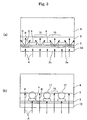
- the ultraviolet rays passing through a handle substrate 12 propagates straightforwardly through a gap 16 between the circuits 4 as indicated by arrows B, thereby curing the ultraviolet curable resin 5.
- the ultraviolet rays entering the circuits as indicated by arrows A cannot pass through the circuits, thus causing a shaded region 17 above each circuit.
- curing of the ultraviolet curable resin does not progress and the adhesion properties are maintained.
- curing of the resin progresses, whereby the resin loses its adhesion properties. If the composite substrate is intended to be removed from the supporting body in this state, it is easily removed over the region above each gap 16.
- the translucent polycrystalline alumina forming the handle substrate is set to have an average of the total forward light transmittance of 60% or higher in a wavelength range of 200 to 400 nm.
- the ultraviolet rays are effectively irradiated to the resin 5 as indicated by the arrows B.
- the linear light transmittance is lowered to 15% or lower, thereby scattering the ultraviolet rays within the handle substrate as indicated by arrows C.
- the donor substrate 3 is thin, the ultraviolet rays scattered in the handle substrate are effectively irradiated to regions above the circuits 4, which makes it difficult to generate the shaded regions.
- the resin 5 after irradiation with the ultraviolet rays is uniformly cured, which can prevent the occurrence of cracks or failure of removal in the composite substrate upon removing the composite substrate from the supporting body.
- a composite substrate of the invention can be used for light emitting elements for projectors, high-frequency devices, high-performance lasers, power devices, logic ICs, etc.
- the composite substrate includes a handle substrate according to the invention and a donor substrate.
- Examples of materials for the donor substrate include, but not limited thereto, preferably, one selected from the group consisting of silicon, aluminum nitride, gallium nitride, zinc oxide and diamond.
- the thickness of the donor substrate is not specifically limited, but is preferably in accordance with or close to the normal SEMI/JEITA specifications in terms of easiness of handling.
- the donor substrate contains the above-mentioned material, and may have an oxide film on its surface. This is because ion implantation through the oxide film can exhibit the effect of suppressing channeling of the implanted ions.
- the oxide film preferably has a thickness of 50 to 500 nm.
- the donor substrate with the oxide film may be implied in the term "donor substrate” as used herein and will be referred to as the "donor substrate” unless otherwise specified.
- the thickness of the handle substrate is not specifically limited, but is preferably in accordance with or close to the normal SEMI/JEITA specifications in terms of easiness of handling. Specifically, the thickness of the handle substrate is preferably, 525 ⁇ m for the wafer having a diameter of 100 mm; 625 ⁇ m for that of a diameter of 150 mm; 725 ⁇ m for that of a diameter of 200 mm; and 775 ⁇ m for that of a diameter of 300 mm.
- the handle substrate may also include a cavity.
- the material of the handle substrate is the translucent polycrystalline alumina described above.
- the translucent polycrystalline alumina has an average of the total forward light transmittance of 60% or higher in a wavelength range of 200 to 400 nm. With this arrangement, the amount of ultraviolet rays irradiated to the ultraviolet curable resin can be increased.
- the translucent polycrystalline alumina further preferably has an average of the total forward light transmittance of 65% or higher in the wavelength range of 200 to 400 nm.
- the translucent polycrystalline alumina forming the handle substrate has an average of the linear light transmittance of 15% or lower in the wavelength range of 200 to 400 nm.
- the translucent polycrystalline alumina further preferably has an average of the linear light transmittance of 10% or lower in the wavelength range of 200 to 400 nm.
- the total forward light transmittance is calculated based on a measurement value obtained by a measurement device 40 shown in Fig. 4 .
- a measurement device 40 shown in Fig. 4 an opening of an integrating sphere 41 is covered with a specimen S (of 1 mm in thickness), and a plate 42 with a hole 44 (of ⁇ 3 mm in diameter) is placed on the upper surface of the specimen S.
- the specimen S is irradiated with light from a light source 46 through the hole 44.
- the light passing through the specimen S is collected by use of the integrating sphere 41, thereby measuring the intensity of the light with a detector 48.
- the total forward light transmittance is determined by the following formula.
- the total forward light transmittance 100 ⁇ measured intensity of light / intensity of light from light source .
- the linear light transmittance is a value determined as follows.
- the linear light transmittance is measured in the same way as the total forward light transmittance.
- a distance between the specimen S and the integrating sphere 41 is set to 80 mm, and the dimension of the opening of the integrating sphere 41 is set to ⁇ 10 mm. Only the light passing through the opening straightforwardly from the specimen S is collected to measure the light intensity.
- ultraviolet ray means a ray having a wavelength of 200 nm or higher and 400 nm or lower.
- An alumina purity of the translucent polycrystalline alumina is 99.9% or higher.
- a relative density of the translucent polycrystalline alumina is preferably set to 98% or more, and more preferably to 99% or more, in terms of durability and contamination prevention during the post-processing of the semiconductor.
- An average crystal grain size of the translucent polycrystalline alumina is preferably in a range of 5 to 60 ⁇ m, thereby easily ensuring the smoothness of the bonding surface.
- the average crystal grain size of the translucent polycrystalline alumina is further preferably in a range of 10 to 50 ⁇ m.
- FIG. 6 An example of calculation of the average grain size is shown in FIG. 6 .
- a method for molding the handle substrate is not specifically limited, and may be any method including a doctor blade method, an extrusion process, a gel cast molding method, and the like.
- the substrate is manufactured by doctor blade method.
- a slurry containing ceramic powder, a dispersion medium and a bonding agent is molded in the form of a tape by doctor blade method. The tape is cut out into pieces, each having a predetermined shape. These pieces are laminated and pressurized into a molded body, and then the molded body is sintered.
- magnesium oxide powder 100 ppm or more and 300 ppm or less of magnesium oxide powder is preferably added to high-purity alumina powder having a purity of 99.9% or higher (more preferably, 99.95% or higher).
- high-purity alumina powder the high-purity alumina powder manufactured by Taimei Chemicals Co., Ltd. can be exemplified.
- the magnesium oxide powder may preferably have a purity of 99.9% or higher and an average grain size of 0.3 ⁇ m or smaller, respectively.
- An average particle size (primary particle size) of a raw material powder is not specifically limited, but preferably, 0.6 ⁇ m or less, and more preferably, 0.4 ⁇ m or less, in terms of densification in sintering at low temperature.
- the average particle size of the raw material powder is most preferably 0.3 ⁇ m or less.
- the lower limit of the average particle size is not specifically limited.
- the average particle size of the raw material powder can be determined by direct observation of the raw material powder using a scanning electron microscope (SEM).
- the doctor blade method can be performed, for example, in the following way.
- the sintering temperature is preferably in a range of 1700 to 1900°C, and more preferably in a range of 1750 to 1850°C in terms of densification of the sintered body. Further, a rate of temperature elevation at a temperature of 1400 to 1600°C is preferably set to 50 to 150°C/hr.
- the annealing temperature is preferably within the maximum temperature in the sintering ⁇ 100°C, in which the maximum temperature is more preferably 1900°C or lower, from the viewpoint of promoting discharge of magnesia, while preventing the deformation of the substrate and the occurrence of abnormal crystal grain growth.
- the annealing time period is preferably in a range of 1 to 6 hours.
- the annealing temperature is preferably set in a range of the maximum temperature in sintering + 0 to 100°C.
- the molding and the sintering are carried out to produce a blank substrate made of an alumina sintered body.
- the blank substrate is subjected to high-precision polishing to thereby decrease a microscopic center-line average surface roughness Ra of the surface of each crystal grain.
- a polishing process is, for example, a chemical mechanical polishing (CMP).
- CMP chemical mechanical polishing
- a polishing slurry suitable for use in this process is one obtained by dispersing abrasive grains having a grain diameter of 30 nm to 200 nm into alkali or neutral solution.
- materials for the abrasive grains can include silica, alumina, diamond, zirconia, and ceria. They are used either alone or in combination.
- the polishing pads can include a rigid urethane pad, a non-woven pad and a suede pad.
- Annealing treatment is desirably performed after executing a rough polishing process and before the final high-precision polishing process.
- Atmosphere gases suitable for the annealing treatment can include, for example, air, hydrogen, nitrogen, argon, and vacuum.
- the annealing temperature is preferably in a range of 1200 to 1600°C, and the annealing time period is preferably in a range of 2 to 12 hours.
- the discharge of magnesia can promote without degrading the smoothness of the surface.
- the microscopic center-line average surface roughness Ra of the surface of the handle substrate is 5 nm or less. If the surface roughness is large, the bonding strength of the donor substrate is decreased due to an intermolecular force.
- the center-line average surface roughness is more preferably 3 nm or less, and most preferably 1 nm or less. This is a value obtained by taking an image of an exposed surface of each crystal grain appearing at the surface of the specimen by an atomic force microscope, and by performing calculation according to JISB0601.
- the atomic force microscope is used to observe the surface morphology with a field of view of 10 ⁇ m when microscopically observing the surface roughness of each crystal grain surface.
- Techniques suitable for use in bonding of the handle substrate and the donor substrate include, but not limited to, for example, direct bonding by means of surface activation, and a substrate bonding technique using an adhesive layer.
- a low-temperature bonding technique through surface activation is suitably used.
- a monocrystalline material such as Si
- an adhesive layer such as SiO 2
- suitable materials for the adhesive layer can include SiO 2 , Al 2 O 3 , and SiN, in addition to resin for the adhesion.
- a circuit on the donor substrate can be formed by conventional photolithography and the like.
- the circuit includes various electronic elements, which includes solder bumps, printed electrodes, etc., in addition to fine wires made of noble metal.
- Suitable materials for the supporting body 6 can include silicon, a glass, quarts, and various kinds of ceramics, including alumina, SiC, zirconia, aluminum nitride, and the like.
- silicon and a glass are preferable in terms of the easiness of planarizing, thermal expansion matching, and cost.
- the supporting body may be provided with a number of through holes extending in the thickness direction.
- parts of the ultraviolet curable resin can enter the through holes to strength the bonding, and a removal solution can be supplied from the through holes in removal of the supporting body.
- the ultraviolet curable resin can have the composition that includes (i) an adhesive (polymeric elastomer), such as an acrylic adhesive or a saturated copolyester, (ii) an ultraviolet curable component, (iii) a photopolymerization initiator, and optionally, conventional additives, including a cross-linker, a tackifier, a plasticizer, a filler, an antioxidant, a coloring agent, etc.
- an adhesive polymeric elastomer
- an ultraviolet curable component such as an acrylic adhesive or a saturated copolyester
- a photopolymerization initiator such as an acrylic adhesive or a saturated copolyester
- conventional additives including a cross-linker, a tackifier, a plasticizer, a filler, an antioxidant, a coloring agent, etc.
- the acrylic adhesive that is normally used is a homopolymer of a (meth)acrylic acid ester, or a copolymer of the (meth)acrylic acid ester with a copolymeric comonomer.
- Suitable monomers or comonomers configuring these polymers can include, for example, alkyl esters of (meth)acrylic acid (e.g., methyl ester, ethyl ester, butyl ester, 2-ethylhexyl ester, octyl ester, etc.), hydroxyalkyl esters of (meth)acrylic acid (e.g., hydroxyethyl ester, hydroxypropyl ester), (meth)acrylic acid glycidyl ester, (meth)acrylic acid, itaconic acid, maleic anhydride, (meth)acrylic acid amides, (meth)acrylic acid N-hydroxymethyl amide, (meth)acrylic acid alkyl aminoalkyl ester (for example, dimethylaminoethyl methacrylate, t-butylaminoethyl methacrylate, etc.), vinyl acetate, styrene, acrylonitrile,
- saturated copolyesters of a polyhydric alcohol with 2 or more kinds of polycarboxylic acids can be exemplified.
- the polyhydric alcohols can include glycols, such as ethylene glycol, propylene glycol, and 1,4-butanediol.
- the polycarboxylic acid can include aromatic dicarboxylic acids, such as terephthalic acid and isophthalic acid; and aliphatic dicarboxylic acids, such as adipic acid and sebacic acid.
- the polycarboxylic acid a combination of the aromatic dicarboxylic acid and aliphatic dicarboxylic acid is used in many cases.
- the ultraviolet curable component may be any monomer, oligomer, polymer and the like that have a carbon-carbon double bond in a molecule and are curable by radical polymerization.
- the ultraviolet curable component can include esters of (meth)acrylic acid with a polyhydric alcohol, such as trimethylolpropane tri(meth)acrylate, pentaerythritol tri(meth)acrylate, tetraethylene glycol di(meth)acrylate, 1,6-hexanediol di(meth)acrylate, neopentyl glycol di(meth)acrylate, and dipentaerythritol hexa(meth)acrylate; ester acrylate oligomers; cyanurate or isocyanurate compounds, such as 2-propenyl di-3-butenyl cyanurate, 2-hydroxyethyl bis(2-acryloxyethyl) isocyanurate, tris(2-acryloxyethyl
- the polymerization initiator may be any substance that is cleaved by irradiation with ultraviolet rays having an appropriate wavelength, which can trigger a polymerization reaction to generate radicals.
- the polymerization initiator can include benzoin alkyl ethers, such as benzoin methyl ether, benzoin isopropyl ether, and benzoin isobutyl ether; aromatic ketones, such as benzyl, benzoin, benzophenone, ⁇ -hydroxycyclohexyl phenyl ketone; aromatic ketals, such as benzyl dimethyl ketal; polyvinyl benzophenone; and thioxanthones, such as chlorothioxanthone, dodecyl thioxanthone, dimethyl thioxanthone, and diethyl thioxanthone.
- Suitable cross-linkers can include, for example, a polyisocyanate compound, a melamine resin, a urea resin, an epoxy resin, an acid anhydride, a polyamine, and a carboxy group containing polymer.
- the slurry was molded in the form of tape by doctor blade method so that the thickness after the sintering becomes 0.25 mm.
- Four tape-shaped molded bodies were laminated in layers and pressed, thereby producing a substrate-shaped powder molded body so as to have a thickness of 1 mm after the sintering.
- the powder molded body obtained in this way was calcined (subjected to preliminary sintering) at 1100°C in air. Then, the substrate was placed on a plate made of molybdenum and sintered at 1750°C by increasing the temperature from 1400°C to 1600°C at a rate of temperature elevation of 50°C/h, in atmosphere containing hydrogen and nitrogen mixed at 3:1, with a space of 0.1 to 0.5 mm maintained over the upper side, in order to sufficiently discharge pores from the grain boundaries. Thereafter, the sintered substrate was placed on a plate made of molybdenum and subjected to an annealing treatment at 1750°C for three hours by placing a molybdenum weight on the substrate.
- the substrate obtained in this manner had an outer diameter of ⁇ 4 inches, a thickness of 1 mm.
- An average grain size at the surface of was 20 ⁇ m, and a porosity was 0.1% or less by observation of its section.
- the space was formed over the upper side, thereby enabling discharge of the additive (mainly magnesia or the like), and the annealing treatment was performed at the substantially same temperature as that in the sintering with the weight placed on (a load applied to) the substrate, thereby allowing for acceleration of the discharge of pores.
- the additive mainly magnesia or the like
- an average of the total forward light transmittance was 60%, and an average of the linear light transmittance was 15%, in a wavelength range of 200 to 400 nm.
- An alumina purity of the translucent polycrystalline alumina forming the handle substrate was 99.9%.
- the substrate was polished to a thickness of 0.6 mm by using green carbon (GC) abrasive grains, diamond abrasive grains and a CMP liquid in this order, thereby producing the substrate 2.
- GC green carbon
- a monocrystalline Si substrate with ⁇ 4 inches in diameter and 250 ⁇ m in thickness was prepared. Then, the monocrystalline Si substrate and the above-mentioned substrate 2 were directly bonded together by plasma activation. Both substrates used for bonding were subjected to a plasma treatment with nitrogen, and then washed with water to remove particles on their surfaces. Both these substrates have their ends pressed to be in intimate contact with each other. The pressed parts of the substrates were bonded together, whereby the bonding was transferred across their whole surfaces. This phenomenon is that the bonding between the substrates automatically progresses through a force (surface-surface attractive force) by which both the substrates are attracted to each other, which can be observed when the surface of the substrate is polished to be very smooth.
- a force surface-surface attractive force
- the monocrystalline Si substrate side was ground by a grinder to a thickness of 20 ⁇ m, and then was subjected to lapping using diamond abrasive grains having a grain size of 1 ⁇ m and a surface plate of tin until its thickness was 3 ⁇ m.
- the substrate was polished using colloidal silica and an urethane pad to a thickness of 0.2 ⁇ m.
- the annealing treatment was performed on the Si substrate at 300°C, thereby producing a composite substrate including the substrate 2 and the donor substrate 3.
- the monocrystalline Si substrate was bonded as the supporting body 6 to the main surface on the circuit 4 side of the semiconductor circuit board obtained in this way, via the ultraviolet curable resin.
- the backside 2b of the semiconductor circuit board was ground by the grinder until the thickness of the semiconductor circuit board was 120 ⁇ m. Thereafter, dicing grooves 9 were formed so as to produce the plurality of composite substrates each having a size of 1 mm x 1 mm, depending on the formed circuits 4.
- ultraviolet rays having a central wavelength of 365 nm were applied at 300 mJ/cm 2 from the side of the handle substrate 2A to cure the ultraviolet curable resin 5.
- 100 pieces of semiconductor circuit boards 10 were removed thereby from the supporting body 6, and one piece of substrate 10 was observed to have a crack or a failure of removal.
- Example 2 In the same way as Example 1, the composite substrate was fabricated. Note that as a result of the measurements, in the translucent alumina substrate obtained in this way, an average of the total forward light transmittance was 65%, and an average of the linear light transmittance was 10%, in a wavelength range of 200 to 400 nm. An alumina purity of the translucent polycrystalline alumina forming the handle substrate was 99.9%.
- the sintering temperature was changed to 1710°C
- the annealing temperature and time was changed to 1710°C x 12 hr.
- ultraviolet rays having a central wavelength of 365 nm were applied at 300 mJ/cm 2 from the side of the handle substrate 2A to cure the ultraviolet curable resin 5.
- 100 pieces of semiconductor circuit boards 10 were thereby removed from the supporting body 6, no substrate 10 with cracks and failures of removal was observed.
- Example 2 In the same way as Example 1, a semiconductor circuit board and a supporting body were bonded together with an ultraviolet curable resin, and the ultraviolet curable resin was cured. 100 pieces of the semiconductor circuit boards 10 were thereby removed from the supporting body.
- the handle substrate was made of monocrystalline sapphire, and had an average of the total forward light transmittance of 85% as well as an average of the linear light transmittance of 80%, in a wavelength range of 200 to 400 nm.
- ultraviolet rays having a central wavelength of 365 nm were applied at 300 mJ/cm 2 to cure the ultraviolet curable resin 5 from the side of the handle substrate 2A.
- 100 pieces of semiconductor circuit boards 10 individually cut were thereby removed from the supporting body 6, nine substrates 10 were observed to have a crack or failure of removal.
- Example 2 In the same way as Example 1, a semiconductor circuit board and a supporting body were bonded together with an ultraviolet curable resin, and the ultraviolet curable resin was cured. 100 pieces of the semiconductor circuit boards 10 were thereby tried to be removed from the supporting body.
- the handle substrate was made of alumina (having a purity of 99.5%), and had an average of the total forward light transmittance of 50% as well as an average of the linear light transmittance of 1% or less, in a wavelength range of 200 to 400 nm.
- ultraviolet rays having a central wavelength of 365 nm were applied at 300 mJ/cm 2 from the side of the handle substrate 2A to the ultraviolet curable resin 5.
- the ultraviolet curable resin 5 was not cured, and thus the respective semiconductor circuit boards 10 individually cut failed to be removed from the supporting body 6.
Landscapes
- Chemical & Material Sciences (AREA)
- Engineering & Computer Science (AREA)
- Ceramic Engineering (AREA)
- Organic Chemistry (AREA)
- Materials Engineering (AREA)
- Manufacturing & Machinery (AREA)
- Structural Engineering (AREA)
- Inorganic Chemistry (AREA)
- Geology (AREA)
- Life Sciences & Earth Sciences (AREA)
- Adhesives Or Adhesive Processes (AREA)
- Crystallography & Structural Chemistry (AREA)
- Container, Conveyance, Adherence, Positioning, Of Wafer (AREA)
- Crystals, And After-Treatments Of Crystals (AREA)
- Polishing Bodies And Polishing Tools (AREA)
- Thin Film Transistor (AREA)
- Mechanical Treatment Of Semiconductor (AREA)
Applications Claiming Priority (2)
| Application Number | Priority Date | Filing Date | Title |
|---|---|---|---|
| JP2013267455 | 2013-12-25 | ||
| PCT/JP2014/083209 WO2015098609A1 (ja) | 2013-12-25 | 2014-12-16 | ハンドル基板、半導体用複合基板、半導体回路基板およびその製造方法 |
Publications (3)
| Publication Number | Publication Date |
|---|---|
| EP2978009A1 true EP2978009A1 (de) | 2016-01-27 |
| EP2978009A4 EP2978009A4 (de) | 2016-12-28 |
| EP2978009B1 EP2978009B1 (de) | 2018-03-21 |
Family
ID=53478473
Family Applications (1)
| Application Number | Title | Priority Date | Filing Date |
|---|---|---|---|
| EP14873693.7A Not-in-force EP2978009B1 (de) | 2013-12-25 | 2014-12-16 | Griffsubstrat, verbundsubstrat für halbleiter und halbleiterschaltungsplatte und verfahren zur herstellung davon |
Country Status (7)
| Country | Link |
|---|---|
| US (1) | US9425083B2 (de) |
| EP (1) | EP2978009B1 (de) |
| JP (1) | JP5781254B1 (de) |
| KR (1) | KR101570958B1 (de) |
| CN (1) | CN105074870B (de) |
| TW (1) | TWI514441B (de) |
| WO (1) | WO2015098609A1 (de) |
Cited By (2)
| Publication number | Priority date | Publication date | Assignee | Title |
|---|---|---|---|---|
| EP3010051A4 (de) * | 2013-06-12 | 2017-02-22 | NGK Insulators, Ltd. | Fenstermaterial für element zur emittierung ultravioletter strahlen und verfahren zur herstellung davon |
| EP3113211A4 (de) * | 2014-02-26 | 2017-10-11 | NGK Insulators, Ltd. | Handhabung eines substrats für ein verbundsubstrat für einen halbleiter |
Families Citing this family (7)
| Publication number | Priority date | Publication date | Assignee | Title |
|---|---|---|---|---|
| EP3221882A4 (de) * | 2015-07-14 | 2018-05-02 | Goertek Inc. | Montageverfahren, herstellungsverfahren, vorrichtung und elektronische vorrichtung einer flip-matrize |
| US10446442B2 (en) | 2016-12-21 | 2019-10-15 | Globalfoundries Inc. | Integrated circuit chip with molding compound handler substrate and method |
| JP6980421B2 (ja) * | 2017-06-16 | 2021-12-15 | 株式会社ディスコ | ウエーハの加工方法 |
| CN113544819B (zh) * | 2019-03-22 | 2024-01-05 | 日本碍子株式会社 | 预固定基板、复合基板以及电子元件的剥离方法 |
| JP2025086064A (ja) * | 2023-11-27 | 2025-06-06 | タツモ株式会社 | 半導体デバイスの製造方法 |
| JP2025086063A (ja) * | 2023-11-27 | 2025-06-06 | タツモ株式会社 | 半導体デバイスの製造方法 |
| CN118573145B (zh) * | 2024-08-01 | 2024-12-20 | 泉州市三安集成电路有限公司 | 支撑基板及其制备方法、复合基板、电子器件和模块 |
Family Cites Families (24)
| Publication number | Priority date | Publication date | Assignee | Title |
|---|---|---|---|---|
| JP3323945B2 (ja) | 1991-12-03 | 2002-09-09 | 東芝セラミックス株式会社 | ダミーウェーハ |
| EP0567095B1 (de) * | 1992-04-22 | 1996-07-03 | Sumitomo Chemical Company, Limited | Polykristalliner, lichtdurchlässiger Aluminiumoxidkörper und Verfahren zu seiner Herstellung |
| US5572040A (en) | 1993-07-12 | 1996-11-05 | Peregrine Semiconductor Corporation | High-frequency wireless communication system on a single ultrathin silicon on sapphire chip |
| US5864162A (en) | 1993-07-12 | 1999-01-26 | Peregrine Seimconductor Corporation | Apparatus and method of making a self-aligned integrated resistor load on ultrathin silicon on sapphire |
| US5587346A (en) * | 1995-06-16 | 1996-12-24 | Osram Sylvania, Inc. | Translucent polycrystalline alumina |
| JP3783445B2 (ja) * | 1999-01-29 | 2006-06-07 | 住友化学株式会社 | 透光性アルミナ焼結体の製造方法およびその用途 |
| CA2308933C (en) * | 1999-05-19 | 2008-07-22 | Ngk Spark Plug Co., Ltd. | Translucent polycrystalline ceramic and method for making same |
| FR2834123B1 (fr) | 2001-12-21 | 2005-02-04 | Soitec Silicon On Insulator | Procede de report de couches minces semi-conductrices et procede d'obtention d'une plaquette donneuse pour un tel procede de report |
| US6878456B2 (en) * | 2001-12-28 | 2005-04-12 | 3M Innovative Properties Co. | Polycrystalline translucent alumina-based ceramic material, uses, and methods |
| JP4405246B2 (ja) * | 2003-11-27 | 2010-01-27 | スリーエム イノベイティブ プロパティズ カンパニー | 半導体チップの製造方法 |
| JP2005191550A (ja) | 2003-12-01 | 2005-07-14 | Tokyo Ohka Kogyo Co Ltd | 基板の貼り付け方法 |
| CN100420651C (zh) * | 2005-11-03 | 2008-09-24 | 韩敏芳 | 具有高线性透光率的亚微米晶粒透明氧化铝陶瓷 |
| JP5274859B2 (ja) | 2007-04-18 | 2013-08-28 | 信越化学工業株式会社 | 貼り合わせ基板の製造方法 |
| US8088670B2 (en) | 2007-04-18 | 2012-01-03 | Shin-Etsu Chemical Co., Ltd. | Method for manufacturing bonded substrate with sandblast treatment |
| JP5290853B2 (ja) | 2009-04-28 | 2013-09-18 | 三菱樹脂株式会社 | ダイシング用粘着シート |
| JP5420968B2 (ja) | 2009-05-07 | 2014-02-19 | 信越化学工業株式会社 | 貼り合わせウェーハの製造方法 |
| JP2010278341A (ja) | 2009-05-29 | 2010-12-09 | Shin-Etsu Chemical Co Ltd | 貼り合わせsos基板 |
| KR101694112B1 (ko) * | 2012-06-13 | 2017-01-06 | 엔지케이 인슐레이터 엘티디 | 복합 기판 |
| JP5491680B1 (ja) * | 2012-07-18 | 2014-05-14 | 日本碍子株式会社 | 複合ウェハー及びその製法 |
| CN102992739A (zh) * | 2012-12-17 | 2013-03-27 | 江苏大学 | 一种多功能透明氧化铝陶瓷的制备方法 |
| TWI629753B (zh) * | 2013-04-26 | 2018-07-11 | Ngk Insulators, Ltd. | 半導體用複合基板之操作基板 |
| WO2015008694A1 (ja) * | 2013-07-18 | 2015-01-22 | 日本碍子株式会社 | 半導体用複合基板のハンドル基板 |
| CN105051862B (zh) * | 2014-01-06 | 2016-11-09 | 日本碍子株式会社 | 支撑基板以及半导体用复合晶片 |
| KR102263959B1 (ko) * | 2014-02-26 | 2021-06-11 | 엔지케이 인슐레이터 엘티디 | 반도체용 복합 기판의 핸들 기판 |
-
2014
- 2014-12-16 JP JP2015518488A patent/JP5781254B1/ja not_active Expired - Fee Related
- 2014-12-16 KR KR1020157021527A patent/KR101570958B1/ko not_active Expired - Fee Related
- 2014-12-16 EP EP14873693.7A patent/EP2978009B1/de not_active Not-in-force
- 2014-12-16 CN CN201480019693.7A patent/CN105074870B/zh not_active Expired - Fee Related
- 2014-12-16 WO PCT/JP2014/083209 patent/WO2015098609A1/ja not_active Ceased
- 2014-12-22 TW TW103144719A patent/TWI514441B/zh not_active IP Right Cessation
-
2015
- 2015-09-14 US US14/853,011 patent/US9425083B2/en not_active Expired - Fee Related
Cited By (2)
| Publication number | Priority date | Publication date | Assignee | Title |
|---|---|---|---|---|
| EP3010051A4 (de) * | 2013-06-12 | 2017-02-22 | NGK Insulators, Ltd. | Fenstermaterial für element zur emittierung ultravioletter strahlen und verfahren zur herstellung davon |
| EP3113211A4 (de) * | 2014-02-26 | 2017-10-11 | NGK Insulators, Ltd. | Handhabung eines substrats für ein verbundsubstrat für einen halbleiter |
Also Published As
| Publication number | Publication date |
|---|---|
| TWI514441B (zh) | 2015-12-21 |
| WO2015098609A1 (ja) | 2015-07-02 |
| CN105074870B (zh) | 2016-12-07 |
| JPWO2015098609A1 (ja) | 2017-03-23 |
| EP2978009B1 (de) | 2018-03-21 |
| US9425083B2 (en) | 2016-08-23 |
| TW201537617A (zh) | 2015-10-01 |
| CN105074870A (zh) | 2015-11-18 |
| KR20150097812A (ko) | 2015-08-26 |
| KR101570958B1 (ko) | 2015-11-20 |
| US20160005643A1 (en) | 2016-01-07 |
| EP2978009A4 (de) | 2016-12-28 |
| JP5781254B1 (ja) | 2015-09-16 |
Similar Documents
| Publication | Publication Date | Title |
|---|---|---|
| EP2978009B1 (de) | Griffsubstrat, verbundsubstrat für halbleiter und halbleiterschaltungsplatte und verfahren zur herstellung davon | |
| KR102222089B1 (ko) | 복합 기판, 반도체 디바이스 및 반도체 디바이스의 제법 | |
| KR101597501B1 (ko) | 핸들 기판 및 반도체용 복합 웨이퍼 | |
| EP3113211B1 (de) | Griffsubstrat für verbundsubstrat für halbleiter und verbundsubstrat für halbleiter | |
| KR101595693B1 (ko) | 반도체용 복합 기판의 핸들 기판 | |
| KR102188440B1 (ko) | 반도체용 복합 기판의 핸들 기판 | |
| US9538653B2 (en) | Insulating substrates including through holes | |
| JP5697813B1 (ja) | 半導体用複合基板のハンドル基板 | |
| KR101642671B1 (ko) | 반도체용 복합 기판의 핸들 기판 및 반도체용 복합 기판 | |
| US20200027755A1 (en) | Temporary-fixing substrate and method for molding electronic component |
Legal Events
| Date | Code | Title | Description |
|---|---|---|---|
| PUAI | Public reference made under article 153(3) epc to a published international application that has entered the european phase |
Free format text: ORIGINAL CODE: 0009012 |
|
| 17P | Request for examination filed |
Effective date: 20150924 |
|
| AK | Designated contracting states |
Kind code of ref document: A1 Designated state(s): AL AT BE BG CH CY CZ DE DK EE ES FI FR GB GR HR HU IE IS IT LI LT LU LV MC MK MT NL NO PL PT RO RS SE SI SK SM TR |
|
| AX | Request for extension of the european patent |
Extension state: BA ME |
|
| RIC1 | Information provided on ipc code assigned before grant |
Ipc: C04B 35/115 20060101ALI20161116BHEP Ipc: H01L 29/06 20060101ALI20161116BHEP Ipc: H01L 27/12 20060101ALI20161116BHEP Ipc: H01L 21/762 20060101ALI20161116BHEP Ipc: C04B 37/00 20060101ALI20161116BHEP Ipc: H01L 23/15 20060101ALI20161116BHEP Ipc: C04B 35/64 20060101ALI20161116BHEP Ipc: H01L 21/683 20060101ALI20161116BHEP Ipc: H01L 21/02 20060101AFI20161116BHEP Ipc: C01F 7/02 20060101ALI20161116BHEP |
|
| A4 | Supplementary search report drawn up and despatched |
Effective date: 20161125 |
|
| DAX | Request for extension of the european patent (deleted) | ||
| GRAP | Despatch of communication of intention to grant a patent |
Free format text: ORIGINAL CODE: EPIDOSNIGR1 |
|
| INTG | Intention to grant announced |
Effective date: 20171006 |
|
| GRAS | Grant fee paid |
Free format text: ORIGINAL CODE: EPIDOSNIGR3 |
|
| GRAA | (expected) grant |
Free format text: ORIGINAL CODE: 0009210 |
|
| AK | Designated contracting states |
Kind code of ref document: B1 Designated state(s): AL AT BE BG CH CY CZ DE DK EE ES FI FR GB GR HR HU IE IS IT LI LT LU LV MC MK MT NL NO PL PT RO RS SE SI SK SM TR |
|
| REG | Reference to a national code |
Ref country code: GB Ref legal event code: FG4D |
|
| REG | Reference to a national code |
Ref country code: CH Ref legal event code: EP |
|
| REG | Reference to a national code |
Ref country code: AT Ref legal event code: REF Ref document number: 981942 Country of ref document: AT Kind code of ref document: T Effective date: 20180415 |
|
| REG | Reference to a national code |
Ref country code: IE Ref legal event code: FG4D |
|
| REG | Reference to a national code |
Ref country code: DE Ref legal event code: R096 Ref document number: 602014022834 Country of ref document: DE |
|
| REG | Reference to a national code |
Ref country code: NL Ref legal event code: MP Effective date: 20180321 |
|
| PG25 | Lapsed in a contracting state [announced via postgrant information from national office to epo] |
Ref country code: LT Free format text: LAPSE BECAUSE OF FAILURE TO SUBMIT A TRANSLATION OF THE DESCRIPTION OR TO PAY THE FEE WITHIN THE PRESCRIBED TIME-LIMIT Effective date: 20180321 Ref country code: HR Free format text: LAPSE BECAUSE OF FAILURE TO SUBMIT A TRANSLATION OF THE DESCRIPTION OR TO PAY THE FEE WITHIN THE PRESCRIBED TIME-LIMIT Effective date: 20180321 Ref country code: NO Free format text: LAPSE BECAUSE OF FAILURE TO SUBMIT A TRANSLATION OF THE DESCRIPTION OR TO PAY THE FEE WITHIN THE PRESCRIBED TIME-LIMIT Effective date: 20180621 Ref country code: CY Free format text: LAPSE BECAUSE OF FAILURE TO SUBMIT A TRANSLATION OF THE DESCRIPTION OR TO PAY THE FEE WITHIN THE PRESCRIBED TIME-LIMIT Effective date: 20180321 Ref country code: FI Free format text: LAPSE BECAUSE OF FAILURE TO SUBMIT A TRANSLATION OF THE DESCRIPTION OR TO PAY THE FEE WITHIN THE PRESCRIBED TIME-LIMIT Effective date: 20180321 |
|
| REG | Reference to a national code |
Ref country code: LT Ref legal event code: MG4D |
|
| REG | Reference to a national code |
Ref country code: AT Ref legal event code: MK05 Ref document number: 981942 Country of ref document: AT Kind code of ref document: T Effective date: 20180321 |
|
| PG25 | Lapsed in a contracting state [announced via postgrant information from national office to epo] |
Ref country code: LV Free format text: LAPSE BECAUSE OF FAILURE TO SUBMIT A TRANSLATION OF THE DESCRIPTION OR TO PAY THE FEE WITHIN THE PRESCRIBED TIME-LIMIT Effective date: 20180321 Ref country code: SE Free format text: LAPSE BECAUSE OF FAILURE TO SUBMIT A TRANSLATION OF THE DESCRIPTION OR TO PAY THE FEE WITHIN THE PRESCRIBED TIME-LIMIT Effective date: 20180321 Ref country code: GR Free format text: LAPSE BECAUSE OF FAILURE TO SUBMIT A TRANSLATION OF THE DESCRIPTION OR TO PAY THE FEE WITHIN THE PRESCRIBED TIME-LIMIT Effective date: 20180622 Ref country code: RS Free format text: LAPSE BECAUSE OF FAILURE TO SUBMIT A TRANSLATION OF THE DESCRIPTION OR TO PAY THE FEE WITHIN THE PRESCRIBED TIME-LIMIT Effective date: 20180321 Ref country code: BG Free format text: LAPSE BECAUSE OF FAILURE TO SUBMIT A TRANSLATION OF THE DESCRIPTION OR TO PAY THE FEE WITHIN THE PRESCRIBED TIME-LIMIT Effective date: 20180621 |
|
| PG25 | Lapsed in a contracting state [announced via postgrant information from national office to epo] |
Ref country code: IT Free format text: LAPSE BECAUSE OF FAILURE TO SUBMIT A TRANSLATION OF THE DESCRIPTION OR TO PAY THE FEE WITHIN THE PRESCRIBED TIME-LIMIT Effective date: 20180321 Ref country code: AL Free format text: LAPSE BECAUSE OF FAILURE TO SUBMIT A TRANSLATION OF THE DESCRIPTION OR TO PAY THE FEE WITHIN THE PRESCRIBED TIME-LIMIT Effective date: 20180321 Ref country code: EE Free format text: LAPSE BECAUSE OF FAILURE TO SUBMIT A TRANSLATION OF THE DESCRIPTION OR TO PAY THE FEE WITHIN THE PRESCRIBED TIME-LIMIT Effective date: 20180321 Ref country code: PL Free format text: LAPSE BECAUSE OF FAILURE TO SUBMIT A TRANSLATION OF THE DESCRIPTION OR TO PAY THE FEE WITHIN THE PRESCRIBED TIME-LIMIT Effective date: 20180321 Ref country code: NL Free format text: LAPSE BECAUSE OF FAILURE TO SUBMIT A TRANSLATION OF THE DESCRIPTION OR TO PAY THE FEE WITHIN THE PRESCRIBED TIME-LIMIT Effective date: 20180321 Ref country code: ES Free format text: LAPSE BECAUSE OF FAILURE TO SUBMIT A TRANSLATION OF THE DESCRIPTION OR TO PAY THE FEE WITHIN THE PRESCRIBED TIME-LIMIT Effective date: 20180321 Ref country code: RO Free format text: LAPSE BECAUSE OF FAILURE TO SUBMIT A TRANSLATION OF THE DESCRIPTION OR TO PAY THE FEE WITHIN THE PRESCRIBED TIME-LIMIT Effective date: 20180321 |
|
| PG25 | Lapsed in a contracting state [announced via postgrant information from national office to epo] |
Ref country code: SM Free format text: LAPSE BECAUSE OF FAILURE TO SUBMIT A TRANSLATION OF THE DESCRIPTION OR TO PAY THE FEE WITHIN THE PRESCRIBED TIME-LIMIT Effective date: 20180321 Ref country code: AT Free format text: LAPSE BECAUSE OF FAILURE TO SUBMIT A TRANSLATION OF THE DESCRIPTION OR TO PAY THE FEE WITHIN THE PRESCRIBED TIME-LIMIT Effective date: 20180321 Ref country code: CZ Free format text: LAPSE BECAUSE OF FAILURE TO SUBMIT A TRANSLATION OF THE DESCRIPTION OR TO PAY THE FEE WITHIN THE PRESCRIBED TIME-LIMIT Effective date: 20180321 Ref country code: SK Free format text: LAPSE BECAUSE OF FAILURE TO SUBMIT A TRANSLATION OF THE DESCRIPTION OR TO PAY THE FEE WITHIN THE PRESCRIBED TIME-LIMIT Effective date: 20180321 |
|
| PG25 | Lapsed in a contracting state [announced via postgrant information from national office to epo] |
Ref country code: PT Free format text: LAPSE BECAUSE OF FAILURE TO SUBMIT A TRANSLATION OF THE DESCRIPTION OR TO PAY THE FEE WITHIN THE PRESCRIBED TIME-LIMIT Effective date: 20180723 |
|
| REG | Reference to a national code |
Ref country code: DE Ref legal event code: R097 Ref document number: 602014022834 Country of ref document: DE |
|
| PLBE | No opposition filed within time limit |
Free format text: ORIGINAL CODE: 0009261 |
|
| STAA | Information on the status of an ep patent application or granted ep patent |
Free format text: STATUS: NO OPPOSITION FILED WITHIN TIME LIMIT |
|
| PG25 | Lapsed in a contracting state [announced via postgrant information from national office to epo] |
Ref country code: DK Free format text: LAPSE BECAUSE OF FAILURE TO SUBMIT A TRANSLATION OF THE DESCRIPTION OR TO PAY THE FEE WITHIN THE PRESCRIBED TIME-LIMIT Effective date: 20180321 |
|
| 26N | No opposition filed |
Effective date: 20190102 |
|
| PG25 | Lapsed in a contracting state [announced via postgrant information from national office to epo] |
Ref country code: SI Free format text: LAPSE BECAUSE OF FAILURE TO SUBMIT A TRANSLATION OF THE DESCRIPTION OR TO PAY THE FEE WITHIN THE PRESCRIBED TIME-LIMIT Effective date: 20180321 |
|
| REG | Reference to a national code |
Ref country code: CH Ref legal event code: PL |
|
| GBPC | Gb: european patent ceased through non-payment of renewal fee |
Effective date: 20181216 |
|
| PG25 | Lapsed in a contracting state [announced via postgrant information from national office to epo] |
Ref country code: LU Free format text: LAPSE BECAUSE OF NON-PAYMENT OF DUE FEES Effective date: 20181216 Ref country code: MC Free format text: LAPSE BECAUSE OF FAILURE TO SUBMIT A TRANSLATION OF THE DESCRIPTION OR TO PAY THE FEE WITHIN THE PRESCRIBED TIME-LIMIT Effective date: 20180321 |
|
| REG | Reference to a national code |
Ref country code: IE Ref legal event code: MM4A |
|
| REG | Reference to a national code |
Ref country code: BE Ref legal event code: MM Effective date: 20181231 |
|
| PG25 | Lapsed in a contracting state [announced via postgrant information from national office to epo] |
Ref country code: IE Free format text: LAPSE BECAUSE OF NON-PAYMENT OF DUE FEES Effective date: 20181216 |
|
| PG25 | Lapsed in a contracting state [announced via postgrant information from national office to epo] |
Ref country code: BE Free format text: LAPSE BECAUSE OF NON-PAYMENT OF DUE FEES Effective date: 20181231 |
|
| PG25 | Lapsed in a contracting state [announced via postgrant information from national office to epo] |
Ref country code: LI Free format text: LAPSE BECAUSE OF NON-PAYMENT OF DUE FEES Effective date: 20181231 Ref country code: GB Free format text: LAPSE BECAUSE OF NON-PAYMENT OF DUE FEES Effective date: 20181216 Ref country code: CH Free format text: LAPSE BECAUSE OF NON-PAYMENT OF DUE FEES Effective date: 20181231 |
|
| PG25 | Lapsed in a contracting state [announced via postgrant information from national office to epo] |
Ref country code: MT Free format text: LAPSE BECAUSE OF NON-PAYMENT OF DUE FEES Effective date: 20181216 |
|
| PG25 | Lapsed in a contracting state [announced via postgrant information from national office to epo] |
Ref country code: TR Free format text: LAPSE BECAUSE OF FAILURE TO SUBMIT A TRANSLATION OF THE DESCRIPTION OR TO PAY THE FEE WITHIN THE PRESCRIBED TIME-LIMIT Effective date: 20180321 |
|
| PG25 | Lapsed in a contracting state [announced via postgrant information from national office to epo] |
Ref country code: HU Free format text: LAPSE BECAUSE OF FAILURE TO SUBMIT A TRANSLATION OF THE DESCRIPTION OR TO PAY THE FEE WITHIN THE PRESCRIBED TIME-LIMIT; INVALID AB INITIO Effective date: 20141216 Ref country code: MK Free format text: LAPSE BECAUSE OF NON-PAYMENT OF DUE FEES Effective date: 20180321 |
|
| PG25 | Lapsed in a contracting state [announced via postgrant information from national office to epo] |
Ref country code: IS Free format text: LAPSE BECAUSE OF FAILURE TO SUBMIT A TRANSLATION OF THE DESCRIPTION OR TO PAY THE FEE WITHIN THE PRESCRIBED TIME-LIMIT Effective date: 20180721 |
|
| PGFP | Annual fee paid to national office [announced via postgrant information from national office to epo] |
Ref country code: DE Payment date: 20201201 Year of fee payment: 7 Ref country code: FR Payment date: 20201112 Year of fee payment: 7 |
|
| REG | Reference to a national code |
Ref country code: DE Ref legal event code: R119 Ref document number: 602014022834 Country of ref document: DE |
|
| PG25 | Lapsed in a contracting state [announced via postgrant information from national office to epo] |
Ref country code: DE Free format text: LAPSE BECAUSE OF NON-PAYMENT OF DUE FEES Effective date: 20220701 |
|
| PG25 | Lapsed in a contracting state [announced via postgrant information from national office to epo] |
Ref country code: FR Free format text: LAPSE BECAUSE OF NON-PAYMENT OF DUE FEES Effective date: 20211231 |