EP2979100B1 - Dispositif et procédé avec un support présentant des structures de commutation - Google Patents
Dispositif et procédé avec un support présentant des structures de commutation Download PDFInfo
- Publication number
- EP2979100B1 EP2979100B1 EP14713050.4A EP14713050A EP2979100B1 EP 2979100 B1 EP2979100 B1 EP 2979100B1 EP 14713050 A EP14713050 A EP 14713050A EP 2979100 B1 EP2979100 B1 EP 2979100B1
- Authority
- EP
- European Patent Office
- Prior art keywords
- carrier
- circuit structures
- result
- component
- circuit
- Prior art date
- Legal status (The legal status is an assumption and is not a legal conclusion. Google has not performed a legal analysis and makes no representation as to the accuracy of the status listed.)
- Active
Links
Images



Classifications
-
- G—PHYSICS
- G06—COMPUTING OR CALCULATING; COUNTING
- G06F—ELECTRIC DIGITAL DATA PROCESSING
- G06F21/00—Security arrangements for protecting computers, components thereof, programs or data against unauthorised activity
- G06F21/50—Monitoring users, programs or devices to maintain the integrity of platforms, e.g. of processors, firmware or operating systems
- G06F21/55—Detecting local intrusion or implementing counter-measures
- G06F21/552—Detecting local intrusion or implementing counter-measures involving long-term monitoring or reporting
-
- G—PHYSICS
- G01—MEASURING; TESTING
- G01R—MEASURING ELECTRIC VARIABLES; MEASURING MAGNETIC VARIABLES
- G01R31/00—Arrangements for testing electric properties; Arrangements for locating electric faults; Arrangements for electrical testing characterised by what is being tested not provided for elsewhere
- G01R31/28—Testing of electronic circuits, e.g. by signal tracer
-
- G—PHYSICS
- G06—COMPUTING OR CALCULATING; COUNTING
- G06F—ELECTRIC DIGITAL DATA PROCESSING
- G06F21/00—Security arrangements for protecting computers, components thereof, programs or data against unauthorised activity
- G06F21/50—Monitoring users, programs or devices to maintain the integrity of platforms, e.g. of processors, firmware or operating systems
- G06F21/57—Certifying or maintaining trusted computer platforms, e.g. secure boots or power-downs, version controls, system software checks, secure updates or assessing vulnerabilities
- G06F21/575—Secure boot
-
- G—PHYSICS
- G06—COMPUTING OR CALCULATING; COUNTING
- G06F—ELECTRIC DIGITAL DATA PROCESSING
- G06F21/00—Security arrangements for protecting computers, components thereof, programs or data against unauthorised activity
- G06F21/70—Protecting specific internal or peripheral components, in which the protection of a component leads to protection of the entire computer
- G06F21/71—Protecting specific internal or peripheral components, in which the protection of a component leads to protection of the entire computer to assure secure computing or processing of information
- G06F21/74—Protecting specific internal or peripheral components, in which the protection of a component leads to protection of the entire computer to assure secure computing or processing of information operating in dual or compartmented mode, i.e. at least one secure mode
-
- G—PHYSICS
- G06—COMPUTING OR CALCULATING; COUNTING
- G06F—ELECTRIC DIGITAL DATA PROCESSING
- G06F21/00—Security arrangements for protecting computers, components thereof, programs or data against unauthorised activity
- G06F21/70—Protecting specific internal or peripheral components, in which the protection of a component leads to protection of the entire computer
- G06F21/78—Protecting specific internal or peripheral components, in which the protection of a component leads to protection of the entire computer to assure secure storage of data
-
- G—PHYSICS
- G06—COMPUTING OR CALCULATING; COUNTING
- G06F—ELECTRIC DIGITAL DATA PROCESSING
- G06F21/00—Security arrangements for protecting computers, components thereof, programs or data against unauthorised activity
- G06F21/70—Protecting specific internal or peripheral components, in which the protection of a component leads to protection of the entire computer
- G06F21/86—Secure or tamper-resistant housings
-
- G—PHYSICS
- G06—COMPUTING OR CALCULATING; COUNTING
- G06F—ELECTRIC DIGITAL DATA PROCESSING
- G06F21/00—Security arrangements for protecting computers, components thereof, programs or data against unauthorised activity
- G06F21/70—Protecting specific internal or peripheral components, in which the protection of a component leads to protection of the entire computer
- G06F21/86—Secure or tamper-resistant housings
- G06F21/87—Secure or tamper-resistant housings by means of encapsulation, e.g. for integrated circuits
-
- G—PHYSICS
- G06—COMPUTING OR CALCULATING; COUNTING
- G06F—ELECTRIC DIGITAL DATA PROCESSING
- G06F21/00—Security arrangements for protecting computers, components thereof, programs or data against unauthorised activity
- G06F21/70—Protecting specific internal or peripheral components, in which the protection of a component leads to protection of the entire computer
- G06F21/88—Detecting or preventing theft or loss
-
- H—ELECTRICITY
- H04—ELECTRIC COMMUNICATION TECHNIQUE
- H04L—TRANSMISSION OF DIGITAL INFORMATION, e.g. TELEGRAPHIC COMMUNICATION
- H04L9/00—Cryptographic mechanisms or cryptographic arrangements for secret or secure communications; Network security protocols
- H04L9/08—Key distribution or management, e.g. generation, sharing or updating, of cryptographic keys or passwords
- H04L9/0861—Generation of secret information including derivation or calculation of cryptographic keys or passwords
-
- H—ELECTRICITY
- H10—SEMICONDUCTOR DEVICES; ELECTRIC SOLID-STATE DEVICES NOT OTHERWISE PROVIDED FOR
- H10W—GENERIC PACKAGES, INTERCONNECTIONS, CONNECTORS OR OTHER CONSTRUCTIONAL DETAILS OF DEVICES COVERED BY CLASS H10
- H10W42/00—Arrangements for protection of devices
- H10W42/40—Arrangements for protection of devices protecting against tampering, e.g. unauthorised inspection or reverse engineering
-
- H—ELECTRICITY
- H10—SEMICONDUCTOR DEVICES; ELECTRIC SOLID-STATE DEVICES NOT OTHERWISE PROVIDED FOR
- H10W—GENERIC PACKAGES, INTERCONNECTIONS, CONNECTORS OR OTHER CONSTRUCTIONAL DETAILS OF DEVICES COVERED BY CLASS H10
- H10W42/00—Arrangements for protection of devices
- H10W42/40—Arrangements for protection of devices protecting against tampering, e.g. unauthorised inspection or reverse engineering
- H10W42/405—Arrangements for protection of devices protecting against tampering, e.g. unauthorised inspection or reverse engineering using active circuits
-
- G—PHYSICS
- G06—COMPUTING OR CALCULATING; COUNTING
- G06F—ELECTRIC DIGITAL DATA PROCESSING
- G06F2221/00—Indexing scheme relating to security arrangements for protecting computers, components thereof, programs or data against unauthorised activity
- G06F2221/03—Indexing scheme relating to G06F21/50, monitoring users, programs or devices to maintain the integrity of platforms
- G06F2221/034—Test or assess a computer or a system
-
- H—ELECTRICITY
- H05—ELECTRIC TECHNIQUES NOT OTHERWISE PROVIDED FOR
- H05K—PRINTED CIRCUITS; CASINGS OR CONSTRUCTIONAL DETAILS OF ELECTRIC APPARATUS; MANUFACTURE OF ASSEMBLAGES OF ELECTRICAL COMPONENTS
- H05K1/00—Printed circuits
- H05K1/02—Details
- H05K1/0275—Security details, e.g. tampering prevention or detection
Definitions
- the present invention relates to devices and methods that make it possible to judge whether unauthorized access to a component has taken place, depending on whether a measurement relating to circuit structures gives an expected result.
- Another well-known protection method is the shielding technique, as described in [2] and [9], among others.
- a network of conductor tracks is stretched directly over an area of a circuit or component that needs protection.
- the cutting of the network is detected by the underlying circuitry, which disables the application by deliberately destroying the firmware, as described in [4], [1] and [3].
- a major problem with this approach is that the protection device always needs a power supply. If there is no power supply, the detection mechanism is inactive and the application cannot be deactivated.
- a first remedy is the use of cryptographic keys from the resistance values, as is known from [10].
- the network can be removed or bypassed to gain direct access to the system, as described for example in [7].
- ohmic resistances can in principle also be read out or measured very easily, corresponding protective circuits can be removed and replaced with other resistances of identical values, which reduces the effect of the protective circuit.
- PUFs Physical Unclonable Functions
- the idea behind this mechanism is to protect hardware and software by measuring and digitally evaluating manufacturing tolerances, which are then used as identification numbers and/or cryptographic keys. This information is unique for each component and cannot be recreated, whereby PUFs can be evaluated and verified optically or electrically. Protection against manipulation is provided with PUFs insofar as the physical properties change in the event of an intervention in a coordinated system, such as when an IC is opened, and the extracted information is thus falsified.
- WO 2007/116355 A2 describes a method for authenticating a physical token that provides measurable parameters.
- An apparatus is also described that includes a physical token that provides measurable parameters for authentication.
- Noise correcting data also known as auxiliary data, is used along with capacitance values to provide noise resistance to the response data.
- an integrated circuit device comprising: a circuit that uses encryption; and an encapsulation packaging layer; wherein the circuit is responsive to at least one physical parameter of the encapsulation to apply the encryption and/or decryption by reading the key therefrom such that manipulation of the encapsulation to gain access to the circuit results in the encryption and/or Decryption fails.
- the object of the invention is to create devices and methods that make it possible to reliably detect unauthorized access to a component.
- the core idea of the present invention consists in having recognized that by measuring complex impedances of a circuit, a deformation of the line structures can already be determined and not only a line break. Even a deformation of the circuit structures leads to measurably changed impedance values, so that manipulation that does not damage the line structures can already be recognized from this.
- An advantage of this invention is that the protective device cannot be bypassed even in a switched-off state and can be manufactured inexpensively. It prevents any existing software or critical information from being read unencrypted, since even when the device is deactivated or de-energized, data worth protecting is encrypted.
- a component worth protecting is provided with a carrier with circuit structures and connected to a measuring device that is able to measure the complex impedance of the circuit structures located on the carrier at different times and based on the results of the measurements Enabling the controller to enable operation of the component worthy of protection or to assess whether unauthorized access has taken place.
- a carrier with circuit structures covers a microcontroller, which has an internal RAM and an internal flash memory, together with its debugging and programming interfaces.
- the circuit required to measure a complex impedance of the circuit structures on the carrier like the microcontroller, is also located underneath the carrier on a printed circuit board. Only a specially secured programming interface can be used without manipulating the carrier. This interface allows the microcontroller to be programmed, but not the readout of stored data. All critical areas, which in this case are represented by the memory chips, are thus protected.
- FIG. 1 shows a device 10 with a carrier 12 with circuit structures 13 which have a complex impedance.
- a simple embodiment is conceivable, for example, in the form of applied conductor tracks, which are separated from one another by a dielectric and serve as electrodes for capacitance measurements.
- the carrier 12 with circuit structures 13, which have a complex impedance covers a measuring circuit 14 for detecting the properties of the carrier 12 in the form of the complex impedance values and the component shown as worthy of protection in the form of a microcontroller 16, which is arranged on a printed circuit board 18.
- the microcontroller 16, which contains the firmware that is worth protecting can be implemented from a standard class that has no protective function against the firmware being read out.
- the microcontroller 16 also has a JTAG (Joint Task Action Group) interface 20 and an ISP (In System Programmer) interface 22, which can be used to read the flash memory 24 and the RAM memory 26.
- JTAG Joint Task Action Group
- ISP In System Programmer
- microcontroller 16 also has a secure programming interface sISP (secure in system programmer) 28, which allows code to be transferred to the microcontroller 16, but via which the memory chips 24 and 26 cannot be read out. Flash and RAM memory 24 and 26 are located in the microcontroller 16.
- ISP secure in system programmer
- the essential components of the firmware 32 are stored in the flash memory 24 . They consist of a controller, which also includes a cryptographic device for encryption and decryption, initial code, a main application, functions to be protected and/or other data.
- the controller 27 can be implemented as a boot loader, which is also stored in the flash memory 24 of the microcontroller and can be called using special commands. If the program of the microcontroller 16 is now set up again or updated, the controller 27 initially has the task of deriving a first cryptographic key from the film properties during the programming process of the flash memory 24 . For this purpose, the analog measured values of the measuring circuit 14 are converted by the analog/digital converter 30 located in the microcontroller 16 and the cryptographic key is derived on the basis of a specification.
- the microcontroller 16 then receives a program and/or data, for example the main application, via the sISP interface, encrypts the received data and/or the program in whole or in part with the derived first cryptographic key and then stores them in the flash memory 24 .
- the controller 27 in the form of the boot loader is activated first. It first generates a second cryptographic key again from the current properties of the carrier 12 with circuit structures 13 or the complex impedance values measured by the measuring circuit 14 and processed by the analog/digital converter 30 .
- the microcontroller 16 uses this second cryptographic key to decrypt the encoded data in the flash memory 24 .
- the decoded data is stored in RAM memory 26 and processed from there.
- the carrier 12 with circuit structures 13 was manipulated, for example detached, bent, damaged or destroyed, then the impedance values of the circuit structures 13 located on the carrier have changed as a result of the manipulation .
- the changed impedance values result in the controller 27 using a different, different from the first cryptographic key created during the encryption, second cryptographic key created.
- this second cryptographic key based on changed impedance values, it is not possible for the microcontroller 16 and the controller 27 to correctly decrypt the encrypted data from the flash memory 24, since the first and second cryptographic keys differ, so that the entire structure only works correctly if the carrier 12 is intact and not manipulated.
- the system 10 can thus detect manipulation of the carrier 12 with circuit structures 13 . Moreover, it does not matter whether the carrier 12 is manipulated when it is switched off or while the microcontroller 16 is in operation, the key information is lost each time the carrier 12 is manipulated.
- a person in possession of the code in plain text e.g. the manufacturer of the device, can apply a new carrier and reload the program, thus enabling the system to operate again.
- the controller 27 can include both a function implemented in software, which is executed by a computing unit such as the microcontroller 16, and dedicated hardware, such as an FPGA or AISIC, with a control function stored there. Further components can be arranged under the carrier with circuit structures 12, depending on which components are to be protected from a tampering attempt. Furthermore, it is possible for the controller 27 to be an independent component that receives the data from the circuit structures 13 of the carrier 12 in a wired or wireless manner, for example via an RFID module.
- the measuring device 14 is designed to measure the impedances of the circuit structures 13 at a point in time or to apply voltage curves that vary in amplitude and/or frequency to the circuit structures 13 of the carrier 12 and to receive the system response of the circuit structures 13 over a time curve.
- the circuit structures 13 can comprise, for example, electrical signal lines or wires, to which the voltage curves are applied. In principle, instead of the wires, another type of electrically analyzable sensor system can also be installed in the film.
- the circuit structures 13 can be designed to be sensitive to mechanical influences, such as bending or stretching and changes in the electronic properties, such as piercing the circuit structures 13 or the carrier 12 with measuring needles.
- parts of the data can also be decoded during operation. If the protective membrane is removed or manipulated while the device is in operation, it can happen that sensitive data such as components of already decrypted firmware 32 or cryptographic keys are still temporarily stored in the RAM memory 26 and can be read out or manipulated. In order to eliminate this problem, the impedance measurements can be repeated at regular intervals that are as short as possible. If large deviations are detected, the device reacts with a power reset of the microcontroller 16 or the controller 27 in order to delete temporary data from the RAM memory 26.
- the value of a complex impedance has a real part and an imaginary part and is formed from the combination of a resistive part and an inductive part and/or the combination of a resistive part and a capacitive part of an electrical circuit or a section of an electrical circuit.
- a purely ohmic resistance has an impedance with a real part not equal to zero and an imaginary part equal to zero and thus represents a one-dimensional quantity.
- Circuit structures with an inductive or capacitive part have an impedance with an imaginary part not equal to 0, so that instead of the one-dimensional quantity, the ohmic resistance, a two-dimensional quantity that expresses the complex-valued impedance, the relationship between the voltage and current of a part of an electrical circuit or the circuit.
- a measuring circuit of the previous and the following exemplary embodiments is designed to measure the complex-valued impedance of circuit structures and thus to detect the real part and the imaginary part of the impedance of the circuit structures.
- circuit structures can run in a meandering manner inside or outside the carrier. Resistance effects of the line lengths and a dielectric lying between the meander sections, for example air or the material of the carrier, can result in capacitive effects in the circuit structures, which can lead to a measurable complex impedance of the circuit structures. Capacitors can also be formed between a substrate, for example a printed circuit board or the conductors arranged thereon, and the circuit structures which are formed on or in the carrier.
- the conductors of the circuit structures are designed in places or over their entire extent such that the complex impedance also has inductive components, for example if conductors of the circuit structures are arranged in or on the carrier instead of a meander in the form of a coil .
- the carrier with circuit structures can serve as a shield against eavesdropping attacks on data lines from outside and, with an appropriate design, can also give a suitable response signal to a specific physical stimulus. This enables the originality and integrity of the applied film to be clearly checked.
- a major advantage of this invention lies in the combination of a secure storage facility for cryptographic keys or unique identifications and protection against readout, manipulation and copying for the firmware and the overall system.
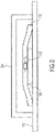
- FIG. 2 shows a schematic cross-sectional view of a device with a printed circuit board 18 on which a microcontroller 16 is arranged.
- the microcontroller 16 is covered by the carrier 12 with circuit structures 13 and is analogous to 1 educated.
- a protective device 34 is arranged above the carrier in order to protect the carrier 12 and thus the measured impedance values from influences and/or changes during normal operation.
- the protective device 34 can have a heat-reflecting or opaque property in order to protect the material of the carrier 12 from premature aging and can be rigid in such a way that accidentally touching the protective device 34 does not lead to a deformation of the circuit structures 13 and thus changed impedance values, e.g. during maintenance of a device.
- the protective device 34 can be in the form of a housing or a cover and can be arranged at a distance from the carrier 12 .
- the protective device 34 it is also conceivable for the protective device 34 to be arranged directly on the carrier 12 in the form of a film.
- the film can be made so stiff that either light touches to none relevant change in the impedance values of the circuit structures 13, or that the carrier 12 is only protected from environmental influences such as light and temperature by which the protective device 34 is protected, but touches lead to a change in the impedance values of the circuit structures 13.
- the carrier can be in the form of a film and attached over an area with a number of components that are worth protecting in such a way that access to one or more of the components to be protected from the outside is prevented without the carrier being deformed.
- the carrier with circuit structures can consist of different materials. Among other things, it can be designed to be flexible so that it can be attached to uneven surfaces or components that vary in height.
- the type of data encryption described has the advantage that the cryptographic key itself is not, or does not have to be, deposited or stored in the system. It is derived from the state of the carrier 12 or from the impedances of the circuit structures 13 and consequently cannot be corrupted or read out.
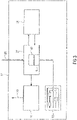
- the carrier 12 covers the microcontroller 16, the JTAG interface 20 it includes, as well as the controller 27 and a flash memory 24 arranged at a distance from the microcontroller 16 and the controller 27.
- the measuring circuit 14 and the analog-to-digital converter 30 are implemented as part of the controller 27 .
- the measurement circuit 14 is part of the module of the control 27 and makes the measurement results available to the analog-to-digital converter 30 implemented as part of the control software.
- the entire device only communicates with other devices via the secure programming interface 28 . All other safety-critical communication interfaces and lines, such as between the flash memory 24 and the controller 27, are covered by the carrier 12 and are inaccessible from the outside.
- the circuit structures 13 can have further signal lines, which are supplied by the controller 27 with signals that vary in amplitude or frequency can be acted upon in order to be able to carry out a challenge-response method and, as explained above, to expand the result space of the measuring circuit 14 .
- the flash memory 24 contains data to be processed by the microcontroller 16 and communicates with it indirectly via the controller 27.
- the controller 27 is able to receive data and programs for the flash memory 24 or the microcontroller 16 via the secure programming interface 28 . However, reading the flash memory 24 or the data or programs located on the microcontroller 16 via the interface 28 is prevented. If data is received from the controller 27 via the secure programming interface 28, the controller 27 encrypts this with a first cryptographic key, which it derives from the impedance values of the circuit structures 13 provided by the measuring circuit 14 and stores them in the encrypted state in the flash memory 24 away.
- the controller 27 If the microcontroller 16 requires data from the flash memory 24, the controller 27 generates a second cryptographic key from the properties of the circuit structures 13, thus decoding the required data from the flash memory 24 and forwards them to the microcontroller 16 Both the data lines from the flash memory 24 to the controller 27 and from the controller 27 to the microcontroller 16 are covered by the carrier 12 and protected from unauthorized access. If the carrier 12 or the circuit structures 13 are manipulated, the measured values provided by the measuring circuit 14 change, and consequently the second cryptographic key, which then differs from the first cryptographic key, which prevents correct decoding of the data from the flash memory 24 . The second cryptographic key is changed at the moment of manipulation, regardless of whether the device is switched on or off. Although the encrypted code can be read out of the flash memory 24 after a manipulation, since the key information of the circuit structures 13 was destroyed by the manipulation that took place, the data are not available in plain text.
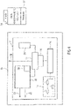
- FIG. 4 shows a schematic representation of a circuit which is mounted on a printed circuit board 18 and a microcontroller 16 with integrated RAM memory, a control unit 27 with an analog-to-digital converter 30, which processes the measured values provided by the measuring circuit 14, a separate flash memory 24, which is accessed by the controller 27, and a secure programming interface 28.
- the microcontroller 16 is shown as a microcontroller without separate protective functions and has a JTAG interface 20 and an ISP interface 22. All components of the circuit, with the exception of the secure programming interface sISP 28, are covered by the carrier 12 with circuit structures 13.
- the flash memory 24 contains all data and/or program sequences in an encrypted state.
- the controller 27 can be implemented, for example, by an FPGA (Field Programmable Gate Array) or an ASIC (Application Specific Integrated Circuit).
- Firmware received via the secure programming interface 28 and/or other data worthy of protection is encrypted by the controller 27 with a first cryptographic key, which it derives from the impedance values of the circuit structures 13 provided by the measuring circuit 14 .
- data and/or code sequences required by the microcontroller 16 are read out from the flash memory 24 by the controller 27 and decrypted using a second cryptographic key.
- the controller 27 makes the decoded data and/or code sequences available to the microcontroller 16 .
- the data lines from the flash memory 24 to the controller 27 and from the controller 27 to the microcontroller 16 are covered by the carrier 12 with the circuit structures 13, so that the data transmitted in plain text from the controller 27 to the microcontroller 16 are protected against access. until the wearer is tampered with.
- the impedance values of the circuit structures 13 change, which prevents decoding and tapping of decrypted data.
- the data is always transferred from the flash memory 24 to the microcontroller 16 via the controller 27.
- the controller 27 appears transparent to the microcontroller 16 because the data is passed on in plain text.
- An advantage of this embodiment is that the RAM memory 26 of the microcontroller only contains the parts of unencrypted code and/or unencrypted data used by the microcontroller 16 at the current runtime. If manipulation is detected, these can be deleted by a dedicated action of the microcontroller, e.g. a power reset or a restart.
- This exemplary embodiment has a higher level of security than the previous embodiment, since data stored in flash memory 24 can be fully encrypted. Alternatively, only parts of the data can be encrypted.
- the actual functionality and intelligence of an embedded system is often in the firmware 32.
- the memory 24 or 26 is protected against a Reading out the firmware 32 aimed for.
- Two systems with different security levels can be implemented here, as 1 and 4 demonstrate.
- the embodiment in 4 has the higher security level of the two exemplary embodiments.
- the system consists of a microcontroller 16 with internal RAM memory 26 and external flash memory 24. This variant is more resource-intensive since all data is encrypted in 1 only part of the firmware 32 is kept decrypted in the RAM memory 26 due to performance and resource optimization, since only code to the extent of the RAM memory 26 can be decrypted in one piece. If the program in the RAM memory 26 has been processed and a further program block is required by the microcontroller 16, the program part in the RAM 26 must be discarded in order to be able to decode the new one.
- temporary memory used by the microcontroller was and is always described as RAM memory in the previous and following exemplary embodiments, such a temporary memory can also be implemented in the form of registers or other temporary memories.
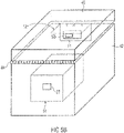
- FIG. 5a shows the schematic representation of a device 40 with an electronic seal system.
- a housing cover 46 is arranged on a housing body 42 via a hinge 44 so that the housing cover can be opened in direction 48 .
- a carrier 12 with circuit structures 13 is arranged on the inside of the housing between the housing body 42 and the housing cover 46 arranged movably relative to it. If the cover 46 is now moved in direction 48, the resulting gap between the housing body 42 and the housing cover 46 leads to a deformation of the carrier 12 and thus to a change in the impedance values of the circuit structures 13.
- Such a device can be used, for example, to determine whether a housing 42/46 was opened between a first point in time, for example a delivery, and a second point in time, for example a delivery or maintenance, and the seal was thus broken. If the impedance values of the circuit structures 13 on the carrier 12 are read out at the first point in time and stored in a type of key, then this value can be compared with the impedance values read out at a second point in time.
- a piece of equipment or circuit 51 arranged inside the housing makes an action dependent on whether the measured impedance values change of the circuit structures 13 change. For example, live parts inside the housing 42/46 can be de-energized. It is also conceivable that opening the housing 42/46 leads to the deletion of sensitive data, or that this event is recorded in a memory of a component inside the housing 42/46.
- Figure 5b shows a schematic interior view of the device 40 with a carrier 12 with circuit structures 13, which includes an RFID tag 52, which contains the measuring circuit 14 and is able to be used with equipment 51 located in the housing body 42 and/or a different type of electronic To communicate system and tell her the measured impedances of the circuit structures 13 of the carrier 12.
- the equipment 51 includes the controller 27 for evaluating the impedance values. If the device 51 has network access, it can inform other network participants or possibly an administrative unit of the detected breach of seal in the event of a seal breach.
- the housing formed by the housing body 42, the hinge 44 and the housing cover 46 is a shipping container, for example, and the electronic equipment 51 notifies the sender and/or the recipient of the container if the container has been opened without authorization.
- Another possible area of application is, for example, new electricity meters or smart meters that allow the electricity network operator to check the status of the sealing seal in the form of the carrier 12 via remote access. A manipulation of the carrier 12 can be detected both locally and remotely.
- a piece of equipment 51 can communicate via any type of communication channel.
- This can be, for example, a network connection, a radio and/or other wireless connection.
- Manipulation or a broken seal can be queried by other communication partners via a communication device, or they can be informed independently of an external query, which can save time.
- the communication between the RFID tag 52 and the equipment 51 and/or another type of electronic system was shown as a wireless communication path, the communication can in principle also be implemented using a wire.
- this invention enables the know-how contained in a firmware 32 to be safeguarded by means of targeted reactions to a breach of the seal, which are not only limited to visual and local detections, but can also actively counteract this.
- breaches of the seals may also be recorded to enable later dating of the event or events.
- FIG. 6 shows a system 70 and the use of the carrier 12 with circuit structures 13 as electronic contact detection.
- a socket 72 is coated with the carrier 12a and the circuit structures 13a, whose impedance values are measured by evaluation electronics 14 inside the system 70. If a plug 64 is then inserted with its plug contacts 62 into the socket housing 72 with the socket contacts 74, the electronic properties of the circuit structures 13a, which are located on the carrier 12a, change due to the mechanical contact, which may lead to slight scratches. An authorized person can then calibrate the overall system 70 to the current state of the circuit structures 13a on the carrier 12a and thus activate the overall system 70. Removing and reinserting the plug 64 causes the measured impedance values to change again due to renewed mechanical stress on the carrier 12a.
- a carrier 12b may be located on the plug 64 and/or the plug contacts 62, allowing a determination of whether the plug was inserted into an unauthorized system between a first and a second point in time.
- the carrier material can be in the form of a foil or membrane or in some other form.
- the arrangement of the carrier 12 can also include an embodiment of the carrier as a solid body, in which the plug 64 or the socket 72 is formed entirely or partially from the carrier material.
- a carrier 12 can also be subsequently integrated into a system at any time after a component has been produced.
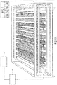
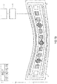
- Figure 7a and 7b each show a representation of a carrier 12 with circuit structures 13, in which the circuit structures 13 are embedded in the material of the carrier 12 and their impedance values are made available to the controller 27 via the measuring circuit 14. If the arrangement of the conductor tracks of the circuit structure 13 relative to one another changes as a result of deformation, as in Figure 7b shown, the impedance values that are detected between the individual conductor tracks by the measuring circuit 14 also change.
- Embedding the circuit structures 13 in the material of the carrier 12 can be advantageous in order to avoid accidental damage to the conductor tracks, for example by touching them during assembly.
- the circuit structures 13 can also be arranged on the carrier 12 .
- microcontroller was only described with JTAG or ISP interfaces in previous exemplary embodiments, the microcontroller can also include other interfaces for programming or reading out memory components, which can be protected by a carrier with circuit structures.
- circuit structures that are on the carrier differentially, in order to possibly obtain greater independence of the results of the impedance measurements from temperature fluctuations. It is also conceivable that the circuit structures, which are located in or on the carrier, are designed in the form of printed electrodes. Due to the surface properties of the carrier material that are difficult to reproduce and the edges of the electrodes that run slightly during the printing process and the associated different impedance values of the circuit structures, this method can lead to a further diversification of the cryptographic keys.
- exemplary embodiments of the protection system described can include the following primary components, which can be used to implement the protection mechanism: A first primary component, a carrier, which can be designed as a protective film, with circuit structures and impedances integrated therein.
- the protective film can have applied or integrated circuit structures with complex impedances.
- the carrier ideally consists of a flexible plastic that can be adapted to the shape of the components to be protected.
- the impedances can be realized through a suitable combination of conductive, semiconductive or insulating components.
- the electrodes can be provided with a protective shield to increase the reproducibility of the measured values.
- a second primary component, the measurement circuit is implemented in such a way that it can detect the impedances of the circuit structures to be measured.
- the impedance results from the resistance, the capacitance and the inductance of the circuit.
- a third primary component, the measurement data processing for example in the form of an analog-to-digital converter, is used on the one hand to digitize the measurement values and on the other hand to stabilize them by suppressing ambient noise and other unwanted interference signals.
- the measurement preparation can be implemented in software using a microcontroller with analog-to-digital converter and an interference suppression algorithm. If there are higher performance and security requirements, the measurement data can be processed can also be implemented in an FPGA or ASIC.
- the primary components of key generation and data encryption can then be integrated in this module together with the measurement data processing.
- a fourth primary component, key generation uses the evaluation of the capacitive properties of the carrier.
- the circuit structures are excited by the signal generator circuit and the recorded and processed measurement data are evaluated using a special algorithm.
- This mechanism acts like a "challenge-response procedure": the excitation by the signal generator circuit is sent as a challenge to the circuit structures, which reacts with a corresponding system response, depending on the input signal and membrane properties.
- the excitation by the signal generator circuit is sent as a challenge to the circuit structures, which reacts with a corresponding system response, depending on the input signal and membrane properties.
- the key generation can also be implemented in software for cost reasons or in hardware - FPGA or ASIC - for performance reasons.
- a fifth primary component, data encryption, is used to completely or partially encrypt the firmware that is loaded into the microcontroller and is part of the control that carries out the data transfer to processors and memory.
- a sixth primary component, data decryption, is the unit in which the encrypted data is decrypted again to run the application and may be implemented as part of the controller.
- a seventh primary component, the communication interface offers the possibility of querying the status of the carrier - intact or damaged - from the outside, provided that the device to be protected is operated in a network. If the carrier is tampered with, the program worthy of protection cannot be correctly decrypted as a result of incorrect key extraction. Only an emergency application is then started, which informs the other participants in the network about the manipulated hardware.
- the firmware can be read, but it is encrypted or partially encrypted in the flash memory and is therefore unusable for the attacker.
- the invention is used as a seal in product tracking or manipulation detection.
- the invention provides the basis for a basic technology for creating a secure, distributed production environment, since not only components but also data lines and storage can be protected against manipulation and unauthorized access. Protection against manipulation enables secure networking, since information processing and storage in the system components is already secured.
Landscapes
- Engineering & Computer Science (AREA)
- Theoretical Computer Science (AREA)
- Computer Hardware Design (AREA)
- Computer Security & Cryptography (AREA)
- Software Systems (AREA)
- General Engineering & Computer Science (AREA)
- Physics & Mathematics (AREA)
- General Physics & Mathematics (AREA)
- Microelectronics & Electronic Packaging (AREA)
- Computer Networks & Wireless Communication (AREA)
- Signal Processing (AREA)
- Mathematical Physics (AREA)
- Storage Device Security (AREA)
- Semiconductor Integrated Circuits (AREA)
Claims (18)
- Dispositif aux caractéristiques suivantes:un support (12) avec des structures de circuit (13) qui présentent une impédance complexe;un moyen de mesure (14) qui est conçu pour mesurer l'impédance complexe des structures de circuit (13) à un premier moment pour obtenir un premier résultat, et pour la mesurer à un deuxième moment ultérieur pour obtenir un deuxième résultat;un moyen de commande (27) qui est configuré pour permettre un fonctionnement d'un composant ou pour évaluer s'il s'est produit un accès non autorisé au composant indépendamment du fait que le premier résultat coïncide ou non avec le deuxième résultat;dans lequel le moyen de commande (27) est conçu pour dériver une clé cryptographique du deuxième résultat; etdans lequel le moyen de commande (27) présente par ailleurs un moyen cryptographique qui est conçu pour décrypter par segment ou complètement un programme crypté mémorisé sur le composant à l'aide de la clé cryptographique;dans lequel l'impédance complexe détectée par le moyen de mesure (14) est une grandeur bidimensionnelle avec une partie imaginaire différente de zéro et une partie réelle différente de zéro, dans lequel le moyen de mesure (14) est conçu pour détecter la partie réelle et la partie imaginaire de l'impédance complexe des structures de circuit (13).
- Dispositif selon la revendication 1, dans lequel la clé cryptographique est une deuxième clé cryptographique, et dans lequel le moyen de commande (27) est conçu pour dériver une première clé cryptographique du premier résultat;
dans lequel le moyen cryptographique est conçu pour utiliser la première clé cryptographique pour crypter un programme ou des données à mémoriser de forme cryptée sur le composant. - Dispositif selon la revendication 1 ou 2, dans lequel le moyen de mesure (14) est conçu pour mesurer l'impédance complexe, dans lequel l'impédance complexe résulte d'une résistance, d'une capacité et d'une inductance des structures de circuit (13).
- Dispositif selon l'une des revendications précédentes, dans lequel le moyen de mesure (14) est conçu pour détecter les valeurs d'impédance complexes entre les pistes conductrices individuelles des structures de circuit (13).
- Dispositif selon l'une des revendications précédentes, dans lequel le moyen de mesure (14) est conçu pour soumettre les structures de circuit (13) à des courbes de tension variant en amplitude et/ou en fréquence et pour recevoir la réponse de système des structures de circuit.
- Dispositif selon l'une des revendications précédentes, dans lequel le support (12) et les structures de circuit (13) présentent une flexibilité telle que le support (12) avec les structures de circuit (13) peut être placé sur une surface irrégulière du composant.
- Dispositif selon l'une des revendications 1 à 6, dans lequel le support (12) est disposé en forme de film de manière à recouvrir les zones du composant à protéger, de sorte que soit empêché un accès aux zones à protéger depuis l'extérieur sans déformation du support.
- Dispositif selon l'une des revendications 1 à 5, dans lequel le support (12) représente un sceau électronique, et dans lequel le moyen de commande (27) est configuré pour évaluer, indépendamment du fait que le premier résultat coïncide ou non avec le deuxième résultat, si le sceau électronique a été rompu ou non.
- Dispositif selon la revendication 8, dans lequel le support (12) est disposé sur deux parties (42; 46) déplaçables l'une par rapport à l'autre du composant.
- Dispositif selon l'une des revendications précédentes, dans lequel le moyen de mesure (14) est conçu pour mesurer de manière répétée l'impédance de la structure de circuit (13) pour obtenir d'autres résultats, et dans lequel le moyen de commande (27) est conçu pour provoquer un redémarrage ou une réinitialisation du courant d'alimentation du composant si un autre résultat ne coïncide pas avec le premier résultat ou un résultat précédent.
- Dispositif selon l'une des revendications précédentes, dans lequel le moyen de commande (27) est conçu pour déplacer le composant dans un mode sécurisé dans lequel ne sont pas requises de séquences de programme ou de données décryptées si un autre résultat ne coïncide pas avec le premier résultat ou un résultat précédent.
- Dispositif selon l'une des revendications 1 à 11, dans lequel un circuit qui présente les structures de circuit (13) est construit de manière différentielle.
- Dispositif selon l'une des revendications 1 à 12, dans lequel les structures de circuit (13) sont réalisées par des électrodes imprimées.
- Dispositif selon l'une des revendications 1 à 13, dans lequel le support (12) est constitué d'un matériau de support dans lequel est introduit un matériau granulaire conducteur et/ou non conducteur.
- Dispositif selon l'une des revendications 1 à 14, dans lequel le dispositif présente une interface de communication qui est conçue pour communiquer aux partenaires de communication d'un système global une discordance entre une mesure et une mesure précédente en ce qui concerne les valeurs d'impédance du support (12) avec les structures de circuit (13).
- Dispositif selon l'une des revendications précédentes, dans lequel est prévu sur le support (12) un moyen de protection (34) qui est conçu pour protéger le support (12) et, de ce fait, les valeurs d'impédance mesurées contre les influences et/ou les modifications pendant le fonctionnement normal.
- Dispositif selon l'une des revendications précédentes, dans lequel le support (12) est formé sur une fiche (64) et/ou une prise de courant (72) et dans lequel une opération de branchement de la fiche (64) avec la prise de courant (72) peut être détectée sur base des modifications provoquées par l'opération de branchement et/ou l'opération de débranchement sur le matériau de support et/ou sur la structure de circuit (13) par le moyen de commande (27) sur base des valeurs de mesure modifiées du moyen de mesure (14).
- Procédé aux étapes suivantes consistant à:mesurer une impédance complexe des structures de circuit (13) sur un support (12) à un deuxième moment pour obtenir un deuxième résultat; où l'impédance complexe est une grandeur bidimensionnelle présentant une partie imaginaire différente de zéro et une partie réelle différente de zéro, et où sont détectées la partie réelle et la partie imaginaire de l'impédance complexe des structures de circuit;permettre un fonctionnement d'un composant ou évaluer s'il s'est produit un accès non autorisé au composant indépendamment du fait que le deuxième résultat coïncide ou non avec le premier résultat à un premier résultat mesuré à un premier moment;dériver une clé cryptographique du deuxième résultat; etdécrypter un programme crypté mémorisé sur le composant par segment ou complètement à l'aide de la clé cryptographique.
Applications Claiming Priority (2)
| Application Number | Priority Date | Filing Date | Title |
|---|---|---|---|
| DE102013205729.6A DE102013205729A1 (de) | 2013-03-28 | 2013-03-28 | Vorrichtung und Verfahren mit einem Träger mit Schaltungsstrukturen |
| PCT/EP2014/055123 WO2014154504A2 (fr) | 2013-03-28 | 2014-03-14 | Dispositif et procédé avec un support présentant des structures de commutation |
Publications (2)
| Publication Number | Publication Date |
|---|---|
| EP2979100A2 EP2979100A2 (fr) | 2016-02-03 |
| EP2979100B1 true EP2979100B1 (fr) | 2022-11-30 |
Family
ID=50389401
Family Applications (1)
| Application Number | Title | Priority Date | Filing Date |
|---|---|---|---|
| EP14713050.4A Active EP2979100B1 (fr) | 2013-03-28 | 2014-03-14 | Dispositif et procédé avec un support présentant des structures de commutation |
Country Status (4)
| Country | Link |
|---|---|
| US (1) | US10592665B2 (fr) |
| EP (1) | EP2979100B1 (fr) |
| DE (1) | DE102013205729A1 (fr) |
| WO (1) | WO2014154504A2 (fr) |
Families Citing this family (19)
| Publication number | Priority date | Publication date | Assignee | Title |
|---|---|---|---|---|
| US11462437B2 (en) | 2013-01-05 | 2022-10-04 | Frederick A. Flitsch | Customized smart devices and touchscreen devices and cleanspace manufacturing methods to make them |
| US12189828B2 (en) | 2013-01-05 | 2025-01-07 | Frederick A. Flitsch | Customized smart devices and touchscreen devices and cleanspace manufacturing methods to make them |
| CN106029516B (zh) * | 2015-01-30 | 2018-09-07 | 诺基亚通信公司 | 用于篡改检测的方法和装置 |
| DE102016207339A1 (de) * | 2016-04-29 | 2017-11-02 | Volkswagen Aktiengesellschaft | Verfahren zur sicheren Interaktion eines Nutzers mit einem mobilen Endgerät und einer weiteren Instanz |
| US20170364683A1 (en) * | 2016-06-17 | 2017-12-21 | Google Inc. | Computing device secure boot |
| US10395064B2 (en) * | 2016-09-02 | 2019-08-27 | Frederick A. Flitsch | Customized smart devices and touchscreen devices and clean space manufacturing methods to make them |
| US10373159B2 (en) * | 2016-12-07 | 2019-08-06 | International Business Machines Corporation | Concomitance of an asset and identity block of a blockchain |
| CN108270569A (zh) * | 2016-12-30 | 2018-07-10 | 航天信息股份有限公司 | 一种通过安全接口进行电子签章的方法及系统 |
| US10547461B2 (en) * | 2017-03-07 | 2020-01-28 | Nxp B.V. | Method and apparatus for binding stacked die using a physically unclonable function |
| DE102017009315B4 (de) | 2017-10-06 | 2019-11-21 | Sergej Gertje | Schutz automatisierungstechnischer Programme vor Umkehrentwicklung |
| EP3550475A1 (fr) * | 2018-04-06 | 2019-10-09 | Fraunhofer-Gesellschaft zur Förderung der angewandten Forschung e.V. | Film puf et son procédé de production |
| EP3550623B1 (fr) | 2018-04-06 | 2020-07-29 | Fraunhofer-Gesellschaft zur Förderung der angewandten Forschung e.V. | Film puf et son procédé de production |
| EP3550466B1 (fr) | 2018-04-06 | 2023-08-02 | Fraunhofer-Gesellschaft zur Förderung der angewandten Forschung e.V. | Film puf et son procédé de production |
| US11213158B2 (en) | 2018-08-29 | 2022-01-04 | Breville USA, Inc. | Cooking system |
| GB201919297D0 (en) | 2019-12-24 | 2020-02-05 | Aronson Bill | Temperature sensing physical unclonable function (puf) authenication system |
| US11516028B2 (en) | 2019-12-24 | 2022-11-29 | CERA Licensing Limited | Temperature sensing physical unclonable function (PUF) authentication system |
| EP3916609A1 (fr) * | 2020-05-29 | 2021-12-01 | Thales Nederland B.V. | Système de circuit protégé et procédé de fonctionnement |
| EP3916608A1 (fr) * | 2020-05-29 | 2021-12-01 | Thales Nederland B.V. | Système de circuit protégé et procédé de fonctionnement |
| FR3111737B1 (fr) * | 2020-06-19 | 2022-07-08 | Commissariat Energie Atomique | Protection de puce ou de boitier-systeme utilisant l’effet gmi |
Family Cites Families (51)
| Publication number | Priority date | Publication date | Assignee | Title |
|---|---|---|---|---|
| US5831531A (en) * | 1992-07-27 | 1998-11-03 | Micron Communications, Inc. | Anti-theft method for detecting the unauthorized opening of containers and baggage |
| GB2297540B (en) | 1993-03-12 | 1997-01-29 | Gore & Ass | Tamper respondent enclosure |
| FR2738971B1 (fr) | 1995-09-19 | 1997-10-10 | Schlumberger Ind Sa | Procede de determination d'une cle de cryptage associee a un circuit integre |
| IL126008A (en) * | 1998-08-31 | 2003-10-31 | Hi G Tek | Electronic monitoring apparatus |
| WO2000016284A1 (fr) * | 1998-09-11 | 2000-03-23 | Key-Trak, Inc. | Detection et prevention de fraudes pour systeme de commande et de reperage d'objets |
| DE19855209A1 (de) | 1998-11-30 | 2000-06-08 | Digital Design Gmbh | Verfahren und Vorrichtung zum Schutz von Gegenständen oder Informationen gegen unberechtigten Zugriff |
| JP3339443B2 (ja) * | 1999-01-18 | 2002-10-28 | 日本電気株式会社 | 機密保護機能付データ保持装置 |
| US7005733B2 (en) * | 1999-12-30 | 2006-02-28 | Koemmerling Oliver | Anti tamper encapsulation for an integrated circuit |
| GB2363233B (en) | 2000-05-11 | 2004-03-31 | Ibm | Tamper resistant card enclosure with improved intrusion detection circuit |
| GB0012478D0 (en) | 2000-05-24 | 2000-07-12 | Ibm | Intrusion detection mechanism for cryptographic cards |
| US6686539B2 (en) | 2001-01-03 | 2004-02-03 | International Business Machines Corporation | Tamper-responding encapsulated enclosure having flexible protective mesh structure |
| US6836843B2 (en) * | 2001-06-29 | 2004-12-28 | Hewlett-Packard Development Company, L.P. | Access control through secure channel using personal identification system |
| US7065656B2 (en) * | 2001-07-03 | 2006-06-20 | Hewlett-Packard Development Company, L.P. | Tamper-evident/tamper-resistant electronic components |
| US20030011474A1 (en) * | 2001-07-13 | 2003-01-16 | Ng Sing King | Circuit and method for electronic security seal |
| FR2831667B1 (fr) * | 2001-10-29 | 2004-04-23 | Cegelec | Capteur pour la detection de defauts dans une piece |
| US20040048877A1 (en) * | 2002-05-22 | 2004-03-11 | Boehringer Ingelheim Pharma Gmbh & Co. Kg | Pharmaceutical compositions containing flibanserin |
| US7098792B1 (en) * | 2003-05-14 | 2006-08-29 | Rf Technologies, Inc. | Tamper proof system and method |
| WO2004114240A2 (fr) * | 2003-06-13 | 2004-12-29 | Xtec, Incorporated | Lecteur differentiel d'identification de frequences hertziennes |
| EP1644873B1 (fr) * | 2003-07-10 | 2012-03-14 | UPM RFID Oy | Modification d'un transpondeur d'identification radiofrequence en cours d'usage |
| JP4748929B2 (ja) * | 2003-08-28 | 2011-08-17 | パナソニック株式会社 | 保護回路および半導体装置 |
| US8169318B2 (en) * | 2003-08-29 | 2012-05-01 | Mikoh Corporation | Radio frequency identification tag with tamper detection capability |
| FR2864667B1 (fr) * | 2003-12-29 | 2006-02-24 | Commissariat Energie Atomique | Protection d'une puce de circuit integre contenant des donnees confidentielles |
| WO2005079223A2 (fr) * | 2004-02-13 | 2005-09-01 | Avery Dennison Corporation | Article de surveillance des sabotages, système et procédé |
| US8074082B2 (en) * | 2004-10-08 | 2011-12-06 | Aprolase Development Co., Llc | Anti-tamper module |
| JP2008517508A (ja) * | 2004-10-18 | 2008-05-22 | コーニンクレッカ フィリップス エレクトロニクス エヌ ヴィ | セキュアセンサチップ |
| US7712674B1 (en) * | 2005-02-22 | 2010-05-11 | Eigent Technologies Llc | RFID devices for verification of correctness, reliability, functionality and security |
| US7281667B2 (en) * | 2005-04-14 | 2007-10-16 | International Business Machines Corporation | Method and structure for implementing secure multichip modules for encryption applications |
| US7215201B2 (en) * | 2005-06-20 | 2007-05-08 | Texas Instruments Norway As | Integrated circuit having a low power, gain-enhanced, low noise amplifying circuit |
| WO2007019642A1 (fr) * | 2005-08-18 | 2007-02-22 | Bioloop Pty Ltd | Agencement et système pour la détection de la falsification |
| US20070271596A1 (en) * | 2006-03-03 | 2007-11-22 | David Boubion | Security, storage and communication system |
| WO2007116355A2 (fr) * | 2006-04-11 | 2007-10-18 | Koninklijke Philips Electronics N.V. | Detection d'attaque avec des puf de nappage |
| WO2007116368A1 (fr) * | 2006-04-11 | 2007-10-18 | Koninklijke Philips Electronics N.V. | Authentification d'une fonction puf basse puissance bruitée sans base de données |
| US7881882B2 (en) * | 2006-09-25 | 2011-02-01 | Ut-Battelle, Llc | Apparatus and method for detecting tampering in flexible structures |
| US8138768B2 (en) * | 2007-01-30 | 2012-03-20 | Nxp B.V. | Sensing circuit for devices with protective coating |
| CN101315401A (zh) * | 2007-05-31 | 2008-12-03 | 安捷伦科技有限公司 | 用于测试一个或多个差分信令通道的开路的方法和装置 |
| US9866370B2 (en) * | 2007-12-05 | 2018-01-09 | Itt Manufacturing Enterprises, Llc | Configurable ASIC-embedded cryptographic processing engine |
| US8026600B2 (en) * | 2008-01-02 | 2011-09-27 | Samsung Electronics Co., Ltd. | Controlled impedance structures for high density interconnections |
| US8427316B2 (en) * | 2008-03-20 | 2013-04-23 | 3M Innovative Properties Company | Detecting tampered with radio frequency identification tags |
| US8077869B2 (en) * | 2008-04-09 | 2011-12-13 | Lockheed Martin Corporation | Organic keyed encryption |
| US7761714B2 (en) * | 2008-10-02 | 2010-07-20 | Infineon Technologies Ag | Integrated circuit and method for preventing an unauthorized access to a digital value |
| US8350704B2 (en) * | 2008-10-03 | 2013-01-08 | Neology, Inc. | Non-transferable radio frequency identification label or tag |
| TWI498827B (zh) * | 2008-11-21 | 2015-09-01 | Verayo Inc | 非連網射頻辨識裝置物理不可複製功能之鑑認技術 |
| CN102265395B (zh) * | 2008-12-29 | 2013-10-16 | Nxp股份有限公司 | 用于物理不可复制功能的物理结构 |
| US8325042B1 (en) * | 2009-02-13 | 2012-12-04 | Impinj, Inc. | RFID tags with differential demodulators |
| US9082057B2 (en) * | 2009-08-19 | 2015-07-14 | Intelleflex Corporation | RF device with tamper detection |
| WO2011128778A2 (fr) * | 2010-04-17 | 2011-10-20 | Paypod, Ltd | Techniques de sécurité pour un terminal de paiement par carte |
| GB2481836B (en) * | 2010-07-08 | 2012-06-13 | Keymat Technology Ltd | Circuit board connector with drilling tamper detection arrangement |
| US8513548B2 (en) * | 2010-07-21 | 2013-08-20 | Maxim Integrated Products, Inc. | Keypad having tamper-resistant keys |
| JP2012053788A (ja) * | 2010-09-02 | 2012-03-15 | Canon Inc | 半導体集積回路装置 |
| DE102010061069A1 (de) * | 2010-12-07 | 2012-06-14 | Wincor Nixdorf International Gmbh | Geldkassette mit elektronischem Siegel |
| WO2014068361A1 (fr) * | 2012-10-29 | 2014-05-08 | Qatar Foundation | Système de détection d'altération |
-
2013
- 2013-03-28 DE DE102013205729.6A patent/DE102013205729A1/de not_active Ceased
-
2014
- 2014-03-14 WO PCT/EP2014/055123 patent/WO2014154504A2/fr not_active Ceased
- 2014-03-14 EP EP14713050.4A patent/EP2979100B1/fr active Active
-
2015
- 2015-09-28 US US14/867,889 patent/US10592665B2/en active Active
Also Published As
| Publication number | Publication date |
|---|---|
| US10592665B2 (en) | 2020-03-17 |
| WO2014154504A3 (fr) | 2015-02-12 |
| US20160092680A1 (en) | 2016-03-31 |
| WO2014154504A2 (fr) | 2014-10-02 |
| EP2979100A2 (fr) | 2016-02-03 |
| DE102013205729A1 (de) | 2014-10-02 |
Similar Documents
| Publication | Publication Date | Title |
|---|---|---|
| EP2979100B1 (fr) | Dispositif et procédé avec un support présentant des structures de commutation | |
| AT408925B (de) | Anordnung zum schutz von elektronischen recheneinheiten, insbesondere von chipkarten | |
| WO2013026663A1 (fr) | Système de transmission sécurisée de données et procédé | |
| DE102013227087A1 (de) | Gesichertes Bereitstellen eines Schlüssels | |
| DE112007002037T5 (de) | Erkennen von auf Strahlung basierenden Angriffen | |
| DE102008051158A1 (de) | Sichere Sensor/Aktor-Systeme | |
| WO2008095866A2 (fr) | Procédé pour autoriser l'accès à au moins un élément d'automatisation d'une installation technique | |
| DE102014208838A1 (de) | Verfahren zum Betreiben eines Steuergeräts | |
| EP2376871B1 (fr) | Procédé de fonctionnement d'un dispositif capteur et dispositif capteur | |
| DE102014208851A1 (de) | Verfahren zum Verhindern eines unbefugten Betriebs eines Kraftfahrzeugs | |
| EP3642812A1 (fr) | Procédé de test de l'intégrité d'un environnement physique dédié à la protection de données | |
| EP1358571B1 (fr) | Dispositif de traitement de donnees | |
| EP2510475B1 (fr) | Dispositif matériel | |
| DE102016118610A1 (de) | Verfahren zur Sicherstellung der Authentizität eines Feldgeräts | |
| EP1664978B1 (fr) | Dispositif et procédé pour éxecuter un programme de manière fiable | |
| DE102015202215A1 (de) | Vorrichtung und Verfahren zum sicheren Betreiben der Vorrichtung | |
| DE102012213155A1 (de) | Vorrichtung mit Sicherheitseinheiten in unterschiedlich geschützten Bereichen | |
| EP3346416B1 (fr) | Module électronique à protection contre les manipulations accrue | |
| EP4373029A1 (fr) | Procédé et dispositif d'authentification d'un composant de fabrication additive | |
| EP3667529B1 (fr) | Procédé et dispositif d'authentification d'une configuration du réseau prédiffusé programmable par l'utilisateur fpga | |
| DE102017009315B4 (de) | Schutz automatisierungstechnischer Programme vor Umkehrentwicklung | |
| DE102012215011A1 (de) | Verfahren und Vorrichtung zum Sichern einer Steuerungseinheit eines Gerätes | |
| DE102014208844A1 (de) | Verfahren zum Durchführen von sicherheitskritischen Vorgängen in einem Steuergerät | |
| WO2013160032A1 (fr) | Procédé de détermination de l'originalité d'un élément structural | |
| EP1674962A1 (fr) | Dispositif de protection des informations enregistrées dans un circuit comprenant des composants électroniques et un processeur. |
Legal Events
| Date | Code | Title | Description |
|---|---|---|---|
| PUAI | Public reference made under article 153(3) epc to a published international application that has entered the european phase |
Free format text: ORIGINAL CODE: 0009012 |
|
| 17P | Request for examination filed |
Effective date: 20151013 |
|
| AK | Designated contracting states |
Kind code of ref document: A2 Designated state(s): AL AT BE BG CH CY CZ DE DK EE ES FI FR GB GR HR HU IE IS IT LI LT LU LV MC MK MT NL NO PL PT RO RS SE SI SK SM TR |
|
| AX | Request for extension of the european patent |
Extension state: BA ME |
|
| DAX | Request for extension of the european patent (deleted) | ||
| STAA | Information on the status of an ep patent application or granted ep patent |
Free format text: STATUS: EXAMINATION IS IN PROGRESS |
|
| 17Q | First examination report despatched |
Effective date: 20181206 |
|
| RAP3 | Party data changed (applicant data changed or rights of an application transferred) |
Owner name: FRAUNHOFER-GESELLSCHAFT ZUR FOERDERUNG DER ANGEWANDTEN FORSCHUNG E.V. |
|
| REG | Reference to a national code |
Ref country code: DE Ref legal event code: R079 Ref document number: 502014016448 Country of ref document: DE Free format text: PREVIOUS MAIN CLASS: G01R0031020000 Ipc: G06F0021860000 |
|
| GRAP | Despatch of communication of intention to grant a patent |
Free format text: ORIGINAL CODE: EPIDOSNIGR1 |
|
| STAA | Information on the status of an ep patent application or granted ep patent |
Free format text: STATUS: GRANT OF PATENT IS INTENDED |
|
| RIC1 | Information provided on ipc code assigned before grant |
Ipc: H01R 13/639 20060101ALI20220510BHEP Ipc: H05K 1/02 20060101ALI20220510BHEP Ipc: H01L 23/00 20060101ALI20220510BHEP Ipc: G01R 31/28 20060101ALI20220510BHEP Ipc: G06F 21/57 20130101ALI20220510BHEP Ipc: G06F 21/55 20130101ALI20220510BHEP Ipc: G06F 21/86 20130101AFI20220510BHEP |
|
| INTG | Intention to grant announced |
Effective date: 20220615 |
|
| GRAS | Grant fee paid |
Free format text: ORIGINAL CODE: EPIDOSNIGR3 |
|
| GRAA | (expected) grant |
Free format text: ORIGINAL CODE: 0009210 |
|
| STAA | Information on the status of an ep patent application or granted ep patent |
Free format text: STATUS: THE PATENT HAS BEEN GRANTED |
|
| AK | Designated contracting states |
Kind code of ref document: B1 Designated state(s): AL AT BE BG CH CY CZ DE DK EE ES FI FR GB GR HR HU IE IS IT LI LT LU LV MC MK MT NL NO PL PT RO RS SE SI SK SM TR |
|
| REG | Reference to a national code |
Ref country code: CH Ref legal event code: EP Ref country code: GB Ref legal event code: FG4D Free format text: NOT ENGLISH |
|
| REG | Reference to a national code |
Ref country code: AT Ref legal event code: REF Ref document number: 1535228 Country of ref document: AT Kind code of ref document: T Effective date: 20221215 Ref country code: DE Ref legal event code: R096 Ref document number: 502014016448 Country of ref document: DE |
|
| REG | Reference to a national code |
Ref country code: IE Ref legal event code: FG4D Free format text: LANGUAGE OF EP DOCUMENT: GERMAN |
|
| REG | Reference to a national code |
Ref country code: NL Ref legal event code: FP |
|
| REG | Reference to a national code |
Ref country code: SE Ref legal event code: TRGR |
|
| REG | Reference to a national code |
Ref country code: LT Ref legal event code: MG9D |
|
| PG25 | Lapsed in a contracting state [announced via postgrant information from national office to epo] |
Ref country code: PT Free format text: LAPSE BECAUSE OF FAILURE TO SUBMIT A TRANSLATION OF THE DESCRIPTION OR TO PAY THE FEE WITHIN THE PRESCRIBED TIME-LIMIT Effective date: 20230331 Ref country code: NO Free format text: LAPSE BECAUSE OF FAILURE TO SUBMIT A TRANSLATION OF THE DESCRIPTION OR TO PAY THE FEE WITHIN THE PRESCRIBED TIME-LIMIT Effective date: 20230228 Ref country code: LT Free format text: LAPSE BECAUSE OF FAILURE TO SUBMIT A TRANSLATION OF THE DESCRIPTION OR TO PAY THE FEE WITHIN THE PRESCRIBED TIME-LIMIT Effective date: 20221130 Ref country code: FI Free format text: LAPSE BECAUSE OF FAILURE TO SUBMIT A TRANSLATION OF THE DESCRIPTION OR TO PAY THE FEE WITHIN THE PRESCRIBED TIME-LIMIT Effective date: 20221130 Ref country code: ES Free format text: LAPSE BECAUSE OF FAILURE TO SUBMIT A TRANSLATION OF THE DESCRIPTION OR TO PAY THE FEE WITHIN THE PRESCRIBED TIME-LIMIT Effective date: 20221130 |
|
| PG25 | Lapsed in a contracting state [announced via postgrant information from national office to epo] |
Ref country code: RS Free format text: LAPSE BECAUSE OF FAILURE TO SUBMIT A TRANSLATION OF THE DESCRIPTION OR TO PAY THE FEE WITHIN THE PRESCRIBED TIME-LIMIT Effective date: 20221130 Ref country code: PL Free format text: LAPSE BECAUSE OF FAILURE TO SUBMIT A TRANSLATION OF THE DESCRIPTION OR TO PAY THE FEE WITHIN THE PRESCRIBED TIME-LIMIT Effective date: 20221130 Ref country code: LV Free format text: LAPSE BECAUSE OF FAILURE TO SUBMIT A TRANSLATION OF THE DESCRIPTION OR TO PAY THE FEE WITHIN THE PRESCRIBED TIME-LIMIT Effective date: 20221130 Ref country code: IS Free format text: LAPSE BECAUSE OF FAILURE TO SUBMIT A TRANSLATION OF THE DESCRIPTION OR TO PAY THE FEE WITHIN THE PRESCRIBED TIME-LIMIT Effective date: 20230330 Ref country code: HR Free format text: LAPSE BECAUSE OF FAILURE TO SUBMIT A TRANSLATION OF THE DESCRIPTION OR TO PAY THE FEE WITHIN THE PRESCRIBED TIME-LIMIT Effective date: 20221130 Ref country code: GR Free format text: LAPSE BECAUSE OF FAILURE TO SUBMIT A TRANSLATION OF THE DESCRIPTION OR TO PAY THE FEE WITHIN THE PRESCRIBED TIME-LIMIT Effective date: 20230301 |
|
| P01 | Opt-out of the competence of the unified patent court (upc) registered |
Effective date: 20230524 |
|
| PG25 | Lapsed in a contracting state [announced via postgrant information from national office to epo] |
Ref country code: SM Free format text: LAPSE BECAUSE OF FAILURE TO SUBMIT A TRANSLATION OF THE DESCRIPTION OR TO PAY THE FEE WITHIN THE PRESCRIBED TIME-LIMIT Effective date: 20221130 Ref country code: RO Free format text: LAPSE BECAUSE OF FAILURE TO SUBMIT A TRANSLATION OF THE DESCRIPTION OR TO PAY THE FEE WITHIN THE PRESCRIBED TIME-LIMIT Effective date: 20221130 Ref country code: EE Free format text: LAPSE BECAUSE OF FAILURE TO SUBMIT A TRANSLATION OF THE DESCRIPTION OR TO PAY THE FEE WITHIN THE PRESCRIBED TIME-LIMIT Effective date: 20221130 Ref country code: DK Free format text: LAPSE BECAUSE OF FAILURE TO SUBMIT A TRANSLATION OF THE DESCRIPTION OR TO PAY THE FEE WITHIN THE PRESCRIBED TIME-LIMIT Effective date: 20221130 Ref country code: CZ Free format text: LAPSE BECAUSE OF FAILURE TO SUBMIT A TRANSLATION OF THE DESCRIPTION OR TO PAY THE FEE WITHIN THE PRESCRIBED TIME-LIMIT Effective date: 20221130 |
|
| PG25 | Lapsed in a contracting state [announced via postgrant information from national office to epo] |
Ref country code: SK Free format text: LAPSE BECAUSE OF FAILURE TO SUBMIT A TRANSLATION OF THE DESCRIPTION OR TO PAY THE FEE WITHIN THE PRESCRIBED TIME-LIMIT Effective date: 20221130 Ref country code: AL Free format text: LAPSE BECAUSE OF FAILURE TO SUBMIT A TRANSLATION OF THE DESCRIPTION OR TO PAY THE FEE WITHIN THE PRESCRIBED TIME-LIMIT Effective date: 20221130 |
|
| REG | Reference to a national code |
Ref country code: DE Ref legal event code: R097 Ref document number: 502014016448 Country of ref document: DE |
|
| PLBE | No opposition filed within time limit |
Free format text: ORIGINAL CODE: 0009261 |
|
| STAA | Information on the status of an ep patent application or granted ep patent |
Free format text: STATUS: NO OPPOSITION FILED WITHIN TIME LIMIT |
|
| PG25 | Lapsed in a contracting state [announced via postgrant information from national office to epo] |
Ref country code: MC Free format text: LAPSE BECAUSE OF FAILURE TO SUBMIT A TRANSLATION OF THE DESCRIPTION OR TO PAY THE FEE WITHIN THE PRESCRIBED TIME-LIMIT Effective date: 20221130 |
|
| REG | Reference to a national code |
Ref country code: CH Ref legal event code: PL |
|
| 26N | No opposition filed |
Effective date: 20230831 |
|
| PG25 | Lapsed in a contracting state [announced via postgrant information from national office to epo] |
Ref country code: SI Free format text: LAPSE BECAUSE OF FAILURE TO SUBMIT A TRANSLATION OF THE DESCRIPTION OR TO PAY THE FEE WITHIN THE PRESCRIBED TIME-LIMIT Effective date: 20221130 |
|
| PG25 | Lapsed in a contracting state [announced via postgrant information from national office to epo] |
Ref country code: LU Free format text: LAPSE BECAUSE OF NON-PAYMENT OF DUE FEES Effective date: 20230314 |
|
| REG | Reference to a national code |
Ref country code: IE Ref legal event code: MM4A |
|
| PG25 | Lapsed in a contracting state [announced via postgrant information from national office to epo] |
Ref country code: LI Free format text: LAPSE BECAUSE OF NON-PAYMENT OF DUE FEES Effective date: 20230331 Ref country code: IE Free format text: LAPSE BECAUSE OF NON-PAYMENT OF DUE FEES Effective date: 20230314 Ref country code: CH Free format text: LAPSE BECAUSE OF NON-PAYMENT OF DUE FEES Effective date: 20230331 |
|
| PG25 | Lapsed in a contracting state [announced via postgrant information from national office to epo] |
Ref country code: BG Free format text: LAPSE BECAUSE OF FAILURE TO SUBMIT A TRANSLATION OF THE DESCRIPTION OR TO PAY THE FEE WITHIN THE PRESCRIBED TIME-LIMIT Effective date: 20221130 |
|
| PG25 | Lapsed in a contracting state [announced via postgrant information from national office to epo] |
Ref country code: BG Free format text: LAPSE BECAUSE OF FAILURE TO SUBMIT A TRANSLATION OF THE DESCRIPTION OR TO PAY THE FEE WITHIN THE PRESCRIBED TIME-LIMIT Effective date: 20221130 |
|
| PGFP | Annual fee paid to national office [announced via postgrant information from national office to epo] |
Ref country code: IT Payment date: 20250331 Year of fee payment: 12 |
|
| PG25 | Lapsed in a contracting state [announced via postgrant information from national office to epo] |
Ref country code: CY Free format text: LAPSE BECAUSE OF FAILURE TO SUBMIT A TRANSLATION OF THE DESCRIPTION OR TO PAY THE FEE WITHIN THE PRESCRIBED TIME-LIMIT; INVALID AB INITIO Effective date: 20140314 |
|
| PG25 | Lapsed in a contracting state [announced via postgrant information from national office to epo] |
Ref country code: HU Free format text: LAPSE BECAUSE OF FAILURE TO SUBMIT A TRANSLATION OF THE DESCRIPTION OR TO PAY THE FEE WITHIN THE PRESCRIBED TIME-LIMIT; INVALID AB INITIO Effective date: 20140314 |
|
| PG25 | Lapsed in a contracting state [announced via postgrant information from national office to epo] |
Ref country code: TR Free format text: LAPSE BECAUSE OF FAILURE TO SUBMIT A TRANSLATION OF THE DESCRIPTION OR TO PAY THE FEE WITHIN THE PRESCRIBED TIME-LIMIT Effective date: 20221130 |
|
| PGFP | Annual fee paid to national office [announced via postgrant information from national office to epo] |
Ref country code: SE Payment date: 20260323 Year of fee payment: 13 |
|
| PGFP | Annual fee paid to national office [announced via postgrant information from national office to epo] |
Ref country code: GB Payment date: 20260324 Year of fee payment: 13 |
|
| PGFP | Annual fee paid to national office [announced via postgrant information from national office to epo] |
Ref country code: DE Payment date: 20260320 Year of fee payment: 13 |
|
| PGFP | Annual fee paid to national office [announced via postgrant information from national office to epo] |
Ref country code: AT Payment date: 20260319 Year of fee payment: 13 |
|
| PGFP | Annual fee paid to national office [announced via postgrant information from national office to epo] |
Ref country code: BE Payment date: 20260323 Year of fee payment: 13 |
|
| PGFP | Annual fee paid to national office [announced via postgrant information from national office to epo] |
Ref country code: NL Payment date: 20260323 Year of fee payment: 13 |
|
| PGFP | Annual fee paid to national office [announced via postgrant information from national office to epo] |
Ref country code: FR Payment date: 20260325 Year of fee payment: 13 |