EP2980282B1 - Monocristaux de semi-conducteur composite pour des éléments de conversion photoélectrique, éléments de conversion photoélectrique et procédé de production de monocristaux de semi-conducteur composite pour des éléments de conversion photoélectrique - Google Patents
Monocristaux de semi-conducteur composite pour des éléments de conversion photoélectrique, éléments de conversion photoélectrique et procédé de production de monocristaux de semi-conducteur composite pour des éléments de conversion photoélectrique Download PDFInfo
- Publication number
- EP2980282B1 EP2980282B1 EP14775557.3A EP14775557A EP2980282B1 EP 2980282 B1 EP2980282 B1 EP 2980282B1 EP 14775557 A EP14775557 A EP 14775557A EP 2980282 B1 EP2980282 B1 EP 2980282B1
- Authority
- EP
- European Patent Office
- Prior art keywords
- photoelectric conversion
- single crystal
- group
- telluride
- melt
- Prior art date
- Legal status (The legal status is an assumption and is not a legal conclusion. Google has not performed a legal analysis and makes no representation as to the accuracy of the status listed.)
- Active
Links
Images
Classifications
-
- H—ELECTRICITY
- H10—SEMICONDUCTOR DEVICES; ELECTRIC SOLID-STATE DEVICES NOT OTHERWISE PROVIDED FOR
- H10F—INORGANIC SEMICONDUCTOR DEVICES SENSITIVE TO INFRARED RADIATION, LIGHT, ELECTROMAGNETIC RADIATION OF SHORTER WAVELENGTH OR CORPUSCULAR RADIATION
- H10F77/00—Constructional details of devices covered by this subclass
- H10F77/10—Semiconductor bodies
- H10F77/16—Material structures, e.g. crystalline structures, film structures or crystal plane orientations
-
- C—CHEMISTRY; METALLURGY
- C30—CRYSTAL GROWTH
- C30B—SINGLE-CRYSTAL GROWTH; UNIDIRECTIONAL SOLIDIFICATION OF EUTECTIC MATERIAL OR UNIDIRECTIONAL DEMIXING OF EUTECTOID MATERIAL; REFINING BY ZONE-MELTING OF MATERIAL; PRODUCTION OF A HOMOGENEOUS POLYCRYSTALLINE MATERIAL WITH DEFINED STRUCTURE; SINGLE CRYSTALS OR HOMOGENEOUS POLYCRYSTALLINE MATERIAL WITH DEFINED STRUCTURE; AFTER-TREATMENT OF SINGLE CRYSTALS OR A HOMOGENEOUS POLYCRYSTALLINE MATERIAL WITH DEFINED STRUCTURE; APPARATUS THEREFOR
- C30B11/00—Single-crystal growth by normal freezing or freezing under temperature gradient, e.g. Bridgman-Stockbarger method
-
- C—CHEMISTRY; METALLURGY
- C30—CRYSTAL GROWTH
- C30B—SINGLE-CRYSTAL GROWTH; UNIDIRECTIONAL SOLIDIFICATION OF EUTECTIC MATERIAL OR UNIDIRECTIONAL DEMIXING OF EUTECTOID MATERIAL; REFINING BY ZONE-MELTING OF MATERIAL; PRODUCTION OF A HOMOGENEOUS POLYCRYSTALLINE MATERIAL WITH DEFINED STRUCTURE; SINGLE CRYSTALS OR HOMOGENEOUS POLYCRYSTALLINE MATERIAL WITH DEFINED STRUCTURE; AFTER-TREATMENT OF SINGLE CRYSTALS OR A HOMOGENEOUS POLYCRYSTALLINE MATERIAL WITH DEFINED STRUCTURE; APPARATUS THEREFOR
- C30B11/00—Single-crystal growth by normal freezing or freezing under temperature gradient, e.g. Bridgman-Stockbarger method
- C30B11/002—Crucibles or containers for supporting the melt
-
- C—CHEMISTRY; METALLURGY
- C30—CRYSTAL GROWTH
- C30B—SINGLE-CRYSTAL GROWTH; UNIDIRECTIONAL SOLIDIFICATION OF EUTECTIC MATERIAL OR UNIDIRECTIONAL DEMIXING OF EUTECTOID MATERIAL; REFINING BY ZONE-MELTING OF MATERIAL; PRODUCTION OF A HOMOGENEOUS POLYCRYSTALLINE MATERIAL WITH DEFINED STRUCTURE; SINGLE CRYSTALS OR HOMOGENEOUS POLYCRYSTALLINE MATERIAL WITH DEFINED STRUCTURE; AFTER-TREATMENT OF SINGLE CRYSTALS OR A HOMOGENEOUS POLYCRYSTALLINE MATERIAL WITH DEFINED STRUCTURE; APPARATUS THEREFOR
- C30B11/00—Single-crystal growth by normal freezing or freezing under temperature gradient, e.g. Bridgman-Stockbarger method
- C30B11/04—Single-crystal growth by normal freezing or freezing under temperature gradient, e.g. Bridgman-Stockbarger method adding crystallising materials or reactants forming it in situ to the melt
- C30B11/06—Single-crystal growth by normal freezing or freezing under temperature gradient, e.g. Bridgman-Stockbarger method adding crystallising materials or reactants forming it in situ to the melt at least one but not all components of the crystal composition being added
- C30B11/065—Single-crystal growth by normal freezing or freezing under temperature gradient, e.g. Bridgman-Stockbarger method adding crystallising materials or reactants forming it in situ to the melt at least one but not all components of the crystal composition being added before crystallising, e.g. synthesis
-
- C—CHEMISTRY; METALLURGY
- C30—CRYSTAL GROWTH
- C30B—SINGLE-CRYSTAL GROWTH; UNIDIRECTIONAL SOLIDIFICATION OF EUTECTIC MATERIAL OR UNIDIRECTIONAL DEMIXING OF EUTECTOID MATERIAL; REFINING BY ZONE-MELTING OF MATERIAL; PRODUCTION OF A HOMOGENEOUS POLYCRYSTALLINE MATERIAL WITH DEFINED STRUCTURE; SINGLE CRYSTALS OR HOMOGENEOUS POLYCRYSTALLINE MATERIAL WITH DEFINED STRUCTURE; AFTER-TREATMENT OF SINGLE CRYSTALS OR A HOMOGENEOUS POLYCRYSTALLINE MATERIAL WITH DEFINED STRUCTURE; APPARATUS THEREFOR
- C30B29/00—Single crystals or homogeneous polycrystalline material with defined structure characterised by the material or by their shape
- C30B29/10—Inorganic compounds or compositions
- C30B29/46—Sulfur-, selenium- or tellurium-containing compounds
- C30B29/48—AIIBVI compounds wherein A is Zn, Cd or Hg, and B is S, Se or Te
-
- H—ELECTRICITY
- H10—SEMICONDUCTOR DEVICES; ELECTRIC SOLID-STATE DEVICES NOT OTHERWISE PROVIDED FOR
- H10F—INORGANIC SEMICONDUCTOR DEVICES SENSITIVE TO INFRARED RADIATION, LIGHT, ELECTROMAGNETIC RADIATION OF SHORTER WAVELENGTH OR CORPUSCULAR RADIATION
- H10F10/00—Individual photovoltaic cells, e.g. solar cells
-
- H—ELECTRICITY
- H10—SEMICONDUCTOR DEVICES; ELECTRIC SOLID-STATE DEVICES NOT OTHERWISE PROVIDED FOR
- H10F—INORGANIC SEMICONDUCTOR DEVICES SENSITIVE TO INFRARED RADIATION, LIGHT, ELECTROMAGNETIC RADIATION OF SHORTER WAVELENGTH OR CORPUSCULAR RADIATION
- H10F10/00—Individual photovoltaic cells, e.g. solar cells
- H10F10/10—Individual photovoltaic cells, e.g. solar cells having potential barriers
- H10F10/16—Photovoltaic cells having only PN heterojunction potential barriers
- H10F10/162—Photovoltaic cells having only PN heterojunction potential barriers comprising only Group II-VI materials, e.g. CdS/CdTe photovoltaic cells
-
- H—ELECTRICITY
- H10—SEMICONDUCTOR DEVICES; ELECTRIC SOLID-STATE DEVICES NOT OTHERWISE PROVIDED FOR
- H10F—INORGANIC SEMICONDUCTOR DEVICES SENSITIVE TO INFRARED RADIATION, LIGHT, ELECTROMAGNETIC RADIATION OF SHORTER WAVELENGTH OR CORPUSCULAR RADIATION
- H10F71/00—Manufacture or treatment of devices covered by this subclass
- H10F71/125—The active layers comprising only Group II-VI materials, e.g. CdS, ZnS or CdTe
- H10F71/1253—The active layers comprising only Group II-VI materials, e.g. CdS, ZnS or CdTe comprising at least three elements, e.g. HgCdTe
-
- H—ELECTRICITY
- H10—SEMICONDUCTOR DEVICES; ELECTRIC SOLID-STATE DEVICES NOT OTHERWISE PROVIDED FOR
- H10F—INORGANIC SEMICONDUCTOR DEVICES SENSITIVE TO INFRARED RADIATION, LIGHT, ELECTROMAGNETIC RADIATION OF SHORTER WAVELENGTH OR CORPUSCULAR RADIATION
- H10F77/00—Constructional details of devices covered by this subclass
- H10F77/10—Semiconductor bodies
- H10F77/12—Active materials
- H10F77/123—Active materials comprising only Group II-VI materials, e.g. CdS, ZnS or HgCdTe
- H10F77/1233—Active materials comprising only Group II-VI materials, e.g. CdS, ZnS or HgCdTe characterised by the dopants
-
- H—ELECTRICITY
- H10—SEMICONDUCTOR DEVICES; ELECTRIC SOLID-STATE DEVICES NOT OTHERWISE PROVIDED FOR
- H10F—INORGANIC SEMICONDUCTOR DEVICES SENSITIVE TO INFRARED RADIATION, LIGHT, ELECTROMAGNETIC RADIATION OF SHORTER WAVELENGTH OR CORPUSCULAR RADIATION
- H10F77/00—Constructional details of devices covered by this subclass
- H10F77/10—Semiconductor bodies
- H10F77/12—Active materials
- H10F77/123—Active materials comprising only Group II-VI materials, e.g. CdS, ZnS or HgCdTe
- H10F77/1237—Active materials comprising only Group II-VI materials, e.g. CdS, ZnS or HgCdTe having at least three elements, e.g. HgCdTe
-
- Y—GENERAL TAGGING OF NEW TECHNOLOGICAL DEVELOPMENTS; GENERAL TAGGING OF CROSS-SECTIONAL TECHNOLOGIES SPANNING OVER SEVERAL SECTIONS OF THE IPC; TECHNICAL SUBJECTS COVERED BY FORMER USPC CROSS-REFERENCE ART COLLECTIONS [XRACs] AND DIGESTS
- Y02—TECHNOLOGIES OR APPLICATIONS FOR MITIGATION OR ADAPTATION AGAINST CLIMATE CHANGE
- Y02E—REDUCTION OF GREENHOUSE GAS [GHG] EMISSIONS, RELATED TO ENERGY GENERATION, TRANSMISSION OR DISTRIBUTION
- Y02E10/00—Energy generation through renewable energy sources
- Y02E10/50—Photovoltaic [PV] energy
- Y02E10/543—Solar cells from Group II-VI materials
-
- Y—GENERAL TAGGING OF NEW TECHNOLOGICAL DEVELOPMENTS; GENERAL TAGGING OF CROSS-SECTIONAL TECHNOLOGIES SPANNING OVER SEVERAL SECTIONS OF THE IPC; TECHNICAL SUBJECTS COVERED BY FORMER USPC CROSS-REFERENCE ART COLLECTIONS [XRACs] AND DIGESTS
- Y02—TECHNOLOGIES OR APPLICATIONS FOR MITIGATION OR ADAPTATION AGAINST CLIMATE CHANGE
- Y02P—CLIMATE CHANGE MITIGATION TECHNOLOGIES IN THE PRODUCTION OR PROCESSING OF GOODS
- Y02P70/00—Climate change mitigation technologies in the production process for final industrial or consumer products
- Y02P70/50—Manufacturing or production processes characterised by the final manufactured product
Definitions
- the at least one group 1A element may be lithium and the concentration of the lithium may range from 2 ⁇ 10 15 cm -3 to 1 ⁇ 10 20 cm -3 .
- any amount of group 1A element can readily be diffused into a single crystal using a stable group 1A element reacting with part of a raw material.
- the hole concentration in a compound semiconductor single crystal ingot of cadmium telluride or cadmium zinc telluride for a photoelectric conversion device can be increased to the range of 4 ⁇ 10 15 cm -3 to 1 ⁇ 10 18 cm -3 which cannot be achieved by any conventional method involving diffusion of impurities from the quartz component.
- the process proceeds to the dicing step.
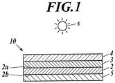
- the ends of the wafer 1 provided with the n-type layer 3, the front electrode 4, and the rear electrode 5 are formed on the main surfaces 1a or 1b is trimmed into one photoelectric conversion device 10, or the wafer 1 is divided into a plurality of substrates 1, 1.. to cut out a plurality of photoelectric conversion devices 10.
- a quartz crucible was filled with 3900 g of polycrystalline CdTe raw material and 1 mg of Na 2 Te, and was placed in an ampule. The ampule was then placed in a VGF furnace to melt the raw material and form a temperature gradient to the melt, so as to grow a single crystal downward from the upper end of the melt.
- the observed surface of the produced CdTe single crystal showed no precipitate.
- the Na and Li concentrations measured in the CdTe single crystal were 1E+16 cm -3 and 2E+15 cm -3 respectively.
- the results demonstrate that the CdTe single crystal produced according to the present embodiment does not contain excess concentrations of impurities.
- the conversion efficiency of the photoelectric conversion device 10 made of Cd(Zn)Te single crystal containing Na and Li as an impurity can be improved.
Landscapes
- Chemical & Material Sciences (AREA)
- Crystallography & Structural Chemistry (AREA)
- Engineering & Computer Science (AREA)
- Materials Engineering (AREA)
- Metallurgy (AREA)
- Organic Chemistry (AREA)
- Inorganic Chemistry (AREA)
- Photovoltaic Devices (AREA)
- Crystals, And After-Treatments Of Crystals (AREA)
- Life Sciences & Earth Sciences (AREA)
- Sustainable Development (AREA)
- Sustainable Energy (AREA)
Claims (8)
- Procédé de production d'un dispositif de conversion photoélectrique (10) comprenant un substrat semi-conducteur de type p découpé dans un lingot de monocristaux de composé semi-conducteur de tellurure de cadmium ou tellurure de cadmium-zinc contenant un ou plusieurs éléments d'impureté du groupe 1A, dans lequel la source d'élément du groupe 1A est du tellurure de lithium, du tellurure de sodium ou à la fois du tellurure de lithium et du tellurure de sodium, le procédé consistant à :remplir un récipient résistant à la chaleur d'une matière première et d'un élément du groupe 1A combiné avec une partie de la matière première, la matière première étant du cadmium et du tellure ou du cadmium, du tellure et du zinc,faire fondre la matière première pour obtenir une masse fondue en chauffant le récipient et diffuser l'élément du groupe 1A dissocié dans la masse fondue,faire croître un monocristal de la masse fondue, dans lequel le monocristal a une concentration en trous comprise entre 4 x 1015 cm-3 et 1 x 1018 cm-3, etdécouper un substrat semi-conducteur de type p (2) dans le monocristal,recouvrir le substrat semi-conducteur de type p (2) ; suivi depolir en miroir le substrat semi-conducteur de type p (2) ; suivi deformer une couche de type n (3) sur une première surface principale (2a) du substrat semi-conducteur de type p (2) ; suivi deformer une électrode avant (4) sur la surface de la couche de type n (3) ; suivi deformer une électrode arrière (5) sur une deuxième surface principale (2b) du substrat semi-conducteur de type p (2),former ainsi un dispositif de conversion photoélectrique (10).
- Procédé selon la revendication 1, dans lequel le ou les éléments du groupe 1A sont du sodium.
- Procédé selon la revendication 1, dans lequel le ou les éléments du groupe 1A sont du sodium et du lithium.
- Procédé selon la revendication 1, dans lequel le ou les éléments du groupe 1A sont du lithium.
- Procédé selon la revendication 1, dans lequel le récipient est composé de nitrure de bore.
- Procédé selon la revendication 1, dans lequel le récipient est composé de quartz.
- Procédé selon la revendication 1, dans lequel la masse fondue est solidifiée par un processus de congélation à gradient vertical.
- Procédé selon la revendication 1, dans lequel la couche de type n (3) est un film mince CdS déposé par épitaxie en phase vapeur, l'électrode avant (4) est un film mince ITO et l'électrode arrière (5) est un film mince de graphite.
Applications Claiming Priority (2)
| Application Number | Priority Date | Filing Date | Title |
|---|---|---|---|
| JP2013072838 | 2013-03-29 | ||
| PCT/JP2014/056230 WO2014156597A1 (fr) | 2013-03-29 | 2014-03-11 | Monocristaux de semi-conducteur composite pour des éléments de conversion photoélectrique, éléments de conversion photoélectrique et procédé de production de monocristaux de semi-conducteur composite pour des éléments de conversion photoélectrique |
Publications (3)
| Publication Number | Publication Date |
|---|---|
| EP2980282A1 EP2980282A1 (fr) | 2016-02-03 |
| EP2980282A4 EP2980282A4 (fr) | 2016-10-05 |
| EP2980282B1 true EP2980282B1 (fr) | 2021-02-24 |
Family
ID=51623580
Family Applications (1)
| Application Number | Title | Priority Date | Filing Date |
|---|---|---|---|
| EP14775557.3A Active EP2980282B1 (fr) | 2013-03-29 | 2014-03-11 | Monocristaux de semi-conducteur composite pour des éléments de conversion photoélectrique, éléments de conversion photoélectrique et procédé de production de monocristaux de semi-conducteur composite pour des éléments de conversion photoélectrique |
Country Status (5)
| Country | Link |
|---|---|
| US (1) | US9362431B2 (fr) |
| EP (1) | EP2980282B1 (fr) |
| JP (1) | JP6149103B2 (fr) |
| TW (1) | TWI544655B (fr) |
| WO (1) | WO2014156597A1 (fr) |
Families Citing this family (1)
| Publication number | Priority date | Publication date | Assignee | Title |
|---|---|---|---|---|
| JP7133476B2 (ja) * | 2018-02-09 | 2022-09-08 | Jx金属株式会社 | テルル化亜鉛カドミウム単結晶基板およびその製造方法 |
Citations (2)
| Publication number | Priority date | Publication date | Assignee | Title |
|---|---|---|---|---|
| US20120024360A1 (en) * | 2010-07-28 | 2012-02-02 | General Electric Company | Photovoltaic device |
| US20120042950A1 (en) * | 2010-06-21 | 2012-02-23 | New Jersey Institute Of Technology | p-Doping of CdTe Polycrystalline Thin Film Based on Cd Vacancy Theory |
Family Cites Families (14)
| Publication number | Priority date | Publication date | Assignee | Title |
|---|---|---|---|---|
| US4734381A (en) * | 1985-10-24 | 1988-03-29 | Atlantic Richfield Company | Method of making a thin film cadmium telluride solar cell |
| JP2708866B2 (ja) * | 1989-03-29 | 1998-02-04 | 三洋電機株式会社 | P型ZnTe単結晶の製造方法 |
| JPH05347425A (ja) | 1992-06-15 | 1993-12-27 | Matsushita Electric Ind Co Ltd | CdS/CdTe太陽電池の製造方法 |
| JP3379054B2 (ja) * | 1994-11-10 | 2003-02-17 | 富士通株式会社 | 半導体結晶の製造方法 |
| JPH0974210A (ja) | 1995-09-04 | 1997-03-18 | Japan Energy Corp | 太陽電池の製造方法 |
| JPH11228299A (ja) | 1998-02-12 | 1999-08-24 | Japan Energy Corp | 化合物半導体単結晶およびその製造方法 |
| JP3916361B2 (ja) * | 2000-02-18 | 2007-05-16 | 独立行政法人科学技術振興機構 | 低抵抗p型単結晶ZnS薄膜およびその製造方法 |
| JP4083449B2 (ja) * | 2002-03-19 | 2008-04-30 | 日鉱金属株式会社 | CdTe単結晶の製造方法 |
| JP2004140038A (ja) | 2002-10-15 | 2004-05-13 | Sumitomo Chem Co Ltd | 薄膜結晶ウェーハの製造方法及び半導体デバイス並びにその製造方法 |
| WO2006054580A1 (fr) * | 2004-11-18 | 2006-05-26 | Nippon Mining & Metals Co., Ltd. | SIMPLE CRISTAL SEMI-CONDUCTEUR EN COMPOSÉ CdTe |
| JP4572963B2 (ja) | 2008-07-09 | 2010-11-04 | 住友電気工業株式会社 | Iii族窒化物系半導体発光素子、及びエピタキシャルウエハ |
| US8618411B2 (en) * | 2009-04-08 | 2013-12-31 | David M. Schwartz | Method of making photovoltaic cell |
| WO2012114803A1 (fr) | 2011-02-24 | 2012-08-30 | Jx日鉱日石金属株式会社 | Poudre et film de tellurure de cadmium destinés à des cellules solaires, et cellule solaire |
| JP2013084921A (ja) * | 2011-09-28 | 2013-05-09 | Fujifilm Corp | 光電変換素子および太陽電池 |
-
2014
- 2014-03-11 EP EP14775557.3A patent/EP2980282B1/fr active Active
- 2014-03-11 WO PCT/JP2014/056230 patent/WO2014156597A1/fr not_active Ceased
- 2014-03-11 US US14/780,921 patent/US9362431B2/en active Active
- 2014-03-11 JP JP2015508251A patent/JP6149103B2/ja active Active
- 2014-03-27 TW TW103111457A patent/TWI544655B/zh active
Patent Citations (2)
| Publication number | Priority date | Publication date | Assignee | Title |
|---|---|---|---|---|
| US20120042950A1 (en) * | 2010-06-21 | 2012-02-23 | New Jersey Institute Of Technology | p-Doping of CdTe Polycrystalline Thin Film Based on Cd Vacancy Theory |
| US20120024360A1 (en) * | 2010-07-28 | 2012-02-02 | General Electric Company | Photovoltaic device |
Non-Patent Citations (2)
| Title |
|---|
| P H YSI ET AL: "Shallow Acceptor States in ZnTe and CdTe", 14 October 1966 (1966-10-14), XP055622179, Retrieved from the Internet <URL:https://journals.aps.org/pr/pdf/10.1103/PhysRev.150.541> [retrieved on 20190913] * |
| PAULI H ET AL: "P-TYPE CDTE EPILAYERS GROWN BY HOT-WALL-BEAM EPITAXY", JOURNAL OF APPLIED PHYSICS, AMERICAN INSTITUTE OF PHYSICS, US, vol. 73, no. 8, 15 April 1993 (1993-04-15), pages 4061 - 4063, XP000361024, ISSN: 0021-8979, DOI: 10.1063/1.352854 * |
Also Published As
| Publication number | Publication date |
|---|---|
| TW201448260A (zh) | 2014-12-16 |
| EP2980282A1 (fr) | 2016-02-03 |
| WO2014156597A1 (fr) | 2014-10-02 |
| EP2980282A4 (fr) | 2016-10-05 |
| TWI544655B (zh) | 2016-08-01 |
| US9362431B2 (en) | 2016-06-07 |
| JPWO2014156597A1 (ja) | 2017-02-16 |
| JP6149103B2 (ja) | 2017-06-14 |
| US20160056313A1 (en) | 2016-02-25 |
Similar Documents
| Publication | Publication Date | Title |
|---|---|---|
| JPH0458193B2 (fr) | ||
| SG178668A1 (en) | Silicon wafer and production method thereof | |
| John et al. | Comprehensive review on CdTe crystals: growth, properties, and photovoltaic application | |
| Zappettini | Cadmium telluride and cadmium zinc telluride | |
| JP6749309B2 (ja) | 化合物半導体ウエハ、および光電変換素子 | |
| JP2005159312A (ja) | 太陽電池用多結晶シリコン基板の母材および太陽電池用多結晶シリコン基板 | |
| Nagaoka et al. | Review on group-V doping in CdTe for photovoltaic application | |
| EP2980282B1 (fr) | Monocristaux de semi-conducteur composite pour des éléments de conversion photoélectrique, éléments de conversion photoélectrique et procédé de production de monocristaux de semi-conducteur composite pour des éléments de conversion photoélectrique | |
| US10134590B2 (en) | Methods of growing CdTe-based materials at high rates | |
| Suda et al. | Zn3P2/ITO heterojunction solar cells | |
| Sekine et al. | Growth and characterization of CdTe single crystals prepared by the “Liquinert Processed” vertical Bridgman method for radiation detectors | |
| EP3218533A1 (fr) | Procede de fabrication d'un lingot de silicium monocristallin de type n | |
| US20130118564A1 (en) | Rare earth sulfide thin films | |
| JP4589400B2 (ja) | 光起電力活性半導体材料を有する光起電力セル | |
| WO2006054580A1 (fr) | SIMPLE CRISTAL SEMI-CONDUCTEUR EN COMPOSÉ CdTe | |
| KR102919820B1 (ko) | Mg2Si 단결정체, Mg2Si 단결정 기판, 적외선 수광 소자 및 Mg2Si 단결정체의 제조 방법 | |
| US20130068156A1 (en) | Method for growing ii-vi semiconductor crystals and ii-vi semiconductor layers | |
| Capper | Narrow bandgap II-VI semiconductors: Growth | |
| Montag et al. | Single Crystal Growth of Arsenic Doped and Phosphorus Doped Cadmium Selenium Telluride (CdSe x Te 1-x) to Improve CdTe Thin Film Photovoltaics | |
| JPH11228299A (ja) | 化合物半導体単結晶およびその製造方法 | |
| JP2008518448A (ja) | 光起電力セル | |
| Sapaev et al. | The synthesis and photoelectric properties of Si-(Si2) 1− x (ZnS) x epitaxial structures | |
| Zhang | Liquid phase epitaxial growth of silicon thin film for solar cell application | |
| Woods | Group II-VI Semiconductors | |
| Hay et al. | CdZnTe for a wide band gap all thin film solar cell |
Legal Events
| Date | Code | Title | Description |
|---|---|---|---|
| PUAI | Public reference made under article 153(3) epc to a published international application that has entered the european phase |
Free format text: ORIGINAL CODE: 0009012 |
|
| 17P | Request for examination filed |
Effective date: 20150924 |
|
| AK | Designated contracting states |
Kind code of ref document: A1 Designated state(s): AL AT BE BG CH CY CZ DE DK EE ES FI FR GB GR HR HU IE IS IT LI LT LU LV MC MK MT NL NO PL PT RO RS SE SI SK SM TR |
|
| AX | Request for extension of the european patent |
Extension state: BA ME |
|
| DAX | Request for extension of the european patent (deleted) | ||
| A4 | Supplementary search report drawn up and despatched |
Effective date: 20160902 |
|
| RIC1 | Information provided on ipc code assigned before grant |
Ipc: C30B 11/00 20060101ALI20160829BHEP Ipc: C30B 29/48 20060101AFI20160829BHEP Ipc: H01L 31/073 20120101ALI20160829BHEP |
|
| STAA | Information on the status of an ep patent application or granted ep patent |
Free format text: STATUS: EXAMINATION IS IN PROGRESS |
|
| 17Q | First examination report despatched |
Effective date: 20181009 |
|
| GRAP | Despatch of communication of intention to grant a patent |
Free format text: ORIGINAL CODE: EPIDOSNIGR1 |
|
| STAA | Information on the status of an ep patent application or granted ep patent |
Free format text: STATUS: GRANT OF PATENT IS INTENDED |
|
| INTG | Intention to grant announced |
Effective date: 20200406 |
|
| GRAJ | Information related to disapproval of communication of intention to grant by the applicant or resumption of examination proceedings by the epo deleted |
Free format text: ORIGINAL CODE: EPIDOSDIGR1 |
|
| STAA | Information on the status of an ep patent application or granted ep patent |
Free format text: STATUS: EXAMINATION IS IN PROGRESS |
|
| GRAS | Grant fee paid |
Free format text: ORIGINAL CODE: EPIDOSNIGR3 |
|
| STAA | Information on the status of an ep patent application or granted ep patent |
Free format text: STATUS: GRANT OF PATENT IS INTENDED |
|
| GRAP | Despatch of communication of intention to grant a patent |
Free format text: ORIGINAL CODE: EPIDOSNIGR1 |
|
| INTC | Intention to grant announced (deleted) | ||
| INTG | Intention to grant announced |
Effective date: 20200916 |
|
| GRAA | (expected) grant |
Free format text: ORIGINAL CODE: 0009210 |
|
| STAA | Information on the status of an ep patent application or granted ep patent |
Free format text: STATUS: THE PATENT HAS BEEN GRANTED |
|
| AK | Designated contracting states |
Kind code of ref document: B1 Designated state(s): AL AT BE BG CH CY CZ DE DK EE ES FI FR GB GR HR HU IE IS IT LI LT LU LV MC MK MT NL NO PL PT RO RS SE SI SK SM TR |
|
| REG | Reference to a national code |
Ref country code: GB Ref legal event code: FG4D |
|
| REG | Reference to a national code |
Ref country code: CH Ref legal event code: EP |
|
| REG | Reference to a national code |
Ref country code: AT Ref legal event code: REF Ref document number: 1364546 Country of ref document: AT Kind code of ref document: T Effective date: 20210315 |
|
| REG | Reference to a national code |
Ref country code: IE Ref legal event code: FG4D |
|
| REG | Reference to a national code |
Ref country code: DE Ref legal event code: R096 Ref document number: 602014075140 Country of ref document: DE |
|
| REG | Reference to a national code |
Ref country code: LT Ref legal event code: MG9D |
|
| REG | Reference to a national code |
Ref country code: NL Ref legal event code: MP Effective date: 20210224 |
|
| PG25 | Lapsed in a contracting state [announced via postgrant information from national office to epo] |
Ref country code: HR Free format text: LAPSE BECAUSE OF FAILURE TO SUBMIT A TRANSLATION OF THE DESCRIPTION OR TO PAY THE FEE WITHIN THE PRESCRIBED TIME-LIMIT Effective date: 20210224 Ref country code: GR Free format text: LAPSE BECAUSE OF FAILURE TO SUBMIT A TRANSLATION OF THE DESCRIPTION OR TO PAY THE FEE WITHIN THE PRESCRIBED TIME-LIMIT Effective date: 20210525 Ref country code: FI Free format text: LAPSE BECAUSE OF FAILURE TO SUBMIT A TRANSLATION OF THE DESCRIPTION OR TO PAY THE FEE WITHIN THE PRESCRIBED TIME-LIMIT Effective date: 20210224 Ref country code: PT Free format text: LAPSE BECAUSE OF FAILURE TO SUBMIT A TRANSLATION OF THE DESCRIPTION OR TO PAY THE FEE WITHIN THE PRESCRIBED TIME-LIMIT Effective date: 20210624 Ref country code: LT Free format text: LAPSE BECAUSE OF FAILURE TO SUBMIT A TRANSLATION OF THE DESCRIPTION OR TO PAY THE FEE WITHIN THE PRESCRIBED TIME-LIMIT Effective date: 20210224 Ref country code: BG Free format text: LAPSE BECAUSE OF FAILURE TO SUBMIT A TRANSLATION OF THE DESCRIPTION OR TO PAY THE FEE WITHIN THE PRESCRIBED TIME-LIMIT Effective date: 20210524 Ref country code: NO Free format text: LAPSE BECAUSE OF FAILURE TO SUBMIT A TRANSLATION OF THE DESCRIPTION OR TO PAY THE FEE WITHIN THE PRESCRIBED TIME-LIMIT Effective date: 20210524 |
|
| REG | Reference to a national code |
Ref country code: AT Ref legal event code: MK05 Ref document number: 1364546 Country of ref document: AT Kind code of ref document: T Effective date: 20210224 |
|
| PG25 | Lapsed in a contracting state [announced via postgrant information from national office to epo] |
Ref country code: SE Free format text: LAPSE BECAUSE OF FAILURE TO SUBMIT A TRANSLATION OF THE DESCRIPTION OR TO PAY THE FEE WITHIN THE PRESCRIBED TIME-LIMIT Effective date: 20210224 Ref country code: PL Free format text: LAPSE BECAUSE OF FAILURE TO SUBMIT A TRANSLATION OF THE DESCRIPTION OR TO PAY THE FEE WITHIN THE PRESCRIBED TIME-LIMIT Effective date: 20210224 Ref country code: LV Free format text: LAPSE BECAUSE OF FAILURE TO SUBMIT A TRANSLATION OF THE DESCRIPTION OR TO PAY THE FEE WITHIN THE PRESCRIBED TIME-LIMIT Effective date: 20210224 Ref country code: NL Free format text: LAPSE BECAUSE OF FAILURE TO SUBMIT A TRANSLATION OF THE DESCRIPTION OR TO PAY THE FEE WITHIN THE PRESCRIBED TIME-LIMIT Effective date: 20210224 Ref country code: RS Free format text: LAPSE BECAUSE OF FAILURE TO SUBMIT A TRANSLATION OF THE DESCRIPTION OR TO PAY THE FEE WITHIN THE PRESCRIBED TIME-LIMIT Effective date: 20210224 |
|
| PG25 | Lapsed in a contracting state [announced via postgrant information from national office to epo] |
Ref country code: IS Free format text: LAPSE BECAUSE OF FAILURE TO SUBMIT A TRANSLATION OF THE DESCRIPTION OR TO PAY THE FEE WITHIN THE PRESCRIBED TIME-LIMIT Effective date: 20210624 |
|
| PG25 | Lapsed in a contracting state [announced via postgrant information from national office to epo] |
Ref country code: AT Free format text: LAPSE BECAUSE OF FAILURE TO SUBMIT A TRANSLATION OF THE DESCRIPTION OR TO PAY THE FEE WITHIN THE PRESCRIBED TIME-LIMIT Effective date: 20210224 Ref country code: EE Free format text: LAPSE BECAUSE OF FAILURE TO SUBMIT A TRANSLATION OF THE DESCRIPTION OR TO PAY THE FEE WITHIN THE PRESCRIBED TIME-LIMIT Effective date: 20210224 Ref country code: CZ Free format text: LAPSE BECAUSE OF FAILURE TO SUBMIT A TRANSLATION OF THE DESCRIPTION OR TO PAY THE FEE WITHIN THE PRESCRIBED TIME-LIMIT Effective date: 20210224 Ref country code: SM Free format text: LAPSE BECAUSE OF FAILURE TO SUBMIT A TRANSLATION OF THE DESCRIPTION OR TO PAY THE FEE WITHIN THE PRESCRIBED TIME-LIMIT Effective date: 20210224 |
|
| REG | Reference to a national code |
Ref country code: CH Ref legal event code: PL |
|
| REG | Reference to a national code |
Ref country code: DE Ref legal event code: R097 Ref document number: 602014075140 Country of ref document: DE |
|
| PG25 | Lapsed in a contracting state [announced via postgrant information from national office to epo] |
Ref country code: SK Free format text: LAPSE BECAUSE OF FAILURE TO SUBMIT A TRANSLATION OF THE DESCRIPTION OR TO PAY THE FEE WITHIN THE PRESCRIBED TIME-LIMIT Effective date: 20210224 Ref country code: RO Free format text: LAPSE BECAUSE OF FAILURE TO SUBMIT A TRANSLATION OF THE DESCRIPTION OR TO PAY THE FEE WITHIN THE PRESCRIBED TIME-LIMIT Effective date: 20210224 Ref country code: MC Free format text: LAPSE BECAUSE OF FAILURE TO SUBMIT A TRANSLATION OF THE DESCRIPTION OR TO PAY THE FEE WITHIN THE PRESCRIBED TIME-LIMIT Effective date: 20210224 Ref country code: DK Free format text: LAPSE BECAUSE OF FAILURE TO SUBMIT A TRANSLATION OF THE DESCRIPTION OR TO PAY THE FEE WITHIN THE PRESCRIBED TIME-LIMIT Effective date: 20210224 Ref country code: ES Free format text: LAPSE BECAUSE OF FAILURE TO SUBMIT A TRANSLATION OF THE DESCRIPTION OR TO PAY THE FEE WITHIN THE PRESCRIBED TIME-LIMIT Effective date: 20210224 |
|
| REG | Reference to a national code |
Ref country code: BE Ref legal event code: MM Effective date: 20210331 |
|
| PLBE | No opposition filed within time limit |
Free format text: ORIGINAL CODE: 0009261 |
|
| STAA | Information on the status of an ep patent application or granted ep patent |
Free format text: STATUS: NO OPPOSITION FILED WITHIN TIME LIMIT |
|
| PG25 | Lapsed in a contracting state [announced via postgrant information from national office to epo] |
Ref country code: CH Free format text: LAPSE BECAUSE OF NON-PAYMENT OF DUE FEES Effective date: 20210331 Ref country code: AL Free format text: LAPSE BECAUSE OF FAILURE TO SUBMIT A TRANSLATION OF THE DESCRIPTION OR TO PAY THE FEE WITHIN THE PRESCRIBED TIME-LIMIT Effective date: 20210224 Ref country code: LI Free format text: LAPSE BECAUSE OF NON-PAYMENT OF DUE FEES Effective date: 20210331 Ref country code: LU Free format text: LAPSE BECAUSE OF NON-PAYMENT OF DUE FEES Effective date: 20210311 Ref country code: IE Free format text: LAPSE BECAUSE OF NON-PAYMENT OF DUE FEES Effective date: 20210311 |
|
| 26N | No opposition filed |
Effective date: 20211125 |
|
| PG25 | Lapsed in a contracting state [announced via postgrant information from national office to epo] |
Ref country code: SI Free format text: LAPSE BECAUSE OF FAILURE TO SUBMIT A TRANSLATION OF THE DESCRIPTION OR TO PAY THE FEE WITHIN THE PRESCRIBED TIME-LIMIT Effective date: 20210224 |
|
| PG25 | Lapsed in a contracting state [announced via postgrant information from national office to epo] |
Ref country code: IT Free format text: LAPSE BECAUSE OF FAILURE TO SUBMIT A TRANSLATION OF THE DESCRIPTION OR TO PAY THE FEE WITHIN THE PRESCRIBED TIME-LIMIT Effective date: 20210224 |
|
| PG25 | Lapsed in a contracting state [announced via postgrant information from national office to epo] |
Ref country code: IS Free format text: LAPSE BECAUSE OF FAILURE TO SUBMIT A TRANSLATION OF THE DESCRIPTION OR TO PAY THE FEE WITHIN THE PRESCRIBED TIME-LIMIT Effective date: 20210624 |
|
| PG25 | Lapsed in a contracting state [announced via postgrant information from national office to epo] |
Ref country code: BE Free format text: LAPSE BECAUSE OF NON-PAYMENT OF DUE FEES Effective date: 20210331 |
|
| PG25 | Lapsed in a contracting state [announced via postgrant information from national office to epo] |
Ref country code: HU Free format text: LAPSE BECAUSE OF FAILURE TO SUBMIT A TRANSLATION OF THE DESCRIPTION OR TO PAY THE FEE WITHIN THE PRESCRIBED TIME-LIMIT; INVALID AB INITIO Effective date: 20140311 |
|
| PG25 | Lapsed in a contracting state [announced via postgrant information from national office to epo] |
Ref country code: CY Free format text: LAPSE BECAUSE OF FAILURE TO SUBMIT A TRANSLATION OF THE DESCRIPTION OR TO PAY THE FEE WITHIN THE PRESCRIBED TIME-LIMIT Effective date: 20210224 |
|
| PG25 | Lapsed in a contracting state [announced via postgrant information from national office to epo] |
Ref country code: MK Free format text: LAPSE BECAUSE OF FAILURE TO SUBMIT A TRANSLATION OF THE DESCRIPTION OR TO PAY THE FEE WITHIN THE PRESCRIBED TIME-LIMIT Effective date: 20210224 |
|
| PG25 | Lapsed in a contracting state [announced via postgrant information from national office to epo] |
Ref country code: TR Free format text: LAPSE BECAUSE OF FAILURE TO SUBMIT A TRANSLATION OF THE DESCRIPTION OR TO PAY THE FEE WITHIN THE PRESCRIBED TIME-LIMIT Effective date: 20210224 |
|
| PG25 | Lapsed in a contracting state [announced via postgrant information from national office to epo] |
Ref country code: MT Free format text: LAPSE BECAUSE OF FAILURE TO SUBMIT A TRANSLATION OF THE DESCRIPTION OR TO PAY THE FEE WITHIN THE PRESCRIBED TIME-LIMIT Effective date: 20210224 |
|
| PGFP | Annual fee paid to national office [announced via postgrant information from national office to epo] |
Ref country code: GB Payment date: 20260202 Year of fee payment: 13 |
|
| PGFP | Annual fee paid to national office [announced via postgrant information from national office to epo] |
Ref country code: DE Payment date: 20260128 Year of fee payment: 13 |
|
| PGFP | Annual fee paid to national office [announced via postgrant information from national office to epo] |
Ref country code: FR Payment date: 20260209 Year of fee payment: 13 |