EP2980975A1 - Systeme und verfahren zur erweiterten diagnose in modularen leistungswandlern - Google Patents
Systeme und verfahren zur erweiterten diagnose in modularen leistungswandlern Download PDFInfo
- Publication number
- EP2980975A1 EP2980975A1 EP15177664.8A EP15177664A EP2980975A1 EP 2980975 A1 EP2980975 A1 EP 2980975A1 EP 15177664 A EP15177664 A EP 15177664A EP 2980975 A1 EP2980975 A1 EP 2980975A1
- Authority
- EP
- European Patent Office
- Prior art keywords
- power conversion
- current
- conversion modules
- accordance
- modules
- Prior art date
- Legal status (The legal status is an assumption and is not a legal conclusion. Google has not performed a legal analysis and makes no representation as to the accuracy of the status listed.)
- Granted
Links
Images




Classifications
-
- G—PHYSICS
- G05—CONTROLLING; REGULATING
- G05F—SYSTEMS FOR REGULATING ELECTRIC OR MAGNETIC VARIABLES
- G05F1/00—Automatic systems in which deviations of an electric quantity from one or more predetermined values are detected at the output of the system and fed back to a device within the system to restore the detected quantity to its predetermined value or values, i.e. retroactive systems
- G05F1/10—Regulating voltage or current
-
- H—ELECTRICITY
- H02—GENERATION; CONVERSION OR DISTRIBUTION OF ELECTRIC POWER
- H02J—ELECTRIC POWER NETWORKS; CIRCUIT ARRANGEMENTS OR SYSTEMS FOR SUPPLYING OR DISTRIBUTING ELECTRIC POWER; SYSTEMS FOR STORING ELECTRIC ENERGY
- H02J4/00—Circuit arrangements for mains or distribution networks not specified as AC or DC; Circuit arrangements for mains or distribution networks combining AC and DC sections or sub-networks
-
- H—ELECTRICITY
- H02—GENERATION; CONVERSION OR DISTRIBUTION OF ELECTRIC POWER
- H02M—APPARATUS FOR CONVERSION BETWEEN AC AND AC, BETWEEN AC AND DC, OR BETWEEN DC AND DC, AND FOR USE WITH MAINS OR SIMILAR POWER SUPPLY SYSTEMS; CONVERSION OF DC OR AC INPUT POWER INTO SURGE OUTPUT POWER; CONTROL OR REGULATION THEREOF
- H02M3/00—Conversion of DC power input into DC power output
- H02M3/02—Conversion of DC power input into DC power output without intermediate conversion into AC
- H02M3/04—Conversion of DC power input into DC power output without intermediate conversion into AC by static converters
- H02M3/10—Conversion of DC power input into DC power output without intermediate conversion into AC by static converters using discharge tubes with control electrode or semiconductor devices with control electrode
- H02M3/145—Conversion of DC power input into DC power output without intermediate conversion into AC by static converters using discharge tubes with control electrode or semiconductor devices with control electrode using devices of a triode or transistor type requiring continuous application of a control signal
- H02M3/155—Conversion of DC power input into DC power output without intermediate conversion into AC by static converters using discharge tubes with control electrode or semiconductor devices with control electrode using devices of a triode or transistor type requiring continuous application of a control signal using semiconductor devices only
- H02M3/156—Conversion of DC power input into DC power output without intermediate conversion into AC by static converters using discharge tubes with control electrode or semiconductor devices with control electrode using devices of a triode or transistor type requiring continuous application of a control signal using semiconductor devices only with automatic control of output voltage or current, e.g. switching regulators
- H02M3/158—Conversion of DC power input into DC power output without intermediate conversion into AC by static converters using discharge tubes with control electrode or semiconductor devices with control electrode using devices of a triode or transistor type requiring continuous application of a control signal using semiconductor devices only with automatic control of output voltage or current, e.g. switching regulators including plural semiconductor devices as final control devices for a single load
- H02M3/1584—Conversion of DC power input into DC power output without intermediate conversion into AC by static converters using discharge tubes with control electrode or semiconductor devices with control electrode using devices of a triode or transistor type requiring continuous application of a control signal using semiconductor devices only with automatic control of output voltage or current, e.g. switching regulators including plural semiconductor devices as final control devices for a single load with a plurality of power processing stages connected in parallel
-
- H—ELECTRICITY
- H02—GENERATION; CONVERSION OR DISTRIBUTION OF ELECTRIC POWER
- H02M—APPARATUS FOR CONVERSION BETWEEN AC AND AC, BETWEEN AC AND DC, OR BETWEEN DC AND DC, AND FOR USE WITH MAINS OR SIMILAR POWER SUPPLY SYSTEMS; CONVERSION OF DC OR AC INPUT POWER INTO SURGE OUTPUT POWER; CONTROL OR REGULATION THEREOF
- H02M7/00—Conversion of AC power input into DC power output; Conversion of DC power input into AC power output
- H02M7/42—Conversion of DC power input into AC power output without possibility of reversal
- H02M7/44—Conversion of DC power input into AC power output without possibility of reversal by static converters
- H02M7/48—Conversion of DC power input into AC power output without possibility of reversal by static converters using discharge tubes with control electrode or semiconductor devices with control electrode
- H02M7/493—Conversion of DC power input into AC power output without possibility of reversal by static converters using discharge tubes with control electrode or semiconductor devices with control electrode the static converters being arranged for operation in parallel
-
- H—ELECTRICITY
- H02—GENERATION; CONVERSION OR DISTRIBUTION OF ELECTRIC POWER
- H02M—APPARATUS FOR CONVERSION BETWEEN AC AND AC, BETWEEN AC AND DC, OR BETWEEN DC AND DC, AND FOR USE WITH MAINS OR SIMILAR POWER SUPPLY SYSTEMS; CONVERSION OF DC OR AC INPUT POWER INTO SURGE OUTPUT POWER; CONTROL OR REGULATION THEREOF
- H02M7/00—Conversion of AC power input into DC power output; Conversion of DC power input into AC power output
- H02M7/42—Conversion of DC power input into AC power output without possibility of reversal
- H02M7/44—Conversion of DC power input into AC power output without possibility of reversal by static converters
- H02M7/48—Conversion of DC power input into AC power output without possibility of reversal by static converters using discharge tubes with control electrode or semiconductor devices with control electrode
- H02M7/483—Converters with outputs that each can have more than two voltages levels
- H02M7/487—Neutral point clamped inverters
Definitions
- the field of the invention relates generally to advanced diagnostics in modular power converters, and more particularly, to current unbalance detection in modular power converters.
- a known power conversion system 10 includes, for each of three phases, three insulated gate bipolar transistor (IGBT) power converters 12 coupled in parallel.
- IGBT insulated gate bipolar transistor
- all paralleled power converters 12 share the same pulse-width modulation (PWM) (i.e., they receive the same PWM control signals), and load sharing is assumed, given characteristics of power converters 12 and geometry of power conversion system 10.
- PWM pulse-width modulation
- a known power conversion system 20 includes, for each of three phases (i.e., U, V, W), a pair of power converters 22 coupled in parallel. In this configuration, all parallel power converters 22 also share the same PWM modulation. Introducing an impedance between paralleled power converters 22 facilitates mitigating potential unbalance due to differences in semiconductor characteristics and/or geometry of system 20.
- current sharing is assumed but is not actively monitored. Accordingly, a load unbalance condition may go undetected, which may lead to premature failure of over-stressed modules.
- FIG. 3 shows a known power conversion system 30 that includes a centralized controller 32 communicatively coupled to a plurality of power conversion modules 34. Centralized controller 32 monitors an output current of each power conversion module 34, as well as a voltage across a load 36, and controls operation of power conversion modules 34 accordingly.
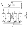
- Fig. 4 shows a known power conversion system 40 that includes a plurality of power conversion modules 42 each including an associated control module 44. Each control module 44 monitors an output current of an associated power conversion module 42, as well as a voltage across a load 46, and controls operation of the associated power conversion modules 42 accordingly.
- such systems may require complex cabling in case of a centralized solution (i.e., system 30), or distributed intelligence in case of decentralized solutions (i.e., system 40).
- a power conversion system in one aspect, includes a plurality of power conversion modules connected in parallel, wherein all power conversion modules of the plurality of power conversion modules are configured to receive a pulse-width modulation control signal, each power conversion module of the plurality of power conversion modules including a current unbalance detection circuit configured to calculate a difference between a reference current and an output current of the power conversion module, and a processing device communicatively coupled to the current unbalance detection circuit and configured to perform processing using the calculated difference.
- a power conversion module in another aspect, includes a current unbalance detection circuit configured to calculate a difference between a reference current and an output current of the power conversion module, wherein the reference current is determined based at least in part on an output current of an additional power conversion module, and a processing device communicatively coupled to the current unbalance detection circuit.
- a method for operating a power conversion system includes coupling a plurality of power conversion modules in parallel, wherein all power conversion modules of the plurality of power conversion modules are configured to receive a pulse-width modulation control signal, and calculating, at each power conversion module of the plurality of power conversion modules, a difference between a reference current and an output current of the power conversion module.
- the systems and methods described herein relate to advanced diagnostics in modular power converters. Specifically, the embodiments described herein build upon a relatively simple modular implementation, where converter modules are paralleled by series impedance while sharing the same PWM modulation (i.e., they receive the same PWM control signal). By introducing relatively low-cost local programmable devices at the module level, the systems and methods described herein introduce current unbalance detection in a single-wire implementation, thereby preserving the simplicity of the implementation. When a current unbalance is detected, the systems and methods described herein facilitate alerting a user and permitting investigation and maintenance to prevent module failure.
- the embodiments described herein enhance a relatively simple modular implementation (i.e., converter paralleling by series impedance, all modules sharing the same PWM modulation) by introducing current sensing for each converter module, with distributed hardware (HW) detection of current unbalance deployed at the inverter leg level.
- the modules share a single wire, reducing cabling complexity as compared to at least some known power conversion systems.
- Fig. 5 is a schematic diagram of an exemplary power conversion system 500.
- System 500 includes a plurality of power conversion modules 502 coupled in parallel by series impedance.
- Each power conversion module 502 includes a current unbalance detection circuit 504 and a peripheral interface controller (PIC) 506 (or other suitable processing device) that facilitate detecting a current unbalance in power conversion module 502, as described herein.
- System 500 also includes a main control logic 508 (i.e., a controller), as described herein.
- Power conversion modules 502 may be alternating current (AC) to direct current (DC) converters, DC to AC converters, or DC to DC converters.
- AC alternating current
- DC direct current
- DC to DC converters DC to DC converters.
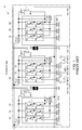
- Fig. 6 is a circuit diagram of a current unbalance detection circuit 504 and a peripheral interface controller (PIC) 506 of a power conversion module 502 that may be used with power conversion system 500.
- current unbalance detection circuit 504 includes a conditioning stage 602, an averaging stage 604, and a difference stage 606.
- the arrangement of components in current unbalance detection circuit 504 is merely exemplary. Accordingly, in other embodiments, current unbalance detection circuit 504 may have any components and/or configuration that enables current unbalance detection circuit 504 to function as described herein.
- conditioning stage 602 receives a module output current, I m .
- the module output current I m is channeled through a first resistor 610 that is electrically coupled to a negative input 612 of a first amplifier 614.
- a positive input 616 of first amplifier 614 is electrically coupled to ground 618.
- Conditioning stage 602 further includes a second resistor 620 coupled to an output 632 of first amplifier 614, and from there, to a positive input 622 of a second amplifier 624.
- Conditioning stage 602 facilitates conditioning the module output current I m for use by averaging stage 604 and difference stage 606.
- conditioning stage 602 may convert a current signal (such as that from a current transformer) into a voltage signal, scale the voltage signal to a desired range that is manageable by an amplifier circuit and/or acquired through A/D channels, and/or introduce filtering to mitigate noise captured by the current transducer.
- a current signal such as that from a current transformer
- Averaging stage 604 includes a third resistor 630 electrically coupled between output 632 of first amplifier 614 and an analog switch 634.
- Analog switch 634 selectively controls whether third resistor 630 is electrically coupled to a positive input 640 of a third amplifier 642.
- PIC 506 controls whether analog switch 634 is open or closed.
- averaging stage 604 receives a reference current, I ref , from other power conversion modules 502 or provides the reference current I ref , to other power conversion modules 502, as described herein.
- Difference stage 606 includes second amplifier 624 and third amplifier 642.
- a negative input 644 of second amplifier 624 is electrically coupled to an output 646 of second amplifier 624
- a negative input 648 of third amplifier 642 is electrically coupled to an output 650 of third amplifier 642.
- a fourth resistor 652 is electrically coupled between output 650 of third amplifier 642 and a negative input 656 of a fourth amplifier 658
- a fifth resistor 660 is electrically coupled between output 646 of second amplifier 624 and a positive input 664 of fourth amplifier 658.
- a sixth resistor 670 is electrically coupled between negative input 656 of fourth amplifier 658 and an output 672 of fourth amplifier 658
- a seventh resistor 674 is electrically coupled between positive input 664 of fourth amplifier 658 and ground 618.
- system 500 includes a plurality of power conversion modules 502.
- analog switches 634 for all power conversion modules 502 are closed
- current unbalance detection circuit 504 for a particular module 502 computes an average of the module output currents I m as the reference current I ref , and computes a difference (i.e., I err ) between the average and the module output current I m for the particular module 502.
- the reference current I ref is the module output current I m for the one module
- current unbalance detection circuit 504 for a particular module 502 computes a difference (i.e., I err ) between the reference current I ref and the module output current I m for the particular module 502.
- any combination of analog switches 634 may be selectively closed to generate different reference currents I ref .
- Analog switches 634 are controlled by PIC 506, which is in turn controlled by main control logic 508 (shown in Fig. 5 ) in the exemplary embodiment. Specifically, each PIC 506 is communicatively coupled to main control logic 508 and PICs 506 of other power conversion modules 502 via a communication bus 680.
- Communication bus 680 may be, for example, a controller area network (CAN).
- the computed difference, I err may be output to PIC 506 for further processing.
- PIC 506 compares the computed difference to a predetermined threshold, and calculates a percentage of time (e.g., of a duty cycle) during which the computed difference exceeds the predefined threshold.
- Fig. 7 is a graph 700 illustrating this comparison over a sample period at 50Hz.
- a central sinewave 702 represents the reference current signals which may be represented as Asin( ⁇ t).
- a currently unbalance threshold, AT can then be defined, resulting in two curves 704 and 706 corresponding to Asin( ⁇ t) ⁇ AT.
- An additional sinewave 708 is the module current, and can be represented as Bsin( ⁇ t).
- main control logic 508 may trigger an alarm and/or take appropriate action (e.g., de-rating the power conversion module 502 in which the current unbalance condition occurs).
- main control logic 508 may trigger an alarm and/or take appropriate action (e.g., de-rating the power conversion module 502 in which the current unbalance condition occurs).
- the embodiments described herein are relatively simple and cost-effective, as they utilize low-performing distributed programmable logic in PICs 506. Although each power conversion module 502 includes a current unbalance detection circuit 504, these are only connected locally and do not contribute to cabling complexity of the overall system 500.
- the embodiments described herein also facilitate improving system reliability by providing a detection of a current unbalance condition. This translates into a commercial advantage over at least some known power conversion systems, as it yields a smarter and more reliable system. Additionally, following the flexibility of detection, this feature is helpful during production testing to assess current unbalance in newly produced units. At the same time, it also facilitates troubleshooting and commissioning field units (i.e., assessing current unbalance in field installations).
- main control logic 508 may select a specific power conversion module 502 to be actively driven (and with current sensing enabled through current unbalance detection circuit 504) while other power conversion modules 502 are maintained in an OFF state. This allows isolating a failed module during troubleshooting. Further, on some embodiments, even sub-sections within a particular power conversion module 502 may be selectively activated and/or deactivated. For example, in a multi-phase converter, each converter leg/phase may be activated separately for additional flexibility during troubleshooting.
- FIG. 8 is a schematic diagram of an exemplary redundant isolated-parallel (IP) uninterruptible power supply (UPS) system 1000.
- system 1000 includes a plurality of UPSs 1002 arranged in a ring architecture, or parallel architecture, as described herein.
- system 1000 includes a first UPS 1004, a second UPS 1006, a third UPS 1008, and a fourth UPS 1010 in the exemplary embodiment.
- system 1000 may include any number of UPSs 1002 that enable system 1000 to function as described herein.
- system 1000 is a three wire system.
- system 1000 may be a four wire system (i.e., a system including a neutral wire to each load).
- UPSs 1002 may be implemented using system 500 and power conversion modules 502 (both shown in Fig. 5 ).
- UPSs 1002 are static double conversion UPSs (i.e., true on-line system systems). Both static and rotary UPSs may require droop control techniques for both voltage and frequency. In some cases, droop control for frequency alone may be sufficient. In some embodiments, droop control techniques are adapted depending on whether a load is linear or non-linear.
- System 1000 facilitates providing power to one or more loads 1020.
- one or more utilities 1022 function as a power source and provide power to loads 1020.
- Utilities 1022 may provide alternating current (AC) or direct current (DC) power to system 1000.
- AC alternating current
- DC direct current
- system 1000 utilizes UPSs 1002 to keep power flowing to loads 1020, as described herein.
- system 1000 includes a first load 1024, a second load 1026, a third load 1028, and a fourth load 1030.
- system 1000 may include any number of loads 1020 that enable system 1000 to function as described herein.
- Each load 1020 is electrically coupled between an associated UPS 1002 and a ring bus 1032.
- each load 1020 is coupled to ring bus 1032 via an associated load circuit breaker 1034.
- ring bus 1032 includes a plurality of ring bus circuit breakers 1036.
- loads 1020 may be coupled directly to ring bus 1032 or may be coupled between UPSs 1002.
- system 1000 may include additional UPSs 1038 coupled directly to ring bus 1032.
- each UPS 1002 is electrically coupled between an input switchgear 1040 and an output switchgear 1042.
- Input switchgears 1040 are electrically coupled to paralleling switchgears 1044, which are in turn electrically coupled to utility 1022 through an associated transformer 1046.
- each paralleling switchgear 1044 is also electrically coupled to one or more grounds 1048.
- Switchgears 1040, 1042, and 1044 include may include local circuits, remote synchronization circuits, and/or software to facilitate attenuating disturbances, interference, and/or crosstalk on ring bus 1032 to provide clean power to loads 1020.
- each output switchgear 1042 is electrically coupled directly to an associated load 1020, and coupled to ring bus 1032 through an associated choke 1050 (e.g., an inductor).
- UPSs 1002 may interfere with one another and/or start to override one another, causing oscillations or other undesirable effects.
- a controller (not shown in Fig. 8 ) controls operation of UPSs 1002. More specifically, the controller controls a frequency of an output voltage of each UPS 1002, as described herein. The frequency for each UPS 1002 is calculated as a function of power, as described herein.
- Fig. 9 is a simplified diagram of system 1000.
- a controller 2000 is communicatively coupled to each of first UPS 1004, second UPS 1006, third UPS 1008, and fourth UPS 1010.
- Controller 2000 may include its own power system (not shown) such as a dedicated energy source (e.g., a battery).
- controller 2000 is coupled to a substitute controller (not shown) that may be used in the event that controller 2000 fails. Controller 2000 may control power distribution and management of system 1000 over a relatively large geographic area.
- controller 2000 is implemented by a processor 2002 communicatively coupled to a memory device 2004 for executing instructions.
- executable instructions are stored in memory device 2004.
- controller 2000 may be implemented using any circuitry that enables controller 2000 to control operation of UPSs 1002 as described herein.
- controller 2000 may include a state machine that learns or is pre-programmed to determine information relevant to which loads 1020 require power. For example, controller 2000 may dynamically determine what power resources will be needed and at what performance level and environmental conditions (e.g., temperature, humidity, time of day, etc.) those power resources will need to operate.
- Controller 2000 may perform dynamic monitoring to determine whether a given load 1020 is satisfied with the power delivered, and whether delivered power is free of harmonics, transients, etc.
- dynamic monitoring may include tracking resource usage to determine how much current or voltage should be delivered.
- Controller 2000 may also monitor and/or control rapidity (i.e., bandwidth) and inverter capability (e.g., overload, reactive power, active power) to facilitate ensuring reliability of system 1000 and minimizing performance degradation of UPSs 1002.
- Controller 2000 may also include a state machine scheduler configured to selectively activate and deactivate power resources, set voltage and current levels, and/or take power saving actions (e.g., reducing current delivery). Controller 2000 may also track characteristics (e.g., static allocation of power) of system 1000 to determine whether one or more components of system 1000 should be put on standby or whether power should be diverted.
- a state machine scheduler configured to selectively activate and deactivate power resources, set voltage and current levels, and/or take power saving actions (e.g., reducing current delivery). Controller 2000 may also track characteristics (e.g., static allocation of power) of system 1000 to determine whether one or more components of system 1000 should be put on standby or whether power should be diverted.
- controller 2000 performs one or more operations described herein by programming processor 2002.
- processor 2002 may be programmed by encoding an operation as one or more executable instructions and by providing the executable instructions in memory device 2004.
- Processor 2002 may include one or more processing units (e.g., in a multi-core configuration). Further, processor 2002 may be implemented using one or more heterogeneous processor systems in which a main processor is present with secondary processors on a single chip. As another illustrative example, processor 2002 may be a symmetric multiprocessor system containing multiple processors of the same type.
- processor 2002 may be implemented using any suitable programmable circuit including one or more systems and microcontrollers, microprocessors, reduced instruction set circuits (RISC), application specific integrated circuits (ASIC), programmable logic circuits, field programmable gate arrays (FPGA), and any other circuit capable of executing the functions described herein.
- processor 2002 causes controller 2000 to operate UPSs 1002, as described herein.
- memory device 2004 is one or more devices that enable information such as executable instructions and/or other data to be stored and retrieved.
- Memory device 2004 may include one or more computer readable media, such as, without limitation, dynamic random access memory (DRAM), static random access memory (SRAM), a solid state disk, and/or a hard disk.
- Memory device 2004 may be configured to store, without limitation, application source code, application object code, source code portions of interest, object code portions of interest, configuration data, execution events and/or any other type of data.
- Main controller logic 508 and/or PICs 506 may be similarly implemented using an associated processor and memory device.
- UPSs 1002 and loads 1020 are electrically coupled to one another through chokes 1050 and ring bus 1032. Further, in the exemplary embodiment, a switch (shown in a closed state in Fig. 9 ) is coupled between each choke 1050 and ring bus 1032.
- Each UPS 1002 includes a rectifier 2006, a DC capacitor 2008, and an inverter 2010 in the exemplary embodiment. Further, each load 1020 is electrically coupled in parallel with an output capacitor (not shown), and each UPS 1002 is electrically coupled in series with an inductor (not shown), in the exemplary embodiment.
- Each inductor and an associated output capacitor form an LC filter, and the phase angle ⁇ is a phase angle of the output voltage of a UPS 1002 as measured across the output capacitor.
- a bypass switch 2012 is coupled in parallel with each choke 1050. Closing bypass switch 2012 causes power flow to bypass an associated choke 1050.
- Loads 1020 can receive power from a local UPS 1002 (e.g., first load 1024 receiving power from first UPS 1004) and from other UPSs 1002 through choke 1050. Accordingly, in the event that a local UPS 1002 fails, a load 1020 can receive power from other UPSs 1002.
- the implementations described herein relate to advanced diagnostics in modular power converters. Specifically, the embodiments described herein build upon a relatively simple modular implementation, where converter modules are paralleled by series impedance while sharing the same PWM modulation. By introducing relatively low-cost local programmable devices at the module level, the systems and methods described herein introduce current unbalance detection in a single-wire implementation, thereby preserving the simplicity of the implementation. When a current unbalance is detected, the systems and methods described herein facilitate alerting a user and permitting investigation and maintenance to prevent module failure.
- An exemplary technical effect of the methods and systems described herein includes at least one of: (a) coupling a plurality of power conversion modules in parallel, wherein all power conversion modules of the plurality of power conversion modules are configured to receive a pulse-width modulation control signal, and (b) calculating, at each power conversion module of the plurality of power conversion modules, a difference between a reference current and an output current of the power conversion module.
Landscapes
- Engineering & Computer Science (AREA)
- Power Engineering (AREA)
- Physics & Mathematics (AREA)
- Electromagnetism (AREA)
- General Physics & Mathematics (AREA)
- Radar, Positioning & Navigation (AREA)
- Automation & Control Theory (AREA)
- Inverter Devices (AREA)
- Dc-Dc Converters (AREA)
Applications Claiming Priority (2)
| Application Number | Priority Date | Filing Date | Title |
|---|---|---|---|
| US201462031913P | 2014-08-01 | 2014-08-01 | |
| US14/556,519 US9857812B2 (en) | 2014-08-01 | 2014-12-01 | Systems and methods for advanced diagnostic in modular power converters |
Publications (2)
| Publication Number | Publication Date |
|---|---|
| EP2980975A1 true EP2980975A1 (de) | 2016-02-03 |
| EP2980975B1 EP2980975B1 (de) | 2023-04-19 |
Family
ID=53682579
Family Applications (1)
| Application Number | Title | Priority Date | Filing Date |
|---|---|---|---|
| EP15177664.8A Active EP2980975B1 (de) | 2014-08-01 | 2015-07-21 | Systeme und verfahren zur erweiterten diagnose in modularen leistungswandlern |
Country Status (4)
| Country | Link |
|---|---|
| US (1) | US9857812B2 (de) |
| EP (1) | EP2980975B1 (de) |
| CN (1) | CN105305786B (de) |
| ES (1) | ES2945329T3 (de) |
Families Citing this family (11)
| Publication number | Priority date | Publication date | Assignee | Title |
|---|---|---|---|---|
| US9780646B2 (en) * | 2015-03-24 | 2017-10-03 | Marotta Controls, Inc. | Switch mode power converter for three phase power |
| KR102606225B1 (ko) | 2016-07-18 | 2023-11-23 | 삼성전자주식회사 | 전원 공급 시스템 |
| JP7144862B2 (ja) * | 2017-04-12 | 2022-09-30 | 国立大学法人京都大学 | スイッチング電源システム、コントローラ、及び制御方法 |
| CN109742934B (zh) * | 2019-01-22 | 2020-09-25 | 江苏建筑职业技术学院 | 一种基于双调制波的功率器件开路故障容错控制方法 |
| EP3916990B1 (de) | 2020-05-28 | 2026-04-15 | Goodrich Control Systems | Verteilte steuerungsarchitektur für motorantriebe |
| EP4024649A1 (de) | 2020-12-29 | 2022-07-06 | Goodrich Control Systems | Verteilte steuerungsarchitektur für motorantriebe |
| EP4044424B1 (de) | 2021-02-12 | 2026-04-01 | Collins Aerospace Ireland, Limited | Strukturen zur steuerung von einzelereignisverzerrungen für parallel antriebssteuerungsarchitekturen von motoren |
| CN112886794B (zh) * | 2021-04-02 | 2024-04-09 | 江西力源海纳科技股份有限公司 | 大功率高频开关电源的控制方法及控制装置 |
| JP7200398B1 (ja) * | 2021-04-16 | 2023-01-06 | 東芝三菱電機産業システム株式会社 | 無停電電源装置 |
| EP4325712A1 (de) | 2022-08-16 | 2024-02-21 | Raytheon Technologies Research Centre Ireland, Limited | Steuerungsstrukturen für parallele motorantriebssteuerungsarchitekturen |
| JP7666770B1 (ja) * | 2025-02-04 | 2025-04-22 | 富士電機株式会社 | 電源システム、制御装置、制御方法 |
Citations (5)
| Publication number | Priority date | Publication date | Assignee | Title |
|---|---|---|---|---|
| EP0813292A2 (de) * | 1996-06-12 | 1997-12-17 | Kabushiki Kaisha Meidensha | Stromwechselrichter mit mindestens drei parallelgesteuerten Stromwechselrichtereinheiten vom PWM Typus |
| US20030161167A1 (en) * | 2002-02-28 | 2003-08-28 | Barnett Rick L. | Interleaved converter power factor correction method and apparatus |
| US20030173937A1 (en) * | 2002-03-15 | 2003-09-18 | Tdk Corporation | Switching power supply control circuit and switching power supply using same |
| EP1850469A1 (de) * | 2005-02-18 | 2007-10-31 | Mitsubishi Denki Kabushiki Kaisha | Wandler-steuervorrichtung |
| JP5112111B2 (ja) * | 2008-03-04 | 2013-01-09 | 株式会社ダイヘン | 直流電源装置、およびこの直流電源装置を用いた系統連系インバータシステム |
Family Cites Families (22)
| Publication number | Priority date | Publication date | Assignee | Title |
|---|---|---|---|---|
| US4276590A (en) | 1979-04-30 | 1981-06-30 | The Perkin-Elmer Corporation | Current sharing modular power system |
| US4924170A (en) | 1989-01-03 | 1990-05-08 | Unisys Corporation | Current sharing modular power supply |
| US5036452A (en) | 1989-12-28 | 1991-07-30 | At&T Bell Laboratories | Current sharing control with limited output voltage range for paralleled power converters |
| US5164890A (en) | 1990-03-29 | 1992-11-17 | Hughes Aircraft Company | Current share scheme for parallel operation of power conditioners |
| US5905645A (en) | 1996-12-02 | 1999-05-18 | Astec International Limited | Thermally aided power sharing of power supplies with or without an external current share line |
| DE69919683D1 (de) | 1999-06-07 | 2004-09-30 | St Microelectronics Srl | Einzeldraht-Stromverteilungssteuerungsverfahren für Parallel-/Redundant Betrieb einer Mehrzahl von Impulsbreitenmodulationskonvertern |
| US6278263B1 (en) | 1999-09-01 | 2001-08-21 | Intersil Corporation | Multi-phase converter with balanced currents |
| US6642631B1 (en) | 2000-10-17 | 2003-11-04 | Semiconductor Components Industries Llc | Circuit and method of direct duty cycle current sharing |
| US20090009005A1 (en) * | 2003-10-02 | 2009-01-08 | Phoenixtec Power Co., Ltd. | Control method for parallel redundant power system |
| US7323794B2 (en) | 2004-11-12 | 2008-01-29 | Dell Products L.P. | Independent control of output current balance between paralleled power units |
| US7170180B2 (en) | 2004-12-20 | 2007-01-30 | General Electric Company | Methods and systems for improved current sharing between parallel power semiconductors in power converters |
| JP4538349B2 (ja) * | 2005-03-17 | 2010-09-08 | 富士通株式会社 | 電源装置および電源システム |
| JP4751810B2 (ja) | 2006-11-02 | 2011-08-17 | 日立オートモティブシステムズ株式会社 | 電力変換装置 |
| US8144489B2 (en) | 2006-12-08 | 2012-03-27 | Siemens Aktiengesellschaft | Production of a real power equilibrium of the phase modules of a converter |
| CN102522896B (zh) * | 2008-04-02 | 2014-11-19 | 台达电子工业股份有限公司 | 并联连接的谐振转换器电路及其控制方法 |
| US8237423B2 (en) | 2008-07-18 | 2012-08-07 | Intersil Americas Inc. | Active droop current sharing |
| TW201007422A (en) * | 2008-08-05 | 2010-02-16 | Richtek Technology Corp | Multi-functional drMOS |
| US7940537B2 (en) | 2008-12-31 | 2011-05-10 | Teco-Westinghouse Motor Company | Partial regeneration in a multi-level power inverter |
| US8552589B2 (en) * | 2010-05-14 | 2013-10-08 | Schneider Electric It Corporation | Digital control method for operating the UPS systems in parallel |
| US8536842B2 (en) * | 2011-03-03 | 2013-09-17 | Exar Corporation | Sensorless self-tuning digital current programmed mode (CPM) controller with multiple parameter estimation and thermal stress equalization |
| US8630103B2 (en) | 2011-06-15 | 2014-01-14 | Power Integrations, Inc. | Method and apparatus for programming a power converter controller with an external programming terminal having multiple functions |
| KR101584057B1 (ko) | 2012-07-06 | 2016-01-22 | 에이비비 테크놀로지 아게 | 모듈러 컨버터 제어 |
-
2014
- 2014-12-01 US US14/556,519 patent/US9857812B2/en active Active
-
2015
- 2015-07-21 EP EP15177664.8A patent/EP2980975B1/de active Active
- 2015-07-21 ES ES15177664T patent/ES2945329T3/es active Active
- 2015-07-31 CN CN201510461393.0A patent/CN105305786B/zh active Active
Patent Citations (5)
| Publication number | Priority date | Publication date | Assignee | Title |
|---|---|---|---|---|
| EP0813292A2 (de) * | 1996-06-12 | 1997-12-17 | Kabushiki Kaisha Meidensha | Stromwechselrichter mit mindestens drei parallelgesteuerten Stromwechselrichtereinheiten vom PWM Typus |
| US20030161167A1 (en) * | 2002-02-28 | 2003-08-28 | Barnett Rick L. | Interleaved converter power factor correction method and apparatus |
| US20030173937A1 (en) * | 2002-03-15 | 2003-09-18 | Tdk Corporation | Switching power supply control circuit and switching power supply using same |
| EP1850469A1 (de) * | 2005-02-18 | 2007-10-31 | Mitsubishi Denki Kabushiki Kaisha | Wandler-steuervorrichtung |
| JP5112111B2 (ja) * | 2008-03-04 | 2013-01-09 | 株式会社ダイヘン | 直流電源装置、およびこの直流電源装置を用いた系統連系インバータシステム |
Also Published As
| Publication number | Publication date |
|---|---|
| US9857812B2 (en) | 2018-01-02 |
| CN105305786A (zh) | 2016-02-03 |
| CN105305786B (zh) | 2019-09-24 |
| EP2980975B1 (de) | 2023-04-19 |
| ES2945329T3 (es) | 2023-06-30 |
| US20160033978A1 (en) | 2016-02-04 |
Similar Documents
| Publication | Publication Date | Title |
|---|---|---|
| US9857812B2 (en) | Systems and methods for advanced diagnostic in modular power converters | |
| CN107819357B (zh) | 带有故障位置检测的隔离并联ups系统 | |
| US9705360B2 (en) | Redundant uninterruptible power supply systems | |
| Ghazanfari et al. | A resilient framework for fault-tolerant operation of modular multilevel converters | |
| CN107819356B (zh) | 带有扼流圈旁路开关的隔离并联不间断电源系统 | |
| JP6357679B2 (ja) | 地絡検出のための方法および装置 | |
| Xue et al. | Smart inverters for utility and industry applications | |
| US8816533B2 (en) | Uninterruptible power supply systems and methods using an isolated neutral reference | |
| JP5645864B2 (ja) | 三相不平衡抑制システム | |
| US9882424B2 (en) | Redundant uninterruptible power supply systems | |
| CN105305532B (zh) | 用于管理不间断电源系统中的反向馈电的系统和方法 | |
| CN105720677B (zh) | 用于实现在静态ups中的串联补偿器的系统和方法 | |
| US20130258718A1 (en) | System, method, and apparatus for powering equipment during a low voltage event | |
| KR102805667B1 (ko) | 그리드 아일랜딩 검출 방법 및 장치 | |
| US10031168B2 (en) | Detection of islanding condition in electricity network | |
| Lin et al. | Modular power architectures for microgrid clusters | |
| JP2015107033A (ja) | 解列制御装置、解列制御方法およびパワーコンディショナー | |
| WO2023095256A1 (ja) | 無停電電源装置 |
Legal Events
| Date | Code | Title | Description |
|---|---|---|---|
| PUAI | Public reference made under article 153(3) epc to a published international application that has entered the european phase |
Free format text: ORIGINAL CODE: 0009012 |
|
| AK | Designated contracting states |
Kind code of ref document: A1 Designated state(s): AL AT BE BG CH CY CZ DE DK EE ES FI FR GB GR HR HU IE IS IT LI LT LU LV MC MK MT NL NO PL PT RO RS SE SI SK SM TR |
|
| AX | Request for extension of the european patent |
Extension state: BA ME |
|
| 17P | Request for examination filed |
Effective date: 20160803 |
|
| RBV | Designated contracting states (corrected) |
Designated state(s): AL AT BE BG CH CY CZ DE DK EE ES FI FR GB GR HR HU IE IS IT LI LT LU LV MC MK MT NL NO PL PT RO RS SE SI SK SM TR |
|
| STAA | Information on the status of an ep patent application or granted ep patent |
Free format text: STATUS: EXAMINATION IS IN PROGRESS |
|
| 17Q | First examination report despatched |
Effective date: 20170926 |
|
| RAP1 | Party data changed (applicant data changed or rights of an application transferred) |
Owner name: ABB SCHWEIZ AG |
|
| RAP3 | Party data changed (applicant data changed or rights of an application transferred) |
Owner name: ABB SCHWEIZ AG |
|
| GRAP | Despatch of communication of intention to grant a patent |
Free format text: ORIGINAL CODE: EPIDOSNIGR1 |
|
| STAA | Information on the status of an ep patent application or granted ep patent |
Free format text: STATUS: GRANT OF PATENT IS INTENDED |
|
| INTG | Intention to grant announced |
Effective date: 20221208 |
|
| GRAS | Grant fee paid |
Free format text: ORIGINAL CODE: EPIDOSNIGR3 |
|
| GRAA | (expected) grant |
Free format text: ORIGINAL CODE: 0009210 |
|
| STAA | Information on the status of an ep patent application or granted ep patent |
Free format text: STATUS: THE PATENT HAS BEEN GRANTED |
|
| AK | Designated contracting states |
Kind code of ref document: B1 Designated state(s): AL AT BE BG CH CY CZ DE DK EE ES FI FR GB GR HR HU IE IS IT LI LT LU LV MC MK MT NL NO PL PT RO RS SE SI SK SM TR |
|
| REG | Reference to a national code |
Ref country code: GB Ref legal event code: FG4D |
|
| REG | Reference to a national code |
Ref country code: DE Ref legal event code: R096 Ref document number: 602015083200 Country of ref document: DE |
|
| REG | Reference to a national code |
Ref country code: CH Ref legal event code: EP |
|
| REG | Reference to a national code |
Ref country code: IE Ref legal event code: FG4D |
|
| REG | Reference to a national code |
Ref country code: AT Ref legal event code: REF Ref document number: 1561942 Country of ref document: AT Kind code of ref document: T Effective date: 20230515 |
|
| REG | Reference to a national code |
Ref country code: ES Ref legal event code: FG2A Ref document number: 2945329 Country of ref document: ES Kind code of ref document: T3 Effective date: 20230630 |
|
| REG | Reference to a national code |
Ref country code: LT Ref legal event code: MG9D |
|
| REG | Reference to a national code |
Ref country code: NL Ref legal event code: MP Effective date: 20230419 |
|
| REG | Reference to a national code |
Ref country code: AT Ref legal event code: MK05 Ref document number: 1561942 Country of ref document: AT Kind code of ref document: T Effective date: 20230419 |
|
| PG25 | Lapsed in a contracting state [announced via postgrant information from national office to epo] |
Ref country code: NL Free format text: LAPSE BECAUSE OF FAILURE TO SUBMIT A TRANSLATION OF THE DESCRIPTION OR TO PAY THE FEE WITHIN THE PRESCRIBED TIME-LIMIT Effective date: 20230419 |
|
| PG25 | Lapsed in a contracting state [announced via postgrant information from national office to epo] |
Ref country code: SE Free format text: LAPSE BECAUSE OF FAILURE TO SUBMIT A TRANSLATION OF THE DESCRIPTION OR TO PAY THE FEE WITHIN THE PRESCRIBED TIME-LIMIT Effective date: 20230419 Ref country code: PT Free format text: LAPSE BECAUSE OF FAILURE TO SUBMIT A TRANSLATION OF THE DESCRIPTION OR TO PAY THE FEE WITHIN THE PRESCRIBED TIME-LIMIT Effective date: 20230821 Ref country code: NO Free format text: LAPSE BECAUSE OF FAILURE TO SUBMIT A TRANSLATION OF THE DESCRIPTION OR TO PAY THE FEE WITHIN THE PRESCRIBED TIME-LIMIT Effective date: 20230719 Ref country code: AT Free format text: LAPSE BECAUSE OF FAILURE TO SUBMIT A TRANSLATION OF THE DESCRIPTION OR TO PAY THE FEE WITHIN THE PRESCRIBED TIME-LIMIT Effective date: 20230419 |
|
| PG25 | Lapsed in a contracting state [announced via postgrant information from national office to epo] |
Ref country code: RS Free format text: LAPSE BECAUSE OF FAILURE TO SUBMIT A TRANSLATION OF THE DESCRIPTION OR TO PAY THE FEE WITHIN THE PRESCRIBED TIME-LIMIT Effective date: 20230419 Ref country code: PL Free format text: LAPSE BECAUSE OF FAILURE TO SUBMIT A TRANSLATION OF THE DESCRIPTION OR TO PAY THE FEE WITHIN THE PRESCRIBED TIME-LIMIT Effective date: 20230419 Ref country code: LV Free format text: LAPSE BECAUSE OF FAILURE TO SUBMIT A TRANSLATION OF THE DESCRIPTION OR TO PAY THE FEE WITHIN THE PRESCRIBED TIME-LIMIT Effective date: 20230419 Ref country code: LT Free format text: LAPSE BECAUSE OF FAILURE TO SUBMIT A TRANSLATION OF THE DESCRIPTION OR TO PAY THE FEE WITHIN THE PRESCRIBED TIME-LIMIT Effective date: 20230419 Ref country code: IS Free format text: LAPSE BECAUSE OF FAILURE TO SUBMIT A TRANSLATION OF THE DESCRIPTION OR TO PAY THE FEE WITHIN THE PRESCRIBED TIME-LIMIT Effective date: 20230819 Ref country code: HR Free format text: LAPSE BECAUSE OF FAILURE TO SUBMIT A TRANSLATION OF THE DESCRIPTION OR TO PAY THE FEE WITHIN THE PRESCRIBED TIME-LIMIT Effective date: 20230419 Ref country code: GR Free format text: LAPSE BECAUSE OF FAILURE TO SUBMIT A TRANSLATION OF THE DESCRIPTION OR TO PAY THE FEE WITHIN THE PRESCRIBED TIME-LIMIT Effective date: 20230720 Ref country code: AL Free format text: LAPSE BECAUSE OF FAILURE TO SUBMIT A TRANSLATION OF THE DESCRIPTION OR TO PAY THE FEE WITHIN THE PRESCRIBED TIME-LIMIT Effective date: 20230419 |
|
| PG25 | Lapsed in a contracting state [announced via postgrant information from national office to epo] |
Ref country code: FI Free format text: LAPSE BECAUSE OF FAILURE TO SUBMIT A TRANSLATION OF THE DESCRIPTION OR TO PAY THE FEE WITHIN THE PRESCRIBED TIME-LIMIT Effective date: 20230419 |
|
| PG25 | Lapsed in a contracting state [announced via postgrant information from national office to epo] |
Ref country code: SK Free format text: LAPSE BECAUSE OF FAILURE TO SUBMIT A TRANSLATION OF THE DESCRIPTION OR TO PAY THE FEE WITHIN THE PRESCRIBED TIME-LIMIT Effective date: 20230419 |
|
| REG | Reference to a national code |
Ref country code: DE Ref legal event code: R097 Ref document number: 602015083200 Country of ref document: DE |
|
| PG25 | Lapsed in a contracting state [announced via postgrant information from national office to epo] |
Ref country code: SM Free format text: LAPSE BECAUSE OF FAILURE TO SUBMIT A TRANSLATION OF THE DESCRIPTION OR TO PAY THE FEE WITHIN THE PRESCRIBED TIME-LIMIT Effective date: 20230419 Ref country code: SK Free format text: LAPSE BECAUSE OF FAILURE TO SUBMIT A TRANSLATION OF THE DESCRIPTION OR TO PAY THE FEE WITHIN THE PRESCRIBED TIME-LIMIT Effective date: 20230419 Ref country code: RO Free format text: LAPSE BECAUSE OF FAILURE TO SUBMIT A TRANSLATION OF THE DESCRIPTION OR TO PAY THE FEE WITHIN THE PRESCRIBED TIME-LIMIT Effective date: 20230419 Ref country code: EE Free format text: LAPSE BECAUSE OF FAILURE TO SUBMIT A TRANSLATION OF THE DESCRIPTION OR TO PAY THE FEE WITHIN THE PRESCRIBED TIME-LIMIT Effective date: 20230419 Ref country code: DK Free format text: LAPSE BECAUSE OF FAILURE TO SUBMIT A TRANSLATION OF THE DESCRIPTION OR TO PAY THE FEE WITHIN THE PRESCRIBED TIME-LIMIT Effective date: 20230419 Ref country code: CZ Free format text: LAPSE BECAUSE OF FAILURE TO SUBMIT A TRANSLATION OF THE DESCRIPTION OR TO PAY THE FEE WITHIN THE PRESCRIBED TIME-LIMIT Effective date: 20230419 |
|
| PLBE | No opposition filed within time limit |
Free format text: ORIGINAL CODE: 0009261 |
|
| STAA | Information on the status of an ep patent application or granted ep patent |
Free format text: STATUS: NO OPPOSITION FILED WITHIN TIME LIMIT |
|
| PG25 | Lapsed in a contracting state [announced via postgrant information from national office to epo] |
Ref country code: MC Free format text: LAPSE BECAUSE OF FAILURE TO SUBMIT A TRANSLATION OF THE DESCRIPTION OR TO PAY THE FEE WITHIN THE PRESCRIBED TIME-LIMIT Effective date: 20230419 |
|
| PG25 | Lapsed in a contracting state [announced via postgrant information from national office to epo] |
Ref country code: MC Free format text: LAPSE BECAUSE OF FAILURE TO SUBMIT A TRANSLATION OF THE DESCRIPTION OR TO PAY THE FEE WITHIN THE PRESCRIBED TIME-LIMIT Effective date: 20230419 |
|
| REG | Reference to a national code |
Ref country code: BE Ref legal event code: MM Effective date: 20230731 |
|
| PG25 | Lapsed in a contracting state [announced via postgrant information from national office to epo] |
Ref country code: LU Free format text: LAPSE BECAUSE OF NON-PAYMENT OF DUE FEES Effective date: 20230721 |
|
| 26N | No opposition filed |
Effective date: 20240122 |
|
| PG25 | Lapsed in a contracting state [announced via postgrant information from national office to epo] |
Ref country code: LU Free format text: LAPSE BECAUSE OF NON-PAYMENT OF DUE FEES Effective date: 20230721 |
|
| REG | Reference to a national code |
Ref country code: IE Ref legal event code: MM4A |
|
| PG25 | Lapsed in a contracting state [announced via postgrant information from national office to epo] |
Ref country code: SI Free format text: LAPSE BECAUSE OF FAILURE TO SUBMIT A TRANSLATION OF THE DESCRIPTION OR TO PAY THE FEE WITHIN THE PRESCRIBED TIME-LIMIT Effective date: 20230419 |
|
| PG25 | Lapsed in a contracting state [announced via postgrant information from national office to epo] |
Ref country code: SI Free format text: LAPSE BECAUSE OF FAILURE TO SUBMIT A TRANSLATION OF THE DESCRIPTION OR TO PAY THE FEE WITHIN THE PRESCRIBED TIME-LIMIT Effective date: 20230419 Ref country code: BE Free format text: LAPSE BECAUSE OF NON-PAYMENT OF DUE FEES Effective date: 20230731 |
|
| PG25 | Lapsed in a contracting state [announced via postgrant information from national office to epo] |
Ref country code: IE Free format text: LAPSE BECAUSE OF NON-PAYMENT OF DUE FEES Effective date: 20230721 |
|
| PG25 | Lapsed in a contracting state [announced via postgrant information from national office to epo] |
Ref country code: IE Free format text: LAPSE BECAUSE OF NON-PAYMENT OF DUE FEES Effective date: 20230721 |
|
| PG25 | Lapsed in a contracting state [announced via postgrant information from national office to epo] |
Ref country code: BG Free format text: LAPSE BECAUSE OF FAILURE TO SUBMIT A TRANSLATION OF THE DESCRIPTION OR TO PAY THE FEE WITHIN THE PRESCRIBED TIME-LIMIT Effective date: 20230419 |
|
| PG25 | Lapsed in a contracting state [announced via postgrant information from national office to epo] |
Ref country code: BG Free format text: LAPSE BECAUSE OF FAILURE TO SUBMIT A TRANSLATION OF THE DESCRIPTION OR TO PAY THE FEE WITHIN THE PRESCRIBED TIME-LIMIT Effective date: 20230419 |
|
| PG25 | Lapsed in a contracting state [announced via postgrant information from national office to epo] |
Ref country code: CY Free format text: LAPSE BECAUSE OF FAILURE TO SUBMIT A TRANSLATION OF THE DESCRIPTION OR TO PAY THE FEE WITHIN THE PRESCRIBED TIME-LIMIT; INVALID AB INITIO Effective date: 20150721 |
|
| PG25 | Lapsed in a contracting state [announced via postgrant information from national office to epo] |
Ref country code: HU Free format text: LAPSE BECAUSE OF FAILURE TO SUBMIT A TRANSLATION OF THE DESCRIPTION OR TO PAY THE FEE WITHIN THE PRESCRIBED TIME-LIMIT; INVALID AB INITIO Effective date: 20150721 |
|
| PGFP | Annual fee paid to national office [announced via postgrant information from national office to epo] |
Ref country code: ES Payment date: 20250826 Year of fee payment: 11 |
|
| PGFP | Annual fee paid to national office [announced via postgrant information from national office to epo] |
Ref country code: DE Payment date: 20250722 Year of fee payment: 11 |
|
| PGFP | Annual fee paid to national office [announced via postgrant information from national office to epo] |
Ref country code: IT Payment date: 20250724 Year of fee payment: 11 |
|
| PGFP | Annual fee paid to national office [announced via postgrant information from national office to epo] |
Ref country code: GB Payment date: 20250722 Year of fee payment: 11 |
|
| PGFP | Annual fee paid to national office [announced via postgrant information from national office to epo] |
Ref country code: FR Payment date: 20250725 Year of fee payment: 11 |
|
| PGFP | Annual fee paid to national office [announced via postgrant information from national office to epo] |
Ref country code: CH Payment date: 20250801 Year of fee payment: 11 |
|
| PG25 | Lapsed in a contracting state [announced via postgrant information from national office to epo] |
Ref country code: TR Free format text: LAPSE BECAUSE OF FAILURE TO SUBMIT A TRANSLATION OF THE DESCRIPTION OR TO PAY THE FEE WITHIN THE PRESCRIBED TIME-LIMIT Effective date: 20230419 |