EP2983247B1 - Connecteur enfichable - Google Patents
Connecteur enfichable Download PDFInfo
- Publication number
- EP2983247B1 EP2983247B1 EP15177989.9A EP15177989A EP2983247B1 EP 2983247 B1 EP2983247 B1 EP 2983247B1 EP 15177989 A EP15177989 A EP 15177989A EP 2983247 B1 EP2983247 B1 EP 2983247B1
- Authority
- EP
- European Patent Office
- Prior art keywords
- substrate
- slider
- housing cavity
- contactor
- insulator
- Prior art date
- Legal status (The legal status is an assumption and is not a legal conclusion. Google has not performed a legal analysis and makes no representation as to the accuracy of the status listed.)
- Active
Links
Images




Classifications
-
- H—ELECTRICITY
- H01—ELECTRIC ELEMENTS
- H01R—ELECTRICALLY-CONDUCTIVE CONNECTIONS; STRUCTURAL ASSOCIATIONS OF A PLURALITY OF MUTUALLY-INSULATED ELECTRICAL CONNECTING ELEMENTS; COUPLING DEVICES; CURRENT COLLECTORS
- H01R12/00—Structural associations of a plurality of mutually-insulated electrical connecting elements, specially adapted for printed circuits, e.g. printed circuit boards [PCB], flat or ribbon cables, or like generally planar structures, e.g. terminal strips, terminal blocks; Coupling devices specially adapted for printed circuits, flat or ribbon cables, or like generally planar structures; Terminals specially adapted for contact with, or insertion into, printed circuits, flat or ribbon cables, or like generally planar structures
- H01R12/70—Coupling devices
- H01R12/71—Coupling devices for rigid printing circuits or like structures
- H01R12/72—Coupling devices for rigid printing circuits or like structures coupling with the edge of the rigid printed circuits or like structures
- H01R12/721—Coupling devices for rigid printing circuits or like structures coupling with the edge of the rigid printed circuits or like structures cooperating directly with the edge of the rigid printed circuits
-
- H—ELECTRICITY
- H01—ELECTRIC ELEMENTS
- H01R—ELECTRICALLY-CONDUCTIVE CONNECTIONS; STRUCTURAL ASSOCIATIONS OF A PLURALITY OF MUTUALLY-INSULATED ELECTRICAL CONNECTING ELEMENTS; COUPLING DEVICES; CURRENT COLLECTORS
- H01R12/00—Structural associations of a plurality of mutually-insulated electrical connecting elements, specially adapted for printed circuits, e.g. printed circuit boards [PCB], flat or ribbon cables, or like generally planar structures, e.g. terminal strips, terminal blocks; Coupling devices specially adapted for printed circuits, flat or ribbon cables, or like generally planar structures; Terminals specially adapted for contact with, or insertion into, printed circuits, flat or ribbon cables, or like generally planar structures
- H01R12/70—Coupling devices
- H01R12/82—Coupling devices connected with low or zero insertion force
- H01R12/85—Coupling devices connected with low or zero insertion force contact pressure producing means, contacts activated after insertion of printed circuits or like structures
- H01R12/89—Coupling devices connected with low or zero insertion force contact pressure producing means, contacts activated after insertion of printed circuits or like structures acting manually by moving connector housing parts linearly, e.g. slider
Definitions
- the present invention relates to a plug connector comprising a plurality of contactors.
- a plug connector of a multi-poled zero insertion force (ZIF) connector type has an insulator to which a plurality of contactors is fixed, and a substrate housed inside the insulator.
- the substrate has an electrode pad electrically connected to the contactor.
- a lead contact part of the contactor and the electrode pad of the substrate are soldered to each other, whereby electrical connection is fixed.
- soldering work between the lead contact part of the contactor and the electrode pad of the substrate is generally performed by hand using soldering iron (for example, see Japanese Unexamined Patent Application Publication No. 2002-170645 or Japanese Unexamined Patent Application Publication No. 2014-086187 ).
- a plug connector is a multi-poled type having a plurality of contactors
- a pitch between the contactors becomes narrow.
- a bridge may occur in which the lead contact parts of the contactors adjacent to each other are electrically connected via soldering.
- flux liquid used for soldering work interferes with joints of the lead contact part of the contactor and the electrode pad of the substrate, and consequently, malfunctions may be caused in the electrical connection between the lead contact part and the electrode pad.
- the object of the present invention is to provide a plug connector capable of improving the efficiency of attaching work of the substrates, and improving the yield.
- the present invention solves the above problem with a plug connector according to claim 1.
- a plug connector capable of improving the efficiency of attaching work of the substrates and improved yield is provided.
- FIG. 1 is a perspective view illustrating a plug connector 10.
- the plug connector 10 is used, for example, for connecting electronic devices to each other. More specifically, the plug connector 10 is provided on one electronic device, and is formed attachably and detachably to and from a receptacle connector provided in the other electronic device.
- FIG. 2 is an exploded perspective view illustrating a state where the plug connector 10 is disassembled.
- the plug connector 10 includes a housing shell 20, and a pair of sub-assemblies 30 housed inside the housing shell 20.
- the sub-assemblies 30 each have the similar structure. For this reason, description will be given using the same reference numerals designated to both sub-assemblies.
- the sub-assembly 30 has a substrate 40 provided with a plurality of electrode pads 41, an insulator 50 capable of housing the substrate 40, a plurality of contactors 80 provided inside the insulator 50 and electrically connected to the electrode pads 41 of the substrate 40, and a slider 60 housed inside the insulator 50 and slidably formed relative to the insulator 50.
- a plurality of electrode pads 41 is provided at edge parts along a longitudinal direction of both principal surfaces 42, 43 of the substrate 40.
- the electrode pads 41 are arranged in a row along the longitudinal direction of the substrate 40.
- the substrate 40 is formed to be connectable to the one electronic device described above.
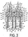
- FIG. 3 is a cross-sectional view illustrating the plug connector 10 along a cross-section orthogonal to a longitudinal direction thereof.
- the insulator 50 is formed of an insulating member. The insulator 50 is formed so as to enable the slider 60 to be housed therein and to be slidable.
- a first housing cavity 51 that can house the slider 60 is formed inside the insulator 50.
- openings 54, 55 communicated with the housing cavity 51 are formed.
- a step part 57 which is the fourth abutting part is formed.
- the step part 57 protrudes toward an inner side of the housing cavity 51, with respect to a range of the step part 57 from the opening 54.
- a width from the opening 54 to the step part 57 in the housing cavity 51, that is, a width between the inner surfaces 56 of the housing cavity 51 is set such that the slider 60 can be housed.
- a width between the step parts 57 is set narrower than a width of the slider 60.
- the slider 60 is housed movably in a range from the opening 54 of the housing cavity 51 of the insulator 50 to the step part 57.
- the slider 60 includes a main body part 61 formed, for example, in a rectangular shape, and a substrate receiver part 62 formed inside the main body part 61.
- the main body part 61 is housed slidably in a range from the opening 54 of the housing cavity 51 of the insulator 50 to the step part 57. More specifically, the main body part 61 is formed, so as to be slidable, such that a width is the same as a length across a range from the opening 54 to the step part 57 in the surface parts 56a, 56b, or is slightly smaller than a length across a range from the opening 54 to the step part 57 in the surface parts 56a, 56b. Both side surfaces opposed to the surface parts 56a, 56b of the housing cavity 51 in the main body part 61 are formed parallel to the surface parts 56a, 56b of the housing cavity 51.
- an engaging hole part 59 that communicates the outside with the housing cavity 51.
- the engaging hole part 59 is formed on the wall part on both sides so as to sandwich the housing cavity 51. Further, as illustrated in FIG. 2 , in the present embodiment, each of the engaging hole parts 59 is formed on each end part along the longitudinal direction of the insulator 50.
- an engaging protruded part (regulating part, first abutting part) 70 that protrudes toward the outside in a width direction.
- the engaging protruded part 70 is formed to be housable in the engaging hole part 59 of the insulator 50.
- the engaging hole part 59 is formed longer than the engaging protruded part 70 along a slide direction of the slider 60 relative to the insulator 50.
- the inner surface (regulating part, second abutting part) 59a of the opening 54 side of the engaging hole part 59 is a plane orthogonal to a moving direction of the slider 60 relative to the insulator 50.
- An end face 71 opposed in the slide direction to the inner surface 59a of the engaging hole part 59 in the engaging protruded part 70 is a plane orthogonal to the slide direction.
- An opposite-side end face 72 of the end face 71 of the engaging protruded part 70 is inclined relative to the slide direction relative to the insulator 50 of the slider 60. This is for the purpose of making the insertion work to be performed easily, when the slider 60 is inserted through the opening 54 into the housing cavity 51 of the insulator 50, from a state where the slider 60 is disassembled with respect to the insulator 50.
- the slider 60 becomes slidable between a first position 90 (illustrated in FIG. 4 described below) where the end face 71 of the engaging protruded part 70 abuts against the inner surface 59a of the engaging hole part 59, and a second position 91 where the slider 60 abuts against the step part 57 of the insulator 50.
- the second housing cavity 65 is formed in the main body part 61 of the slider 60.
- an opening 67 that communicates with the housing cavity 65 is formed on one end face 66 orthogonal to the slide direction of the main body part 61 relative to the insulator 50.
- the opening 69 that communicates with the housing cavity 65 is formed on an end face 68 which is the third abutting part on the opposite side to the end face 66 across the housing cavity 65 in the main body part 61.
- the end face 68 of the main body part 61 is formed abuttably against the step part 57 of the insulator 50.
- a position where the end face 68 abuts against the step part 57 is the second position 91.
- the main body part 61 has a height enough to allow it to extend to the outside through the opening 54 of the insulator 50, in a state where the end face 68 abuts against the step part 57 of the insulator 50.
- the substrate receiver part 62 is housed inside the housing cavity 65 of the main body part 61, and is formed slidably relative to the insulator 50 integral with the main body part 61. Specifically, the substrate receiver part 62 is fixed at both ends in the longitudinal direction of the main body part 61. The substrate receiver part 62 is arranged to have a clearance 93 between both inner surfaces along the longitudinal direction of the housing cavity 65.
- a number of the contactors 80 equal to that of the electrode pads 41 provided on one of the substrates 40 are provided in the housing cavity 51 of the insulator 50. More specifically, in the housing cavity 51 of the insulator 50, a number of the contactors 80 equal to that of the electrode pads 41 provided on one principal surface 42 are provided, on a portion opposed to one principal surface 42 of the substrate 40, that is, a portion along the longitudinal direction of the housing cavity 51. These contactors 80 are arranged spaced apart from one another in a pitch equal to a pitch between the electrode pads 41. These contactors 80 are arranged connectably to the corresponding electrode pads 41.
- the contactors 80 are provided in the other portion along the longitudinal direction of the housing cavity 51 .
- the contactor 80 provided on the one portion along the longitudinal direction of the housing cavity 51, and the contactor 80 provided on the other portion along the longitudinal direction of the housing cavity 51 are provided symmetrically across the substrate receiver part 62.
- plating processing is carried out on the surfaces of the respective contactors 80 using a metal having a high conductivity.
- the contactor 80 has a length extending from one end to the other end in a height direction of the insulator 50, in other words, a length extending from the opening 55 to the opening 54.
- the one end part 81 of the contactor 80 is fixed in the vicinity of the opening 55 of the insulator 50.
- the one end part 81 of the contactor 80 when connected to the receptacle connector described above, is electrically connected to the contactor of the receptacle connector.
- a section from the one end part 81 to the step part 57 is formed parallel to the inner surfaces of the housing cavity 51 of the insulator 50.
- the other end part 82 of the contactor 80 is housed within the housing cavity 65 of the slider 60 through the opening 64 of the slider 60. More specifically, the other end part 82 of the contactor 80 is housed inside the clearance 93 defined between the inner surface of the housing cavity 65 of the slider 60 and the substrate receiver part 62.
- the other end part 82 of the contactors 80 includes a bending part 83 that bends the contactors 80 toward the substrate receiver part 62 side, a protruding part 85 that protrudes toward the inner surface of the housing cavity 65 of the slider 60, a slope 86 inclined toward a width direction inner side of the housing cavity 65 of the slider 60, and a lead contact part 87 formed connectably to the electrode pads 41 of the substrate 40.
- the bending part 83 is opposed in the width direction to the step part 57 of the insulator 50.
- the bending part 83 is bent in the width direction inner side of the housing cavity 65, relative to the section from the one end part 81 to the bending part 83 in the contactor 80.
- the protruding part 85 is formed by curving the contactor 80.
- the protruding part 85 protrudes toward the inner surface of the housing cavity 65 of the slider 60.
- the inner surface of the housing cavity 65 of the slider 60, and the protruding part 85 will be specifically described.
- the pressing stepped part 73 is formed, in a range from a position in the vicinity of the opening 69 to the opening 69.
- the pressing stepped part 73 protrudes toward the width direction inner side of the housing cavity 65.
- the inner surface 74 of the pressing stepped part 73 is parallel to the slide direction of the slider 60 relative to the insulator 50.
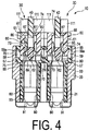
- FIG. 4 is a cross-sectional view illustrating, similar to FIG. 3 , a state where the slider 60 is located at the first position 90, and the substrate 40 is apart from the substrate receiver part 62.
- the pressing stepped part 73 is formed at a position where the pressing stepped part 73 does not abut against the protruding part 85, in a state where the slider 60 is located at the first position 90.
- the inclined plane 75 is formed on the opening 69 side in the pressing stepped part 73.
- the inclined plane 75 is inclined to the slide direction of the slider 60 relative to the insulator 50, and formed so that the protruding part 85 can ride thereon, when the slider 60 moves from the first position 90 to the second position 91.
- the slope part 86 of the contactor 80 is formed continuous to the protruding part 85.
- the lead contact part 87 is formed continuous to the slope part 86.
- the slope part 86 is inclined to the slide direction of the slider 60 relative to the insulator 50. Therefore, the lead contact part 87 is arranged on the width direction inner side of the housing cavity 65, relative to the protruding part 85.
- the slope part 86 will be specifically described. As illustrated in FIG. 4 , the slope part 86 abuts against the substrate receiver part 62, in a state where the slider 60 is located at the first position 90.
- the substrate receiver part 62 is formed by abutting against the slope part 86, so that the position of the lead contact part 87 can be fixed, that is, can be positioned, at a position apart from the trajectory of the substrate 40.
- the trajectory of the substrate 40 is a path along which the substrate 40 moves until the substrate 40 abuts against the substrate receiver part 62, in a range from the opening 67 of the slider 60 to the substrate receiver part 62.
- the position of the lead contact part 87 is fixed at a position apart from the trajectory of the substrate 40, whereby the inserted tip end and the electrode pad 41 of the substrate 40 do not come into contact with the lead contact part 87 of the contactor 80, even when the substrate 40 is housed into the slider 60 through the opening 67, in a state where the slider 60 is located at the first position 90.
- the substrate receiver part 62 comes into contact with the slope part 86, in a state where the slider 60 is located at the first position 90, whereby the lead contact part 87 may be fixed, that is, positioned at a position where a pressing force applied from the lead contact part 87 to the substrate 40 is within a predetermined value.
- the lead contact part 87 By positioning the lead contact part 87 at the position where it comes into contact with the substrate 40, the lead contact part 87 comes into contact with a tip end of the substrate 40 when the substrate 40 is inserted into the slider 60, and rides on the tip end.
- the lead contact part 87 rides on the tip end of the substrate 40, whereby the contactor 80 is deflected. As a result, the lead contact part 87 is pressed against the tip end of the substrate 40 by an elastic force of the contactor 80. The pressing force becomes large in direct proportional to an amount of deflection of the contactor 80.
- the above-described predetermined value is a maximum value of a range within which plating on the surface of the lead contact part 87 is not peeled. In other words, if the predetermined value is exceeded, the plating will be peeled.
- the predetermined value can be obtained by experiment or the like.
- a housing shell 20 is formed to be capable of housing two sub-assemblies 30. Specifically, inside the housing shell 20, a housing cavity or space part 21 is formed. The housing cavity 21 is formed to be capable of housing and fixing two sub-assemblies 30 coupled in the width direction.
- the insulators 50 are fixed to the housing shells 20, for example, by screws 100.
- each insulator 50 there are formed enclosure parts 110 that cover longitudinal both end parts of the substrate 40.
- the shapes of the respective enclosure parts 110 are the same.
- the enclosure part 110 is in a planar shape, which is C-shaped and opened to one side, and has a pair of side walls 111, and an end wall 112 that connects both side walls 111.
- the pair of side walls 111 and the end wall 112 are formed such that the longitudinal end part of the substrate 40 can be fitted thereon, in a range enclosed by these both side walls 111 and the end wall 112.
- engaging hole parts (fixing structures, first engaging parts) 113 that penetrate the both side walls 111 in the width direction are formed.
- engaging groove parts 44 that penetrate the substrates 40 in the width direction are formed at portions opposed in the width direction to the both side walls 111 of the enclosure parts 111 in the substrate 40.
- the engaging hole parts 113, and the engaging groove parts 44 are formed such that spring pins (fixing structure, insertion members) 101 can be inserted, and engaged.
- spring pins 101 fixing structure, insertion members
- the spring pin 101 has a length reaching the engaging hole part 113 of the other side wall 111 from the engaging hole part 113 of the one side wall 111.
- the slider 60 is moved to the first position 90.
- the engaging protruded part 70 of the slider 60 abuts against the inner surface 59a of the engaging hole part 59, whereby movement of the slider 60 is stopped.
- a worker moves the slider 60 to a position where movement of the slider 60 relative to the insulator 50 is stopped, and whereby the slider 60 can be moved to the first position 90.
- FIG. 5 is a perspective view illustrating a state where the substrates 40 are arranged opposed to the openings 67 of the sliders 60.
- the substrates 40 are opposed to the openings 67 of the sliders 60, in a posture of end parts on the side, where the electrode pads 41 are formed, facing toward the openings 67.
- each of the substrates 40 is inserted from the opening 67 of the slider 60.
- FIG. 6 is a cross-sectional view illustrating, similar to FIG. 3 , a state where each of the substrates 40 is inserted into the housing cavity 65 of the slider 60 up to a position where the substrate 40 abuts against the substrate receiver part 62.
- each of the substrates 40 is inserted into the housing cavity 65 through the opening 67 of the slider 60.
- the contactor 80 In the state where the slider 60 is located at the first position 90, the contactor 80 is positioned at the position apart from the trajectory of the substrate 40 by the substrate 40 abutting against the substrate receiver part 62. In other words, even when the substrate 40 abuts against the substrate receiver part 62, the contactor 80 does not come into contact with the substrate 40.
- the contactor 80 is positioned at a position where the pressing force against the substrate 40 becomes not greater than the predetermined value where the plating on the surface of the contactor 80 is not peeled.
- the pressing force is a force of the degree to which the plating on the contactor 80 is not peeled, the substrate 40 can be inserted with a smaller force until the substrate 40 abuts against the substrate receiver part 62.
- the slider 60 is moved from the first position 90 to the second position 91.
- the position where the substrate receiver part 62 is abutted thereagainst in the slope part 86 of the contactor 80 is moved, by the slider 60 moving from the first position 90 to the second position 91.
- the contactor 80 becomes movable to the substrate 40 side, and the lead contact part 87 comes into contact with the electrode pads 41 of the substrate 40.
- the substrate receiver part 62 has a function of positioning the substrate 40 to a position where the lead contact part 87 is connectable to the electrode pads 41.
- the slider 60 moving from the first position 90 to the second position 91, the inclined plane 75 of the tip end of the pressing stepped part 73 of the slider 60 abuts against the protruding part 85 of the contactor 80.
- the protruding part 85 rides on the pressing stepped part 73.
- the protruding part 85 riding on the pressing stepped part 73, the protruding part 85 is pressed toward the substrate 40. Accordingly, the pressing force applied from the lead contact part 87 to the electrode pad 41 is increased.
- the shape of the protruding part 85 and shape of the pressing stepped part 73 are formed, so that sufficient connection strength between the lead contact part 87 and the electrode pad 41 can be obtained by the pressing force applied from the lead contact part 87 to the electrode pad 41, generated when the protruding part 85 rides on the pressing stepped part 73.
- the engaging hole part 113 of the insulator 50 and the engaging groove part 44 of the substrate 40 are opposed to each other in the width direction.
- the worker inserts the spring pin 101 into the engaging hole part 113 and the engaging groove part 44, when the slider 60 reaches the second position 91.
- the substrate 40 is fixed in the slider 60 by the spring pin 101. Since the substrate 40 abuts against the substrate receiver part 62, the slider 60 is fixed to the second position 91.
- the slider 60 is moved from the second position 91 to the first position 90.
- the substrate 40 is also moved by the substrate receiver part 62.
- the lead contact part 87 of the contactor 80 is separated from the electrode pad 41 of the substrate 40, by the substrate receiver part 62 abutting against the contactor 80.
- the lead contact part 87 is moved to the position where the pressing force to be applied to the electrode pad 41 becomes the predetermined value. The worker pulls out the substrate 40, after the slider 60 has been moved to the first position 90.
- the efficiency of attaching work of the substrates 40 can be improved, and the yield can be improved. This point will be specifically described. Since the substrate 40 is inserted in the state where the slider 60 is located at the first position 90, the insertion work of the substrate 40 can be simply performed.
- the lead contact part 87 of the contactor 80 does not come into contact with the substrate 40.
- the pressing force applied from the contactor 80 to the substrate 40 is a value where plating on the surface of the contactor 80 is never peeled, and it is relatively small. For this reason, the substrate 40 can be simply inserted into the position where the substrate 40 abuts against the substrate receiver part 62.
- the contactor 80 is deformed, by the pressing stepped part 73 of the slider 60 that presses the protruding part 85 of the contactor 80, and thus the pressing force applied from the lead contact part 87 to the electrode pad 41 becomes large.
- the pressing stepped part 73 of the slider 60 and the protruding part 85 of the contactor 80 are formed so that the lead contact part 87 and the electrode pad 41 are electrically connected, and sufficient pressing force enough to maintain connection state is generated.
- the pressing stepped part 73 of the slider 60 and the protruding part 85 of the contactor 80 are formed so that electrical connection between the lead contact part 87 and the electrode pad 41 and maintenance of the connection have a high reliability.
- the substrate 40 in this manner can be simply inserted to the position where the substrate 40 comes into contact with the substrate receiver part 62, and electrical connection having a high reliability between the lead contact part 87 of the contactor 80 and the electrode pad 41 can be simply obtained, and as a result, the efficiency of attaching work of the substrate 40 can be improved.
- connection between the lead contact part 87 of the contactor 80 and the electrode pad 41 of the substrate 40 is maintained by the pressing force applied from the lead contact part 87 to the electrode pad 41. Since soldering is never used in work for connecting the lead contact part 87 and the electrode pad 41, failure of the work does not occur. Consequently, the yield can be improved.
- the plug connector 10 of the present embodiment in this manner is capable of improving the efficiency of attaching work of the substrates, and improving the yield.
- the slider 60 in this manner can be moved to the positions 90, 91, by moving the slider 60 until stopped, and thus the worker needs not to perform detailed alignment of the slider 60, the efficiency of the attaching work of the substrate 40 can be improved.
- a structure for stopping the slider 60 at the positions 90, 91 is configured by the engaging protruded part 70 formed in the slider 60, and the engaging hole part 59 formed in the insulator 50. As a result, a structure for stopping the slider 60 at the positions 90, 91 can be simply configured.
- retention of the substrates 40 can be performed by inserting the spring pin 101 into the engaging hole part 113 and the engaging groove part 44.
- the retention structure of the substrates 40 can be simply configured, by configuring the retention structure of the substrate 40 by the spring pin 101, the engaging hole part 113 formed on the insulator 50, and the engaging groove part 44 formed on the substrate 40.
Landscapes
- Coupling Device And Connection With Printed Circuit (AREA)
- Details Of Connecting Devices For Male And Female Coupling (AREA)
Claims (5)
- Connecteur enfichable (10), comprenant :un substrat (40) pourvu d'un plot d'électrode (41) ;un isolateur (50) comportant à l'intérieur une première cavité de logement (51) ;un contacteur (80) incluant une partie de contact de conducteur (87) pouvant être connectée au plot d'électrode (41) du substrat (40) ;un curseur (60) incluant une partie de corps principal (61) logée à l'intérieur de la première cavité de logement (51) et capable d'un mouvement de va-et-vient entre une première position (90) et une deuxième position (91), la partie de corps principal (61) ayant une deuxième cavité de logement (65) qui est ménagée en son sein et accueille la partie de contact de conducteur (87) du contacteur (80), et une ouverture (67) qui communique avec la deuxième cavité de logement (65), et permet au substrat (40) d'être inséré à travers celle-ci, une partie de réception de substrat (62) qui dispose le contacteur (80) entre la partie de réception de substrat (62) et la surface interne de la deuxième cavité de logement (65) dans la deuxième cavité de logement (65) et vient en butée contre une partie d'extrémité du substrat (40) pour positionner le substrat (40) à une position où la partie de contact de conducteur (87) peut être connectée au plot d'électrode (41) ; et une partie étagée de pression (73) ;dans lequel le contacteur (80) inclut en outre une partie faisant saillie (85) disposée dans la deuxième cavité de logement (65) et faisant saillie en direction de la surface interne de la deuxième cavité de logement (65), et une partie en pente (86) disposée dans la deuxième cavité de logement (65), formée continue à la partie faisant saillie (85), et ayant une extrémité à laquelle la partie de contact de conducteur (87) est continue, la partie en pente (86) est inclinée par rapport à une direction du mouvement du curseur (60) et est également inclinée en direction de la partie de réception de substrat (62), dans lequel la partie étagée de pression (73) est formée sur la surface interne de la deuxième cavité de logement (65),caractérisé en ce que la partie de réception de substrat (62) fixe la partie de contact de conducteur (87) à une position séparée du plot d'électrode (41) du substrat (40) en venant en contact avec le contacteur (80) dans un état où la partie de corps principal (61) est située à la première position (90), et libère la fixation de la position de la partie de contact de conducteur (87) lorsque la partie de corps principal (61) est déplacée de la première position (90) à la deuxième position (91), en ce que la partie en pente (86) vient en butée contre la partie de réception de substrat (62) dans un état où le curseur (60) est à la première position (90), de sorte que la partie de contact de conducteur (87) est fixée à la position séparée du plot d'électrode (41) du substrat (40) et, lorsque la partie de corps principal (61) est à la deuxième position (91), la partie de contact de conducteur (87) est libérée de la fixation à la position séparée du plot d'électrode (41) du substrat (40), la partie de contact de conducteur (87) vient en contact avec le plot d'électrode (41),et en ce que la partie étagée de pression (73) inclut un plan incliné (75) formé sur la partie étagée de pression (73) et situé dans le curseur (60) à une extrémité qui fait face à la première cavité de logement (51) de l'isolateur (50), le plan incliné (75) étant incliné par rapport à la direction du mouvement du curseur (60), et par le curseur (60) se déplaçant de la première position (90) à la deuxième position (91), le plan incliné (75) vient en butée contre la partie faisant saillie (85) du contacteur (80) et amène la partie faisant saillie (85) à monter sur la partie de pression (73), pressant de ce fait la partie de contact de conducteur (87) contre le plot d'électrode (41).
- Connecteur enfichable (10) selon la revendication 1, comprenant en outre une partie de régulation pour réguler le mouvement du curseur (60) par rapport à l'isolateur (50) entre la première position (90) et la deuxième position (91).
- Connecteur enfichable (10) selon la revendication 2, dans lequel la partie de régulation inclut,
une première partie de butée (70) ménagée dans le curseur (60) ;
une deuxième partie de butée (59a) pour venir en butée contre la première partie de butée (70) dans une direction allant vers la deuxième position (91) à partir de la première position (90) dans un état où le curseur (60) est fourni dans l'isolateur (50) et est situé à la première position (90) ;
une troisième partie de butée (68) ménagée dans le curseur (60) ; et
une quatrième partie de butée (57) pour venir en butée contre la troisième partie de butée (68) dans une direction allant vers la première position (90) à partir de la deuxième position (91) dans un état où le curseur (60) est fourni dans l'isolateur (50) et est situé à la deuxième position (91). - Connecteur enfichable (10) selon la revendication 1, comprenant en outre une structure de fixation pour fixer le substrat (40) à l'intérieur de la deuxième cavité de logement (65) du curseur (60).
- Connecteur enfichable (10) selon la revendication 4, dans lequel la structure de fixation inclut,
une première partie de mise en prise (113) ménagée dans l'isolateur (50) ;
une deuxième partie de mise en prise (44) ménagée dans le substrat (40) ; et
un élément inséré (101) inséré dans la première partie de mise en prise (113) et la deuxième partie de mise en prise (44) pour venir en prise avec celles-ci.
Applications Claiming Priority (1)
| Application Number | Priority Date | Filing Date | Title |
|---|---|---|---|
| JP2014160768A JP5919340B2 (ja) | 2014-08-06 | 2014-08-06 | プラグコネクタ |
Publications (2)
| Publication Number | Publication Date |
|---|---|
| EP2983247A1 EP2983247A1 (fr) | 2016-02-10 |
| EP2983247B1 true EP2983247B1 (fr) | 2018-06-13 |
Family
ID=53761213
Family Applications (1)
| Application Number | Title | Priority Date | Filing Date |
|---|---|---|---|
| EP15177989.9A Active EP2983247B1 (fr) | 2014-08-06 | 2015-07-23 | Connecteur enfichable |
Country Status (4)
| Country | Link |
|---|---|
| US (1) | US9466901B2 (fr) |
| EP (1) | EP2983247B1 (fr) |
| JP (1) | JP5919340B2 (fr) |
| CN (1) | CN105375141B (fr) |
Families Citing this family (2)
| Publication number | Priority date | Publication date | Assignee | Title |
|---|---|---|---|---|
| WO2017161176A1 (fr) * | 2016-03-16 | 2017-09-21 | Yamaichi Electronics Usa, Inc. | Connecteur électrique et procédé |
| CN113964596B (zh) * | 2021-11-19 | 2024-09-24 | 中国南方电网有限责任公司超高压输电公司柳州局 | 对接模块和无线遥测伏安相位仪 |
Family Cites Families (23)
| Publication number | Priority date | Publication date | Assignee | Title |
|---|---|---|---|---|
| GB2032201B (en) * | 1978-07-18 | 1982-11-17 | Ferranti Ltd | Edge connectors for printed circuit boards |
| US4196955A (en) * | 1979-02-07 | 1980-04-08 | International Telephone And Telegraph Corporation | Zero insertion force connector |
| US4695111A (en) * | 1986-04-10 | 1987-09-22 | Amp Incorporated | Zero insertion force connector having wiping action |
| US5096435A (en) * | 1991-01-03 | 1992-03-17 | Burndy Corporation | Bi-level card edge connector with selectively movable contacts for use with different types of cards |
| JP2001203484A (ja) * | 2000-01-18 | 2001-07-27 | Hitachi Kokusai Electric Inc | カードプラ |
| JP2002170645A (ja) | 2000-11-23 | 2002-06-14 | Hon Hai Precision Industry Co Ltd | コネクタの金属ケース及びその製造方法 |
| EP1419561B1 (fr) * | 2001-05-25 | 2010-07-14 | Panasonic Electric Works Co., Ltd. | Connecteur |
| JP2005056745A (ja) * | 2003-08-06 | 2005-03-03 | I-Pex Co Ltd | 電気コネクタ |
| JP4322689B2 (ja) * | 2004-01-19 | 2009-09-02 | 日本航空電子工業株式会社 | Zifコネクタ |
| JP2006024454A (ja) * | 2004-07-08 | 2006-01-26 | Fujitsu Ltd | コネクタ |
| JP4028543B2 (ja) * | 2004-11-19 | 2007-12-26 | 日本航空電子工業株式会社 | コネクタ |
| TWM276354U (en) * | 2005-02-05 | 2005-09-21 | Egbn Electronics Ltd | Card edge connector |
| US7390208B1 (en) * | 2006-12-06 | 2008-06-24 | Hon Hai Precision Ind. Co., Ltd. | Card connector assembly having improved terminal |
| US7338303B1 (en) * | 2006-12-06 | 2008-03-04 | Hon Hai Precision Ind. Co., Ltd. | Card connector assembly having carriage component |
| JP4648933B2 (ja) * | 2007-10-05 | 2011-03-09 | 山一電機株式会社 | ケーブル・コネクタ用アダプタ |
| JP5001201B2 (ja) * | 2008-03-07 | 2012-08-15 | 富士通コンポーネント株式会社 | コネクタ装置及びコネクタ装置の接続方法 |
| CN101888037A (zh) * | 2010-06-24 | 2010-11-17 | 上海航天科工电器研究院有限公司 | 电流连接器 |
| KR20120006301A (ko) * | 2010-07-12 | 2012-01-18 | 삼성전자주식회사 | 테스트 소켓 |
| JP5862386B2 (ja) * | 2012-03-15 | 2016-02-16 | オムロン株式会社 | コネクタ |
| JP6074289B2 (ja) * | 2012-05-25 | 2017-02-01 | 日本圧着端子製造株式会社 | 雌コネクタ及びカードエッジコネクタ |
| CN103474832B (zh) * | 2012-06-08 | 2015-12-09 | 莫列斯公司 | 插座连接器及连接器组合 |
| JP2014086187A (ja) | 2012-10-19 | 2014-05-12 | Itt Manufacturing Enterprises Llc | コネクタ |
| US8905773B2 (en) * | 2013-02-20 | 2014-12-09 | Nanya Technology Corp. | Memory socket with special contact mechanism |
-
2014
- 2014-08-06 JP JP2014160768A patent/JP5919340B2/ja active Active
-
2015
- 2015-07-23 EP EP15177989.9A patent/EP2983247B1/fr active Active
- 2015-07-27 CN CN201510445500.0A patent/CN105375141B/zh active Active
- 2015-07-28 US US14/811,145 patent/US9466901B2/en active Active
Non-Patent Citations (1)
| Title |
|---|
| None * |
Also Published As
| Publication number | Publication date |
|---|---|
| JP5919340B2 (ja) | 2016-05-18 |
| CN105375141B (zh) | 2019-07-26 |
| EP2983247A1 (fr) | 2016-02-10 |
| US9466901B2 (en) | 2016-10-11 |
| US20160043490A1 (en) | 2016-02-11 |
| CN105375141A (zh) | 2016-03-02 |
| JP2016048597A (ja) | 2016-04-07 |
Similar Documents
| Publication | Publication Date | Title |
|---|---|---|
| US10530079B2 (en) | Board-to-board connector with metal fittings and guide portions | |
| CN108879146B (zh) | 浮动连接器 | |
| US8308492B2 (en) | Board-to-board connector | |
| EP2903093B1 (fr) | Connecteur électrique | |
| US20110201227A1 (en) | Board-To-Board Connector | |
| CN107134672B (zh) | 连接器 | |
| US9112311B2 (en) | Connector | |
| KR20070057024A (ko) | 암형 커넥터 및 수형 커넥터 | |
| JP2016091767A (ja) | コネクタ | |
| KR20120075341A (ko) | 커넥터 및 커넥터 장치 | |
| EP2983247B1 (fr) | Connecteur enfichable | |
| WO2014146134A1 (fr) | Connecteur électrique doté d'un mécanisme de blocage amélioré | |
| KR101383491B1 (ko) | 조립이 용이한 전기 커넥터 및 그 제조 방법 | |
| KR20160071607A (ko) | 무접촉단자형 fpc 커넥터 | |
| CN106785546B (zh) | 具有包括微孔阻挡物的电触头的电连接器 | |
| TW202416605A (zh) | 扁平型導體用電連接器 | |
| US8430685B2 (en) | Connector assembly | |
| US9196987B2 (en) | Connector | |
| JP2007265911A (ja) | コネクタ | |
| US8535089B2 (en) | Connector assembly | |
| JP2017112038A (ja) | コンタクトモジュールの製造方法、及び、コネクタ | |
| JP6552313B2 (ja) | コネクタ | |
| JP5988029B2 (ja) | コネクタ装置 | |
| JP5666255B2 (ja) | 雌型端子 | |
| KR20100118439A (ko) | 터미널 |
Legal Events
| Date | Code | Title | Description |
|---|---|---|---|
| PUAI | Public reference made under article 153(3) epc to a published international application that has entered the european phase |
Free format text: ORIGINAL CODE: 0009012 |
|
| AK | Designated contracting states |
Kind code of ref document: A1 Designated state(s): AL AT BE BG CH CY CZ DE DK EE ES FI FR GB GR HR HU IE IS IT LI LT LU LV MC MK MT NL NO PL PT RO RS SE SI SK SM TR |
|
| AX | Request for extension of the european patent |
Extension state: BA ME |
|
| 17P | Request for examination filed |
Effective date: 20160810 |
|
| RBV | Designated contracting states (corrected) |
Designated state(s): AL AT BE BG CH CY CZ DE DK EE ES FI FR GB GR HR HU IE IS IT LI LT LU LV MC MK MT NL NO PL PT RO RS SE SI SK SM TR |
|
| 17Q | First examination report despatched |
Effective date: 20161223 |
|
| GRAP | Despatch of communication of intention to grant a patent |
Free format text: ORIGINAL CODE: EPIDOSNIGR1 |
|
| INTG | Intention to grant announced |
Effective date: 20180112 |
|
| GRAS | Grant fee paid |
Free format text: ORIGINAL CODE: EPIDOSNIGR3 |
|
| GRAA | (expected) grant |
Free format text: ORIGINAL CODE: 0009210 |
|
| AK | Designated contracting states |
Kind code of ref document: B1 Designated state(s): AL AT BE BG CH CY CZ DE DK EE ES FI FR GB GR HR HU IE IS IT LI LT LU LV MC MK MT NL NO PL PT RO RS SE SI SK SM TR |
|
| REG | Reference to a national code |
Ref country code: GB Ref legal event code: FG4D |
|
| RIN1 | Information on inventor provided before grant (corrected) |
Inventor name: KAZUO, IKENAKA |
|
| REG | Reference to a national code |
Ref country code: CH Ref legal event code: EP Ref country code: AT Ref legal event code: REF Ref document number: 1009438 Country of ref document: AT Kind code of ref document: T Effective date: 20180615 |
|
| REG | Reference to a national code |
Ref country code: IE Ref legal event code: FG4D |
|
| REG | Reference to a national code |
Ref country code: DE Ref legal event code: R096 Ref document number: 602015012145 Country of ref document: DE |
|
| REG | Reference to a national code |
Ref country code: FR Ref legal event code: PLFP Year of fee payment: 4 |
|
| REG | Reference to a national code |
Ref country code: NL Ref legal event code: MP Effective date: 20180613 |
|
| REG | Reference to a national code |
Ref country code: LT Ref legal event code: MG4D |
|
| PG25 | Lapsed in a contracting state [announced via postgrant information from national office to epo] |
Ref country code: ES Free format text: LAPSE BECAUSE OF FAILURE TO SUBMIT A TRANSLATION OF THE DESCRIPTION OR TO PAY THE FEE WITHIN THE PRESCRIBED TIME-LIMIT Effective date: 20180613 Ref country code: SE Free format text: LAPSE BECAUSE OF FAILURE TO SUBMIT A TRANSLATION OF THE DESCRIPTION OR TO PAY THE FEE WITHIN THE PRESCRIBED TIME-LIMIT Effective date: 20180613 Ref country code: NO Free format text: LAPSE BECAUSE OF FAILURE TO SUBMIT A TRANSLATION OF THE DESCRIPTION OR TO PAY THE FEE WITHIN THE PRESCRIBED TIME-LIMIT Effective date: 20180913 Ref country code: LT Free format text: LAPSE BECAUSE OF FAILURE TO SUBMIT A TRANSLATION OF THE DESCRIPTION OR TO PAY THE FEE WITHIN THE PRESCRIBED TIME-LIMIT Effective date: 20180613 Ref country code: FI Free format text: LAPSE BECAUSE OF FAILURE TO SUBMIT A TRANSLATION OF THE DESCRIPTION OR TO PAY THE FEE WITHIN THE PRESCRIBED TIME-LIMIT Effective date: 20180613 Ref country code: CY Free format text: LAPSE BECAUSE OF FAILURE TO SUBMIT A TRANSLATION OF THE DESCRIPTION OR TO PAY THE FEE WITHIN THE PRESCRIBED TIME-LIMIT Effective date: 20180613 Ref country code: BG Free format text: LAPSE BECAUSE OF FAILURE TO SUBMIT A TRANSLATION OF THE DESCRIPTION OR TO PAY THE FEE WITHIN THE PRESCRIBED TIME-LIMIT Effective date: 20180913 |
|
| PG25 | Lapsed in a contracting state [announced via postgrant information from national office to epo] |
Ref country code: RS Free format text: LAPSE BECAUSE OF FAILURE TO SUBMIT A TRANSLATION OF THE DESCRIPTION OR TO PAY THE FEE WITHIN THE PRESCRIBED TIME-LIMIT Effective date: 20180613 Ref country code: HR Free format text: LAPSE BECAUSE OF FAILURE TO SUBMIT A TRANSLATION OF THE DESCRIPTION OR TO PAY THE FEE WITHIN THE PRESCRIBED TIME-LIMIT Effective date: 20180613 Ref country code: LV Free format text: LAPSE BECAUSE OF FAILURE TO SUBMIT A TRANSLATION OF THE DESCRIPTION OR TO PAY THE FEE WITHIN THE PRESCRIBED TIME-LIMIT Effective date: 20180613 Ref country code: GR Free format text: LAPSE BECAUSE OF FAILURE TO SUBMIT A TRANSLATION OF THE DESCRIPTION OR TO PAY THE FEE WITHIN THE PRESCRIBED TIME-LIMIT Effective date: 20180914 |
|
| PG25 | Lapsed in a contracting state [announced via postgrant information from national office to epo] |
Ref country code: NL Free format text: LAPSE BECAUSE OF FAILURE TO SUBMIT A TRANSLATION OF THE DESCRIPTION OR TO PAY THE FEE WITHIN THE PRESCRIBED TIME-LIMIT Effective date: 20180613 |
|
| PG25 | Lapsed in a contracting state [announced via postgrant information from national office to epo] |
Ref country code: CZ Free format text: LAPSE BECAUSE OF FAILURE TO SUBMIT A TRANSLATION OF THE DESCRIPTION OR TO PAY THE FEE WITHIN THE PRESCRIBED TIME-LIMIT Effective date: 20180613 Ref country code: RO Free format text: LAPSE BECAUSE OF FAILURE TO SUBMIT A TRANSLATION OF THE DESCRIPTION OR TO PAY THE FEE WITHIN THE PRESCRIBED TIME-LIMIT Effective date: 20180613 Ref country code: SK Free format text: LAPSE BECAUSE OF FAILURE TO SUBMIT A TRANSLATION OF THE DESCRIPTION OR TO PAY THE FEE WITHIN THE PRESCRIBED TIME-LIMIT Effective date: 20180613 Ref country code: IS Free format text: LAPSE BECAUSE OF FAILURE TO SUBMIT A TRANSLATION OF THE DESCRIPTION OR TO PAY THE FEE WITHIN THE PRESCRIBED TIME-LIMIT Effective date: 20181013 Ref country code: PL Free format text: LAPSE BECAUSE OF FAILURE TO SUBMIT A TRANSLATION OF THE DESCRIPTION OR TO PAY THE FEE WITHIN THE PRESCRIBED TIME-LIMIT Effective date: 20180613 Ref country code: EE Free format text: LAPSE BECAUSE OF FAILURE TO SUBMIT A TRANSLATION OF THE DESCRIPTION OR TO PAY THE FEE WITHIN THE PRESCRIBED TIME-LIMIT Effective date: 20180613 |
|
| PG25 | Lapsed in a contracting state [announced via postgrant information from national office to epo] |
Ref country code: IT Free format text: LAPSE BECAUSE OF FAILURE TO SUBMIT A TRANSLATION OF THE DESCRIPTION OR TO PAY THE FEE WITHIN THE PRESCRIBED TIME-LIMIT Effective date: 20180613 Ref country code: SM Free format text: LAPSE BECAUSE OF FAILURE TO SUBMIT A TRANSLATION OF THE DESCRIPTION OR TO PAY THE FEE WITHIN THE PRESCRIBED TIME-LIMIT Effective date: 20180613 |
|
| REG | Reference to a national code |
Ref country code: CH Ref legal event code: PL |
|
| REG | Reference to a national code |
Ref country code: DE Ref legal event code: R097 Ref document number: 602015012145 Country of ref document: DE |
|
| PG25 | Lapsed in a contracting state [announced via postgrant information from national office to epo] |
Ref country code: LU Free format text: LAPSE BECAUSE OF NON-PAYMENT OF DUE FEES Effective date: 20180723 Ref country code: MC Free format text: LAPSE BECAUSE OF FAILURE TO SUBMIT A TRANSLATION OF THE DESCRIPTION OR TO PAY THE FEE WITHIN THE PRESCRIBED TIME-LIMIT Effective date: 20180613 |
|
| REG | Reference to a national code |
Ref country code: BE Ref legal event code: MM Effective date: 20180731 |
|
| REG | Reference to a national code |
Ref country code: IE Ref legal event code: MM4A |
|
| PLBE | No opposition filed within time limit |
Free format text: ORIGINAL CODE: 0009261 |
|
| STAA | Information on the status of an ep patent application or granted ep patent |
Free format text: STATUS: NO OPPOSITION FILED WITHIN TIME LIMIT |
|
| PG25 | Lapsed in a contracting state [announced via postgrant information from national office to epo] |
Ref country code: LI Free format text: LAPSE BECAUSE OF NON-PAYMENT OF DUE FEES Effective date: 20180731 Ref country code: CH Free format text: LAPSE BECAUSE OF NON-PAYMENT OF DUE FEES Effective date: 20180731 Ref country code: IE Free format text: LAPSE BECAUSE OF NON-PAYMENT OF DUE FEES Effective date: 20180723 |
|
| 26N | No opposition filed |
Effective date: 20190314 |
|
| PG25 | Lapsed in a contracting state [announced via postgrant information from national office to epo] |
Ref country code: BE Free format text: LAPSE BECAUSE OF NON-PAYMENT OF DUE FEES Effective date: 20180731 Ref country code: DK Free format text: LAPSE BECAUSE OF FAILURE TO SUBMIT A TRANSLATION OF THE DESCRIPTION OR TO PAY THE FEE WITHIN THE PRESCRIBED TIME-LIMIT Effective date: 20180613 Ref country code: SI Free format text: LAPSE BECAUSE OF FAILURE TO SUBMIT A TRANSLATION OF THE DESCRIPTION OR TO PAY THE FEE WITHIN THE PRESCRIBED TIME-LIMIT Effective date: 20180613 |
|
| REG | Reference to a national code |
Ref country code: AT Ref legal event code: UEP Ref document number: 1009438 Country of ref document: AT Kind code of ref document: T Effective date: 20180613 |
|
| PG25 | Lapsed in a contracting state [announced via postgrant information from national office to epo] |
Ref country code: AL Free format text: LAPSE BECAUSE OF FAILURE TO SUBMIT A TRANSLATION OF THE DESCRIPTION OR TO PAY THE FEE WITHIN THE PRESCRIBED TIME-LIMIT Effective date: 20180613 |
|
| PG25 | Lapsed in a contracting state [announced via postgrant information from national office to epo] |
Ref country code: MT Free format text: LAPSE BECAUSE OF NON-PAYMENT OF DUE FEES Effective date: 20180723 |
|
| GBPC | Gb: european patent ceased through non-payment of renewal fee |
Effective date: 20190723 |
|
| PG25 | Lapsed in a contracting state [announced via postgrant information from national office to epo] |
Ref country code: TR Free format text: LAPSE BECAUSE OF FAILURE TO SUBMIT A TRANSLATION OF THE DESCRIPTION OR TO PAY THE FEE WITHIN THE PRESCRIBED TIME-LIMIT Effective date: 20180613 |
|
| PG25 | Lapsed in a contracting state [announced via postgrant information from national office to epo] |
Ref country code: GB Free format text: LAPSE BECAUSE OF NON-PAYMENT OF DUE FEES Effective date: 20190723 |
|
| PG25 | Lapsed in a contracting state [announced via postgrant information from national office to epo] |
Ref country code: PT Free format text: LAPSE BECAUSE OF FAILURE TO SUBMIT A TRANSLATION OF THE DESCRIPTION OR TO PAY THE FEE WITHIN THE PRESCRIBED TIME-LIMIT Effective date: 20180613 |
|
| PG25 | Lapsed in a contracting state [announced via postgrant information from national office to epo] |
Ref country code: MK Free format text: LAPSE BECAUSE OF NON-PAYMENT OF DUE FEES Effective date: 20180613 Ref country code: HU Free format text: LAPSE BECAUSE OF FAILURE TO SUBMIT A TRANSLATION OF THE DESCRIPTION OR TO PAY THE FEE WITHIN THE PRESCRIBED TIME-LIMIT; INVALID AB INITIO Effective date: 20150723 |
|
| P01 | Opt-out of the competence of the unified patent court (upc) registered |
Effective date: 20230528 |
|
| PGFP | Annual fee paid to national office [announced via postgrant information from national office to epo] |
Ref country code: FR Payment date: 20250620 Year of fee payment: 11 |
|
| PGFP | Annual fee paid to national office [announced via postgrant information from national office to epo] |
Ref country code: DE Payment date: 20250620 Year of fee payment: 11 |
|
| PGFP | Annual fee paid to national office [announced via postgrant information from national office to epo] |
Ref country code: AT Payment date: 20250623 Year of fee payment: 11 |