EP2984652B1 - Gestion thermique pour dispositif de contrôle semi-conducteur - Google Patents
Gestion thermique pour dispositif de contrôle semi-conducteur Download PDFInfo
- Publication number
- EP2984652B1 EP2984652B1 EP14782613.5A EP14782613A EP2984652B1 EP 2984652 B1 EP2984652 B1 EP 2984652B1 EP 14782613 A EP14782613 A EP 14782613A EP 2984652 B1 EP2984652 B1 EP 2984652B1
- Authority
- EP
- European Patent Office
- Prior art keywords
- frame
- electronic device
- thermally conductive
- thermal conduction
- pcb
- Prior art date
- Legal status (The legal status is an assumption and is not a legal conclusion. Google has not performed a legal analysis and makes no representation as to the accuracy of the status listed.)
- Active
Links
Images


Classifications
-
- G—PHYSICS
- G06—COMPUTING OR CALCULATING; COUNTING
- G06F—ELECTRIC DIGITAL DATA PROCESSING
- G06F1/00—Details not covered by groups G06F3/00 - G06F13/00 and G06F21/00
- G06F1/16—Constructional details or arrangements
- G06F1/20—Cooling means
-
- B—PERFORMING OPERATIONS; TRANSPORTING
- B82—NANOTECHNOLOGY
- B82Y—SPECIFIC USES OR APPLICATIONS OF NANOSTRUCTURES; MEASUREMENT OR ANALYSIS OF NANOSTRUCTURES; MANUFACTURE OR TREATMENT OF NANOSTRUCTURES
- B82Y10/00—Nanotechnology for information processing, storage or transmission, e.g. quantum computing or single electron logic
-
- G—PHYSICS
- G06—COMPUTING OR CALCULATING; COUNTING
- G06F—ELECTRIC DIGITAL DATA PROCESSING
- G06F1/00—Details not covered by groups G06F3/00 - G06F13/00 and G06F21/00
- G06F1/16—Constructional details or arrangements
- G06F1/18—Packaging or power distribution
-
- H—ELECTRICITY
- H05—ELECTRIC TECHNIQUES NOT OTHERWISE PROVIDED FOR
- H05K—PRINTED CIRCUITS; CASINGS OR CONSTRUCTIONAL DETAILS OF ELECTRIC APPARATUS; MANUFACTURE OF ASSEMBLAGES OF ELECTRICAL COMPONENTS
- H05K1/00—Printed circuits
- H05K1/02—Details
- H05K1/0201—Thermal arrangements, e.g. for cooling, heating or preventing overheating
- H05K1/0203—Cooling of mounted components
- H05K1/0204—Cooling of mounted components using means for thermal conduction connection in the thickness direction of the substrate
- H05K1/0206—Cooling of mounted components using means for thermal conduction connection in the thickness direction of the substrate by printed thermal vias
-
- H—ELECTRICITY
- H05—ELECTRIC TECHNIQUES NOT OTHERWISE PROVIDED FOR
- H05K—PRINTED CIRCUITS; CASINGS OR CONSTRUCTIONAL DETAILS OF ELECTRIC APPARATUS; MANUFACTURE OF ASSEMBLAGES OF ELECTRICAL COMPONENTS
- H05K1/00—Printed circuits
- H05K1/18—Printed circuits structurally associated with non-printed electric components
- H05K1/181—Printed circuits structurally associated with non-printed electric components associated with surface mounted components
-
- H—ELECTRICITY
- H10—SEMICONDUCTOR DEVICES; ELECTRIC SOLID-STATE DEVICES NOT OTHERWISE PROVIDED FOR
- H10W—GENERIC PACKAGES, INTERCONNECTIONS, CONNECTORS OR OTHER CONSTRUCTIONAL DETAILS OF DEVICES COVERED BY CLASS H10
- H10W40/00—Arrangements for thermal protection or thermal control
- H10W40/20—Arrangements for cooling
- H10W40/22—Arrangements for cooling characterised by their shape, e.g. having conical or cylindrical projections
- H10W40/226—Arrangements for cooling characterised by their shape, e.g. having conical or cylindrical projections characterised by projecting parts, e.g. fins to increase surface area
- H10W40/228—Arrangements for cooling characterised by their shape, e.g. having conical or cylindrical projections characterised by projecting parts, e.g. fins to increase surface area the projecting parts being wire-shaped or pin-shaped
-
- H—ELECTRICITY
- H10—SEMICONDUCTOR DEVICES; ELECTRIC SOLID-STATE DEVICES NOT OTHERWISE PROVIDED FOR
- H10W—GENERIC PACKAGES, INTERCONNECTIONS, CONNECTORS OR OTHER CONSTRUCTIONAL DETAILS OF DEVICES COVERED BY CLASS H10
- H10W40/00—Arrangements for thermal protection or thermal control
- H10W40/20—Arrangements for cooling
- H10W40/25—Arrangements for cooling characterised by their materials
-
- H—ELECTRICITY
- H05—ELECTRIC TECHNIQUES NOT OTHERWISE PROVIDED FOR
- H05K—PRINTED CIRCUITS; CASINGS OR CONSTRUCTIONAL DETAILS OF ELECTRIC APPARATUS; MANUFACTURE OF ASSEMBLAGES OF ELECTRICAL COMPONENTS
- H05K2201/00—Indexing scheme relating to printed circuits covered by H05K1/00
- H05K2201/10—Details of components or other objects attached to or integrated in a printed circuit board
- H05K2201/10007—Types of components
- H05K2201/10159—Memory
-
- H—ELECTRICITY
- H10—SEMICONDUCTOR DEVICES; ELECTRIC SOLID-STATE DEVICES NOT OTHERWISE PROVIDED FOR
- H10W—GENERIC PACKAGES, INTERCONNECTIONS, CONNECTORS OR OTHER CONSTRUCTIONAL DETAILS OF DEVICES COVERED BY CLASS H10
- H10W40/00—Arrangements for thermal protection or thermal control
- H10W40/20—Arrangements for cooling
- H10W40/22—Arrangements for cooling characterised by their shape, e.g. having conical or cylindrical projections
- H10W40/226—Arrangements for cooling characterised by their shape, e.g. having conical or cylindrical projections characterised by projecting parts, e.g. fins to increase surface area
-
- H—ELECTRICITY
- H10—SEMICONDUCTOR DEVICES; ELECTRIC SOLID-STATE DEVICES NOT OTHERWISE PROVIDED FOR
- H10W—GENERIC PACKAGES, INTERCONNECTIONS, CONNECTORS OR OTHER CONSTRUCTIONAL DETAILS OF DEVICES COVERED BY CLASS H10
- H10W40/00—Arrangements for thermal protection or thermal control
- H10W40/20—Arrangements for cooling
- H10W40/25—Arrangements for cooling characterised by their materials
- H10W40/258—Metallic materials
-
- H—ELECTRICITY
- H10—SEMICONDUCTOR DEVICES; ELECTRIC SOLID-STATE DEVICES NOT OTHERWISE PROVIDED FOR
- H10W—GENERIC PACKAGES, INTERCONNECTIONS, CONNECTORS OR OTHER CONSTRUCTIONAL DETAILS OF DEVICES COVERED BY CLASS H10
- H10W40/00—Arrangements for thermal protection or thermal control
- H10W40/70—Fillings or auxiliary members in containers or in encapsulations for thermal protection or control
-
- H—ELECTRICITY
- H10—SEMICONDUCTOR DEVICES; ELECTRIC SOLID-STATE DEVICES NOT OTHERWISE PROVIDED FOR
- H10W—GENERIC PACKAGES, INTERCONNECTIONS, CONNECTORS OR OTHER CONSTRUCTIONAL DETAILS OF DEVICES COVERED BY CLASS H10
- H10W70/00—Package substrates; Interposers; Redistribution layers [RDL]
- H10W70/60—Insulating or insulated package substrates; Interposers; Redistribution layers
- H10W70/699—Insulating or insulated package substrates; Interposers; Redistribution layers for flat cards, e.g. credit cards
-
- H—ELECTRICITY
- H10—SEMICONDUCTOR DEVICES; ELECTRIC SOLID-STATE DEVICES NOT OTHERWISE PROVIDED FOR
- H10W—GENERIC PACKAGES, INTERCONNECTIONS, CONNECTORS OR OTHER CONSTRUCTIONAL DETAILS OF DEVICES COVERED BY CLASS H10
- H10W72/00—Interconnections or connectors in packages
- H10W72/851—Dispositions of multiple connectors or interconnections
- H10W72/874—On different surfaces
- H10W72/877—Bump connectors and die-attach connectors
-
- H—ELECTRICITY
- H10—SEMICONDUCTOR DEVICES; ELECTRIC SOLID-STATE DEVICES NOT OTHERWISE PROVIDED FOR
- H10W—GENERIC PACKAGES, INTERCONNECTIONS, CONNECTORS OR OTHER CONSTRUCTIONAL DETAILS OF DEVICES COVERED BY CLASS H10
- H10W90/00—Package configurations
- H10W90/701—Package configurations characterised by the relative positions of pads or connectors relative to package parts
- H10W90/721—Package configurations characterised by the relative positions of pads or connectors relative to package parts of bump connectors
- H10W90/724—Package configurations characterised by the relative positions of pads or connectors relative to package parts of bump connectors between a chip and a stacked insulating package substrate, interposer or RDL
-
- H—ELECTRICITY
- H10—SEMICONDUCTOR DEVICES; ELECTRIC SOLID-STATE DEVICES NOT OTHERWISE PROVIDED FOR
- H10W—GENERIC PACKAGES, INTERCONNECTIONS, CONNECTORS OR OTHER CONSTRUCTIONAL DETAILS OF DEVICES COVERED BY CLASS H10
- H10W90/00—Package configurations
- H10W90/701—Package configurations characterised by the relative positions of pads or connectors relative to package parts
- H10W90/731—Package configurations characterised by the relative positions of pads or connectors relative to package parts of die-attach connectors
- H10W90/736—Package configurations characterised by the relative positions of pads or connectors relative to package parts of die-attach connectors between a chip and a stacked lead frame, conducting package substrate or heat sink
-
- Y—GENERAL TAGGING OF NEW TECHNOLOGICAL DEVELOPMENTS; GENERAL TAGGING OF CROSS-SECTIONAL TECHNOLOGIES SPANNING OVER SEVERAL SECTIONS OF THE IPC; TECHNICAL SUBJECTS COVERED BY FORMER USPC CROSS-REFERENCE ART COLLECTIONS [XRACs] AND DIGESTS
- Y10—TECHNICAL SUBJECTS COVERED BY FORMER USPC
- Y10S—TECHNICAL SUBJECTS COVERED BY FORMER USPC CROSS-REFERENCE ART COLLECTIONS [XRACs] AND DIGESTS
- Y10S977/00—Nanotechnology
- Y10S977/70—Nanostructure
- Y10S977/734—Fullerenes, i.e. graphene-based structures, such as nanohorns, nanococoons, nanoscrolls or fullerene-like structures, e.g. WS2 or MoS2 chalcogenide nanotubes, planar C3N4, etc.
-
- Y—GENERAL TAGGING OF NEW TECHNOLOGICAL DEVELOPMENTS; GENERAL TAGGING OF CROSS-SECTIONAL TECHNOLOGIES SPANNING OVER SEVERAL SECTIONS OF THE IPC; TECHNICAL SUBJECTS COVERED BY FORMER USPC CROSS-REFERENCE ART COLLECTIONS [XRACs] AND DIGESTS
- Y10—TECHNICAL SUBJECTS COVERED BY FORMER USPC
- Y10S—TECHNICAL SUBJECTS COVERED BY FORMER USPC CROSS-REFERENCE ART COLLECTIONS [XRACs] AND DIGESTS
- Y10S977/00—Nanotechnology
- Y10S977/902—Specified use of nanostructure
- Y10S977/932—Specified use of nanostructure for electronic or optoelectronic application
Definitions
- SSDs Solid-state drives
- flash memory nonvolatile solid-state memory
- power requirements generally increase.
- physical size requirements for SSDs generally stay the same or become smaller.
- WO2006/024009A2 discloses a printed wiring board assembly that includes printed wiring boards having at least one thermally conductive plane.
- the printed wiring board includes edge plating on at least a portion of an edge of the printed wiring board, and heat spreaders, heat sinks and/or thermally conductive heat paths to dissipate heat from the printed wiring board assembly.
- US 2002/084524 A1 discloses an electronic device comprising a printed circuit board including a thermal conduction plane; at least one heat generating component mounted on a first surface of the PCB and connected to the thermal conduction plane through vias that extend into the first surface of the PCB; a frame connected to the PCB so as to define a first thermally conductive path between at least a portion of the frame and the at least one heat generating component, the first thermally conductive path including the thermal conduction plane; and at least one thermally conductive layer between the frame and the at least one heat generating component so as to define a second thermally conductive path between at least a portion of the frame and the at least one heat generating component.
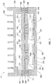
- FIG. 1 shows a cross-section view of solid-state drive (SSD) 100.
- SSD solid-state drive
- the SSD 100 is not an embodiment of the invention, but is provided as background information that is useful for understanding the invention.
- the cross-section views of FIGS. 1 to 3 are not drawn to scale to provide a clearer understanding of the present disclosure.
- SSD 100 includes a frame with upper frame portion 118 and lower frame portion 142, with printed circuit board (PCB) 102 mounted into or on lower frame portion 142.
- Upper frame portion 118 and lower frame portion 142 are sized to fit a particular form factor for SSD 100 such as a 2.5 inch form factor.
- Frame portions 118 and 142 can be comprised of a thermally conductive material to dissipate heat from SSD 100.
- a frame material can include, for example, an aluminum alloy such as 6061-T6 with a thermal conductivity of 167 W/mK.
- System on a chip (SOC) 110 is mounted on a bottom side of PCB 102 along with DDR 104, and flash memories 1 08 and 114. As shown in FIG. 1 , DDR 113 and flash memories 106 and 116 are mounted on a top side of PCB 102. Although one arrangement of heat generating components is shown in FIG. 1 , those of ordinary skill in the art will appreciate that the present disclosure is not limited to the specific quantities or a particular arrangement of components on PCB 102. For example, other examples can include more or less of the components shown in FIG. 1 mounted on a single side of PCB 102.
- SOC 110 is an integrated circuit (IC) which can serve as a controller for managing data in SSD 100.
- DDRs 113 and 104 are ICs which provide volatile memory for storing data.
- DDRs 113 and 104 can include, for example, double data rate synchronous dynamic random-access memory (DDR SDRAM) such as DDR SDRAM, DDR2 SDRAM, or DDR3 SDRAM.
- DDR SDRAM double data rate synchronous dynamic random-access memory
- flash memories 106, 108, 120 and 122 provide a nonvolatile memory (NVM) for storing data and can include, for example, NAND flash memory. While the example of FIG. 1 includes flash memory, other examples can include any type of solid-state memory.
- NVM nonvolatile memory
- solid- state memory may comprise one or more of various types of memory devices such as Chalcogenide RAM (C-RAM), Phase Change Memory (PC-RAM or PRAM), Programmable Metallization Cell RAM (PMC-RAM or PMCm), Ovonic Unified Memory (OUM), Resistance RAM (RRAM), NAND memory (e.g., single-level cell (SLC) memory, multi-level cell (MLC) memory, or any combination thereof), NOR memory, EEPROM, Ferroelectric Memory (FeRAM), Magnetoresistive RAM (MRAM), other discrete NVM chips, or any combination thereof.
- C-RAM Chalcogenide RAM
- PC-RAM or PRAM Phase Change Memory
- PMC-RAM or PMCm Programmable Metallization Cell RAM
- OFUM Ovonic Unified Memory
- RRAM Resistance RAM
- NAND memory e.g., single-level cell (SLC) memory, multi-level cell (MLC) memory, or any combination thereof
- NOR memory EEPROM
- Ferroelectric Memory FeRAM
- MRAM Magnetores
- SSD 100 also includes thermal interface material (TIM) layers 112, 114, 116, 117 and 119 which provide thermally conductive layers between portions of the frame on one side and components mounted on PCB 102 on another side.
- TIM layers 112, 114, 116, 117 and 119 can include any thermal interface material or combination of materials known in the art for conducting heat such as a phase change metal alloy (PCMA), graphene, or a silicone based material.
- PCMA phase change metal alloy
- TIM layers 112, 114, 116, 117 and 119 can have a thermal conductivity of 1 to 6 W/mK in a particular direction through the TIM layers.
- the TIM layers can include a flexible material or a thermal grease to improve thermal conductivity by filling air gaps due to surface imperfections on frame portions 118 and 142 and on components mounted on PCB 102.
- TIM layer 112 is separated from (i.e., not in direct contact with) TIM layer 117 along the inside surface of lower frame portion 142 by gap 115 which can include air.
- gap 115 can include air.
- One reason for separating TIM layers is to reduce heat transfer from a higher heat generating component to other components of SSD 100.
- TIM layer 112 is separated from TIM layer 117 to reduce heat transfer from SOC 110 to DDR 104 and flash memories 108 and 114 since these components may be susceptible to overheating.
- SOC 110 ordinarily generates significantly more heat than DDR 104 and flash memories 108 and 114.
- SOC 110 may generate 2 to 8 Watts compared to approximately 300 milliwatts generated by DDRs 104 and 113, and approximately 500 milliwatts generated by flash memories 106, 108, 120 and 122.
- TIM layers 112 and 117 are therefore separated to prevent heat transfer from SOC 1 10 to other components of SSD 100.
- TIM layers 114 and 117 are separated from each other along the inside surface of lower frame portion 142 by gap 105 to reduce heat which might otherwise conduct between DDR 104 and flash memories 108 and 122.
- TIM layers 116 and 119 are separated from each other by gap 107 along the inside surface of upper frame portion 118.
- FIG. 1 also includes graphene layers 123 (i.e., graphite sheets) between upper frame portion 118 and lower frame portion 142 which act as a heat spreader and thermally conductive layer between upper frame portion 118 and lower frame portion 142.
- graphene layers 123 ordinarily allow for better heat transfer between upper frame portion 118 and lower frame portion 142. Due to its high thermal conductivity (approximately 1500 Watts/meter-Kelvin in a parallel x-y plane and approximately 15 Watts/meter- Kelvin in a perpendicular z plane), graphene may also be used in TIM layers 112, 114, 116, 117 and 119.
- graphene layers 123 may be omitted so that frame portions 118 and 142 are in direct contact with each other. In yet other examples graphene layers 123 may be replaced with a different type of thermally conductive layer such as a thermal grease.
- FIG. 2 shows a cross-section view of a portion of SSD 200.
- the SSD 200 is not an embodiment of the invention, but is provided as background information that is useful for understanding the invention.
- SSD 200 includes frame 218 which is mounted on PCB 202.
- SOC 210 is also mounted on PCB 202 via solder balls 212.
- PCB 202 includes plane 204 which serves as a thermally conductive layer on one side of SOC 210.
- Plane 204 can include copper and may also serve as an electrical conductor for providing a ground or for transmitting a signal between components mounted on PCB 202 such as SOC 210 and memory components (not shown).
- plane 204 can be a dedicated thermal conduction plane to direct heat transfer from SOC 210 to frame 218 without connecting to other components on PCB 202.
- PCB 202 may include multiple planes. Certain planes, such as plane 204, may be predisposed for thermal conduction by being thicker than other planes and/or using a material (e.g., copper) with a heavier weight and/or a higher thermal conductivity than materials in other planes. In addition, such thermal conduction planes may be located closer to an outer surface of PCB 202 to better improve heat transfer.
- plane 204 may be predisposed for thermal conduction by being thicker than other planes and/or using a material (e.g., copper) with a heavier weight and/or a higher thermal conductivity than materials in other planes.
- thermal conduction planes may be located closer to an outer surface of PCB 202 to better improve heat transfer.
- SOC 210 is connected to plane 204 through balls 212 and vias 208 (e.g., microvias).
- Balls 212 can be part of a ball grid array (BGA) for mounting SOC 210 on PCB 202.
- BGA ball grid array
- Vias 206 provide a thermally conductive path from plane 204 to frame 218 through graphene layers 223.
- frame 21 8 is connected to PCB 202 so as to define a first thermally conductive path between the frame and SOC 210.
- the first thermally conductive path is illustrated with arrows 222 and 220, which represent heat being extracted from SOC 210 to frame 218 through balls 212, vias 208, plane 204, vias 206 and graphene layers 223.
- certain vias such as vias 206 and/or vias 208 may be predisposed for thermal conduction by being thicker than other vias and/or by using a material (e.g., copper) with a heavier weight and/or a higher thermal conductivity than materials in other vias.
- a material e.g., copper
- thermal conduction vias may be located to better improve heat transfer.
- TIM layer 214 is located between SOC 210 and graphene layer 21 6 so as to define a second thermally conductive path between frame 218 and SOC 210.
- TIM layer 214 is located between SOC 210 and graphene layer 21 6 so as to define a second thermally conductive path between frame 218 and SOC 210.
- the second thermally conductive path is illustrated with arrows 228 which represent heat being extracted from SOC 210 to frame 218 through TIM layer 214 and graphene layer 216. Since graphene layer 216 extends along a length of frame 218, graphene layer 21 6 spreads heat over the interior surface of frame 218 to increase heat transfer to frame 218.
- TIM layer 214 can include any thermal interface material or combination of materials known in the art for conducting heat such as a phase change metal alloy (PCMA), graphene, or a silicone based material.
- TIM layer 214 can include a flexible material or a thermal grease to improve thermal conductivity by filling air gaps due to surface imperfections on SOC 210.
- TIM layer 214 or graphene layer 216 may be omitted from the second thermally conductive path such that the thermally conductive layer between SOC 210 and frame 218 only includes graphene layer 21 6 or TIM layer 214.
- FIG. 3 shows a cross-section view of a portion of SSD 300 according to an embodiment of the invention.
- SSD 300 includes upper frame portion 318 and lower frame portion 342 which are mounted on PCB 302.
- SOC 310 and flash memory 309 are also mounted on a bottom side of PCB 302 via balls 312.
- PCB 302 includes plane 304 which serves as a thermally conductive layer on one side of flash memory 309 and SOC 310.
- Plane 304 can include copper and may also serve as an electrical conductor for providing a ground or for transmitting a signal between other components mounted on PCB 302.
- PCB 302 may include multiple planes.
- certain planes, such as plane 304 may be predisposed for thermal conduction as discussed above with reference to FIG. 2 .
- thermal conduction planes may be located closer to an outer surface of PCB 302 to better improve heat transfer.
- plane 304 includes break 321 such that plane 304 is not continuous across its total length. Breaks such as break 321 serve to direct heat transfer and may reduce heat transfer from high heat components such as SOC 310 to lower heat components such as flash memory 309. Other embodiments may also include multiple dedicated thermal conduction planes within PCB 302 to direct heat transfer and/or reduce heat transfer between components mounted on PCB 302.
- flash memory 309 and SOC 310 are connected to plane 304 through balls 312 and vias 308.
- upper frame 318 and lower frame 342 are connected to PCB 302 so as to define thermally conductive paths between the frame and SOC 310.
- thermally conductive paths there are two thermally conductive paths to the frame.
- the first thermally conductive path from flash memory 309 is illustrated with arrows 320 and 324 which represent heat being extracted from flash memory 309 to frame portions 318 and 342 through balls 312, vias 308, plane 304, vias 306, and a graphene layer 323.
- vias 306 and 308 may be predisposed for thermal conduction by being thicker than other vias and/or using a material (e.g., copper) with a heavier weight and/or a higher thermal conductivity than materials in other vias.
- thermal conduction vias may be located to better improve heat transfer.
- the second thermally conductive path from flash memory 309 is illustrated with arrows 330 which represent heat being extracted from flash memory 309 to lower frame portion 342 through TIM layer 313 and graphene layer 315.
- arrows 330 represent heat being extracted from flash memory 309 to lower frame portion 342 through TIM layer 313 and graphene layer 315.
- FIG. 3 shows gap 317 between TIM layers 313 and 314 and between graphene layers 315 and 316.
- Gap 317 may include air to reduce conduction of heat between flash memory 309 and SOC 310.
- graphene layers 315 and 316 extend in opposite directions from gap 317 which further directs heat from gap 317 as a result of the high thermal conductivity along the lengths of graphene layers 315 and 316.
- thermally conductive paths from SOC 310 there are two thermally conductive paths from SOC 310 to the frame.
- the first thermally conductive path from SOC 310 is illustrated with arrows 316 and 322 which represent heat being extracted from SOC 310 to frame portions 318 and 342 through balls 312, vias 308, plane 304, vias 306, and a graphene layer 323.
- vias 306 and 308 may be predisposed for thermal conduction by being thicker than other vias and/or using a material (e.g., copper) with a heavier weight and/or a higher thermal conductivity than materials in other vias.
- thermal conduction vias may be located to better improve heat transfer.
- the second thermally conductive path from SOC 310 is illustrated with arrows 328 which represent heat being extracted from SOC 310 to lower frame portion 342 through TIM layer 314 and graphene layer 316.
- arrows 328 represent heat being extracted from SOC 310 to lower frame portion 342 through TIM layer 314 and graphene layer 316.
- upper frame portion 318 includes exterior protrusions such as fins 334 and 336 which have different shapes to improve fluid flow over SSD 300 for convective cooling.
- the shapes and sizes of the exterior protrusions can vary based on different design considerations.
- exterior protrusions on the frame ordinarily improve heat transfer with exterior fluids (e.g., air, helium) by increasing a surface area of the frame and/or by adding material to the frame for heat sinking.
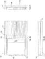
- FIGS. 4A and 4B provide a top view and a side view of an exterior of SSD 400 according to an embodiment.
- SSD 400 includes upper frame portion 420 (i.e., top cover) with exterior protrusions such as fins 434 and 436 which define channels between the exterior protrusions.
- the exterior protrusions ordinarily improve heat transfer from SSD 400 to an ambient fluid such as air or helium by increasing the exterior surface area of the frame.
- a fluid flows over SSD 400 to provide convective cooling.
- the extra surface area of the exterior protrusions increases heat dissipation from SSD 400 when fluid is not flowing over SSD 400.
- the exterior protrusions also add mass to the frame for heat sinking.
- exterior frame protrusions in FIGS. 4A and 4B are depicted as fins having a rectangular shape, other embodiments can include exterior protrusions having a different shape such as a cylindrical shape (i.e., pins) to increase the surface area and/or mass of the frame.
- a cylindrical shape i.e., pins
- Upper frame portion 420 and/or lower frame portion 418 can be etched to remove coatings from the frame that may otherwise hinder thermal conductivity.
- SSD 400 can be etched at specific locations where SSD 400 is to be mounted so as to provide thermally conductive paths from the exterior of SSD 400. Such etching can be performed with an etching laser or a chemical removal of surface coatings.
- SSD 400 includes raised potion 440 which provides an area for locating thermally conductive label 438.
- Labels may be provided as part of a standard for indicating characteristics of a data storage device on its exterior.
- Thermally conductive label 438 can be made of aluminum or another material having a relatively high (non-insulating) thermal conductivity to dissipate heat from SSD 400 in an area which might otherwise not dissipate much heat with a conventional label.
- Label 438 may also include a thermally conductive adhesive for affixing label 438 to SSD 400 while allowing for heat dissipation.
- Raised portion 440 also serves to house components in SSD 400 which would not otherwise fit under upper frame portion 420. By housing taller components under raised portion 440, exterior protrusions can be added to areas around raised portion 440 without increasing an overall height of SSD 400. In this regard, raised portion 440 may also be used to house stacked PCBs within SSD 400 to achieve a smaller footprint for SSD 400 while allowing room for exterior protrusions within an overall height specification for SSD 400.
- raised portion 440 includes ramp 442 on its right side so as to reduce the turbulence of fluid flowing raised portion 440.
- Ramp 442 includes exterior protrusions on its top surface and can be positioned to receive a flow from a particular direction such as from a fan (not shown) outside of SSD 400.
- fluid flows from the right side of SSD 400 toward the left side of SSD 400.
- Other embodiments may include other modifications to frame portions such as lower frame portion 418 or upper frame portion 420 to increase fluid flow over SSD 400 and thereby increase convective cooling of SSD 400.
- FIGS. 5A, 5B and 5C provide top and side views of an exterior SSD 500 according to an embodiment.
- SSD 500 includes exterior protrusions such as fins 534 and 536 which define channels on upper frame portion 520 between the fins.
- the fins of SSD 500 are longer in a direction of fluid flow over SSD 500. The longer fins of SSD 500 ordinarily reduce turbulence and increase the fluid flow over SSD 500 to increase heat dissipation from SSD 500.
- SSD 500 also includes a lower frame portion 518, a thermally conductive label 538, a raised portion 540, and a ramp 542. As shown in FIG. 5A , exterior protrusions such as fin 536 cut into ramp 542. As with SSD 400 of FIGS. 4A and 4B , the frame of SSD 500 may also be etched to remove coatings from the frame that may hinder thermal conductivity.
- FIGS. 6A, 6B and 6C provide top and side views of an exterior of SSD 600 according to an embodiment.
- SSD 600 includes exterior protrusions such as fins 634, 636, and 642 which define channels on upper frame portion 620 between the fins. Unlike SSD 500, the exterior protrusions of SSD 600 define channels in two directions. Although the fins of SSD 600 are longer in a direction of fluid flow over SSD 600, channels are provided along a width of the fins to increase a surface area of upper frame portion 620 and/or improve convective cooling from a fluid flow in a second direction.
- SSD 600 also includes lower frame portion 618, raised portion 640 and thermally conductive label 638.
Landscapes
- Engineering & Computer Science (AREA)
- Theoretical Computer Science (AREA)
- Chemical & Material Sciences (AREA)
- Physics & Mathematics (AREA)
- Nanotechnology (AREA)
- Microelectronics & Electronic Packaging (AREA)
- General Physics & Mathematics (AREA)
- General Engineering & Computer Science (AREA)
- Human Computer Interaction (AREA)
- Mathematical Physics (AREA)
- Crystallography & Structural Chemistry (AREA)
- Power Engineering (AREA)
- Cooling Or The Like Of Electrical Apparatus (AREA)
- Cooling Or The Like Of Semiconductors Or Solid State Devices (AREA)
- Materials Engineering (AREA)
Claims (14)
- Dispositif électronique (200, 300, 400, 500, 600) comprenant :une carte de circuit imprimé, PCB (202, 302), comprenant un plan de conduction thermique (204, 304) ;au moins un composant de génération de chaleur (210, 309, 310) monté sur une première surface de la PCB et connecté au plan de conduction thermique par l'intermédiaire de premiers trous d'interconnexion (208, 308) qui s'étendent dans la première surface de la PCB ;un cadre (218, 342) connecté à la PCB de manière à définir un premier trajet thermiquement conducteur entre au moins une partie du cadre et le au moins un composant de génération de chaleur, le premier trajet thermiquement conducteur comprenant les premiers trous d'interconnexion, le plan de conduction thermique, et des trous d'interconnexion (206, 306) qui s'étendent entre le plan de conduction thermique et le cadre ; etau moins une couche thermiquement conductrice (214, 313, 314) entre le cadre et le au moins un composant de génération de chaleur de manière à définir un second trajet thermiquement conducteur entre au moins une partie du cadre et le au moins un composant de génération de chaleur ;caractérisé en ce quele plan de conduction thermique comprend une rupture (321) telle qu'elle n'est pas continue sur une longueur totale du plan de conduction thermique, de manière à diriger un transfert de chaleur dans le plan de conduction thermique.
- Dispositif électronique selon la revendication 1, dans lequel la au moins une couche thermiquement conductrice comprend une couche de graphène.
- Dispositif électronique selon la revendication 1, dans lequel le au moins un composant de génération de chaleur comprend un premier composant de génération de chaleur et un second composant de génération de chaleur,
dans lequel la au moins une couche thermiquement conductrice comprend une première couche thermiquement conductrice entre le cadre et le premier composant de génération de chaleur et une seconde couche thermiquement conductrice entre le cadre et le second composant de génération de chaleur, et
dans lequel la première couche thermiquement conductrice ne vient pas en contact directement avec la seconde couche thermiquement conductrice de manière à réduire un transfert de chaleur entre les premier et second composants de génération de chaleur. - Dispositif électronique selon la revendication 1, dans lequel la PCB inclut une pluralité de plans et le plan de conduction thermique est prédisposé à une conduction thermique sur la base d'un emplacement du plan de conduction thermique, d'une taille du plan de conduction thermique, et/ou d'une composition de matériau du plan de conduction thermique.
- Dispositif électronique selon la revendication 1, dans lequel le cadre comprend une première partie (318) et une seconde partie (342) et le dispositif électronique comprend en outre au moins une couche de graphène (323) entre les première et seconde parties du cadre.
- Dispositif électronique selon la revendication 1, dans lequel la PCB est montée sur le cadre et le dispositif électronique comprend en outre au moins une couche de graphène (323) entre la PCB et le cadre.
- Dispositif électronique selon la revendication 1, dans lequel le cadre comprend des saillies extérieures (334, 336) pour augmenter une dissipation de chaleur à partir du dispositif électronique.
- Dispositif électronique selon la revendication 1, comprenant en outre une étiquette thermiquement conductrice (438, 538, 638) fixée au cadre, l'étiquette étant configurée pour indiquer des caractéristiques du dispositif électronique et dissiper de la chaleur provenant du dispositif électronique.
- Dispositif électronique selon la revendication 8, dans lequel l'étiquette thermiquement conductrice comprend de l'aluminium.
- Dispositif électronique selon la revendication 8, dans lequel l'étiquette thermiquement conductrice comprend un adhésif thermoconducteur.
- Dispositif électronique selon la revendication 1, dans lequel au moins une partie (418) de l'extérieur du cadre est gravée pour enlever un revêtement à partir du cadre.
- Dispositif électronique selon la revendication 1, dans lequel le cadre comprend une partie surélevée (440, 540, 640) logeant des composants du dispositif qui s'étendent au-delà de parties du cadre qui ne sont pas surélevées.
- Dispositif électronique selon la revendication 12, dans lequel la partie surélevée comprend une rampe (442, 542) pour réduire la turbulence d'un fluide s'écoulant au-dessus de la partie surélevée.
- Dispositif électronique selon la revendication 1, dans lequel le dispositif électronique est un lecteur à semiconducteur pour stocker des données.
Applications Claiming Priority (3)
| Application Number | Priority Date | Filing Date | Title |
|---|---|---|---|
| US201361811577P | 2013-04-12 | 2013-04-12 | |
| US13/904,992 US9123686B2 (en) | 2013-04-12 | 2013-05-29 | Thermal management for solid-state drive |
| PCT/US2014/033699 WO2014169152A1 (fr) | 2013-04-12 | 2014-04-10 | Gestion thermique pour dispositif de pilotage à semi-conducteurs |
Publications (3)
| Publication Number | Publication Date |
|---|---|
| EP2984652A1 EP2984652A1 (fr) | 2016-02-17 |
| EP2984652A4 EP2984652A4 (fr) | 2017-01-04 |
| EP2984652B1 true EP2984652B1 (fr) | 2021-06-16 |
Family
ID=51686223
Family Applications (1)
| Application Number | Title | Priority Date | Filing Date |
|---|---|---|---|
| EP14782613.5A Active EP2984652B1 (fr) | 2013-04-12 | 2014-04-10 | Gestion thermique pour dispositif de contrôle semi-conducteur |
Country Status (7)
| Country | Link |
|---|---|
| US (2) | US9123686B2 (fr) |
| EP (1) | EP2984652B1 (fr) |
| KR (2) | KR101888234B1 (fr) |
| CN (1) | CN105264612B (fr) |
| AU (3) | AU2014250916B2 (fr) |
| HK (1) | HK1216204A1 (fr) |
| WO (1) | WO2014169152A1 (fr) |
Families Citing this family (31)
| Publication number | Priority date | Publication date | Assignee | Title |
|---|---|---|---|---|
| KR102445662B1 (ko) | 2015-07-01 | 2022-09-22 | 삼성전자주식회사 | 스토리지 장치 |
| KR102361637B1 (ko) | 2015-08-25 | 2022-02-10 | 삼성전자주식회사 | 솔리드 스테이트 드라이브 장치 |
| US10085364B2 (en) | 2016-08-11 | 2018-09-25 | Seagate Technology Llc | SSD internal thermal transfer element |
| KR102546241B1 (ko) | 2016-10-05 | 2023-06-22 | 삼성전자주식회사 | 반도체 패키지 |
| KR102824610B1 (ko) | 2016-11-14 | 2025-06-25 | 삼성전자주식회사 | 반도체 모듈 |
| CN108304048B (zh) * | 2017-01-12 | 2021-04-13 | 上海宝存信息科技有限公司 | 服务器及其固态储存装置 |
| KR102777271B1 (ko) | 2017-02-28 | 2025-03-10 | 삼성전자주식회사 | 데이터 저장 장치, 그의 동작 방법 및 그를 포함하는 전자 시스템 |
| JP2018157005A (ja) * | 2017-03-16 | 2018-10-04 | 東芝メモリ株式会社 | 電子機器 |
| US10937464B2 (en) * | 2017-03-17 | 2021-03-02 | Intel Corporation | Solid state memory case with enhanced cooling |
| JP2019054216A (ja) * | 2017-09-19 | 2019-04-04 | 東芝メモリ株式会社 | 半導体装置 |
| KR102613515B1 (ko) | 2018-01-05 | 2023-12-13 | 삼성전자주식회사 | 솔리드 스테이트 드라이브 장치 및 이를 가지는 데이터 저장 시스템 |
| CN110060712A (zh) * | 2018-01-19 | 2019-07-26 | 创意电子股份有限公司 | 固态储存装置 |
| KR102615769B1 (ko) * | 2018-05-18 | 2023-12-20 | 삼성전자주식회사 | 메모리 장치 |
| US11901264B2 (en) * | 2018-10-31 | 2024-02-13 | Sk Hynix Nand Product Solutions Corp. | Choked flow cooling |
| US10798839B2 (en) | 2019-02-13 | 2020-10-06 | Cisco Technology, Inc. | Thermal management cage for a solid state drive |
| US11429163B2 (en) * | 2019-05-20 | 2022-08-30 | Western Digital Technologies, Inc. | Hot spot cooling for data storage system |
| US11013141B2 (en) * | 2019-05-31 | 2021-05-18 | Microsoft Technology Licensing, Llc | Decoupled conduction/convection dual heat sink for on-board memory microcontrollers |
| WO2021002387A1 (fr) * | 2019-07-04 | 2021-01-07 | パナソニックIpマネジメント株式会社 | Unité de dispositif de stockage |
| US11923264B2 (en) | 2019-09-20 | 2024-03-05 | Samsung Electronics Co., Ltd. | Semiconductor apparatus for discharging heat |
| US10980152B1 (en) * | 2019-11-11 | 2021-04-13 | Seagate Technology Llc | Thermal rectification with phase change materials |
| US11854932B2 (en) * | 2019-12-19 | 2023-12-26 | Intel Corporation | Package wrap-around heat spreader |
| CN111180426B (zh) * | 2019-12-31 | 2023-09-22 | 江苏长电科技股份有限公司 | 一种带石墨烯层散热的封装结构及其制造方法 |
| US11099618B1 (en) | 2020-01-27 | 2021-08-24 | Seagate Technology Llc | Compact portable data storage device |
| CN111723507B (zh) * | 2020-06-22 | 2021-05-04 | 西华大学 | 一种多层pcb结构稳态热分析方法 |
| CN116669282A (zh) * | 2020-08-31 | 2023-08-29 | 华为技术有限公司 | 一种散热组件及汽车 |
| JP2022147620A (ja) | 2021-03-23 | 2022-10-06 | キオクシア株式会社 | メモリシステム、及びラベル部品 |
| US11997782B2 (en) * | 2021-08-27 | 2024-05-28 | Micron Technology, Inc. | Thermally conductive label for circuit |
| US12158785B2 (en) * | 2022-02-10 | 2024-12-03 | Micron Technology, Inc. | Thermal islanding heatsink |
| US11985782B2 (en) * | 2022-04-08 | 2024-05-14 | Western Digital Technologies, Inc. | Enclosure fitting for electronic device |
| US20240244779A1 (en) * | 2023-01-18 | 2024-07-18 | Micron Technology, Inc. | Solid state drive enclosure |
| KR20240157917A (ko) * | 2023-04-26 | 2024-11-04 | 에스케이하이닉스 주식회사 | 외장 데이터 저장 장치 |
Citations (2)
| Publication number | Priority date | Publication date | Assignee | Title |
|---|---|---|---|---|
| US6246583B1 (en) * | 1999-03-04 | 2001-06-12 | International Business Machines Corporation | Method and apparatus for removing heat from a semiconductor device |
| US20020084524A1 (en) * | 2001-01-04 | 2002-07-04 | Samsung Electronics Co., Ltd. | Ball grid array package comprising a heat sink |
Family Cites Families (87)
| Publication number | Priority date | Publication date | Assignee | Title |
|---|---|---|---|---|
| US4471837A (en) * | 1981-12-28 | 1984-09-18 | Aavid Engineering, Inc. | Graphite heat-sink mountings |
| US5467251A (en) * | 1993-10-08 | 1995-11-14 | Northern Telecom Limited | Printed circuit boards and heat sink structures |
| FR2766967A1 (fr) * | 1997-07-31 | 1999-02-05 | Scps | Dispositif de dissipation thermique et/ou protection electromagnetique pour cartes et composants electroniques |
| US7301776B1 (en) | 2004-11-16 | 2007-11-27 | Super Talent Electronics, Inc. | Light-weight flash hard drive with plastic frame |
| US6519154B1 (en) * | 2001-08-17 | 2003-02-11 | Intel Corporation | Thermal bus design to cool a microelectronic die |
| US7006354B2 (en) * | 2001-10-26 | 2006-02-28 | Fujikura Ltd. | Heat radiating structure for electronic device |
| US7023699B2 (en) * | 2002-06-10 | 2006-04-04 | Visteon Global Technologies, Inc. | Liquid cooled metal thermal stack for high-power dies |
| EP1562230B1 (fr) | 2002-11-12 | 2017-07-05 | Fujitsu Limited | Structure d'emballage |
| US6856556B1 (en) | 2003-04-03 | 2005-02-15 | Siliconsystems, Inc. | Storage subsystem with embedded circuit for protecting against anomalies in power signal from host |
| US20050196904A1 (en) * | 2004-03-05 | 2005-09-08 | Anandaroop Bhattacharya | Aerodynamic memory module cover |
| US7286359B2 (en) | 2004-05-11 | 2007-10-23 | The U.S. Government As Represented By The National Security Agency | Use of thermally conductive vias to extract heat from microelectronic chips and method of manufacturing |
| WO2006024009A2 (fr) | 2004-08-24 | 2006-03-02 | C-Core Technologies, Inc. | Cartes imprimees a bord metallise |
| US7502256B2 (en) | 2004-11-30 | 2009-03-10 | Siliconsystems, Inc. | Systems and methods for reducing unauthorized data recovery from solid-state storage devices |
| US7653778B2 (en) | 2006-05-08 | 2010-01-26 | Siliconsystems, Inc. | Systems and methods for measuring the useful life of solid-state storage devices |
| JP2007332293A (ja) | 2006-06-16 | 2007-12-27 | Panac Co Ltd | 粘着ラベル |
| US7765373B1 (en) | 2006-06-27 | 2010-07-27 | Siliconsystems, Inc. | System for controlling use of a solid-state storage subsystem |
| US8108692B1 (en) | 2006-06-27 | 2012-01-31 | Siliconsystems, Inc. | Solid-state storage subsystem security solution |
| US7447807B1 (en) | 2006-06-30 | 2008-11-04 | Siliconsystems, Inc. | Systems and methods for storing data in segments of a storage subsystem |
| US7509441B1 (en) | 2006-06-30 | 2009-03-24 | Siliconsystems, Inc. | Systems and methods for segmenting and protecting a storage subsystem |
| US8161227B1 (en) | 2006-10-30 | 2012-04-17 | Siliconsystems, Inc. | Storage subsystem capable of programming field-programmable devices of a target computer system |
| KR100843214B1 (ko) | 2006-12-05 | 2008-07-02 | 삼성전자주식회사 | 메모리 칩과 프로세서 칩이 관통전극을 통해 연결된 플래너멀티 반도체 칩 패키지 및 그 제조방법 |
| US8549236B2 (en) | 2006-12-15 | 2013-10-01 | Siliconsystems, Inc. | Storage subsystem with multiple non-volatile memory arrays to protect against data losses |
| US7596643B2 (en) | 2007-02-07 | 2009-09-29 | Siliconsystems, Inc. | Storage subsystem with configurable buffer |
| US7685337B2 (en) | 2007-05-24 | 2010-03-23 | Siliconsystems, Inc. | Solid state storage subsystem for embedded applications |
| US7685338B2 (en) | 2007-05-24 | 2010-03-23 | Siliconsystems, Inc. | Solid state storage subsystem for embedded applications |
| US7790511B2 (en) | 2007-06-11 | 2010-09-07 | International Business Machines Corporation | Method for direct heat sink attachment |
| US7685374B2 (en) | 2007-07-26 | 2010-03-23 | Siliconsystems, Inc. | Multi-interface and multi-bus structured solid-state storage subsystem |
| US8095851B2 (en) | 2007-09-06 | 2012-01-10 | Siliconsystems, Inc. | Storage subsystem capable of adjusting ECC settings based on monitored conditions |
| US8078918B2 (en) | 2008-02-07 | 2011-12-13 | Siliconsystems, Inc. | Solid state storage subsystem that maintains and provides access to data reflective of a failure risk |
| US7962792B2 (en) | 2008-02-11 | 2011-06-14 | Siliconsystems, Inc. | Interface for enabling a host computer to retrieve device monitor data from a solid state storage subsystem |
| US7733712B1 (en) | 2008-05-20 | 2010-06-08 | Siliconsystems, Inc. | Storage subsystem with embedded circuit for protecting against anomalies in power signal from host |
| US20100128432A1 (en) | 2008-06-16 | 2010-05-27 | Miller Matthew P | System and method for virtual computing environment management, network interface manipulation and information indication |
| US8583835B1 (en) | 2008-08-06 | 2013-11-12 | Siliconsystems, Inc. | Command portal for executing non-standard storage subsystem commands |
| US8375151B1 (en) | 2009-02-12 | 2013-02-12 | Siliconsystems, Inc. | Command portal for securely communicating and executing non-standard storage subsystem commands |
| US20100097767A1 (en) | 2008-10-18 | 2010-04-22 | John David Jude | Machine for passively removing heat generated by an electronic circuit board |
| US8154116B2 (en) | 2008-11-03 | 2012-04-10 | HeadwayTechnologies, Inc. | Layered chip package with heat sink |
| US20100128439A1 (en) * | 2008-11-24 | 2010-05-27 | General Electric Company | Thermal management system with graphene-based thermal interface material |
| US9176859B2 (en) | 2009-01-07 | 2015-11-03 | Siliconsystems, Inc. | Systems and methods for improving the performance of non-volatile memory operations |
| US8090899B1 (en) | 2009-03-04 | 2012-01-03 | Western Digital Technologies, Inc. | Solid state drive power safe wear-leveling |
| US10079048B2 (en) | 2009-03-24 | 2018-09-18 | Western Digital Technologies, Inc. | Adjusting access of non-volatile semiconductor memory based on access time |
| CN105140136B (zh) | 2009-03-30 | 2018-02-13 | 高通股份有限公司 | 使用顶部后钝化技术和底部结构技术的集成电路芯片 |
| US8879263B2 (en) | 2009-08-17 | 2014-11-04 | Seagate Technology Llc | Conducting heat away from a printed circuit board assembly in an enclosure |
| US9078357B2 (en) | 2009-08-17 | 2015-07-07 | Seagate Technology Llc | Internal cover thermal conduction |
| US8254172B1 (en) | 2009-09-30 | 2012-08-28 | Western Digital Technologies, Inc. | Wear leveling non-volatile semiconductor memory based on erase times and program times |
| US8243525B1 (en) | 2009-09-30 | 2012-08-14 | Western Digital Technologies, Inc. | Refreshing non-volatile semiconductor memory by reading without rewriting |
| US9753847B2 (en) | 2009-10-27 | 2017-09-05 | Western Digital Technologies, Inc. | Non-volatile semiconductor memory segregating sequential, random, and system data to reduce garbage collection for page based mapping |
| US8261012B2 (en) | 2009-10-30 | 2012-09-04 | Western Digital Technologies, Inc. | Non-volatile semiconductor memory comprising power fail circuitry for flushing write data in response to a power fail signal |
| US8135903B1 (en) | 2009-10-30 | 2012-03-13 | Western Digital Technologies, Inc. | Non-volatile semiconductor memory compressing data to improve performance |
| US8397107B1 (en) | 2009-12-11 | 2013-03-12 | Western Digital Technologies, Inc. | Data storage device employing data path protection using both LBA and PBA |
| US8443167B1 (en) | 2009-12-16 | 2013-05-14 | Western Digital Technologies, Inc. | Data storage device employing a run-length mapping table and a single address mapping table |
| US8316176B1 (en) | 2010-02-17 | 2012-11-20 | Western Digital Technologies, Inc. | Non-volatile semiconductor memory segregating sequential data during garbage collection to reduce write amplification |
| US8407449B1 (en) | 2010-02-26 | 2013-03-26 | Western Digital Technologies, Inc. | Non-volatile semiconductor memory storing an inverse map for rebuilding a translation table |
| CN201629939U (zh) * | 2010-03-04 | 2010-11-10 | 成都市华为赛门铁克科技有限公司 | 固态硬盘 |
| US9026716B2 (en) | 2010-05-12 | 2015-05-05 | Western Digital Technologies, Inc. | System and method for managing garbage collection in solid-state memory |
| US8341339B1 (en) | 2010-06-14 | 2012-12-25 | Western Digital Technologies, Inc. | Hybrid drive garbage collecting a non-volatile semiconductor memory by migrating valid data to a disk |
| US8612669B1 (en) | 2010-06-28 | 2013-12-17 | Western Digital Technologies, Inc. | System and method for performing data retention in solid-state memory using copy commands and validity and usage data |
| US8447920B1 (en) | 2010-06-29 | 2013-05-21 | Western Digital Technologies, Inc. | System and method for managing data access in non-volatile memory |
| US8521972B1 (en) | 2010-06-30 | 2013-08-27 | Western Digital Technologies, Inc. | System and method for optimizing garbage collection in data storage |
| TWM399588U (en) | 2010-08-05 | 2011-03-01 | Unimicron Technology Corp | wiring board |
| US8639872B1 (en) | 2010-08-13 | 2014-01-28 | Western Digital Technologies, Inc. | Hybrid drive comprising write cache spanning non-volatile semiconductor memory and disk |
| US8638602B1 (en) | 2010-09-10 | 2014-01-28 | Western Digital Technologies, Inc. | Background selection of voltage reference values for performing memory read operations |
| US8612804B1 (en) | 2010-09-30 | 2013-12-17 | Western Digital Technologies, Inc. | System and method for improving wear-leveling performance in solid-state memory |
| US8601313B1 (en) | 2010-12-13 | 2013-12-03 | Western Digital Technologies, Inc. | System and method for a data reliability scheme in a solid state memory |
| US8615681B2 (en) | 2010-12-14 | 2013-12-24 | Western Digital Technologies, Inc. | System and method for maintaining a data redundancy scheme in a solid state memory in the event of a power loss |
| US8601311B2 (en) | 2010-12-14 | 2013-12-03 | Western Digital Technologies, Inc. | System and method for using over-provisioned data capacity to maintain a data redundancy scheme in a solid state memory |
| US8458435B1 (en) | 2010-12-20 | 2013-06-04 | Western Digital Technologies, Inc. | Sequential write thread detection |
| US8392635B2 (en) | 2010-12-22 | 2013-03-05 | Western Digital Technologies, Inc. | Selectively enabling a host transfer interrupt |
| US8683113B2 (en) | 2011-02-04 | 2014-03-25 | Western Digital Technologies, Inc. | Concurrently searching multiple devices of a non-volatile semiconductor memory |
| US8700950B1 (en) | 2011-02-11 | 2014-04-15 | Western Digital Technologies, Inc. | System and method for data error recovery in a solid state subsystem |
| US8537553B2 (en) * | 2011-02-14 | 2013-09-17 | Futurewei Technologies, Inc. | Devices having anisotropic conductivity heatsinks, and methods of making thereof |
| US8700951B1 (en) | 2011-03-09 | 2014-04-15 | Western Digital Technologies, Inc. | System and method for improving a data redundancy scheme in a solid state subsystem with additional metadata |
| US8769232B2 (en) | 2011-04-06 | 2014-07-01 | Western Digital Technologies, Inc. | Non-volatile semiconductor memory module enabling out of order host command chunk media access |
| US8862804B2 (en) | 2011-04-29 | 2014-10-14 | Western Digital Technologies, Inc. | System and method for improved parity determination within a data redundancy scheme in a solid state memory |
| US9021178B2 (en) | 2011-05-02 | 2015-04-28 | Western Digital Technologies, Inc. | High performance path for command processing |
| US8503237B1 (en) | 2011-05-18 | 2013-08-06 | Western Digital Technologies, Inc. | System and method for data recovery in a solid state storage device |
| US8719531B2 (en) | 2011-06-14 | 2014-05-06 | Western Digital Technologies, Inc. | System and method for performing data retention that incorporates environmental conditions |
| US8423722B1 (en) | 2011-08-26 | 2013-04-16 | Western Digital Technologies, Inc. | System and method for high performance command processing in solid state drives |
| US8700834B2 (en) | 2011-09-06 | 2014-04-15 | Western Digital Technologies, Inc. | Systems and methods for an enhanced controller architecture in data storage systems |
| US8707104B1 (en) | 2011-09-06 | 2014-04-22 | Western Digital Technologies, Inc. | Systems and methods for error injection in data storage systems |
| US8698258B2 (en) * | 2011-09-30 | 2014-04-15 | General Electric Company | 3D integrated electronic device structure including increased thermal dissipation capabilities |
| US8977803B2 (en) | 2011-11-21 | 2015-03-10 | Western Digital Technologies, Inc. | Disk drive data caching using a multi-tiered memory |
| US9003224B2 (en) | 2012-04-25 | 2015-04-07 | Western Digital Technologies, Inc. | Managing unreliable memory in data storage systems |
| CN102867793A (zh) * | 2012-08-14 | 2013-01-09 | 日月光半导体制造股份有限公司 | 热界面材料及半导体封装结构 |
| US8966343B2 (en) | 2012-08-21 | 2015-02-24 | Western Digital Technologies, Inc. | Solid-state drive retention monitor using reference blocks |
| US8972826B2 (en) | 2012-10-24 | 2015-03-03 | Western Digital Technologies, Inc. | Adaptive error correction codes for data storage systems |
| US9177638B2 (en) | 2012-11-13 | 2015-11-03 | Western Digital Technologies, Inc. | Methods and devices for avoiding lower page corruption in data storage devices |
| US8954694B2 (en) | 2012-11-15 | 2015-02-10 | Western Digital Technologies, Inc. | Methods, data storage devices and systems for fragmented firmware table rebuild in a solid state drive |
-
2013
- 2013-05-29 US US13/904,992 patent/US9123686B2/en active Active
-
2014
- 2014-04-10 WO PCT/US2014/033699 patent/WO2014169152A1/fr not_active Ceased
- 2014-04-10 KR KR1020157032235A patent/KR101888234B1/ko active Active
- 2014-04-10 CN CN201480020844.0A patent/CN105264612B/zh active Active
- 2014-04-10 HK HK16104179.7A patent/HK1216204A1/zh unknown
- 2014-04-10 AU AU2014250916A patent/AU2014250916B2/en active Active
- 2014-04-10 EP EP14782613.5A patent/EP2984652B1/fr active Active
- 2014-04-10 KR KR1020187022523A patent/KR20180091118A/ko not_active Ceased
-
2015
- 2015-07-27 US US14/810,391 patent/US9880594B2/en active Active
-
2018
- 2018-11-09 AU AU2018260954A patent/AU2018260954B2/en active Active
-
2019
- 2019-03-29 AU AU2019202222A patent/AU2019202222B2/en active Active
Patent Citations (2)
| Publication number | Priority date | Publication date | Assignee | Title |
|---|---|---|---|---|
| US6246583B1 (en) * | 1999-03-04 | 2001-06-12 | International Business Machines Corporation | Method and apparatus for removing heat from a semiconductor device |
| US20020084524A1 (en) * | 2001-01-04 | 2002-07-04 | Samsung Electronics Co., Ltd. | Ball grid array package comprising a heat sink |
Also Published As
| Publication number | Publication date |
|---|---|
| AU2019202222B2 (en) | 2020-06-25 |
| KR20180091118A (ko) | 2018-08-14 |
| US20150331460A1 (en) | 2015-11-19 |
| AU2014250916B2 (en) | 2018-08-09 |
| AU2014250916A1 (en) | 2015-10-29 |
| EP2984652A4 (fr) | 2017-01-04 |
| AU2018260954B2 (en) | 2019-05-16 |
| HK1216204A1 (zh) | 2016-10-21 |
| KR101888234B1 (ko) | 2018-08-13 |
| US9880594B2 (en) | 2018-01-30 |
| US20140306335A1 (en) | 2014-10-16 |
| KR20150142027A (ko) | 2015-12-21 |
| CN105264612A (zh) | 2016-01-20 |
| AU2019202222A1 (en) | 2019-04-18 |
| WO2014169152A1 (fr) | 2014-10-16 |
| AU2018260954A1 (en) | 2018-11-29 |
| US9123686B2 (en) | 2015-09-01 |
| EP2984652A1 (fr) | 2016-02-17 |
| CN105264612B (zh) | 2017-12-22 |
Similar Documents
| Publication | Publication Date | Title |
|---|---|---|
| EP2984652B1 (fr) | Gestion thermique pour dispositif de contrôle semi-conducteur | |
| US10551885B2 (en) | Solid state drive apparatus | |
| US11800686B2 (en) | Solid state drive apparatus and data storage apparatus including the same | |
| KR102767456B1 (ko) | 솔리드 스테이트 드라이브 장치 및 이를 포함하는 컴퓨터 서버 시스템 | |
| US9894805B2 (en) | Heat sink and memory module having the same | |
| KR102613515B1 (ko) | 솔리드 스테이트 드라이브 장치 및 이를 가지는 데이터 저장 시스템 | |
| JP6889814B1 (ja) | 複数の半導体デバイスモジュール内の熱を消散するための装置及び方法 | |
| CN105874890A (zh) | 基板组装件的散热 | |
| CN110473846B (zh) | 与半导体装置一起使用的散热器 | |
| KR20210001171A (ko) | 메모리 장치 | |
| US20160270266A1 (en) | Semiconductor memory device having a heat insulating mechanism | |
| JP2016071269A (ja) | 電子機器、及びシステム | |
| JP3100714U (ja) | 熱放散板モジュール | |
| CN102123575B (zh) | 散热模块及具有该散热模块的可携式电子装置 |
Legal Events
| Date | Code | Title | Description |
|---|---|---|---|
| PUAI | Public reference made under article 153(3) epc to a published international application that has entered the european phase |
Free format text: ORIGINAL CODE: 0009012 |
|
| 17P | Request for examination filed |
Effective date: 20151104 |
|
| AK | Designated contracting states |
Kind code of ref document: A1 Designated state(s): AL AT BE BG CH CY CZ DE DK EE ES FI FR GB GR HR HU IE IS IT LI LT LU LV MC MK MT NL NO PL PT RO RS SE SI SK SM TR |
|
| AX | Request for extension of the european patent |
Extension state: BA ME |
|
| RIN1 | Information on inventor provided before grant (corrected) |
Inventor name: CAMPBELL, TEGAN Inventor name: MATAYA, RICHARD A. |
|
| DAX | Request for extension of the european patent (deleted) | ||
| A4 | Supplementary search report drawn up and despatched |
Effective date: 20161207 |
|
| RIC1 | Information provided on ipc code assigned before grant |
Ipc: G11C 16/02 20060101AFI20161201BHEP Ipc: H01L 23/367 20060101ALI20161201BHEP Ipc: G11C 7/04 20060101ALI20161201BHEP |
|
| STAA | Information on the status of an ep patent application or granted ep patent |
Free format text: STATUS: REQUEST FOR EXAMINATION WAS MADE |
|
| STAA | Information on the status of an ep patent application or granted ep patent |
Free format text: STATUS: EXAMINATION IS IN PROGRESS |
|
| 17Q | First examination report despatched |
Effective date: 20191129 |
|
| GRAP | Despatch of communication of intention to grant a patent |
Free format text: ORIGINAL CODE: EPIDOSNIGR1 |
|
| STAA | Information on the status of an ep patent application or granted ep patent |
Free format text: STATUS: GRANT OF PATENT IS INTENDED |
|
| INTG | Intention to grant announced |
Effective date: 20210305 |
|
| GRAS | Grant fee paid |
Free format text: ORIGINAL CODE: EPIDOSNIGR3 |
|
| GRAA | (expected) grant |
Free format text: ORIGINAL CODE: 0009210 |
|
| STAA | Information on the status of an ep patent application or granted ep patent |
Free format text: STATUS: THE PATENT HAS BEEN GRANTED |
|
| RIN1 | Information on inventor provided before grant (corrected) |
Inventor name: CAMPBELL, TEGAN Inventor name: MATAYA, RICHARD A. |
|
| RAP3 | Party data changed (applicant data changed or rights of an application transferred) |
Owner name: WESTERN DIGITAL TECHNOLOGIES, INC. |
|
| AK | Designated contracting states |
Kind code of ref document: B1 Designated state(s): AL AT BE BG CH CY CZ DE DK EE ES FI FR GB GR HR HU IE IS IT LI LT LU LV MC MK MT NL NO PL PT RO RS SE SI SK SM TR |
|
| REG | Reference to a national code |
Ref country code: GB Ref legal event code: FG4D |
|
| REG | Reference to a national code |
Ref country code: CH Ref legal event code: EP |
|
| REG | Reference to a national code |
Ref country code: DE Ref legal event code: R096 Ref document number: 602014078159 Country of ref document: DE |
|
| REG | Reference to a national code |
Ref country code: AT Ref legal event code: REF Ref document number: 1402992 Country of ref document: AT Kind code of ref document: T Effective date: 20210715 |
|
| REG | Reference to a national code |
Ref country code: IE Ref legal event code: FG4D |
|
| REG | Reference to a national code |
Ref country code: NL Ref legal event code: FP |
|
| REG | Reference to a national code |
Ref country code: LT Ref legal event code: MG9D |
|
| PG25 | Lapsed in a contracting state [announced via postgrant information from national office to epo] |
Ref country code: LT Free format text: LAPSE BECAUSE OF FAILURE TO SUBMIT A TRANSLATION OF THE DESCRIPTION OR TO PAY THE FEE WITHIN THE PRESCRIBED TIME-LIMIT Effective date: 20210616 Ref country code: FI Free format text: LAPSE BECAUSE OF FAILURE TO SUBMIT A TRANSLATION OF THE DESCRIPTION OR TO PAY THE FEE WITHIN THE PRESCRIBED TIME-LIMIT Effective date: 20210616 Ref country code: BG Free format text: LAPSE BECAUSE OF FAILURE TO SUBMIT A TRANSLATION OF THE DESCRIPTION OR TO PAY THE FEE WITHIN THE PRESCRIBED TIME-LIMIT Effective date: 20210916 Ref country code: HR Free format text: LAPSE BECAUSE OF FAILURE TO SUBMIT A TRANSLATION OF THE DESCRIPTION OR TO PAY THE FEE WITHIN THE PRESCRIBED TIME-LIMIT Effective date: 20210616 |
|
| REG | Reference to a national code |
Ref country code: AT Ref legal event code: MK05 Ref document number: 1402992 Country of ref document: AT Kind code of ref document: T Effective date: 20210616 |
|
| PG25 | Lapsed in a contracting state [announced via postgrant information from national office to epo] |
Ref country code: GR Free format text: LAPSE BECAUSE OF FAILURE TO SUBMIT A TRANSLATION OF THE DESCRIPTION OR TO PAY THE FEE WITHIN THE PRESCRIBED TIME-LIMIT Effective date: 20210917 Ref country code: LV Free format text: LAPSE BECAUSE OF FAILURE TO SUBMIT A TRANSLATION OF THE DESCRIPTION OR TO PAY THE FEE WITHIN THE PRESCRIBED TIME-LIMIT Effective date: 20210616 Ref country code: NO Free format text: LAPSE BECAUSE OF FAILURE TO SUBMIT A TRANSLATION OF THE DESCRIPTION OR TO PAY THE FEE WITHIN THE PRESCRIBED TIME-LIMIT Effective date: 20210916 Ref country code: SE Free format text: LAPSE BECAUSE OF FAILURE TO SUBMIT A TRANSLATION OF THE DESCRIPTION OR TO PAY THE FEE WITHIN THE PRESCRIBED TIME-LIMIT Effective date: 20210616 Ref country code: RS Free format text: LAPSE BECAUSE OF FAILURE TO SUBMIT A TRANSLATION OF THE DESCRIPTION OR TO PAY THE FEE WITHIN THE PRESCRIBED TIME-LIMIT Effective date: 20210616 |
|
| PG25 | Lapsed in a contracting state [announced via postgrant information from national office to epo] |
Ref country code: PT Free format text: LAPSE BECAUSE OF FAILURE TO SUBMIT A TRANSLATION OF THE DESCRIPTION OR TO PAY THE FEE WITHIN THE PRESCRIBED TIME-LIMIT Effective date: 20211018 Ref country code: RO Free format text: LAPSE BECAUSE OF FAILURE TO SUBMIT A TRANSLATION OF THE DESCRIPTION OR TO PAY THE FEE WITHIN THE PRESCRIBED TIME-LIMIT Effective date: 20210616 Ref country code: ES Free format text: LAPSE BECAUSE OF FAILURE TO SUBMIT A TRANSLATION OF THE DESCRIPTION OR TO PAY THE FEE WITHIN THE PRESCRIBED TIME-LIMIT Effective date: 20210616 Ref country code: AT Free format text: LAPSE BECAUSE OF FAILURE TO SUBMIT A TRANSLATION OF THE DESCRIPTION OR TO PAY THE FEE WITHIN THE PRESCRIBED TIME-LIMIT Effective date: 20210616 Ref country code: CZ Free format text: LAPSE BECAUSE OF FAILURE TO SUBMIT A TRANSLATION OF THE DESCRIPTION OR TO PAY THE FEE WITHIN THE PRESCRIBED TIME-LIMIT Effective date: 20210616 Ref country code: EE Free format text: LAPSE BECAUSE OF FAILURE TO SUBMIT A TRANSLATION OF THE DESCRIPTION OR TO PAY THE FEE WITHIN THE PRESCRIBED TIME-LIMIT Effective date: 20210616 Ref country code: SK Free format text: LAPSE BECAUSE OF FAILURE TO SUBMIT A TRANSLATION OF THE DESCRIPTION OR TO PAY THE FEE WITHIN THE PRESCRIBED TIME-LIMIT Effective date: 20210616 Ref country code: SM Free format text: LAPSE BECAUSE OF FAILURE TO SUBMIT A TRANSLATION OF THE DESCRIPTION OR TO PAY THE FEE WITHIN THE PRESCRIBED TIME-LIMIT Effective date: 20210616 |
|
| PG25 | Lapsed in a contracting state [announced via postgrant information from national office to epo] |
Ref country code: PL Free format text: LAPSE BECAUSE OF FAILURE TO SUBMIT A TRANSLATION OF THE DESCRIPTION OR TO PAY THE FEE WITHIN THE PRESCRIBED TIME-LIMIT Effective date: 20210616 |
|
| REG | Reference to a national code |
Ref country code: DE Ref legal event code: R097 Ref document number: 602014078159 Country of ref document: DE |
|
| PLBE | No opposition filed within time limit |
Free format text: ORIGINAL CODE: 0009261 |
|
| STAA | Information on the status of an ep patent application or granted ep patent |
Free format text: STATUS: NO OPPOSITION FILED WITHIN TIME LIMIT |
|
| PG25 | Lapsed in a contracting state [announced via postgrant information from national office to epo] |
Ref country code: DK Free format text: LAPSE BECAUSE OF FAILURE TO SUBMIT A TRANSLATION OF THE DESCRIPTION OR TO PAY THE FEE WITHIN THE PRESCRIBED TIME-LIMIT Effective date: 20210616 |
|
| 26N | No opposition filed |
Effective date: 20220317 |
|
| PG25 | Lapsed in a contracting state [announced via postgrant information from national office to epo] |
Ref country code: AL Free format text: LAPSE BECAUSE OF FAILURE TO SUBMIT A TRANSLATION OF THE DESCRIPTION OR TO PAY THE FEE WITHIN THE PRESCRIBED TIME-LIMIT Effective date: 20210616 |
|
| PG25 | Lapsed in a contracting state [announced via postgrant information from national office to epo] |
Ref country code: IT Free format text: LAPSE BECAUSE OF FAILURE TO SUBMIT A TRANSLATION OF THE DESCRIPTION OR TO PAY THE FEE WITHIN THE PRESCRIBED TIME-LIMIT Effective date: 20210616 |
|
| REG | Reference to a national code |
Ref country code: CH Ref legal event code: PL |
|
| REG | Reference to a national code |
Ref country code: BE Ref legal event code: MM Effective date: 20220430 |
|
| PG25 | Lapsed in a contracting state [announced via postgrant information from national office to epo] |
Ref country code: MC Free format text: LAPSE BECAUSE OF FAILURE TO SUBMIT A TRANSLATION OF THE DESCRIPTION OR TO PAY THE FEE WITHIN THE PRESCRIBED TIME-LIMIT Effective date: 20210616 Ref country code: LU Free format text: LAPSE BECAUSE OF NON-PAYMENT OF DUE FEES Effective date: 20220410 Ref country code: LI Free format text: LAPSE BECAUSE OF NON-PAYMENT OF DUE FEES Effective date: 20220430 Ref country code: FR Free format text: LAPSE BECAUSE OF NON-PAYMENT OF DUE FEES Effective date: 20220430 Ref country code: CH Free format text: LAPSE BECAUSE OF NON-PAYMENT OF DUE FEES Effective date: 20220430 |
|
| PG25 | Lapsed in a contracting state [announced via postgrant information from national office to epo] |
Ref country code: BE Free format text: LAPSE BECAUSE OF NON-PAYMENT OF DUE FEES Effective date: 20220430 |
|
| PG25 | Lapsed in a contracting state [announced via postgrant information from national office to epo] |
Ref country code: IE Free format text: LAPSE BECAUSE OF NON-PAYMENT OF DUE FEES Effective date: 20220410 |
|
| P01 | Opt-out of the competence of the unified patent court (upc) registered |
Effective date: 20230606 |
|
| PG25 | Lapsed in a contracting state [announced via postgrant information from national office to epo] |
Ref country code: HU Free format text: LAPSE BECAUSE OF FAILURE TO SUBMIT A TRANSLATION OF THE DESCRIPTION OR TO PAY THE FEE WITHIN THE PRESCRIBED TIME-LIMIT; INVALID AB INITIO Effective date: 20140410 |
|
| PG25 | Lapsed in a contracting state [announced via postgrant information from national office to epo] |
Ref country code: MK Free format text: LAPSE BECAUSE OF FAILURE TO SUBMIT A TRANSLATION OF THE DESCRIPTION OR TO PAY THE FEE WITHIN THE PRESCRIBED TIME-LIMIT Effective date: 20210616 Ref country code: CY Free format text: LAPSE BECAUSE OF FAILURE TO SUBMIT A TRANSLATION OF THE DESCRIPTION OR TO PAY THE FEE WITHIN THE PRESCRIBED TIME-LIMIT Effective date: 20210616 |
|
| REG | Reference to a national code |
Ref country code: DE Ref legal event code: R081 Ref document number: 602014078159 Country of ref document: DE Owner name: WESTERN DIGITAL TECHNOLOGIES, INC. (N.D.GES.D., US Free format text: FORMER OWNER: WESTERN DIGITAL TECHNOLOGIES, INC., SAN JOSE, CALIF., US Ref country code: DE Ref legal event code: R081 Ref document number: 602014078159 Country of ref document: DE Owner name: SANDISK TECHNOLOGIES, INC. (N.D.GES.D. STAATES, US Free format text: FORMER OWNER: WESTERN DIGITAL TECHNOLOGIES, INC., SAN JOSE, CALIF., US Ref country code: DE Ref legal event code: R081 Ref document number: 602014078159 Country of ref document: DE Owner name: SANDISK TECHNOLOGIES, INC. (N.D.GES. D. STAATE, US Free format text: FORMER OWNER: WESTERN DIGITAL TECHNOLOGIES, INC., SAN JOSE, CALIF., US Ref country code: DE Ref legal event code: R082 Ref document number: 602014078159 Country of ref document: DE Representative=s name: DEHNS GERMANY PARTNERSCHAFT MBB, DE |
|
| REG | Reference to a national code |
Ref country code: NL Ref legal event code: PD Owner name: SANDISK TECHNOLOGIES, INC.; US Free format text: DETAILS ASSIGNMENT: CHANGE OF OWNER(S), ASSIGNMENT; FORMER OWNER NAME: WESTERN DIGITAL TECHNOLOGIES, INC. Effective date: 20240910 |
|
| PG25 | Lapsed in a contracting state [announced via postgrant information from national office to epo] |
Ref country code: MT Free format text: LAPSE BECAUSE OF FAILURE TO SUBMIT A TRANSLATION OF THE DESCRIPTION OR TO PAY THE FEE WITHIN THE PRESCRIBED TIME-LIMIT Effective date: 20210616 |
|
| REG | Reference to a national code |
Ref country code: DE Ref legal event code: R081 Ref document number: 602014078159 Country of ref document: DE Owner name: WESTERN DIGITAL TECHNOLOGIES, INC. (N.D.GES.D., US Free format text: FORMER OWNER: SANDISK TECHNOLOGIES, INC. (N.D.GES. D. STAATES DELAWARE), MILPITAS, CA, US Ref country code: DE Ref legal event code: R081 Ref document number: 602014078159 Country of ref document: DE Owner name: SANDISK TECHNOLOGIES, INC. (N.D.GES.D. STAATES, US Free format text: FORMER OWNER: SANDISK TECHNOLOGIES, INC. (N.D.GES. D. STAATES DELAWARE), MILPITAS, CA, US |
|
| REG | Reference to a national code |
Ref country code: DE Ref legal event code: R082 Ref document number: 602014078159 Country of ref document: DE Ref country code: DE Ref legal event code: R081 Ref document number: 602014078159 Country of ref document: DE Owner name: WESTERN DIGITAL TECHNOLOGIES, INC. (N.D.GES.D., US Free format text: FORMER OWNER: SANDISK TECHNOLOGIES, INC. (N.D.GES.D. STAATES DELAWARE), MILPITAS, CA, US |
|
| REG | Reference to a national code |
Ref country code: NL Ref legal event code: PD Owner name: WESTERN DIGITAL TECHNOLOGIES, INC.; US Free format text: DETAILS ASSIGNMENT: CHANGE OF OWNER(S), ASSIGNMENT; FORMER OWNER NAME: WESTERN DIGITAL TECHNOLOGIES, INC. Effective date: 20250114 |
|
| PGFP | Annual fee paid to national office [announced via postgrant information from national office to epo] |
Ref country code: GB Payment date: 20250327 Year of fee payment: 12 |
|
| PGFP | Annual fee paid to national office [announced via postgrant information from national office to epo] |
Ref country code: NL Payment date: 20250409 Year of fee payment: 12 |
|
| PGFP | Annual fee paid to national office [announced via postgrant information from national office to epo] |
Ref country code: DE Payment date: 20250325 Year of fee payment: 12 |
|
| PG25 | Lapsed in a contracting state [announced via postgrant information from national office to epo] |
Ref country code: TR Free format text: LAPSE BECAUSE OF FAILURE TO SUBMIT A TRANSLATION OF THE DESCRIPTION OR TO PAY THE FEE WITHIN THE PRESCRIBED TIME-LIMIT Effective date: 20210616 |