EP2985368B1 - Einkristalliner diamant und diamantwerkzeug - Google Patents
Einkristalliner diamant und diamantwerkzeug Download PDFInfo
- Publication number
- EP2985368B1 EP2985368B1 EP14783086.3A EP14783086A EP2985368B1 EP 2985368 B1 EP2985368 B1 EP 2985368B1 EP 14783086 A EP14783086 A EP 14783086A EP 2985368 B1 EP2985368 B1 EP 2985368B1
- Authority
- EP
- European Patent Office
- Prior art keywords
- single crystal
- crystal diamond
- diamond
- phase differences
- measurement
- Prior art date
- Legal status (The legal status is an assumption and is not a legal conclusion. Google has not performed a legal analysis and makes no representation as to the accuracy of the status listed.)
- Active
Links
Images


Classifications
-
- C—CHEMISTRY; METALLURGY
- C30—CRYSTAL GROWTH
- C30B—SINGLE-CRYSTAL GROWTH; UNIDIRECTIONAL SOLIDIFICATION OF EUTECTIC MATERIAL OR UNIDIRECTIONAL DEMIXING OF EUTECTOID MATERIAL; REFINING BY ZONE-MELTING OF MATERIAL; PRODUCTION OF A HOMOGENEOUS POLYCRYSTALLINE MATERIAL WITH DEFINED STRUCTURE; SINGLE CRYSTALS OR HOMOGENEOUS POLYCRYSTALLINE MATERIAL WITH DEFINED STRUCTURE; AFTER-TREATMENT OF SINGLE CRYSTALS OR A HOMOGENEOUS POLYCRYSTALLINE MATERIAL WITH DEFINED STRUCTURE; APPARATUS THEREFOR
- C30B29/00—Single crystals or homogeneous polycrystalline material with defined structure characterised by the material or by their shape
- C30B29/02—Elements
- C30B29/04—Diamond
-
- C—CHEMISTRY; METALLURGY
- C30—CRYSTAL GROWTH
- C30B—SINGLE-CRYSTAL GROWTH; UNIDIRECTIONAL SOLIDIFICATION OF EUTECTIC MATERIAL OR UNIDIRECTIONAL DEMIXING OF EUTECTOID MATERIAL; REFINING BY ZONE-MELTING OF MATERIAL; PRODUCTION OF A HOMOGENEOUS POLYCRYSTALLINE MATERIAL WITH DEFINED STRUCTURE; SINGLE CRYSTALS OR HOMOGENEOUS POLYCRYSTALLINE MATERIAL WITH DEFINED STRUCTURE; AFTER-TREATMENT OF SINGLE CRYSTALS OR A HOMOGENEOUS POLYCRYSTALLINE MATERIAL WITH DEFINED STRUCTURE; APPARATUS THEREFOR
- C30B25/00—Single-crystal growth by chemical reaction of reactive gases, e.g. chemical vapour-deposition growth
- C30B25/02—Epitaxial-layer growth
- C30B25/10—Heating of the reaction chamber or the substrate
- C30B25/105—Heating of the reaction chamber or the substrate by irradiation or electric discharge
Definitions
- the present invention relates to a single crystal diamond and a diamond tool, and more particularly to a single crystal diamond having a defect portion introduced thereinto and a diamond tool including the single crystal diamond.
- diamond tools such as a cutting tool and a wear-resistant tool have been made using a natural diamond or a diamond produced by the high pressure high temperature (HPHT) method.
- a natural diamond however exhibits large variations in quality, and cannot be supplied in a constant amount.
- a diamond produced by the high pressure high temperature method exhibits less variations in quality and can be supplied in a constant amount, but poses a problem that the cost for manufacturing facilities is high.
- Another method of synthesizing a diamond is a vapor phase synthesis method such as a chemical vapor deposition (CVD) method.
- CVD chemical vapor deposition
- PTD 1 discloses a diamond produced by the vapor phase synthesis method, which is transparent in an ultraviolet region and exhibits less crystal defects and strains.
- PTD 2 discloses a diamond single crystal used in a semiconductor device substrate and exhibiting less strains.
- EPTD 3 discloses a CVD single crystal diamond material that is suitable to be used in an optical device or element.
- the diamond produced by such a vapor phase synthesis method poses a problem that chipping tends to readily occur when it is used for a tool material.
- EP1599621A1 relates to a wear component comprising single crystal CVD diamond.
- EP1712661A1 relates to a single crystalline diamond and producing method thereof.
- EP1832672A1 relates to single crystal diamond.
- JP2012131707A relates to single crystal diamond and method for manufacturing the same.
- a single crystal diamond has a characteristic that cleavage readily occurs in a (111) plane. Accordingly, in a single crystal diamond including less impurities and defects, a crack occurs along a part of a cleavage plane (a (111) plane) by a mechanical impact and spreads through the crystal, thereby causing macroscopic chipping.
- the inventors of the present invention have found that, when impurities such as nitrogen and boron exist in a crystal, these impurities act to prevent development of cracks, so that occurrence of large-scale chipping is suppressed.
- the inventors of the present invention have also found that defects such as atomic vacancies and dislocations in a crystal also have an effect of preventing development of cracks as in the case of impurities.
- the inventors of the present invention have predicted that impurities and defects are introduced into a diamond crystal in a controlled manner, thereby achieving a diamond that is improved in mechanical strength and not readily chipped.
- An object of the present invention is to provide: a single crystal diamond in which occurrence of chipping is suppressed by introducing a defect thereinto in a controlled manner; and a diamond tool that is improved in durability by including the single crystal diamond.
- a single crystal diamond according to the present invention is according to claim 1.
- the inventors of the present invention have carried out concentrated studies about introduction of a defect portion into a single crystal diamond in a controlled manner. As a result, the inventors of the present invention have found that, when a defect portion is introduced into a crystal in a controlled manner such that the maximum value of average values of the above-described phase differences falls within the above-described range, occurrence of chipping in a diamond is significantly suppressed, and thereby conceived of the present invention.
- a defect portion is introduced into a crystal in a controlled manner such that the maximum value of average values of the phase differences is 100 nm or more. Therefore, according to the single crystal diamond of the present invention, it becomes possible to provide a single crystal diamond in which occurrence of chipping is suppressed.
- the maximum value of the average values of the phase differences is 100 nm or more when the phase differences are measured in a plurality of the measurement regions.
- a standard deviation of the phase differences measured within the measurement region is 30 nm or more.
- defect portions can be introduced into a single crystal diamond so as to be more uniformly dispersed. As a result, it becomes possible to provide a single crystal diamond in which occurrence of chipping is more effectively suppressed.
- a plurality of peaks may exist in a frequency distribution of the phase differences measured within the measurement region. Furthermore, a first peak existing in a region of values smaller than the average value of the phase differences and a second peak existing in a region of values larger than the average value of the phase differences may exist in the frequency distribution of the phase differences measured within the measurement region.
- defect portions can be introduced into a single crystal diamond so as to be more uniformly dispersed. Consequently, it becomes possible to provide a single crystal diamond in which occurrence of chipping is further more effectively suppressed.
- the defect portions may be introduced so as to be arranged in a straight line. Furthermore, the defect portions may be introduced so as to be arranged in an arc line.
- the defect portions may be introduced so as to be arranged in an arbitrary shape.
- the single crystal diamond may be formed by a vapor phase synthesis method. Accordingly, a defect portion can be readily introduced into a single crystal diamond in a controlled manner.
- the single crystal diamond may be used for a diamond tool.
- the single crystal diamond in which occurrence of chipping is suppressed is suitable as a diamond used for the diamond tool.
- the diamond tool according to the present invention includes the single crystal diamond in which occurrence of chipping is suppressed. Therefore, according to the diamond tool of the present invention, the diamond tool excellent in durability can be provided.
- the single crystal diamond of the present invention a single crystal diamond in which occurrence of chipping is suppressed can be provided. Furthermore, according to the diamond tool of the present invention, a diamond tool excellent in durability can be provided.
- diamond bit 1 will be hereinafter described as an example of a diamond tool according to one embodiment of the present invention.
- diamond bit 1 according to the present embodiment mainly includes a base metal 2, a brazing layer 3, a metallized layer 4, and a single crystal diamond 10.
- Single crystal diamond 10 is fixed to base metal 2 through brazing layer 3 and metallized layer 4.
- Single crystal diamond 10 includes a rake face 10b and a flank face 10c.
- a cutting edge 10d is formed at a portion where rake face 10b and flank face 10c are in contact with each other.
- Single crystal diamond 10 is provided as a single crystal diamond according to the present embodiment in which occurrence of chipping is suppressed as described later. Accordingly, diamond bit 1 results in a diamond tool that is further improved in durability.
- the diamond tool according to the present invention is not limited to diamond bit 1 described above, but for example may be other cutting tools (not shown) such as a drill or an end mill, or may be wear-resistant tools (not shown) such as a dresser, a stylus, a nozzle, or a dice. These cutting tools and wear-resistant tools each are provided with single crystal diamond 10, and therefore, can be improved in durability like diamond bit 1.
- single crystal diamond 10 according to the present embodiment will be hereinafter described. As described above, single crystal diamond 10 according to the present embodiment is used as a material for a diamond tool such as diamond bit 1.
- Fig. 2 is a schematic plan view as seen from the main surface 10a side of single crystal diamond 10.
- single crystal diamond 10 is produced, for example, by the vapor phase synthesis method such as a CVD (Chemical Vapor Deposition) method, and has a flat plate shape (a square shape, a rectangular shape, or a octagonal shape), for example.
- defect portions 11 such as strains, atomic vacancies or dislocations are randomly dispersed within main surface 10a.
- Each defect portion 11, which is schematically shown in Fig. 2 by two straight lines orthogonal to each other, can be detected, for example, by birefringence distribution measurement which will be described later.
- single crystal diamond 10 is processed into a plate shape having a thickness of 700 ⁇ m.
- it may be processed, for example, by polishing, etching or the like.
- measurement that will be described later may be performed without performing the above-described processing. Then, the obtained measurement value may be converted in terms of a thickness of 700 ⁇ m in proportion to the plate thickness.
- one of main surfaces of single crystal diamond 10 is irradiated with circularly polarized light almost vertically to this one of the main surfaces. Since a diamond is an isotropic crystal, it usually has an isotropic refractive index (permittivity). In a portion into which defect portion 11 is introduced, however, this diamond has a birefringence index that exhibits different refractive indexes depending on directions. Accordingly, when defect portion 11 is irradiated with circularly polarized light, a phase difference occurs to produce elliptically polarized light (including linearly polarized light), which is then emitted.
- the optical axis and the phase difference can be obtained by obtaining directions of the major axis and the minor axis of an ellipse in the elliptically polarized light, and the length ratio of the major axis to the minor axis.
- the information about the local phase difference in a microscopic portion can be obtained by combining a lens or a microscope.
- the information in each pixel (that is, information about the local position of a sample) can be obtained in two dimensions.
- the values of the phase differences (nm) caused by existence of defect portion 11 is measured using the principle as described above, thereby allowing detection of defect portion 11 introduced into single crystal diamond 10.
- the above-described measurement can be carried out, for example, using a birefringence distribution measurement apparatus (WPA-micro or WPA-100 manufactured by Photonic Lattice, Inc.).
- a phase difference is difficult to be distinguished when it exceeds 90 degrees (1/4 of a wavelength).
- the above-mentioned birefringence distribution measurement apparatus uses an integrated wavelength plate scheme instead of an integrated polarizer scheme. Accordingly, the measurement range is extended to a phase difference of 180 degrees (1/2 of a wavelength). In addition, it was experimentally verified that the measurement range is extended to 5 to 6 times the wavelength when three types of wavelengths (one center wavelength and two wavelengths located in proximity thereto) are used.
- the maximum value of average values of the phase differences is 100 nm or more.
- the standard deviation of the above-described phase differences measured within measurement region M is 30 nm or more, preferably 100 nm or more, and more preferably 200 nm or more.
- the maximum value of the above-described phase differences measured within measurement region M is 100 nm or more.
- single crystal diamond 10 defect portions 11 are introduced in a controlled manner (so as to be dispersed within main surface 10a in high densities and at random) such that the maximum value of average values of the above-described phase differences, the standard deviation of the above-described phase differences and the maximum value of the above-described phase differences fall within the above-mentioned ranges, respectively. Accordingly, single crystal diamond 10 results in a diamond in which occurrence of chipping is suppressed.
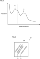
- Fig. 3 is a graph showing a frequency distribution of the above-described phase differences measured within measurement region M (see Fig. 2 ) in single crystal diamond 10.
- the horizontal axis and the vertical axis show a phase difference and a frequency, respectively, and the dashed line along the vertical axis shows the average value of the phase differences.
- This frequency distribution includes: a first peak P1 that exists in a region of values smaller than the average value of the above-described phase differences; and a second peak P2 that exists in a region of values larger than the average value of the above-described phase differences and is smaller in frequency than first peak P1.
- second peak P2 exists in a region of values equal to or greater than 5% of the maximum value of the above-described phase differences, preferably in a region of values equal to or greater than 10% of the maximum value of the above-described phase differences, and more preferably in a region of values equal to or greater than 20% of the maximum value of the above-described phase differences.
- this frequency distribution is not limited to the case where two peaks exist, but three peaks or three or more peaks may exist, for example.
- single crystal diamond 10 is not limited to the case where defect portions 11 are introduced so as to be dispersed at random, but defect portions 11 may be introduced so as to be arranged in a straight line as shown in Fig. 4 , or may be introduced so as to be arranged in an arc line as shown in Fig. 5 .
- straight lines each formed by defect portions 11 arranged in a straight line or arc lines each formed by defect portions 11 arranged in an arc line may be provided at intervals so as to extend side by side. It is to be noted that the number of these straight lines or arc lines is not particularly limited, but may be four as shown in Figs. 4 and 5 , or may be four or more.
- defect portions 11 are introduced into a crystal in a controlled manner such that the maximum value of average values of the phase differences described above is 100 nm or more. Therefore, this single crystal diamond 10 results in a diamond in which occurrence of chipping is suppressed.
- the standard deviation of the phase differences measured within measurement region M is 30 nm or more, as described above.
- defect portions 11 are more uniformly dispersed in single crystal diamond 10 as shown in Fig. 2 . Consequently, occurrence of chipping can be more effectively suppressed in single crystal diamond 10.
- first peak P1 may exist in a region of values smaller than the average value of the above-described phase differences while second peak P2 may exist in a region of values larger than the average value of the above-described phase differences.
- defect portions 11 are further more uniformly dispersed in single crystal diamond 10. Consequently, occurrence of chipping can be more effectively suppressed in single crystal diamond 10.
- the method of manufacturing a single crystal diamond according to the present embodiment will be hereinafter described.
- the steps (S10) to (S50) are sequentially performed, so that single crystal diamond 10 according to the present embodiment can be produced.
- a single crystal substrate preparing step is carried out as step (S10).
- step (S10) referring to Fig. 7 , a single crystal substrate 20 (type: Ib) having a flat plate shape (a square shape) and made of a diamond produced by the high pressure high temperature method is prepared.
- Single crystal substrate 20 has a surface 20a including a (100) plane and a side surface 20b including a (001) plane perpendicular to surface 20a.
- the shape of single crystal substrate 20 is not limited to a square shape as shown in Fig. 7 , but may be a rectangular shape or an octagonal shape, for example.
- a plurality of grooves 21 are provided so as to extend side by side on surface 20a of single crystal substrate 20.
- a distance L between grooves 21 adjacent to each other is more than 10 ⁇ m and not more than 100 ⁇ m, preferably more than 10 ⁇ m and less than 20 ⁇ m, or not less than 20 ⁇ m and not more than 100 ⁇ m.
- groove 21 may be provided, for example, by forming a resist pattern in a line shape on surface 20a using the photolithography method, and then, using plasma to etch surface 20a of single crystal substrate 20 in a portion having no resist pattern formed thereon. Furthermore, groove 21 may be provided by processing surface 20a of single crystal substrate 20 into a line shape using a laser processing machine (grooving process). Furthermore, groove 21 may be provided by mechanically shaving surface 20a of single crystal substrate 20 (mechanical polishing). Furthermore, in this mechanical polishing, a grinding machine having diamond abrasive grains embedded therein; a grinding machine fabricated using cast iron; or a grinding machine fabricated using silicon dioxide (SiO 2 ) can be used, for example.
- grooves 21 each in a line shape can be provided, and a plurality of grooves 21 each formed in a line shape can be arranged in a grid pattern.
- each groove formed in an arc shape or in other shapes can be provided.
- cutting can be carried out by means of laser in the slicing direction. Consequently, height differences can be provided at intervals on surface 20a of single crystal substrate 20. In this way, grooves 21 can be formed in surface 20a of single crystal substrate 20 so as to be appropriately distributed.
- grooves 21 only have to be formed so as to be appropriately distributed in surface 20a, and may be randomly formed.
- more simple methods such as a method using the above-described mechanical polishing and a method of performing heat treatment in an oxygen atmosphere can be employed, for example.
- Fig. 8 shows a height profile on surface 20a of single crystal substrate 20 along a line segment VIII-VIII in Fig. 7 .
- the horizontal direction shows the distance in the direction along surface 20a of single crystal substrate 20 while the vertical direction shows a height.
- a height difference H corresponding to a difference between the minimum height (a portion in which groove 21 is formed) and the maximum height is 15 nm or more, preferably 50 nm or more, and more preferably 300 nm or more.
- surface 20a of single crystal substrate 20 is processed such that distance L between grooves 21 and height difference H fall within the above-described ranges, respectively. Accordingly, in the step (S40) described later, an epitaxial growth layer having defect portions introduced thereinto in a controlled manner can be grown on single crystal substrate 20.
- step (S20) an etching step is carried out as step (S20).
- step (S20) referring to Fig. 7 , surface 20a is etched by reactive ion etching (RIE), for example, using oxygen (O 2 ) gas and carbon tetrafluoride (CF 4 ) gas.
- RIE reactive ion etching
- the etching method is not limited to RIE, but may be sputtering, for example, using argon (Ar) gas as main gas.
- this step (S20) is an extremely important step in the case where surface 20a is processed using a grinding machine having diamond abrasive grains embedded therein.
- a relatively large height difference is provided on surface 20a, so that polishing damage on surface 20a is increased. Consequently, abnormal particles are grown on surface 20a, thereby forming a polycrystal.
- polishing damage on surface 20a is removed by ion etching, formation of a polycrystal caused by growth of abnormal particles can be suppressed.
- polishing damage on surface 20a is reduced when performing: mechanical polishing by a grinding machine fabricated using SiO 2 ; surface cutting by means of laser; or heat treatment in an oxygen atmosphere. Accordingly, the above-described step (S20) can also be omitted.
- step (S30) an ion implantation step is carried out as step (S30).
- step (S30) referring to Fig. 9 , carbon (C) or phosphorus (P) is implanted into single crystal substrate 20 from the surface 20a side. Consequently, a conductive layer 22 is formed in a region including surface 20a.
- an epitaxial growth step is carried out as step (S40).
- step (S40) referring to Fig. 10 , an epitaxial growth layer 23 made of a single crystal diamond is grown on conductive layer 22, for example, by the microwave plasma (MP) CVD method.
- the method of forming epitaxial growth layer 23 is not limited to the MP-CVD method, but may be the hot-filament (HF) CVD method or the DC plasma method, for example.
- epitaxial growth layer 23 grows on the conditions that a growth parameter ( ⁇ ) in a region of 1 ⁇ m to 7 ⁇ m at least in an early stage of growth (a region extending 1 ⁇ m or more and 7 ⁇ m or less from surface 20a in the growth direction) is 2 or more, and the temperature of single crystal substrate 20 is 1050 °C or lower.
- the growth parameter ( ⁇ ) is a value equal to the square root of 3 of the ratio of the growth rate in the ⁇ 100> direction to the growth rate in the ⁇ 111> direction. Accordingly, even when the height difference on surface 20a of single crystal substrate 20 is relatively large, a single crystal diamond (epitaxial growth layer 23) can be grown with stability.
- step (S50) a separation step is carried out as step (S50).
- step (S50) referring to Fig. 11 , conductive layer 22 is electrochemically etched, so that single crystal substrate 20 and epitaxial growth layer 23 are separated. In this way, single crystal diamond 10 (epitaxial growth layer 23) is obtained.
- steps (S10) to (S50) as described above, single crystal diamond 10 is produced, and thus, the method of manufacturing a single crystal diamond according to the present embodiment is completed.
- single crystal diamond 10 was produced by using the method of manufacturing a single crystal diamond according to the present embodiment described above (see Figs. 6 to 11 ).
- step (S10) single crystal substrate 20 having a square shape of 5 mm ⁇ 5 mm and a thickness of 0.7 mm was prepared (see Fig. 7 ).
- height difference H on surface 20a of single crystal substrate 20 was 15 nm or more, and distance L between grooves 21 was more than 10 ⁇ m and not more than 100 ⁇ m (see Fig. 8 ).
- step (S20) single crystal substrate 20 was etched by RIE from surface 20a to a depth region of 0.3 ⁇ m, or etched by sputtering from surface 20a to a depth region of 0.1 ⁇ m (see Fig. 7 ).
- step (S30) carbon ions were implanted with ion implantation energy of 300 keV to 350 keV and at a dose amount of 5 ⁇ 10 15 to 5 ⁇ 10 17 pieces/cm 2 , thereby forming conductive layer 22 (see Fig. 9 ).
- step (S40) epitaxial growth layer 23 having a thickness of 0.7 mm was formed (see Fig. 10 ).
- hydrogen (H 2 ) gas, methane (CH 4 ) gas and nitrogen (N 2 ) gas the concentration of CH 4 gas to H 2 gas was set at 5% to 20%, and the concentration of N 2 gas to CH 4 gas was set at 0.5% to 4%.
- the pressure was also set at 9.3 kPa to 14.7 kPa, and the substrate temperature was set at 800 °C to 1100 °C.
- the size of single crystal diamond 10 was 1 mm ⁇ 1 mm, 3 mm ⁇ 3 mm, or 6 mm ⁇ 6 mm. In this way, single crystal diamonds 10 in Examples 1 to 6 were produced. Also, as Comparative Examples 1 to 3, single crystal diamonds were produced such that height difference H and distance L between grooves 21 on surface 20a of single crystal substrate 20 were beyond the above-described ranges, respectively.
- the growth surfaces of the single crystal diamonds in Examples 1 to 6 and Comparative Examples 1 to 3 were polished, and then, the phase differences were measured.
- Each phase difference was measured using a birefringence distribution measurement apparatus (WPA-100 manufactured by Photonic Lattice, Inc.) and defining a plurality of measurement regions M (1 mm ⁇ 1 mm) within main surface 10a of single crystal diamond 10 as described above (see Fig. 2 ).
- WPA-100 manufactured by Photonic Lattice, Inc.
- the above-described measurement apparatus was adjusted using a lens such that information in an area of 20 ⁇ m ⁇ 20 ⁇ m could be obtained from a sample (a single crystal diamond). It is to be noted that the above-described measurement apparatus allows measurement in a range of phase differences of 0 nm to 3000 nm using three types of wavelengths (523 nm, 543 nm, and 575 nm).
- the feed rate was set at 0.05 mm/blade, 0.1 mm /blade, or 0.15 mm/blade.
- an aluminum material A5052 was used as a workpiece. After the workpiece was subjected to cutting work on the above-described conditions, it was examined whether chipping occurred or not in each diamond. Furthermore, the surface roughness ( ⁇ m) of the workpiece and occurrence of burrs were also examined on each of the feed rate conditions (mm/blade).
- Tables 1 and 2 and Figs. 12 to 14 The above-described experimental results are shown in Tables 1 and 2 and Figs. 12 to 14 .
- Table 1 shows the results about phase difference measurement; the examination results about occurrence of chipping during cutting edge polishing processing; and the examination results about occurrence of chipping after cutting work.
- Table 2 shows the examination results about occurrence of burrs after cutting work.
- Figs. 12 and 13 each show a photograph of birefringence in a single crystal diamond in each of Examples 1 to 6 and Comparative Examples 1 to 3. Furthermore, Fig.
- FIG. 14 is a graph showing the relation between the feed rate (mm/blade) and the surface roughness ( ⁇ m) of the workpiece, in which the horizontal axis shows the feed rate (mm/blade) while the vertical axis shows the surface roughness ( ⁇ m) of the workpiece.
- the maximum value of average values of the phase differences was 30 nm or more in each of Reference Examples 1 to 4, and 100 nm or more in Examples 5 and 6, whereas the maximum value of average values of the phase differences was less than 30 nm in each of Comparative Examples 1 to 3. Furthermore, the phase differences were measured using a wavelength of 543 nm, and each maximum value of the phase differences was 2000 nm or less. It was found from these results that height difference H on the surface of a single crystal substrate is set at 15 nm or more, and distance L between grooves 21 is set at more than 10 ⁇ m and 100 ⁇ m or less, which leads to 30 nm or more of the maximum value of average values of the phase differences in the single crystal diamond formed on the single crystal substrate.
- the single crystal diamond and the diamond tool according to the present invention can be particularly advantageously applied to a single crystal diamond for which occurrence of chipping needs to be suppressed and a diamond tool that needs to be improved in durability.
Landscapes
- Chemical & Material Sciences (AREA)
- Engineering & Computer Science (AREA)
- Crystallography & Structural Chemistry (AREA)
- Materials Engineering (AREA)
- Metallurgy (AREA)
- Organic Chemistry (AREA)
- Chemical Kinetics & Catalysis (AREA)
- General Chemical & Material Sciences (AREA)
- Crystals, And After-Treatments Of Crystals (AREA)
- Chemical Vapour Deposition (AREA)
- Carbon And Carbon Compounds (AREA)
Claims (8)
- Einkristall-Diamant, in den ein Defektbereich eingebracht ist,wobei der Einkristall-Diamant in einem Bereich, in den der Defektbereich eingebracht ist, einen Doppelbrechungsindex aufweist, der unterschiedliche Brechungsindizes in Abhängigkeit von der Richtung verhindert,der Defektbereich durch eine Phasendifferenz erkannt werden kann, die auftritt, wenn der Einkristall-Diamant mit zirkular polarisiertem Licht bestrahlt wird,die Phasendifferenz mit Hilfe einer Vorrichtung zur Messung der Doppelbrechungsverteilung unter Verwendung eines integrierten Wellenlängenplattenschemas gemessen wird,die Vorrichtung zur Messung der Doppelbrechungsverteilung die Messung in einem Bereich von Phasendifferenzen von 0 nm bis 3000 nm unter Verwendung von drei Arten von Wellenlängen, nämlich 523 nm, 543 nm und 575 nm, ermöglicht undein Maximalwert von Durchschnittswerten der Phasendifferenzen, gemessen in Bezug auf eine Dicke von 700 µm innerhalb einer Vielzahl von Messbereichen, 100nm oder mehr beträgt, wobei jeder der Vielzahl von Messbereichen in Form eines Quadrats mit einer Seitenlänge von 1 mm ausgebildet ist, wobei jeder der Durchschnittswerte ein Durchschnittswert in einem entsprechenden der Vielzahl von Messbereichen ist,dadurch gekennzeichnet, dasseine Standardabweichung der in einem der Messbereich gemessenen Phasendifferenzen 30 nm oder mehr beträgt.
- Einkristall-Diamant nach Anspruch 1, wobei eine Vielzahl von Peaks in einer Frequenzverteilung der in einem der mehreren Messbereichen gemessen Phasendifferenzen existiert.
- Einkristall-Diamant nach Anspruch 2, wobei ein erster Peak in einem Bereich mit Werten, die kleiner als der Durchschnittswert der Phasendifferenzen sind, und ein zweiter Peak in einem Bereich mit Werten, die größer als der Durchschnittswert der Phasendifferenzen sind, in der Frequenzverteilung der in einem der mehreren Messbereiche gemessenen Phasendifferenzen vorhanden sind.
- Einkristall-Diamant nach einem der Ansprüche 1 bis 3, wobei die Defektbereiche so eingebracht sind, dass sie in einer geraden Linie angeordnet sind.
- Einkristall-Diamant nach einem der Ansprüche 1 bis 4, wobei die Defektabschnitte so eingebracht sind, dass sie in einer Bogenlinie angeordnet sind.
- Einkristall-Diamant nach einem der Ansprüche 1 bis 5, hergestellt durch ein Dampfphasen-Syntheseverfahren.
- Einkristall-Diamant nach einem der Ansprüche 1 bis 6, verwendet für ein Diamantwerkzeug.
- Diamantwerkzeug, umfassend den Einkristall-Diamanten nach einem der Ansprüche 1 bis 7.
Applications Claiming Priority (2)
| Application Number | Priority Date | Filing Date | Title |
|---|---|---|---|
| JP2013081157 | 2013-04-09 | ||
| PCT/JP2014/059713 WO2014168053A1 (ja) | 2013-04-09 | 2014-04-02 | 単結晶ダイヤモンドおよびダイヤモンド工具 |
Publications (3)
| Publication Number | Publication Date |
|---|---|
| EP2985368A1 EP2985368A1 (de) | 2016-02-17 |
| EP2985368A4 EP2985368A4 (de) | 2016-12-14 |
| EP2985368B1 true EP2985368B1 (de) | 2023-08-30 |
Family
ID=51689463
Family Applications (1)
| Application Number | Title | Priority Date | Filing Date |
|---|---|---|---|
| EP14783086.3A Active EP2985368B1 (de) | 2013-04-09 | 2014-04-02 | Einkristalliner diamant und diamantwerkzeug |
Country Status (5)
| Country | Link |
|---|---|
| US (1) | US9963801B2 (de) |
| EP (1) | EP2985368B1 (de) |
| JP (1) | JP6360041B2 (de) |
| CN (1) | CN104603335B (de) |
| WO (1) | WO2014168053A1 (de) |
Families Citing this family (9)
| Publication number | Priority date | Publication date | Assignee | Title |
|---|---|---|---|---|
| JPWO2014178281A1 (ja) * | 2013-04-30 | 2017-02-23 | 住友電気工業株式会社 | 単結晶ダイヤモンドおよびダイヤモンド工具 |
| KR102392424B1 (ko) * | 2014-07-22 | 2022-05-02 | 스미토모덴키고교가부시키가이샤 | 단결정 다이아몬드 및 그 제조 방법, 단결정 다이아몬드를 포함하는 공구, 및 단결정 다이아몬드를 포함하는 부품 |
| US11001938B2 (en) | 2014-08-11 | 2021-05-11 | Sumitomo Electric Industries, Ltd. | Diamond composite body, substrate, diamond, tool including diamond, and method for manufacturing diamond |
| GB201620413D0 (en) | 2016-12-01 | 2017-01-18 | Element Six Tech Ltd | Single crystal synthetic diamond material via chemical vapour deposition |
| WO2021065258A1 (ja) * | 2019-10-01 | 2021-04-08 | 住友電工ハードメタル株式会社 | ダイヤモンド棒状体、ダイヤモンド工具およびカンチレバー |
| CN111996581B (zh) * | 2020-07-08 | 2021-10-26 | 西安电子科技大学 | 一种单晶金刚石与衬底无损耗快速分离方法 |
| EP4269004B1 (de) * | 2020-12-24 | 2024-10-23 | Sumitomo Electric Hardmetal Corp. | Verfahren zur herstellung eines diamantwerkzeugzwischenprodukts und verfahren zur bestimmung eines einkristalldiamants |
| JPWO2022210566A1 (de) | 2021-03-31 | 2022-10-06 | ||
| JPWO2022209512A1 (de) * | 2021-03-31 | 2022-10-06 |
Family Cites Families (16)
| Publication number | Priority date | Publication date | Assignee | Title |
|---|---|---|---|---|
| US4316385A (en) * | 1980-06-18 | 1982-02-23 | General Electric Company | Fingerprinting crystals |
| CZ302228B6 (cs) | 2000-06-15 | 2011-01-05 | Element Six (Pty) Ltd | Monokrystalická diamantová vrstva pripravená chemickým vylucováním z plynné fáze |
| GB0221949D0 (en) | 2002-09-20 | 2002-10-30 | Diamanx Products Ltd | Single crystal diamond |
| GB0227261D0 (en) | 2002-11-21 | 2002-12-31 | Element Six Ltd | Optical quality diamond material |
| GB0303860D0 (en) | 2003-02-19 | 2003-03-26 | Element Six Ltd | CVD diamond in wear applications |
| JP4623356B2 (ja) | 2003-12-02 | 2011-02-02 | 住友電気工業株式会社 | 単結晶ダイヤモンド |
| JP4697514B2 (ja) * | 2004-01-16 | 2011-06-08 | 住友電気工業株式会社 | ダイヤモンド単結晶基板の製造方法およびダイヤモンド単結晶基板 |
| US7481879B2 (en) | 2004-01-16 | 2009-01-27 | Sumitomo Electric Industries, Ltd. | Diamond single crystal substrate manufacturing method and diamond single crystal substrate |
| JP2006062923A (ja) * | 2004-08-27 | 2006-03-09 | Sumitomo Electric Ind Ltd | ダイヤモンドドーム部品およびその製造方法 |
| WO2006048957A1 (ja) * | 2004-11-05 | 2006-05-11 | Sumitomo Electric Industries, Ltd. | 単結晶ダイヤモンド |
| JP5002982B2 (ja) * | 2005-04-15 | 2012-08-15 | 住友電気工業株式会社 | 単結晶ダイヤモンドの製造方法 |
| JP5594613B2 (ja) * | 2005-04-15 | 2014-09-24 | 住友電気工業株式会社 | 単結晶ダイヤモンドおよびその製造方法 |
| US9133566B2 (en) | 2005-12-09 | 2015-09-15 | Element Six Technologies Limited | High crystalline quality synthetic diamond |
| DE602006021467D1 (de) | 2005-12-09 | 2011-06-01 | Element Six Technologies Pty Ltd | Synthetischer diamant mit hoher kristalliner qualität |
| JP2007230807A (ja) * | 2006-02-28 | 2007-09-13 | Allied Material Corp | ダイヤモンド製品の製造方法 |
| GB2476306B (en) * | 2009-12-21 | 2012-07-11 | Element Six Ltd | Single crystal diamond material |
-
2014
- 2014-04-02 JP JP2015511223A patent/JP6360041B2/ja active Active
- 2014-04-02 US US14/423,884 patent/US9963801B2/en active Active
- 2014-04-02 CN CN201480002248.XA patent/CN104603335B/zh active Active
- 2014-04-02 EP EP14783086.3A patent/EP2985368B1/de active Active
- 2014-04-02 WO PCT/JP2014/059713 patent/WO2014168053A1/ja not_active Ceased
Also Published As
| Publication number | Publication date |
|---|---|
| EP2985368A1 (de) | 2016-02-17 |
| WO2014168053A1 (ja) | 2014-10-16 |
| EP2985368A4 (de) | 2016-12-14 |
| US20150191850A1 (en) | 2015-07-09 |
| JP6360041B2 (ja) | 2018-07-18 |
| CN104603335A (zh) | 2015-05-06 |
| US9963801B2 (en) | 2018-05-08 |
| CN104603335B (zh) | 2017-10-17 |
| JPWO2014168053A1 (ja) | 2017-02-16 |
Similar Documents
| Publication | Publication Date | Title |
|---|---|---|
| EP2985368B1 (de) | Einkristalliner diamant und diamantwerkzeug | |
| JP6665952B2 (ja) | 単結晶ダイヤモンド工具及び単結晶ダイヤモンド工具の製造方法 | |
| KR102407952B1 (ko) | 단결정 다이아몬드, 단결정 다이아몬드의 제조 방법 및 단결정 다이아몬드를 이용한 공구 | |
| EP3173510B1 (de) | Verfahren zur herstellung von einkristallinem diamant | |
| US12139813B2 (en) | SiC wafer and manufacturing method for SiC wafer | |
| WO2017014311A1 (ja) | 単結晶ダイヤモンド材、単結晶ダイヤモンドチップおよび穿孔工具 | |
| EP2848716B1 (de) | Einkristalliner diamant und diamantwerkzeug | |
| JPWO2019059123A1 (ja) | 単結晶ダイヤモンドおよびその製造方法 | |
| JP4697514B2 (ja) | ダイヤモンド単結晶基板の製造方法およびダイヤモンド単結晶基板 |
Legal Events
| Date | Code | Title | Description |
|---|---|---|---|
| PUAI | Public reference made under article 153(3) epc to a published international application that has entered the european phase |
Free format text: ORIGINAL CODE: 0009012 |
|
| 17P | Request for examination filed |
Effective date: 20150220 |
|
| AK | Designated contracting states |
Kind code of ref document: A1 Designated state(s): AL AT BE BG CH CY CZ DE DK EE ES FI FR GB GR HR HU IE IS IT LI LT LU LV MC MK MT NL NO PL PT RO RS SE SI SK SM TR |
|
| AX | Request for extension of the european patent |
Extension state: BA ME |
|
| DAX | Request for extension of the european patent (deleted) | ||
| A4 | Supplementary search report drawn up and despatched |
Effective date: 20161115 |
|
| RIC1 | Information provided on ipc code assigned before grant |
Ipc: C30B 25/10 20060101ALI20161109BHEP Ipc: C30B 25/00 20060101ALI20161109BHEP Ipc: C30B 29/04 20060101AFI20161109BHEP |
|
| STAA | Information on the status of an ep patent application or granted ep patent |
Free format text: STATUS: EXAMINATION IS IN PROGRESS |
|
| 17Q | First examination report despatched |
Effective date: 20190923 |
|
| GRAP | Despatch of communication of intention to grant a patent |
Free format text: ORIGINAL CODE: EPIDOSNIGR1 |
|
| STAA | Information on the status of an ep patent application or granted ep patent |
Free format text: STATUS: GRANT OF PATENT IS INTENDED |
|
| INTG | Intention to grant announced |
Effective date: 20230324 |
|
| GRAS | Grant fee paid |
Free format text: ORIGINAL CODE: EPIDOSNIGR3 |
|
| GRAA | (expected) grant |
Free format text: ORIGINAL CODE: 0009210 |
|
| STAA | Information on the status of an ep patent application or granted ep patent |
Free format text: STATUS: THE PATENT HAS BEEN GRANTED |
|
| AK | Designated contracting states |
Kind code of ref document: B1 Designated state(s): AL AT BE BG CH CY CZ DE DK EE ES FI FR GB GR HR HU IE IS IT LI LT LU LV MC MK MT NL NO PL PT RO RS SE SI SK SM TR |
|
| P01 | Opt-out of the competence of the unified patent court (upc) registered |
Effective date: 20230721 |
|
| REG | Reference to a national code |
Ref country code: GB Ref legal event code: FG4D |
|
| REG | Reference to a national code |
Ref country code: CH Ref legal event code: EP |
|
| REG | Reference to a national code |
Ref country code: DE Ref legal event code: R096 Ref document number: 602014088117 Country of ref document: DE |
|
| REG | Reference to a national code |
Ref country code: IE Ref legal event code: FG4D |
|
| REG | Reference to a national code |
Ref country code: LT Ref legal event code: MG9D |
|
| REG | Reference to a national code |
Ref country code: NL Ref legal event code: MP Effective date: 20230830 |
|
| REG | Reference to a national code |
Ref country code: AT Ref legal event code: MK05 Ref document number: 1605552 Country of ref document: AT Kind code of ref document: T Effective date: 20230830 |
|
| PG25 | Lapsed in a contracting state [announced via postgrant information from national office to epo] |
Ref country code: GR Free format text: LAPSE BECAUSE OF FAILURE TO SUBMIT A TRANSLATION OF THE DESCRIPTION OR TO PAY THE FEE WITHIN THE PRESCRIBED TIME-LIMIT Effective date: 20231201 |
|
| PG25 | Lapsed in a contracting state [announced via postgrant information from national office to epo] |
Ref country code: IS Free format text: LAPSE BECAUSE OF FAILURE TO SUBMIT A TRANSLATION OF THE DESCRIPTION OR TO PAY THE FEE WITHIN THE PRESCRIBED TIME-LIMIT Effective date: 20231230 |
|
| PG25 | Lapsed in a contracting state [announced via postgrant information from national office to epo] |
Ref country code: SE Free format text: LAPSE BECAUSE OF FAILURE TO SUBMIT A TRANSLATION OF THE DESCRIPTION OR TO PAY THE FEE WITHIN THE PRESCRIBED TIME-LIMIT Effective date: 20230830 Ref country code: RS Free format text: LAPSE BECAUSE OF FAILURE TO SUBMIT A TRANSLATION OF THE DESCRIPTION OR TO PAY THE FEE WITHIN THE PRESCRIBED TIME-LIMIT Effective date: 20230830 Ref country code: NO Free format text: LAPSE BECAUSE OF FAILURE TO SUBMIT A TRANSLATION OF THE DESCRIPTION OR TO PAY THE FEE WITHIN THE PRESCRIBED TIME-LIMIT Effective date: 20231130 Ref country code: LV Free format text: LAPSE BECAUSE OF FAILURE TO SUBMIT A TRANSLATION OF THE DESCRIPTION OR TO PAY THE FEE WITHIN THE PRESCRIBED TIME-LIMIT Effective date: 20230830 Ref country code: LT Free format text: LAPSE BECAUSE OF FAILURE TO SUBMIT A TRANSLATION OF THE DESCRIPTION OR TO PAY THE FEE WITHIN THE PRESCRIBED TIME-LIMIT Effective date: 20230830 Ref country code: IS Free format text: LAPSE BECAUSE OF FAILURE TO SUBMIT A TRANSLATION OF THE DESCRIPTION OR TO PAY THE FEE WITHIN THE PRESCRIBED TIME-LIMIT Effective date: 20231230 Ref country code: HR Free format text: LAPSE BECAUSE OF FAILURE TO SUBMIT A TRANSLATION OF THE DESCRIPTION OR TO PAY THE FEE WITHIN THE PRESCRIBED TIME-LIMIT Effective date: 20230830 Ref country code: GR Free format text: LAPSE BECAUSE OF FAILURE TO SUBMIT A TRANSLATION OF THE DESCRIPTION OR TO PAY THE FEE WITHIN THE PRESCRIBED TIME-LIMIT Effective date: 20231201 Ref country code: FI Free format text: LAPSE BECAUSE OF FAILURE TO SUBMIT A TRANSLATION OF THE DESCRIPTION OR TO PAY THE FEE WITHIN THE PRESCRIBED TIME-LIMIT Effective date: 20230830 Ref country code: AT Free format text: LAPSE BECAUSE OF FAILURE TO SUBMIT A TRANSLATION OF THE DESCRIPTION OR TO PAY THE FEE WITHIN THE PRESCRIBED TIME-LIMIT Effective date: 20230830 |
|
| PG25 | Lapsed in a contracting state [announced via postgrant information from national office to epo] |
Ref country code: PL Free format text: LAPSE BECAUSE OF FAILURE TO SUBMIT A TRANSLATION OF THE DESCRIPTION OR TO PAY THE FEE WITHIN THE PRESCRIBED TIME-LIMIT Effective date: 20230830 Ref country code: NL Free format text: LAPSE BECAUSE OF FAILURE TO SUBMIT A TRANSLATION OF THE DESCRIPTION OR TO PAY THE FEE WITHIN THE PRESCRIBED TIME-LIMIT Effective date: 20230830 |
|
| PG25 | Lapsed in a contracting state [announced via postgrant information from national office to epo] |
Ref country code: ES Free format text: LAPSE BECAUSE OF FAILURE TO SUBMIT A TRANSLATION OF THE DESCRIPTION OR TO PAY THE FEE WITHIN THE PRESCRIBED TIME-LIMIT Effective date: 20230830 |
|
| PG25 | Lapsed in a contracting state [announced via postgrant information from national office to epo] |
Ref country code: SM Free format text: LAPSE BECAUSE OF FAILURE TO SUBMIT A TRANSLATION OF THE DESCRIPTION OR TO PAY THE FEE WITHIN THE PRESCRIBED TIME-LIMIT Effective date: 20230830 Ref country code: RO Free format text: LAPSE BECAUSE OF FAILURE TO SUBMIT A TRANSLATION OF THE DESCRIPTION OR TO PAY THE FEE WITHIN THE PRESCRIBED TIME-LIMIT Effective date: 20230830 Ref country code: ES Free format text: LAPSE BECAUSE OF FAILURE TO SUBMIT A TRANSLATION OF THE DESCRIPTION OR TO PAY THE FEE WITHIN THE PRESCRIBED TIME-LIMIT Effective date: 20230830 Ref country code: EE Free format text: LAPSE BECAUSE OF FAILURE TO SUBMIT A TRANSLATION OF THE DESCRIPTION OR TO PAY THE FEE WITHIN THE PRESCRIBED TIME-LIMIT Effective date: 20230830 Ref country code: DK Free format text: LAPSE BECAUSE OF FAILURE TO SUBMIT A TRANSLATION OF THE DESCRIPTION OR TO PAY THE FEE WITHIN THE PRESCRIBED TIME-LIMIT Effective date: 20230830 Ref country code: CZ Free format text: LAPSE BECAUSE OF FAILURE TO SUBMIT A TRANSLATION OF THE DESCRIPTION OR TO PAY THE FEE WITHIN THE PRESCRIBED TIME-LIMIT Effective date: 20230830 Ref country code: PT Free format text: LAPSE BECAUSE OF FAILURE TO SUBMIT A TRANSLATION OF THE DESCRIPTION OR TO PAY THE FEE WITHIN THE PRESCRIBED TIME-LIMIT Effective date: 20240102 Ref country code: SK Free format text: LAPSE BECAUSE OF FAILURE TO SUBMIT A TRANSLATION OF THE DESCRIPTION OR TO PAY THE FEE WITHIN THE PRESCRIBED TIME-LIMIT Effective date: 20230830 |
|
| PG25 | Lapsed in a contracting state [announced via postgrant information from national office to epo] |
Ref country code: IT Free format text: LAPSE BECAUSE OF FAILURE TO SUBMIT A TRANSLATION OF THE DESCRIPTION OR TO PAY THE FEE WITHIN THE PRESCRIBED TIME-LIMIT Effective date: 20230830 |
|
| REG | Reference to a national code |
Ref country code: DE Ref legal event code: R097 Ref document number: 602014088117 Country of ref document: DE |
|
| PLBE | No opposition filed within time limit |
Free format text: ORIGINAL CODE: 0009261 |
|
| STAA | Information on the status of an ep patent application or granted ep patent |
Free format text: STATUS: NO OPPOSITION FILED WITHIN TIME LIMIT |
|
| PG25 | Lapsed in a contracting state [announced via postgrant information from national office to epo] |
Ref country code: SI Free format text: LAPSE BECAUSE OF FAILURE TO SUBMIT A TRANSLATION OF THE DESCRIPTION OR TO PAY THE FEE WITHIN THE PRESCRIBED TIME-LIMIT Effective date: 20230830 |
|
| 26N | No opposition filed |
Effective date: 20240603 |
|
| PG25 | Lapsed in a contracting state [announced via postgrant information from national office to epo] |
Ref country code: BG Free format text: LAPSE BECAUSE OF FAILURE TO SUBMIT A TRANSLATION OF THE DESCRIPTION OR TO PAY THE FEE WITHIN THE PRESCRIBED TIME-LIMIT Effective date: 20230830 |
|
| PG25 | Lapsed in a contracting state [announced via postgrant information from national office to epo] |
Ref country code: MC Free format text: LAPSE BECAUSE OF FAILURE TO SUBMIT A TRANSLATION OF THE DESCRIPTION OR TO PAY THE FEE WITHIN THE PRESCRIBED TIME-LIMIT Effective date: 20230830 |
|
| PG25 | Lapsed in a contracting state [announced via postgrant information from national office to epo] |
Ref country code: MC Free format text: LAPSE BECAUSE OF FAILURE TO SUBMIT A TRANSLATION OF THE DESCRIPTION OR TO PAY THE FEE WITHIN THE PRESCRIBED TIME-LIMIT Effective date: 20230830 Ref country code: BG Free format text: LAPSE BECAUSE OF FAILURE TO SUBMIT A TRANSLATION OF THE DESCRIPTION OR TO PAY THE FEE WITHIN THE PRESCRIBED TIME-LIMIT Effective date: 20230830 |
|
| REG | Reference to a national code |
Ref country code: CH Ref legal event code: PL |
|
| PG25 | Lapsed in a contracting state [announced via postgrant information from national office to epo] |
Ref country code: LU Free format text: LAPSE BECAUSE OF NON-PAYMENT OF DUE FEES Effective date: 20240402 |
|
| REG | Reference to a national code |
Ref country code: BE Ref legal event code: MM Effective date: 20240430 |
|
| PG25 | Lapsed in a contracting state [announced via postgrant information from national office to epo] |
Ref country code: LU Free format text: LAPSE BECAUSE OF NON-PAYMENT OF DUE FEES Effective date: 20240402 |
|
| PG25 | Lapsed in a contracting state [announced via postgrant information from national office to epo] |
Ref country code: BE Free format text: LAPSE BECAUSE OF NON-PAYMENT OF DUE FEES Effective date: 20240430 |
|
| PG25 | Lapsed in a contracting state [announced via postgrant information from national office to epo] |
Ref country code: FR Free format text: LAPSE BECAUSE OF NON-PAYMENT OF DUE FEES Effective date: 20240430 |
|
| PG25 | Lapsed in a contracting state [announced via postgrant information from national office to epo] |
Ref country code: FR Free format text: LAPSE BECAUSE OF NON-PAYMENT OF DUE FEES Effective date: 20240430 Ref country code: BE Free format text: LAPSE BECAUSE OF NON-PAYMENT OF DUE FEES Effective date: 20240430 Ref country code: CH Free format text: LAPSE BECAUSE OF NON-PAYMENT OF DUE FEES Effective date: 20240430 |
|
| PG25 | Lapsed in a contracting state [announced via postgrant information from national office to epo] |
Ref country code: IE Free format text: LAPSE BECAUSE OF NON-PAYMENT OF DUE FEES Effective date: 20240402 |
|
| PGFP | Annual fee paid to national office [announced via postgrant information from national office to epo] |
Ref country code: DE Payment date: 20250305 Year of fee payment: 12 |
|
| PG25 | Lapsed in a contracting state [announced via postgrant information from national office to epo] |
Ref country code: CY Free format text: LAPSE BECAUSE OF FAILURE TO SUBMIT A TRANSLATION OF THE DESCRIPTION OR TO PAY THE FEE WITHIN THE PRESCRIBED TIME-LIMIT; INVALID AB INITIO Effective date: 20140402 |
|
| PG25 | Lapsed in a contracting state [announced via postgrant information from national office to epo] |
Ref country code: HU Free format text: LAPSE BECAUSE OF FAILURE TO SUBMIT A TRANSLATION OF THE DESCRIPTION OR TO PAY THE FEE WITHIN THE PRESCRIBED TIME-LIMIT; INVALID AB INITIO Effective date: 20140402 |
|
| PG25 | Lapsed in a contracting state [announced via postgrant information from national office to epo] |
Ref country code: TR Free format text: LAPSE BECAUSE OF FAILURE TO SUBMIT A TRANSLATION OF THE DESCRIPTION OR TO PAY THE FEE WITHIN THE PRESCRIBED TIME-LIMIT Effective date: 20230830 |
|
| PGFP | Annual fee paid to national office [announced via postgrant information from national office to epo] |
Ref country code: GB Payment date: 20260313 Year of fee payment: 13 |