EP2985643A1 - Plaque de guidage de lumière et procédé de fabrication de celle-ci, et dispositif d'affichage comportant celle-ci - Google Patents
Plaque de guidage de lumière et procédé de fabrication de celle-ci, et dispositif d'affichage comportant celle-ci Download PDFInfo
- Publication number
- EP2985643A1 EP2985643A1 EP13861500.0A EP13861500A EP2985643A1 EP 2985643 A1 EP2985643 A1 EP 2985643A1 EP 13861500 A EP13861500 A EP 13861500A EP 2985643 A1 EP2985643 A1 EP 2985643A1
- Authority
- EP
- European Patent Office
- Prior art keywords
- groove
- light guide
- guide plate
- forming
- manufacturing
- Prior art date
- Legal status (The legal status is an assumption and is not a legal conclusion. Google has not performed a legal analysis and makes no representation as to the accuracy of the status listed.)
- Granted
Links
- 238000004519 manufacturing process Methods 0.000 title claims abstract description 35
- 239000010410 layer Substances 0.000 claims abstract description 80
- 238000000034 method Methods 0.000 claims abstract description 31
- 239000011241 protective layer Substances 0.000 claims abstract description 23
- 239000000758 substrate Substances 0.000 claims abstract description 23
- 239000000463 material Substances 0.000 claims description 40
- 229920002120 photoresistant polymer Polymers 0.000 claims description 40
- 238000004380 ashing Methods 0.000 claims description 2
- 239000004973 liquid crystal related substance Substances 0.000 description 7
- 239000011248 coating agent Substances 0.000 description 3
- 238000000576 coating method Methods 0.000 description 3
- 230000000694 effects Effects 0.000 description 3
- 238000005530 etching Methods 0.000 description 3
- 230000003287 optical effect Effects 0.000 description 3
- KRHYYFGTRYWZRS-UHFFFAOYSA-N Fluorane Chemical compound F KRHYYFGTRYWZRS-UHFFFAOYSA-N 0.000 description 2
- 230000005540 biological transmission Effects 0.000 description 2
- 239000011521 glass Substances 0.000 description 2
- 238000000059 patterning Methods 0.000 description 2
- 230000001681 protective effect Effects 0.000 description 2
- 239000010453 quartz Substances 0.000 description 2
- VYPSYNLAJGMNEJ-UHFFFAOYSA-N silicon dioxide Inorganic materials O=[Si]=O VYPSYNLAJGMNEJ-UHFFFAOYSA-N 0.000 description 2
- 238000004544 sputter deposition Methods 0.000 description 2
- 238000009826 distribution Methods 0.000 description 1
- 238000005286 illumination Methods 0.000 description 1
- 239000002184 metal Substances 0.000 description 1
- 238000012986 modification Methods 0.000 description 1
- 230000004048 modification Effects 0.000 description 1
- 239000007787 solid Substances 0.000 description 1
- 230000000153 supplemental effect Effects 0.000 description 1
- 238000009827 uniform distribution Methods 0.000 description 1
Images


Classifications
-
- G—PHYSICS
- G02—OPTICS
- G02B—OPTICAL ELEMENTS, SYSTEMS OR APPARATUS
- G02B6/00—Light guides; Structural details of arrangements comprising light guides and other optical elements, e.g. couplings
- G02B6/0001—Light guides; Structural details of arrangements comprising light guides and other optical elements, e.g. couplings specially adapted for lighting devices or systems
- G02B6/0011—Light guides; Structural details of arrangements comprising light guides and other optical elements, e.g. couplings specially adapted for lighting devices or systems the light guides being planar or of plate-like form
- G02B6/0033—Means for improving the coupling-out of light from the light guide
- G02B6/0058—Means for improving the coupling-out of light from the light guide varying in density, size, shape or depth along the light guide
-
- B—PERFORMING OPERATIONS; TRANSPORTING
- B29—WORKING OF PLASTICS; WORKING OF SUBSTANCES IN A PLASTIC STATE IN GENERAL
- B29D—PRODUCING PARTICULAR ARTICLES FROM PLASTICS OR FROM SUBSTANCES IN A PLASTIC STATE
- B29D11/00—Producing optical elements, e.g. lenses or prisms
- B29D11/00663—Production of light guides
-
- G—PHYSICS
- G02—OPTICS
- G02B—OPTICAL ELEMENTS, SYSTEMS OR APPARATUS
- G02B1/00—Optical elements characterised by the material of which they are made; Optical coatings for optical elements
- G02B1/10—Optical coatings produced by application to, or surface treatment of, optical elements
- G02B1/11—Anti-reflection coatings
-
- G—PHYSICS
- G02—OPTICS
- G02B—OPTICAL ELEMENTS, SYSTEMS OR APPARATUS
- G02B6/00—Light guides; Structural details of arrangements comprising light guides and other optical elements, e.g. couplings
- G02B6/0001—Light guides; Structural details of arrangements comprising light guides and other optical elements, e.g. couplings specially adapted for lighting devices or systems
- G02B6/0011—Light guides; Structural details of arrangements comprising light guides and other optical elements, e.g. couplings specially adapted for lighting devices or systems the light guides being planar or of plate-like form
- G02B6/0033—Means for improving the coupling-out of light from the light guide
- G02B6/0035—Means for improving the coupling-out of light from the light guide provided on the surface of the light guide or in the bulk of it
- G02B6/0036—2-D arrangement of prisms, protrusions, indentations or roughened surfaces
-
- G—PHYSICS
- G02—OPTICS
- G02B—OPTICAL ELEMENTS, SYSTEMS OR APPARATUS
- G02B6/00—Light guides; Structural details of arrangements comprising light guides and other optical elements, e.g. couplings
- G02B6/0001—Light guides; Structural details of arrangements comprising light guides and other optical elements, e.g. couplings specially adapted for lighting devices or systems
- G02B6/0011—Light guides; Structural details of arrangements comprising light guides and other optical elements, e.g. couplings specially adapted for lighting devices or systems the light guides being planar or of plate-like form
- G02B6/0033—Means for improving the coupling-out of light from the light guide
- G02B6/005—Means for improving the coupling-out of light from the light guide provided by one optical element, or plurality thereof, placed on the light output side of the light guide
- G02B6/0055—Reflecting element, sheet or layer
-
- G—PHYSICS
- G02—OPTICS
- G02B—OPTICAL ELEMENTS, SYSTEMS OR APPARATUS
- G02B6/00—Light guides; Structural details of arrangements comprising light guides and other optical elements, e.g. couplings
- G02B6/0001—Light guides; Structural details of arrangements comprising light guides and other optical elements, e.g. couplings specially adapted for lighting devices or systems
- G02B6/0011—Light guides; Structural details of arrangements comprising light guides and other optical elements, e.g. couplings specially adapted for lighting devices or systems the light guides being planar or of plate-like form
- G02B6/0033—Means for improving the coupling-out of light from the light guide
- G02B6/0063—Means for improving the coupling-out of light from the light guide for extracting light out both the major surfaces of the light guide
-
- G—PHYSICS
- G02—OPTICS
- G02B—OPTICAL ELEMENTS, SYSTEMS OR APPARATUS
- G02B6/00—Light guides; Structural details of arrangements comprising light guides and other optical elements, e.g. couplings
- G02B6/0001—Light guides; Structural details of arrangements comprising light guides and other optical elements, e.g. couplings specially adapted for lighting devices or systems
- G02B6/0011—Light guides; Structural details of arrangements comprising light guides and other optical elements, e.g. couplings specially adapted for lighting devices or systems the light guides being planar or of plate-like form
- G02B6/0065—Manufacturing aspects; Material aspects
-
- G—PHYSICS
- G02—OPTICS
- G02B—OPTICAL ELEMENTS, SYSTEMS OR APPARATUS
- G02B6/00—Light guides; Structural details of arrangements comprising light guides and other optical elements, e.g. couplings
- G02B6/0001—Light guides; Structural details of arrangements comprising light guides and other optical elements, e.g. couplings specially adapted for lighting devices or systems
- G02B6/0011—Light guides; Structural details of arrangements comprising light guides and other optical elements, e.g. couplings specially adapted for lighting devices or systems the light guides being planar or of plate-like form
- G02B6/0075—Arrangements of multiple light guides
- G02B6/0076—Stacked arrangements of multiple light guides of the same or different cross-sectional area
-
- G—PHYSICS
- G03—PHOTOGRAPHY; CINEMATOGRAPHY; ANALOGOUS TECHNIQUES USING WAVES OTHER THAN OPTICAL WAVES; ELECTROGRAPHY; HOLOGRAPHY
- G03F—PHOTOMECHANICAL PRODUCTION OF TEXTURED OR PATTERNED SURFACES, e.g. FOR PRINTING, FOR PROCESSING OF SEMICONDUCTOR DEVICES; MATERIALS THEREFOR; ORIGINALS THEREFOR; APPARATUS SPECIALLY ADAPTED THEREFOR
- G03F7/00—Photomechanical, e.g. photolithographic, production of textured or patterned surfaces, e.g. printing surfaces; Materials therefor, e.g. comprising photoresists; Apparatus specially adapted therefor
- G03F7/0005—Production of optical devices or components in so far as characterised by the lithographic processes or materials used therefor
-
- G—PHYSICS
- G03—PHOTOGRAPHY; CINEMATOGRAPHY; ANALOGOUS TECHNIQUES USING WAVES OTHER THAN OPTICAL WAVES; ELECTROGRAPHY; HOLOGRAPHY
- G03F—PHOTOMECHANICAL PRODUCTION OF TEXTURED OR PATTERNED SURFACES, e.g. FOR PRINTING, FOR PROCESSING OF SEMICONDUCTOR DEVICES; MATERIALS THEREFOR; ORIGINALS THEREFOR; APPARATUS SPECIALLY ADAPTED THEREFOR
- G03F7/00—Photomechanical, e.g. photolithographic, production of textured or patterned surfaces, e.g. printing surfaces; Materials therefor, e.g. comprising photoresists; Apparatus specially adapted therefor
- G03F7/20—Exposure; Apparatus therefor
- G03F7/2002—Exposure; Apparatus therefor with visible light or UV light, through an original having an opaque pattern on a transparent support, e.g. film printing, projection printing; by reflection of visible or UV light from an original such as a printed image
Definitions
- the present disclosure relates to a light guide plate and a manufacturing method of the same, and a display device comprising the same.
- the backlight module as one of the important components in a liquid crystal display provides sufficient brightness and uniform distribution to enable the liquid crystal display present proper image, since liquid crystals do not emit lights on its own. At present, the display techniques for the liquid crystal display have already matured, in particular the design of the backlight module has made a great development.
- the backlight module can also be used to provide illumination for display devices such as digital photo frame, e-paper, cell phone and so on in addition to liquid crystal display device such as liquid crystal monitor, liquid crystal television and so on.
- the backlight modules are categorized into a direct type backlight module and a side type backlight module according to the position of the light source.
- the direct type backlight module the light sources are placed below light emitting surface of the light source. The lights from the light sources travel through a certain distance and are diffused and blended by a diffuser plate, then the lights are emitted, acting as a surface light source.
- the side type backlight module the light sources are generally arranged on at least one of the side surfaces of the light guide plate. Lights are introduced into a light guide plate from the side surface and are subjected to a total reflection and continue to travel forward within the light guide plate. The lights are emitted out of the light guide plate by breaking the total reflection condition at the light emitting surface of the light guide plate.
- the configuration of the light guide plate has a primary influence on the light emitting effect of the backlight module.
- Fig.1 is a structural schematic view showing a conventional light guide plate.
- the light guide plate comprises a light guide plate substrate 9.
- the light guide plate substrate 9 comprises an incident surface 1 for receiving beams, a lower surface 3 jointed with the incident surface 1, an emitting surface 2 jointed with the incident surface 1 and opposing the lower surface 3, a side surface 4 opposing to the incident surface 1, and other two side surfaces opposing to each other.
- optical grid points 5 are provided at the lower surface 3. The lights entering the light guide plate are subjected to the total reflection on the inner sides of the light guide plate many times, and spread into the entire interior of the light guide plate.
- the light guide plate can have an uniform light distribution across the entire emitting surface.
- a light source 6 is provided on the outer side of the incident surface 1.
- a reflective cover 7 is provided on outer side of the light source 6 and the side surface 4 and other side surfaces are formed as reflective by disposing reflective sheets. The lights emitted by the light source 6 enter the light guide plate through the incident surface 1, and emit out from the emitting surface 2 by the reflection of the lower surface 3 and side surface 4.
- the above light source can be positioned on at least one side surfaces of the light guide plate.
- the light source herein is only provided at one side surface of the light guide plate and for convenience of description.
- the above light guide plate in the backlight module used in a single side display device can only emit lights from a single emitting surface, and is unable to meet the requirements of a double-side display device..
- the present disclosure provides a light guide plate that can be used in a double-side display device.
- the present disclosure provides a manufacturing method of a light guide plate comprising steps of: forming a plurality of alternating first and second grooves on a surface of a transparent substrate; forming a first reflective layer on a surface of the first groove; and forming a transparent protective layer on the entire surface of the substrate.
- the step of forming the first reflective layer on the surface of the first groove further comprises: forming a photoresist on the surface of the substrate formed with the first groove and the second groove; exposing and developing the photoresist using a mask so as to remove the photoresist at the region corresponding to the first groove; forming a reflective material film on the above configuration, and stripping off the remaining photoresist and keeping only the first reflective layer on the surface of the first groove.
- the method further comprises a step of forming a first antireflection layer on the surface of the protective layer at the regions corresponding to the first groove.
- the method further comprises a step of forming an antireflection material film on the surface of the reflective material film.
- the first groove has a depth less than that of the second groove
- the method further comprises a step of forming second reflective layer only on a side surface of the second groove at the same time during the step of forming the first reflective layer on the surface of the first groove.
- the step of forming the second reflective layer only on the side surface of the second groove at the same time during the step of forming the first reflective layer on the surface of the first groove comprises: forming a photoresist on the surfaces on the first and second grooves and planarizing the photoresist; performing an ashing process on the photoresist so that the photoresist at the bottom of the second groove remains and the remaining photoresist has a thickness less than the depth of the second groove; and forming a reflective material film on the surface of the resultant configuration and stripping off the remaining photoresist, so that the surface of the first groove is formed with the first reflective layer and only the side surface of the second groove is formed with the second reflective layer.
- the method further comprises removing the reflective material film at regions other than the regions corresponding to the side surface of the second groove and the first groove.
- the method further comprises a step of forming a first antireflection layer on the surface of the protective layer at a region corresponding to the first groove and forming a second antireflection layer on the surface of the protective layer at a region corresponding to the side surface of the second groove.
- the method further comprises a step of forming a non-reflective material film on a surface of the reflective material film.
- the method further comprises a step of removing the reflective material film and the non-reflective material film at regions other than the regions corresponding to the side surface of the second groove and the first groove.
- the first groove has a depth of 0.5 ⁇ m to 3 ⁇ m
- the second groove has a depth of 3 ⁇ m to 50 ⁇ m.
- the second groove has a sectional shape of a trapezoid, and the angles between both side lines and the bottom line of the trapezoid are between 20° to 60°, respectively.
- the second groove has a shape of hexahedron, and the hexahedron has an upper base surface which is a bottom surface of the second groove, a lower base surface parallel to the upper base surface, and the remaining four side surfaces, the lower base surface has an area greater than that of the upper base surface.
- the method further comprises providing a light source on the side surface of the substrate.
- Another aspect of the present disclosure provides a light guide plate made by the above manufacturing method.
- Another aspect of the present disclosure also provides a double-side display device comprising a display panel; and two light guide plates as mentioned above provided at either side of the display panel and facing away from each other.
- the first and second grooves are formed on the surface of a transparent substrate, and a reflective layer is formed at the bottom of the first groove for reflecting lights.
- the light guide plate made by this method is formed with alternating transmission protrusions (corresponding to the second grooves) for entering the display panel from one side of the display device and reflective protrusions (corresponding to the first grooves) for reflecting the lights passing through the first groove and preventing transmission of lights through the opposing other side of the display device which otherwise would interfere with the display at this side, thereby achieving a double-side display device capable of display at both sides respectively.
- Figs. 2-5 are schematic section views of a light guide plate in each step of a manufacturing method of the light guide plate according to the first embodiment of the present disclosure.
- the manufacturing method of a light guide plate of the present embodiment comprises following steps.
- Step 1 a plurality of alternating first grooves 101 and second grooves 102 are formed on a surface of the transparent substrate 100, for example, a glass, a quartz material and the like.
- the grooves can be formed by firstly applying a photoresist, exposing and developing the regions to be etched, then etching with solutions such as a hydrofluoric acid.
- Step 2 a pattern comprising a first reflective layer 300 is formed on the surface of the first grooves 101, as shown in Fig.3 .
- the step comprises following steps in particular.
- a photoresist 200 is formed on the surface of the first grooves 101 and the second groove 102.
- the photoresist 200 is exposed and developed using a mask so as to remove the photoresist 200 at the regions corresponding to the first groove 101.
- a reflective material film 300' is formed on the entire surface of the transparent substrate 100.
- the reflective material can be a metal film. As shown in Fig.4 , the remaining photoresist 200 is stripped off so that only the surface of the first groove 101 is formed with the first reflective layer 300.
- a transparent protective layer 500 is formed on the surface of the configuration shown in Fig. 4 , thereby a light guide plate is formed.
- the protective layer 500 can be formed by a method such as coating, sputtering and so on.
- a double-side display device comprising a light guide plate according to the present embodiment as shown in Fig.5 includes two light guide plates110 and 120 according to the present embodiment and one display panel 130, and the two light guide plates 110 and 120 are located on either side of the display panel 130 and face away from each other.
- the display panel 130 is arranged between the two light guide plates 110 and 120.
- the first groove 101 formed with the first reflective layer 300 becomes a reflective part
- the second groove 102 becomes a transmissive part for transmitting external lights.
- the transmissive part corresponds to the region of one or more pixel electrodes on a corresponding side of the display panel.
- the display device does not need an internal light source, and can be set up as a double-side display device of complete reflection type.
- the reflective grooves can not only reflect lights, but also block the lights transmitted from another side when watching on one opposing side, thereby the effect of double-side display is achieved.
- Fig.7 is a schematic section view of the light guide plate made by the manufacturing method of a light guide plate according to the second embodiment of the present disclosure.
- a first antireflection layer 400 is formed on the surface of the protective layer 500 at regions corresponding to the first groove 101 so as to prevent reflecting of the external lights.
- the first antireflection layer 400 is formed on the surface of the protective layer 500 at regions corresponding to the first groove by a patterning process (comprising photoresist coating, exposing, developing, etching and stripping off the photoresist and the like).
- the surface of the first reflective layer 300 is covered with a layer of the first antireflection layer 400, thus preventing reflections when the external lights impinge onto the first reflective layer 300, as shown by the arrow in Fig. 6 , thereby improving the display effect of the double-side display having the light guide plate.
- the steps 1 and 3 in the manufacturing method of a light guide plate in the present embodiment are the same as those in the first embodiment, but the step 2 is different.
- the step 2 comprises following steps in particular.
- an antireflection material film 400' is formed on the surface of the reflective material film 300, and the antireflection material film 400' can be made with the same material as that of the black matrices in the display panel.
- the remaining photoresist is stripped off, so that the surface of the first groove is formed successively with the first reflective layer 300 and the first antireflection layer 400.
- the step 3 of the first embodiment is performed on the configuration of Fig. 9 , that is, the protective layer 500 is formed, thereby forming the light guide plate as shown in Fig. 10 .
- the first reflective layer 300 and the first antireflection layer 400 can be formed successively using a single mask process, there is no separate mask process for forming the antireflection layer 400 in comparison with the second embodiment, thus saving manufacture processes and cost, and at the same time preventing reflection of the external lights which affects watching, therefore the display quality is also improved.
- the manufacturing method of a light guide plate according to the present embodiment comprises following steps.
- Step 1 of the present embodiment is similar as that of the first embodiment.
- a surface of the transparent substrate 100 of for example a glass, quartz material and so on is formed with a plurality of alternating first and second grooves 101 and 102. Since a reflective layer is to be formed on the side surface of the second groove 102, the side surface of the second groove 102 should be as great as possible, thus the depth of the second groove 102 is greater than the depth of the first groove 101.
- the first groove 101 has a depth of for example 0.5 ⁇ m ⁇ 3 ⁇ m
- the second groove 102 has a depth of for example 3 ⁇ m ⁇ 50 ⁇ m, which is made greater than the depth of the first groove 101 as much as possible in order to facilitate the etching.
- the second groove 102 has a depth between 10 ⁇ m and 50 ⁇ m.
- the second groove 102 has a trapezoid sectional shape, and the angles between the two side lines and the bottom line are 20° ⁇ 60°, respectively.
- the trapezoid is preferably an isosceles trapezoid.
- the second groove 102 can be in a shape of round mesa or a hexahedron.
- the second groove 102 has a hexahedron shape, the lower surface of the second groove 102 is the upper base surface of the hexahedron, and the surface parallel to the upper base surface is the lower base surface, and the other four surfaces are the side surfaces.
- the lower base surface has an area greater than that of the upper base surface.
- Step 2 the surface of the first groove 101 is formed with a first reflective layer, and at the same time the side surfaces of the second groove 102 are formed with a second reflective layer.
- This step comprises following steps in particular.
- a photoresist 800 is formed on the surface of the light guide plate comprising the first and second grooves 101 and 102, and planarized. Then, the photoresist 800 is ashed so as to keep the photoresist 800 at the bottom of the second groove 102, such that the remaining photoresist 800 has a thickness less than the depth of the second groove 102. Then, a reflective material film 300' is formed on the resultant configuration, as shown in Fig.12 .
- the remaining photoresist 800 is stripped off so as to remove the reflective material film 300' at the bottom of the second groove 102, such that the surface of the first groove 101 is formed with a first reflective layer 300, the side surfaces of the second groove 102 are formed with a second reflective layer 600, as shown in Fig. 13 .
- the reflective material film 300' at the regions other than the regions corresponding to the first groove 101 and the side surfaces of the second groove 102 can be removed, and only the first reflective layer 300 at the side surfaces and bottom of the first groove 101 as well as the second reflective layer 600 at the side surfaces of the second groove 102 remain, as shown in Fig. 14 .
- a transparent protective layer 500 is formed on the resultant configuration, thus forming the light guide plate.
- the protective layer 500 can be formed by a method such as coating, sputtering and so on. Since internal light source is needed, light source 900 such as a LED light source is also formed at the side surfaces of the transparent substrate 100.
- Fig. 16 illustrates a double-side display device comprising the light guide plate according to the present embodiment.
- a light path is also shown in Fig. 16 with dotted arrows.
- the double-side display device comprises the light guide plates 210, 220 shown in Fig. 15 and a display panel 230.
- the two light guide plates 210, 220 are provided at either side of the display panel 230 respectively and facing away from each other.
- the side surfaces of the second groove 102 are formed with a second reflective layer 600 for reflecting the lights from the light source 900 to the display panel 230.
- the light guide plate of the present embodiment has internal light sources, thus enabling proper display even in cases where external light sources are insufficient or no external light sources are provided.
- An external light source intensity sensor can be provided in the backlight driver circuit, which, based on whether the detected light intensity from the external light source is strong or weak, the internal light sources can be adjusted to provide either no lights or supplemental lights, or serve as the sole light source.
- a first antireflection layer 400 is formed at regions of the surface of the protective layer 500 corresponding to the first groove 101, and a second antireflection layer 700 is formed at regions corresponding to the side surfaces of the second groove 102.
- the first and second antireflection layers 400 and 700 are used to prevent the reflection of external lights. Specifically, after steps 1 to 3, the first antireflection layer 400 is formed at regions of the surface of the protective layer 500 corresponding to the first groove 101, and the second antireflection layer 700 is formed at regions corresponding to the side surfaces of the second groove 102 by a patterning processes.
- the surface of the first reflective layer 300 is covered with a layer of the first antireflection layer 400
- the surface of the second reflective layer 600 is covered with a layer of the second antireflection layer 700
- the reflection of the external light as shown in Fig. 16 with the solid arrows would not occur, thus improving the double-side display quality.
- step 2 comprises the following steps in particular.
- An antireflection material film 400' is formed on the configuration shown in Fig.11 . That is, an antireflection material film 400' is formed on the surface of the reflective material film 300', as shown in Fig.18 .
- the antireflection material film 400' can be made with the same material as that of the black matrices in the display panel.
- the remaining photoresist 800 is stripped off, so as to form the first and second reflective layers 300 and 400 successively on the lower surface and side surface of the first groove 101, and form the second reflective layer 600 and the second antireflection layer 700 only on the side surfaces of the second groove 102.
- the reflective material film and the antireflection material film at the regions other than the regions of the substrate 100 corresponding to the first groove 101 and the side surfaces of the second groove 102 can be removed, and only the first reflective layer 300 and the first antireflection layer 400 at the side surfaces and bottom of the first groove 101 as well as the second reflective layer 600 and the second antireflection layer 700 at the side surfaces of the second groove 102 remain, as shown in Fig. 20 .
- Step 3 a transparent protective layer 500 is formed on the resultant configuration, and a light source 900 can be mounted for example at the side surface of the light guide plate, as shown in Fig. 21 .
- the first reflective layer 300, the first antireflection layer 400, the second reflective layer 600 and the second antireflection layer 700 are formed in a single mask process, no additional mask processes are needed, thus saving the manufacture processes and cost, and at the same time preventing the reflection of the external lights which might affect watching, such that the display quality is also improved.
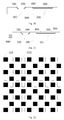
- the plurality of alternating first and second grooves 101 and 102 formed on the transparent substrate 100 can be strip-like grooves, and preferably block-like grooves, as shown in the plan view of Fig. 22 .
- the first groove 101 indicated by the black color is formed with an antireflection layer
- the second groove 102 is formed with no antireflection layer.
Landscapes
- Physics & Mathematics (AREA)
- General Physics & Mathematics (AREA)
- Optics & Photonics (AREA)
- Engineering & Computer Science (AREA)
- Manufacturing & Machinery (AREA)
- Health & Medical Sciences (AREA)
- Ophthalmology & Optometry (AREA)
- Mechanical Engineering (AREA)
- Planar Illumination Modules (AREA)
- Illuminated Signs And Luminous Advertising (AREA)
- Liquid Crystal (AREA)
Applications Claiming Priority (2)
| Application Number | Priority Date | Filing Date | Title |
|---|---|---|---|
| CN201310117205.3A CN103197370B (zh) | 2013-04-07 | 2013-04-07 | 导光板制作方法 |
| PCT/CN2013/083851 WO2014166211A1 (fr) | 2013-04-07 | 2013-09-19 | Plaque de guidage de lumière et procédé de fabrication de celle-ci, et dispositif d'affichage comportant celle-ci |
Publications (3)
| Publication Number | Publication Date |
|---|---|
| EP2985643A1 true EP2985643A1 (fr) | 2016-02-17 |
| EP2985643A4 EP2985643A4 (fr) | 2016-09-28 |
| EP2985643B1 EP2985643B1 (fr) | 2019-11-20 |
Family
ID=48720046
Family Applications (1)
| Application Number | Title | Priority Date | Filing Date |
|---|---|---|---|
| EP13861500.0A Active EP2985643B1 (fr) | 2013-04-07 | 2013-09-19 | Plaque de guidage de lumière et procédé de fabrication de celle-ci, et dispositif d'affichage comportant celle-ci |
Country Status (4)
| Country | Link |
|---|---|
| US (1) | US9651731B2 (fr) |
| EP (1) | EP2985643B1 (fr) |
| CN (1) | CN103197370B (fr) |
| WO (1) | WO2014166211A1 (fr) |
Cited By (1)
| Publication number | Priority date | Publication date | Assignee | Title |
|---|---|---|---|---|
| CN105242335A (zh) * | 2015-10-26 | 2016-01-13 | 江苏新广联科技股份有限公司 | Led面板灯用扩散板的制备方法 |
Families Citing this family (14)
| Publication number | Priority date | Publication date | Assignee | Title |
|---|---|---|---|---|
| CN103197370B (zh) * | 2013-04-07 | 2015-05-13 | 京东方科技集团股份有限公司 | 导光板制作方法 |
| KR101511117B1 (ko) * | 2014-01-07 | 2015-04-10 | 주식회사 토비스 | 양면 디스플레이장치 |
| TWI554726B (zh) * | 2014-06-27 | 2016-10-21 | 高雄晶傑達光電科技股份有限公司 | 導光板及其製造方法 |
| CN105116484A (zh) | 2015-09-15 | 2015-12-02 | 北京京东方茶谷电子有限公司 | 一种导光板、背光模组及显示装置 |
| US10088412B2 (en) * | 2016-09-27 | 2018-10-02 | Electronics & Telecommunications Research Institute | Apparatus for analyzing bio-material |
| CN110456443B (zh) * | 2019-06-25 | 2020-07-28 | 盐城华旭光电技术有限公司 | 一种背光源导光板生产用印刷蚀刻一体机 |
| JP6924958B1 (ja) * | 2020-01-31 | 2021-08-25 | 日亜化学工業株式会社 | 面状光源 |
| WO2021153561A1 (fr) * | 2020-01-31 | 2021-08-05 | 日亜化学工業株式会社 | Source de lumière plane |
| CN114355672A (zh) * | 2022-01-10 | 2022-04-15 | Tcl华星光电技术有限公司 | 光源模组、液晶显示装置以及显示设备 |
| CN114355671A (zh) | 2022-01-10 | 2022-04-15 | Tcl华星光电技术有限公司 | 光源模组、液晶显示装置以及显示设备 |
| CN114355670A (zh) * | 2022-01-10 | 2022-04-15 | Tcl华星光电技术有限公司 | 光源模组、液晶显示装置以及显示设备 |
| CN119620463B (zh) * | 2023-09-12 | 2026-02-10 | 京东方科技集团股份有限公司 | 一种背光模组及显示装置 |
| CN118409455A (zh) * | 2024-04-02 | 2024-07-30 | 昆山龙腾光电股份有限公司 | 阵列基板及显示装置 |
| CN118330960A (zh) * | 2024-04-29 | 2024-07-12 | 惠科股份有限公司 | 双面显示电子纸和显示设备 |
Family Cites Families (17)
| Publication number | Priority date | Publication date | Assignee | Title |
|---|---|---|---|---|
| JP2001351423A (ja) * | 2000-06-07 | 2001-12-21 | Minebea Co Ltd | 面状照明装置 |
| CN1165880C (zh) * | 2002-06-24 | 2004-09-08 | 卢景贵 | 金属包封组合集成型led显示器 |
| CN2545670Y (zh) * | 2002-06-24 | 2003-04-16 | 卢景贵 | 金属包封组合集成led显示器 |
| CN1236348C (zh) * | 2002-09-10 | 2006-01-11 | 统宝光电股份有限公司 | 液晶显示器的背光模组 |
| CN1276292C (zh) * | 2002-09-25 | 2006-09-20 | 胜华科技股份有限公司 | 一种具有背光及前光功能导光板的液晶显示器 |
| CN2588408Y (zh) * | 2002-12-04 | 2003-11-26 | 姚志图 | 双面发光背光源 |
| US7015989B2 (en) * | 2003-05-12 | 2006-03-21 | Lg.Philips Lcd Co., Ltd. | Liquid crystal display device using dual light unit |
| TWI226958B (en) | 2003-09-10 | 2005-01-21 | Display Optronics Corp M | Flat display |
| JP2005165199A (ja) * | 2003-12-05 | 2005-06-23 | Alps Electric Co Ltd | プリズムシート及び照光装置及び面発光装置並びに液晶表示装置 |
| JP4254529B2 (ja) | 2003-12-25 | 2009-04-15 | カシオ計算機株式会社 | モニタ付き撮像機器 |
| JP2005301016A (ja) * | 2004-04-14 | 2005-10-27 | Yowa:Kk | 液晶表示装置バックライト用導光板 |
| KR20100000234A (ko) * | 2008-06-24 | 2010-01-06 | 삼성모바일디스플레이주식회사 | 듀얼 액정표시장치 |
| WO2010138761A1 (fr) * | 2009-05-29 | 2010-12-02 | Qualcomm Mems Technologies, Inc. | Dispositifs d'éclairage et leurs procédés de fabrication |
| JP2011065049A (ja) * | 2009-09-18 | 2011-03-31 | Sekisui Chem Co Ltd | 光学シート及びその製造方法 |
| US20120120081A1 (en) * | 2010-11-16 | 2012-05-17 | Qualcomm Mems Technologies, Inc. | Illumination device with passivation layer |
| TWI443393B (zh) * | 2011-10-14 | 2014-07-01 | Au Optronics Corp | 無片式背光模組、其導光板及其製造方法 |
| CN103197370B (zh) | 2013-04-07 | 2015-05-13 | 京东方科技集团股份有限公司 | 导光板制作方法 |
-
2013
- 2013-04-07 CN CN201310117205.3A patent/CN103197370B/zh not_active Expired - Fee Related
- 2013-09-19 EP EP13861500.0A patent/EP2985643B1/fr active Active
- 2013-09-19 WO PCT/CN2013/083851 patent/WO2014166211A1/fr not_active Ceased
- 2013-09-19 US US14/364,843 patent/US9651731B2/en not_active Expired - Fee Related
Cited By (2)
| Publication number | Priority date | Publication date | Assignee | Title |
|---|---|---|---|---|
| CN105242335A (zh) * | 2015-10-26 | 2016-01-13 | 江苏新广联科技股份有限公司 | Led面板灯用扩散板的制备方法 |
| CN105242335B (zh) * | 2015-10-26 | 2017-07-04 | 江苏新广联科技股份有限公司 | Led面板灯用扩散板的制备方法 |
Also Published As
| Publication number | Publication date |
|---|---|
| EP2985643B1 (fr) | 2019-11-20 |
| WO2014166211A1 (fr) | 2014-10-16 |
| CN103197370B (zh) | 2015-05-13 |
| EP2985643A4 (fr) | 2016-09-28 |
| US9651731B2 (en) | 2017-05-16 |
| US20150309244A1 (en) | 2015-10-29 |
| CN103197370A (zh) | 2013-07-10 |
Similar Documents
| Publication | Publication Date | Title |
|---|---|---|
| EP2985643B1 (fr) | Plaque de guidage de lumière et procédé de fabrication de celle-ci, et dispositif d'affichage comportant celle-ci | |
| JP4151717B2 (ja) | 光源モジュール、光源装置及び液晶表示装置 | |
| US20220320368A1 (en) | Mini-light emitting diode light board, backlight module, and preparation method thereof | |
| EP2071391B1 (fr) | Panneau d'affichage à cristaux liquides avec matrice de microlentilles, son procédé de fabrication et dispositif d'affichage à cristaux liquides | |
| US9709864B2 (en) | Array substrate and its manufacturing method and display device | |
| KR100506088B1 (ko) | 액정표시장치 | |
| JP4458965B2 (ja) | カラーフィルター基板及びこれを有する液晶表示装置 | |
| CN113093434A (zh) | 一种显示装置 | |
| US9250466B2 (en) | Transreflective color filter and method for manufacturing the same and liquid crystal display device | |
| US20190064601A1 (en) | Transparent display panel and transparent display apparatus | |
| CN106896583B (zh) | 显示基板及其制作方法、显示面板及显示装置 | |
| EP2985642B1 (fr) | Plaque de guide lumineux et procédé de fabrication associé, source de rétroéclairage la comprenant, et dispositif d'affichage | |
| JP2009031538A (ja) | 光学素子、液晶装置、液晶装置用マザー基板、および電子機器 | |
| US20240154074A1 (en) | Display panel, method for fabricating display panel and displaying device | |
| KR20110066481A (ko) | 액정표시장치 | |
| US12197079B2 (en) | Backlight board, manufacturing method and display panel | |
| KR101818469B1 (ko) | 차광 테이프 구조 및 액정 표시 장치의 제조 방법 | |
| TWI855599B (zh) | 光源模組及反射式顯示裝置 | |
| US11327215B2 (en) | Collimating backlight module, preparation method thereof and display device | |
| US10459239B2 (en) | Naked-eye stereoscopic display grating, manufacturing method and display device | |
| WO2010035552A1 (fr) | Dispositif d'affichage à cristaux liquides et son procédé de fabrication | |
| KR100875186B1 (ko) | 표시장치 | |
| KR100916021B1 (ko) | 반투과형 액정표시장치의 어레이 기판 제조방법 | |
| CN118671875A (zh) | 光源模块及反射式显示装置 | |
| CN120019739A (zh) | 发光基板及其制备方法、背光模组、显示装置 |
Legal Events
| Date | Code | Title | Description |
|---|---|---|---|
| PUAI | Public reference made under article 153(3) epc to a published international application that has entered the european phase |
Free format text: ORIGINAL CODE: 0009012 |
|
| 17P | Request for examination filed |
Effective date: 20140616 |
|
| AK | Designated contracting states |
Kind code of ref document: A1 Designated state(s): AL AT BE BG CH CY CZ DE DK EE ES FI FR GB GR HR HU IE IS IT LI LT LU LV MC MK MT NL NO PL PT RO RS SE SI SK SM TR |
|
| AX | Request for extension of the european patent |
Extension state: BA ME |
|
| DAX | Request for extension of the european patent (deleted) | ||
| A4 | Supplementary search report drawn up and despatched |
Effective date: 20160825 |
|
| RIC1 | Information provided on ipc code assigned before grant |
Ipc: F21V 8/00 20060101ALI20160819BHEP Ipc: G03F 7/00 20060101ALI20160819BHEP Ipc: G02F 1/1333 20060101ALI20160819BHEP Ipc: G02B 1/11 20150101ALI20160819BHEP Ipc: B29D 11/00 20060101ALI20160819BHEP Ipc: G02B 6/00 20060101AFI20160819BHEP |
|
| STAA | Information on the status of an ep patent application or granted ep patent |
Free format text: STATUS: EXAMINATION IS IN PROGRESS |
|
| 17Q | First examination report despatched |
Effective date: 20170714 |
|
| GRAP | Despatch of communication of intention to grant a patent |
Free format text: ORIGINAL CODE: EPIDOSNIGR1 |
|
| STAA | Information on the status of an ep patent application or granted ep patent |
Free format text: STATUS: GRANT OF PATENT IS INTENDED |
|
| INTG | Intention to grant announced |
Effective date: 20190606 |
|
| GRAS | Grant fee paid |
Free format text: ORIGINAL CODE: EPIDOSNIGR3 |
|
| GRAA | (expected) grant |
Free format text: ORIGINAL CODE: 0009210 |
|
| STAA | Information on the status of an ep patent application or granted ep patent |
Free format text: STATUS: THE PATENT HAS BEEN GRANTED |
|
| AK | Designated contracting states |
Kind code of ref document: B1 Designated state(s): AL AT BE BG CH CY CZ DE DK EE ES FI FR GB GR HR HU IE IS IT LI LT LU LV MC MK MT NL NO PL PT RO RS SE SI SK SM TR |
|
| REG | Reference to a national code |
Ref country code: GB Ref legal event code: FG4D |
|
| REG | Reference to a national code |
Ref country code: CH Ref legal event code: EP |
|
| REG | Reference to a national code |
Ref country code: IE Ref legal event code: FG4D |
|
| REG | Reference to a national code |
Ref country code: DE Ref legal event code: R096 Ref document number: 602013063225 Country of ref document: DE |
|
| REG | Reference to a national code |
Ref country code: AT Ref legal event code: REF Ref document number: 1204814 Country of ref document: AT Kind code of ref document: T Effective date: 20191215 |
|
| REG | Reference to a national code |
Ref country code: NL Ref legal event code: MP Effective date: 20191120 |
|
| REG | Reference to a national code |
Ref country code: LT Ref legal event code: MG4D |
|
| PG25 | Lapsed in a contracting state [announced via postgrant information from national office to epo] |
Ref country code: SE Free format text: LAPSE BECAUSE OF FAILURE TO SUBMIT A TRANSLATION OF THE DESCRIPTION OR TO PAY THE FEE WITHIN THE PRESCRIBED TIME-LIMIT Effective date: 20191120 Ref country code: LV Free format text: LAPSE BECAUSE OF FAILURE TO SUBMIT A TRANSLATION OF THE DESCRIPTION OR TO PAY THE FEE WITHIN THE PRESCRIBED TIME-LIMIT Effective date: 20191120 Ref country code: GR Free format text: LAPSE BECAUSE OF FAILURE TO SUBMIT A TRANSLATION OF THE DESCRIPTION OR TO PAY THE FEE WITHIN THE PRESCRIBED TIME-LIMIT Effective date: 20200221 Ref country code: NO Free format text: LAPSE BECAUSE OF FAILURE TO SUBMIT A TRANSLATION OF THE DESCRIPTION OR TO PAY THE FEE WITHIN THE PRESCRIBED TIME-LIMIT Effective date: 20200220 Ref country code: LT Free format text: LAPSE BECAUSE OF FAILURE TO SUBMIT A TRANSLATION OF THE DESCRIPTION OR TO PAY THE FEE WITHIN THE PRESCRIBED TIME-LIMIT Effective date: 20191120 Ref country code: NL Free format text: LAPSE BECAUSE OF FAILURE TO SUBMIT A TRANSLATION OF THE DESCRIPTION OR TO PAY THE FEE WITHIN THE PRESCRIBED TIME-LIMIT Effective date: 20191120 Ref country code: BG Free format text: LAPSE BECAUSE OF FAILURE TO SUBMIT A TRANSLATION OF THE DESCRIPTION OR TO PAY THE FEE WITHIN THE PRESCRIBED TIME-LIMIT Effective date: 20200220 Ref country code: FI Free format text: LAPSE BECAUSE OF FAILURE TO SUBMIT A TRANSLATION OF THE DESCRIPTION OR TO PAY THE FEE WITHIN THE PRESCRIBED TIME-LIMIT Effective date: 20191120 |
|
| PG25 | Lapsed in a contracting state [announced via postgrant information from national office to epo] |
Ref country code: RS Free format text: LAPSE BECAUSE OF FAILURE TO SUBMIT A TRANSLATION OF THE DESCRIPTION OR TO PAY THE FEE WITHIN THE PRESCRIBED TIME-LIMIT Effective date: 20191120 Ref country code: HR Free format text: LAPSE BECAUSE OF FAILURE TO SUBMIT A TRANSLATION OF THE DESCRIPTION OR TO PAY THE FEE WITHIN THE PRESCRIBED TIME-LIMIT Effective date: 20191120 Ref country code: IS Free format text: LAPSE BECAUSE OF FAILURE TO SUBMIT A TRANSLATION OF THE DESCRIPTION OR TO PAY THE FEE WITHIN THE PRESCRIBED TIME-LIMIT Effective date: 20200320 |
|
| PG25 | Lapsed in a contracting state [announced via postgrant information from national office to epo] |
Ref country code: AL Free format text: LAPSE BECAUSE OF FAILURE TO SUBMIT A TRANSLATION OF THE DESCRIPTION OR TO PAY THE FEE WITHIN THE PRESCRIBED TIME-LIMIT Effective date: 20191120 |
|
| PG25 | Lapsed in a contracting state [announced via postgrant information from national office to epo] |
Ref country code: PT Free format text: LAPSE BECAUSE OF FAILURE TO SUBMIT A TRANSLATION OF THE DESCRIPTION OR TO PAY THE FEE WITHIN THE PRESCRIBED TIME-LIMIT Effective date: 20200412 Ref country code: EE Free format text: LAPSE BECAUSE OF FAILURE TO SUBMIT A TRANSLATION OF THE DESCRIPTION OR TO PAY THE FEE WITHIN THE PRESCRIBED TIME-LIMIT Effective date: 20191120 Ref country code: DK Free format text: LAPSE BECAUSE OF FAILURE TO SUBMIT A TRANSLATION OF THE DESCRIPTION OR TO PAY THE FEE WITHIN THE PRESCRIBED TIME-LIMIT Effective date: 20191120 Ref country code: CZ Free format text: LAPSE BECAUSE OF FAILURE TO SUBMIT A TRANSLATION OF THE DESCRIPTION OR TO PAY THE FEE WITHIN THE PRESCRIBED TIME-LIMIT Effective date: 20191120 Ref country code: RO Free format text: LAPSE BECAUSE OF FAILURE TO SUBMIT A TRANSLATION OF THE DESCRIPTION OR TO PAY THE FEE WITHIN THE PRESCRIBED TIME-LIMIT Effective date: 20191120 Ref country code: ES Free format text: LAPSE BECAUSE OF FAILURE TO SUBMIT A TRANSLATION OF THE DESCRIPTION OR TO PAY THE FEE WITHIN THE PRESCRIBED TIME-LIMIT Effective date: 20191120 |
|
| REG | Reference to a national code |
Ref country code: AT Ref legal event code: MK05 Ref document number: 1204814 Country of ref document: AT Kind code of ref document: T Effective date: 20191120 |
|
| REG | Reference to a national code |
Ref country code: DE Ref legal event code: R097 Ref document number: 602013063225 Country of ref document: DE |
|
| PG25 | Lapsed in a contracting state [announced via postgrant information from national office to epo] |
Ref country code: SM Free format text: LAPSE BECAUSE OF FAILURE TO SUBMIT A TRANSLATION OF THE DESCRIPTION OR TO PAY THE FEE WITHIN THE PRESCRIBED TIME-LIMIT Effective date: 20191120 Ref country code: SK Free format text: LAPSE BECAUSE OF FAILURE TO SUBMIT A TRANSLATION OF THE DESCRIPTION OR TO PAY THE FEE WITHIN THE PRESCRIBED TIME-LIMIT Effective date: 20191120 |
|
| PLBE | No opposition filed within time limit |
Free format text: ORIGINAL CODE: 0009261 |
|
| STAA | Information on the status of an ep patent application or granted ep patent |
Free format text: STATUS: NO OPPOSITION FILED WITHIN TIME LIMIT |
|
| 26N | No opposition filed |
Effective date: 20200821 |
|
| PGFP | Annual fee paid to national office [announced via postgrant information from national office to epo] |
Ref country code: DE Payment date: 20200925 Year of fee payment: 8 |
|
| PG25 | Lapsed in a contracting state [announced via postgrant information from national office to epo] |
Ref country code: AT Free format text: LAPSE BECAUSE OF FAILURE TO SUBMIT A TRANSLATION OF THE DESCRIPTION OR TO PAY THE FEE WITHIN THE PRESCRIBED TIME-LIMIT Effective date: 20191120 Ref country code: PL Free format text: LAPSE BECAUSE OF FAILURE TO SUBMIT A TRANSLATION OF THE DESCRIPTION OR TO PAY THE FEE WITHIN THE PRESCRIBED TIME-LIMIT Effective date: 20191120 Ref country code: SI Free format text: LAPSE BECAUSE OF FAILURE TO SUBMIT A TRANSLATION OF THE DESCRIPTION OR TO PAY THE FEE WITHIN THE PRESCRIBED TIME-LIMIT Effective date: 20191120 |
|
| PG25 | Lapsed in a contracting state [announced via postgrant information from national office to epo] |
Ref country code: IT Free format text: LAPSE BECAUSE OF FAILURE TO SUBMIT A TRANSLATION OF THE DESCRIPTION OR TO PAY THE FEE WITHIN THE PRESCRIBED TIME-LIMIT Effective date: 20191120 |
|
| PG25 | Lapsed in a contracting state [announced via postgrant information from national office to epo] |
Ref country code: MC Free format text: LAPSE BECAUSE OF FAILURE TO SUBMIT A TRANSLATION OF THE DESCRIPTION OR TO PAY THE FEE WITHIN THE PRESCRIBED TIME-LIMIT Effective date: 20191120 |
|
| REG | Reference to a national code |
Ref country code: CH Ref legal event code: PL |
|
| GBPC | Gb: european patent ceased through non-payment of renewal fee |
Effective date: 20200919 |
|
| REG | Reference to a national code |
Ref country code: BE Ref legal event code: MM Effective date: 20200930 |
|
| PG25 | Lapsed in a contracting state [announced via postgrant information from national office to epo] |
Ref country code: LU Free format text: LAPSE BECAUSE OF NON-PAYMENT OF DUE FEES Effective date: 20200919 |
|
| PG25 | Lapsed in a contracting state [announced via postgrant information from national office to epo] |
Ref country code: FR Free format text: LAPSE BECAUSE OF NON-PAYMENT OF DUE FEES Effective date: 20200930 |
|
| PG25 | Lapsed in a contracting state [announced via postgrant information from national office to epo] |
Ref country code: LI Free format text: LAPSE BECAUSE OF NON-PAYMENT OF DUE FEES Effective date: 20200930 Ref country code: GB Free format text: LAPSE BECAUSE OF NON-PAYMENT OF DUE FEES Effective date: 20200919 Ref country code: IE Free format text: LAPSE BECAUSE OF NON-PAYMENT OF DUE FEES Effective date: 20200919 Ref country code: BE Free format text: LAPSE BECAUSE OF NON-PAYMENT OF DUE FEES Effective date: 20200930 Ref country code: CH Free format text: LAPSE BECAUSE OF NON-PAYMENT OF DUE FEES Effective date: 20200930 |
|
| REG | Reference to a national code |
Ref country code: DE Ref legal event code: R119 Ref document number: 602013063225 Country of ref document: DE |
|
| PG25 | Lapsed in a contracting state [announced via postgrant information from national office to epo] |
Ref country code: TR Free format text: LAPSE BECAUSE OF FAILURE TO SUBMIT A TRANSLATION OF THE DESCRIPTION OR TO PAY THE FEE WITHIN THE PRESCRIBED TIME-LIMIT Effective date: 20191120 Ref country code: MT Free format text: LAPSE BECAUSE OF FAILURE TO SUBMIT A TRANSLATION OF THE DESCRIPTION OR TO PAY THE FEE WITHIN THE PRESCRIBED TIME-LIMIT Effective date: 20191120 Ref country code: CY Free format text: LAPSE BECAUSE OF FAILURE TO SUBMIT A TRANSLATION OF THE DESCRIPTION OR TO PAY THE FEE WITHIN THE PRESCRIBED TIME-LIMIT Effective date: 20191120 |
|
| PG25 | Lapsed in a contracting state [announced via postgrant information from national office to epo] |
Ref country code: MK Free format text: LAPSE BECAUSE OF FAILURE TO SUBMIT A TRANSLATION OF THE DESCRIPTION OR TO PAY THE FEE WITHIN THE PRESCRIBED TIME-LIMIT Effective date: 20191120 |
|
| PG25 | Lapsed in a contracting state [announced via postgrant information from national office to epo] |
Ref country code: DE Free format text: LAPSE BECAUSE OF NON-PAYMENT OF DUE FEES Effective date: 20220401 |