EP2987086B1 - Informatique sécurisée - Google Patents
Informatique sécurisée Download PDFInfo
- Publication number
- EP2987086B1 EP2987086B1 EP14784683.6A EP14784683A EP2987086B1 EP 2987086 B1 EP2987086 B1 EP 2987086B1 EP 14784683 A EP14784683 A EP 14784683A EP 2987086 B1 EP2987086 B1 EP 2987086B1
- Authority
- EP
- European Patent Office
- Prior art keywords
- data
- lfsr
- cache
- instruction
- code
- Prior art date
- Legal status (The legal status is an assumption and is not a legal conclusion. Google has not performed a legal analysis and makes no representation as to the accuracy of the status listed.)
- Active
Links
Images


Classifications
-
- G—PHYSICS
- G06—COMPUTING OR CALCULATING; COUNTING
- G06F—ELECTRIC DIGITAL DATA PROCESSING
- G06F12/00—Accessing, addressing or allocating within memory systems or architectures
- G06F12/14—Protection against unauthorised use of memory or access to memory
- G06F12/1408—Protection against unauthorised use of memory or access to memory by using cryptography
-
- G—PHYSICS
- G06—COMPUTING OR CALCULATING; COUNTING
- G06F—ELECTRIC DIGITAL DATA PROCESSING
- G06F12/00—Accessing, addressing or allocating within memory systems or architectures
- G06F12/02—Addressing or allocation; Relocation
- G06F12/08—Addressing or allocation; Relocation in hierarchically structured memory systems, e.g. virtual memory systems
- G06F12/0802—Addressing of a memory level in which the access to the desired data or data block requires associative addressing means, e.g. caches
- G06F12/0875—Addressing of a memory level in which the access to the desired data or data block requires associative addressing means, e.g. caches with dedicated cache, e.g. instruction or stack
-
- G—PHYSICS
- G06—COMPUTING OR CALCULATING; COUNTING
- G06F—ELECTRIC DIGITAL DATA PROCESSING
- G06F21/00—Security arrangements for protecting computers, components thereof, programs or data against unauthorised activity
- G06F21/50—Monitoring users, programs or devices to maintain the integrity of platforms, e.g. of processors, firmware or operating systems
- G06F21/52—Monitoring users, programs or devices to maintain the integrity of platforms, e.g. of processors, firmware or operating systems during program execution, e.g. stack integrity ; Preventing unwanted data erasure; Buffer overflow
-
- G—PHYSICS
- G06—COMPUTING OR CALCULATING; COUNTING
- G06F—ELECTRIC DIGITAL DATA PROCESSING
- G06F21/00—Security arrangements for protecting computers, components thereof, programs or data against unauthorised activity
- G06F21/70—Protecting specific internal or peripheral components, in which the protection of a component leads to protection of the entire computer
- G06F21/82—Protecting input, output or interconnection devices
- G06F21/85—Protecting input, output or interconnection devices interconnection devices, e.g. bus-connected or in-line devices
-
- G—PHYSICS
- G06—COMPUTING OR CALCULATING; COUNTING
- G06F—ELECTRIC DIGITAL DATA PROCESSING
- G06F9/00—Arrangements for program control, e.g. control units
- G06F9/06—Arrangements for program control, e.g. control units using stored programs, i.e. using an internal store of processing equipment to receive or retain programs
- G06F9/30—Arrangements for executing machine instructions, e.g. instruction decode
- G06F9/3017—Runtime instruction translation, e.g. macros
- G06F9/30178—Runtime instruction translation, e.g. macros of compressed or encrypted instructions
-
- G—PHYSICS
- G06—COMPUTING OR CALCULATING; COUNTING
- G06F—ELECTRIC DIGITAL DATA PROCESSING
- G06F2212/00—Indexing scheme relating to accessing, addressing or allocation within memory systems or architectures
- G06F2212/40—Specific encoding of data in memory or cache
- G06F2212/402—Encrypted data
-
- G—PHYSICS
- G06—COMPUTING OR CALCULATING; COUNTING
- G06F—ELECTRIC DIGITAL DATA PROCESSING
- G06F2212/00—Indexing scheme relating to accessing, addressing or allocation within memory systems or architectures
- G06F2212/45—Caching of specific data in cache memory
- G06F2212/452—Instruction code
-
- G—PHYSICS
- G06—COMPUTING OR CALCULATING; COUNTING
- G06F—ELECTRIC DIGITAL DATA PROCESSING
- G06F2221/00—Indexing scheme relating to security arrangements for protecting computers, components thereof, programs or data against unauthorised activity
- G06F2221/21—Indexing scheme relating to G06F21/00 and subgroups addressing additional information or applications relating to security arrangements for protecting computers, components thereof, programs or data against unauthorised activity
- G06F2221/2125—Just-in-time application of countermeasures, e.g., on-the-fly decryption, just-in-time obfuscation or de-obfuscation
Definitions
- Embodiments of the present invention may relate to processing encrypted code and data in a secure manner in a processor.
- Convolution encrypting the source code while helpful, may still be decrypted by detecting the frequency of the instruction codes.
- Other techniques such as decrypting the instruction by applying the XOR of the encrypted instruction and one or more fixed keys such as described by Henry et al., in US Patent Application Publication No. 2011/0296204, published December 1, 2011 , are only as good as the keys.
- a sufficiently robust encryption technique may be needed to be adequately tamper proof. Such a technique should be sufficiently random to be difficult to break. Butler, in US Patent No.
- MISR Multiple Input Shift Register
- LFSR linear feedback shift register
- BIST built-in self test
- RSA Rivest-Shamir-Adelman
- Butler's encryption approach may require too much computational overhead for encoding and decoding a processor's instructions and data, as may other software-based encryption techniques, such as that described by Horovitz et al. in US Patent Application Publication No. 2013/0067245, published March 14,2013 ; and while Henry et al., in US Patent Application Publication No.
- Various embodiments of the invention may relate to hardware and software encryption and decryption techniques using pseudo-random numbers generated by LFSRs for use in both testing a processor's hardware and protecting a processor's data and instructions in shared memory by encrypting and decrypting the data and instructions between the processor and all shared memory.
- WO 2011/149986 discloses a single processor system with techniques for memory compartmentalization for trusted execution of a virtual machine in this architecture.
- the single processor system comprise a processing core having an instruction cache and a data cache, and the ability to process instructions and operate on data.
- An encrypt/decrypt block is located between the L2 cache and L3 cache and memory compartmentalization may be achieved by encrypting L3 cache lines using a key under the control of a given virtual machine within the trust boundaries of the processing core on which that virtual machine is executed.
- a multi-processor system having two or more processors, each processor including:
- the LFSR includes a programmable LFSR.
- the logic configured to translate data includes logic configured to selectively encrypt data written to the system bus.
- an integrated circuit including the multi-processor system herein above defined.
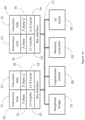
- FIG. 1a a conceptual diagram of an example of a multi-processor system with encryption and decryption.
- the system may include two processors 10 connected via a common system bus 17 to a shared L2 cache 18 and/or other devices, such as a memory controller 19, one or more co-processor(s) 20, and/or a bridge to more peripheral devices 21.
- Each processor 10 may include an instruction unit 11 and its corresponding L,1 I-cache 13 with a translator 15 for decrypting the instructions being read into the I-cache coupled between them.
- each processor 10 may contain an execution unit 12 and its corresponding L1 D-cache 14 with another translator 16 for encrypting and decrypting data being read into and written out of the D-cache coupled between them.
- the instructions and data may be decrypted as they are read out of their respective L1 caches, and selected decrypted data may be sent past the L1 D-cache 14 to the bridge 21 and co-processors 20, while maintaining the encrypted data in the cache.
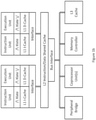
- the architecture shown in Figure la may have processors with reduced instruction set computing (RISC) and instructions that use base register plus index addressing, but it is further contemplated that LFSR encryption and decryption of individual processor instructions and data may be employed in other processor architectures, such as complex instruction set computing (CISC) with direct addressing modes, and a system architecture, including but not limited to the one shown in Figure 1b .
- RISC reduced instruction set computing
- CISC complex instruction set computing
- system architecture including but not limited to the one shown in Figure 1b .
- Figure 2a a diagram of an example of instruction decryption using an LFSR in conjunction with an instruction address register.
- an instruction LFSR 23 containing a code that may be used to decrypt the encoded instructions 24 using a set of exclusive-OR gates 25.
- the instruction LFSR 23 may be clocked each time the instruction address register 22 is incremented, thereby providing each instruction with a unique code from which the instruction may be decoded. In this manner, each occurrence of an instruction may be encoded and decoded differently, thereby obscuring the actual instruction's identity.
- the normal instructions may consist of opcode 26 and address 27 fields.
- the address fields may contain offsets from base register addresses for accessing data.
- selected instructions may also include translation codes 28.
- the fields and translation codes may initially be encrypted and may be decrypted before being used.
- One such selected instruction, the branch instruction may load both the instruction address register and the instruction LFSR while executing the branch, such that the instruction LFSR may contain the proper code for the next instruction 29 after taking the branch.
- the instruction address register may be incremented, and the LFSR may be clocked to provide the proper code for decrypting the next instruction.
- Subsequent incrementing of the instruction address register and clocking of the LFSR may occur until the instruction 29 may be reached, at which point the contents of the LFSR may match the decrypted translation code 28 of the corresponding branch instruction.
- An initial translation code for the first instruction 30, and other data may be obtained by the operating system through some separate secure encryption protocol, such as RSA, which may be loaded into the instruction LFSR using a branch to the first instruction.
- some encrypted instructions may include translation codes, which may also be encrypted, thereby securing all but the initial translation code for the first instruction. In this manner, the proper translation code for each instruction may be easily obtained in one clock cycle by either loading or clocking the LFSR.
- Each processor may contain a set of N registers 30, where the first K registers may be used to hold data, and the last N-K base registers may contain addresses pointing to one or more sections of data and/or instruction code.
- the processor may further contain N-K translation code registers 31, which may correspond to the N-K base registers.
- an executed instruction When an executed instruction loads or stores data from or to a memory location, it may calculate the address of the memory location by adding an offset to the address within a base register.
- the translation code corresponding to that address may be calculated by transforming the code from the translation code associated with the base register by the amount of the offset, thereby creating a code for decrypting or encrypting the corresponding data.
- the translation code for a location 37 with an offset 35 from the address in base register K may be calculated by loading the offset 35 and the translation code from code register K 33 into the code transformation logic 34, producing a translation code in register 36 for the location 37, which, when applied to the exclusive-ORs 38 in Figure 3c , may decrypt or encrypt the data 39 being loaded from or stored into location 37.
- the same translation code may be used to encrypt and decrypt data being put into or taken from the target address.
- the same translation code result as obtained through the code transformation logic 34 may be obtained by loading a properly wired LFSR with the translation code from code register K and clocking the LFSR by a count equal to the offset 35.
- multiplexors 40 may be used to select the unencrypted data 39 when sending the data to either the co-processors 20 in Figure la or other peripheral devices through the peripheral bridge 21 in Figure 1a , or to other locations that may require decrypted data.
- the multiplexors 40 in Figure 3c may continue to select the encrypted data when sending the data either back to the caches 14 and 18 in Figure la or to main memory through the memory controller 19 in Figure 1a . Such selection may be done by a select line 41 in Figure 3c , which may be driven either from a control register (not shown) or by control bits within the instructions themselves.
- instructions for loading a base register's address may also load the base register's associated code register.
- a subroutine call may store the translation code associated with the instruction in the instruction LFSR after saving the prior contents of the LFSR in the code register associated with the base register where it stores its return address.
- a return instruction may branch to the address in the base register while loading the contents of the corresponding code register into the instruction LFSR.
- Initial encryption of the instructions in a program and data space may be performed after compilation and before the final load module creation, e.g., by: creating an initial translation code; incrementing the LFSR function to obtain the translation code for each instruction; defining a translation code for each data space; incrementing the LFSR function to obtain the translation code for each predefined data element; appending to selected instructions the translation code corresponding to the value in the address field of those instructions; and encoding each instruction, data and appended translation code with the translation code associated with its address.
- the instructions requiring appended translation codes may include instructions involving addresses in base registers, branches and/or subroutine calls.
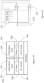
- FIG 4 a simplified diagram of an example of a L1 data cache.
- the L1 Cache 45 may be coupled to both a write line buffer 43 and a read line buffer 44.
- the contents of the data cache may be encrypted in a manner similar to the system architecture shown in Figure 1a
- the read line buffer 42 may be coupled to the data inputs 39 in Figure 3c for decryption of the encrypted data.
- the write line buffer 43 may also be connected to the outputs 42 in Figure 3c for re-encryption of updated data and may be configured to read the register 36, to load the associated translation code into a portion of the data cache 46 along with the encrypted updated data.
- Part of the write line buffer 43 may also be connected to read the output register 36 following execution of the code transformation logic 34.
- the translation code associated with the new cache line data may be generated while the data portion of the write line buffer 43 may be filled from external cache or memory.
- the translation code may be read from a section of the cache 46 into the register 36 to subsequently translate the read line buffer's 44 data for the execution unit.
- other devices snoop the L1 Cache, they may only extract encrypted data.
- the contents of the L1 cache may be decrypted in the system architecture depicted in Figure 1a .
- the processor may not decrypt the data or instructions from the cache. Rather the translation code 36 for the address of the data or instructions being written into the write line buffer may be used to decrypt the data or instructions and may be subsequently stored in a code portion 46 of the cache along with the decrypted data.
- the translation code associated with the data may be used to encrypt the snooped data.
- an LFSR starting with a translation code for the first instruction or word of data in a cache line buffer, may be clocked and applied to each subsequent instruction or word of data being read from or written into the cache line buffer. If the read or write is out of order, the translation code may be adjusted by a single transformation function that may "subtract" the buffer size from the LFSR when the data or instructions wrap around the line buffer. Given an LFSR function with M unique values before repeating, "subtraction" of N is equivalent to a transformation function of M-N, where M>N.
- FIG. 5 a diagram of an example four-bit Galois LFSR composed of four flip-flops 51-54 serially coupled in a ring, with one exclusive-OR gate 55 connected between the first flip-flop 51 and the second flip-flop 52, and a feedback loop 56 connecting the fourth flip-flop 54 to the exclusive-OR 55 and the first flip-flop 51, where the outputs of all the flip-flops are coupled to a code register 57.
- This particular LFSR may be used to generate all fifteen distinct non-zero translation codes (i.e., all fifteen distinct non-zero combinations of four bits) before repeating.
- FIG. 6a a high level diagram of an example of offset translation based on the example LFSR of Figure 5 .
- M clocks may be used to generate the translation code for an address of the Mth word after the specific address.
- the initial translation code C 0 60 may applied with an offset value 61 to code transformation logic 63 to produce a translation code C M in an output code register 62, which corresponds to the translation code the Mth word after the specific address.
- the code transformation logic may produce translation code C M by successively, for each set (i.e., "1” or “high”), or alternatively, clear (i.e., "0” or “low”) bit in an Nth position of the binary offset value, transforming the initial translation code by a function that is equivalent to clocking the LFSR by 2 N times.
- the code transformation logic may transform the translation code by some combination of the transformation functions: JI (one clock) 64, J2 (two clocks) 65, J4 (four clocks) 66 and/or J8 (8 clocks) 67.
- Each of the functions J1 through J8 may be comprised of exclusive-OR gates 69 and multiplexors 68.
- the function J1 64 may select the four bits from C 0 60 if the lowest order bit from the offset 61 is low, and may select the same values the LFSR would generate in one clock cycle if the lowest order bit from the offset 61 is high.
- the second bit is the exclusive-OR 69 of the first and fourth bits, as would be captured in the second flip-flop 51 of the LFSR in Figure 5 after one clock.
- the function J2 65 may select between its input values if bit1 of the offset is low and the same values the LFSR would generate after two clock cycles, which is equivalent to two cycles of J1, if bit1 of the offset is high. In this manner, each respective bit of the offset selects a corresponding function equivalent to clocking the LFSR by the number of clock cycles corresponding to the position of the offset bit, depending on whether the respective offset bit is high or low.
- FIG. 7 a diagram of a code transformation logic example with a six-bit offset.
- the same type of modulo calculation may be applied to generate code transformation logic for any LFSR with any size offset.
- the LFSR 80 may contain any number of flip-flops 81 serially coupled in a ring, where each flip-flop, except the last flip-flop 82, may drive an exclusive-OR gate 83, and all may be driven by a multiplexor 84, which may select between loading a code 85 into the LFSR or sequencing the LFSR.
- Each exclusive-OR gate 83 may also be driven by an AND gate 86, which may be used to enable the signal on the feedback line 87 with a bit from an LFSR mask register 88.
- the LFSR mask register 88 may contain N-1 bits for an N flip-flop LFSR.
- the LFSR mask register bits may be loaded with any Galois LFSR configuration.
- the LFSR may be clocked on all increments of the instruction address register, thereby stepping through the LFSR states. In any one of the ideal configurations, the LFSR may repeat every state possible except zero. Loading a zero code into the LFSR may be equivalent to no decryption, given that no amount of clock may change the state of the LFSR and that no bits are changed when exclusive-ORed with zero.
- the LFSRs and all decryption may be disabled by loading translation codes of zero. This may be performed, e.g., when exiting an encrypted application.
- Each respective transformation function 90 may include N transform mask registers 91 of N bits each, where N is the number of flip-flops in the corresponding LFSR. There may be one transform mask register for each output of the transformation function. Each of the bits in the transform mask registers may be used to select, via an AND gate 92, a corresponding input to the transformation function. The selected inputs may be exclusive-ORed, through a tree of exclusive-OR gates 93, to form the output 94 selected by a bit 95 from the offset 96.
- programmable code transformation logic for an N-bit offset may require up to N 3 programming bits. It should be noted that the transformation functions selected by all offset bits above N may be copies of the first N transformation functions, thereby requiring no additional programming bits.
- the actual number of unique bits required to program the code transformation logic may be much less than N 3 .
- the transform mask register bits for the first transformation function when viewed as an NxN matrix, may be generated by rotating an identity matrix down one row after ORing the N-1 LFSR mask register bits into the first bits of the last column, in a manner that properly simulates one clock shift of the associated LFSR.
- the second transformation function's matrix may be generated by multiplying modulo 2 the first transformation function's matrix by itself
- the third transformation function's matrix may be generated by multiplying modulo 2 the second matrix by itself
- each successive transformation function's matrix may be generated from the matrix of the previous transformation function in the same manner.
- the N 3 programming bits of a programmable code transformation function may be generated with as few as N ⁇ 1 programmable bits, or may, with appropriate logic, only require N ⁇ 1 programmable bits.
- the LFSR mask register bits needed for programming the LFSR may not be the bits used to program the transformation functions, thereby providing different encryption algorithms for the instruction and data. Such additional mask register bits may also be included with the initial translation code.
- the mask register bits may be encrypted with the initial translation code, and prior to executing the encrypted program, the mask register data may be decrypted by loading the initial translation code into the LFSR, using the initial translation code to decode the mask register data without clocking the LFSR, and then loading the LFSR's decrypted mask register data.
- instructions to generate the data for the transform mask registers from the LFSR's mask register bits may be encrypted, appended in front of the encoded application, and may be executed following the loading of the LFSR mask register and initial translation code. It should be noted that this code may not address data memory, which may require the use of the yet-to-be-programmed code transformation logic. As such, all transform mask registers may be directly addressable by instructions, and all generation of the transform mask register data may be done in situ, thereby avoiding use of addressed data memory.
- the processor's legal instruction codes may be a small traction of the possible values in the opcode field of an instruction.
- the execution of an illegal instruction may cause an operating system interrupt, thereby allowing the operating system to detect instruction tampering.
- illegal addresses may also cause operating system interrupts, thereby allowing the operating system to detect data tampering.
- a practical example may be a 32-bit RISC processor with 20-bit offset address fields in the instructions and multiple levels of cache.
- the instructions and data may remain encrypted within their respective caches, the LFSR may be 32 bits long, and the LFSR mask register may be 31 bits long, both manageable sizes of separately encrypted initial codes.
- the longest path between flip-flops on the programmable LFSR may be an AND gate followed by XOR gate, and loading the LFSR may also only take one clock cycle: hence, the decryption of the instructions may easily occur during the instruction unit's fetch cycle.
- the proper decrypted translation codes for each stream may be stored with the branch predictions or loop instructions.
- the data code transformation logic may be much larger.
- the offset address field may contain a 20-bit offset, which may result in 20 transformation functions, each of which may have 32 bits of 32 AND gates masking the input signals to a 6-level tree of 31 XOR gates.
- Each of the 20 transformation functions may then contain eight levels of logic (1 AND, 6 XORs and 1 multiplexor), for a total of 1,024 AND gates, 992 XOR gates, 32 multiplexors, and 32 32-bit transform mask registers.
- the worst-case path in such a structure may be up to 160 gate levels long. This may be reduced where the terms are not needed, but the result may still require many clock cycles.
- the time needed to calculate the proper cache line translation code may overlap with the time required to process a cache line miss request to either an L2 cache or main memory, which also may take many clock cycles.
- the translation code may be stored in the L1 data cache with the encrypted cache line.
- the translation code may be retrieved to decrypt the data retrieved from the cache or to encrypt the data written to the cache, as shown in Figure 4 .
- the translation code stored in the cache may be only applicable to the first word in a 2 K word cache line.
- a K-bit code transformation logic block may then be used to create the translation code for the proper word out of the cache line, or a combination of a K-M bit code transformation logic block and 2 M cycles of an appropriately loaded LFSR may be used. It should be noted that, because of the short path within the LFSR, the LFSR may also be clocked at a multiple of the processor clock.
- the mask register and code transformation logic may be reduced by limiting the programming to a subset of the bits.
- debugging of applications may be performed without recompiling the application or altering its cycle-by-cycle operation.
- Unencrypted applications may also be modified before the final load module creation, e.g., by creating a zero initial translation code and appending to the selected instructions a zero translation code.
- Execution of the unencrypted application may then be performed with all the available transparent debug facilities as may exist in the processor, and with the translation logic enabled.
- the unencrypted code may then perform in the same cycle-by-cycle manner as the encrypted code.
- its size and cycle-by-cycle operation may not change.
- the LFSR, code transformation logic, and checksum logic may be used to generate random instructions and data to test the processor prior to normal operation.
- Figure 10 another diagram of an example of a processor 100 with checksum logic 107 coupled to the output of the instruction unit 101 and checksum logic 108 coupled to the output of the execution unit 102.
- the L1 caches 103 and 104 may be initialized to zero.
- Figure 11 a diagram of an example of checksum logic.
- the checksum register 111 may be cleared or loaded with an initial code.
- the input data 112 may be combined with the current contents of the checksum register 111 through exclusive-OR (XOR) gates 113 to update the checksum register 1 11.
- the input data 112 may be instructions or control signals from the instruction unit or may be data and control signals from the execution unit. Testing may proceed by:
- the control signals may include interrupt signals, instruction addresses, and/or other signals generated by the execution of the test and captured by the checksum prior to being disabled.
- some amount of encoded instructions may be loaded into the I-cache, and encoded data into the D-cache to perform partial or full diagnostic tests.
- the LFSR, transformation logic and checksums may be used to perform processor BIST or to aid in processor diagnostic tests.
Landscapes
- Engineering & Computer Science (AREA)
- Theoretical Computer Science (AREA)
- Computer Security & Cryptography (AREA)
- Physics & Mathematics (AREA)
- General Engineering & Computer Science (AREA)
- General Physics & Mathematics (AREA)
- Software Systems (AREA)
- Computer Hardware Design (AREA)
- Storage Device Security (AREA)
- Executing Machine-Instructions (AREA)
- Test And Diagnosis Of Digital Computers (AREA)
- Mathematical Physics (AREA)
Claims (4)
- Système multiprocesseur présentant deux ou plusieurs processeurs (10), chaque processeur comportant :une unité d'instruction (11) destinée à traiter les instructions ;une mémoire cache d'instruction (13) ;une unité d'exécution (12) destinée à opérer sur des données ;une mémoire cache de données (14) ;au moins une interface avec un bus système (17) ;la logique (15) entre l'unité d'instruction (11) et la mémoire cache d'instruction (13) et configurée pour traduire les instructions auxquelles l'unité d'instruction (11) accède à partir de la mémoire cache d'instruction (13) ; etla logique (16) entre l'unité d'exécution (12) et la mémoire cache de données (14) et configurée pour accéder à la mémoire cache de données (14) et pour traduire les données ;dans lequel la traduction des instructions, des données, ou des deux, utilise des nombres pseudo aléatoires ;dans lequel la logique (15) configurée pour traduire les instructions comprend un registre à décalage à rétroaction linéaire (LFSR) et une logique configurée pour déchiffrer les instructions codées ; etdans lequel la logique (16) configurée pour traduire des données comprend une logique de transformation de code configurée pour déchiffrer des données auxquelles accède l'unité d'exécution (12) et pour chiffrer des données écrites dans la mémoire cache de données (14).
- Système multiprocesseur selon la revendication 1, dans lequel le LFSR comporte un LFSR programmable.
- Système multiprocesseur selon la revendication 1, dans lequel la logique (16) configurée pour accéder à la mémoire cache de données (14) comprend une logique configurée pour chiffrer de manière sélective les données écrites sur le bus système (17).
- Circuit intégré comportant le système multiprocesseur selon la revendication 1.
Applications Claiming Priority (2)
| Application Number | Priority Date | Filing Date | Title |
|---|---|---|---|
| US13/864,688 US9280490B2 (en) | 2013-04-17 | 2013-04-17 | Secure computing |
| PCT/US2014/031396 WO2014172062A2 (fr) | 2013-04-17 | 2014-03-21 | Informatique securisee |
Publications (3)
| Publication Number | Publication Date |
|---|---|
| EP2987086A2 EP2987086A2 (fr) | 2016-02-24 |
| EP2987086A4 EP2987086A4 (fr) | 2016-12-14 |
| EP2987086B1 true EP2987086B1 (fr) | 2022-03-02 |
Family
ID=51729960
Family Applications (1)
| Application Number | Title | Priority Date | Filing Date |
|---|---|---|---|
| EP14784683.6A Active EP2987086B1 (fr) | 2013-04-17 | 2014-03-21 | Informatique sécurisée |
Country Status (3)
| Country | Link |
|---|---|
| US (1) | US9280490B2 (fr) |
| EP (1) | EP2987086B1 (fr) |
| WO (1) | WO2014172062A2 (fr) |
Families Citing this family (9)
| Publication number | Priority date | Publication date | Assignee | Title |
|---|---|---|---|---|
| US9846656B2 (en) | 2013-04-17 | 2017-12-19 | Laurence H. Cooke | Secure computing |
| US9454418B1 (en) * | 2014-08-21 | 2016-09-27 | Rockwell Collins, Inc. | Method for testing capability of dissimilar processors to achieve identical computations |
| AU2015364751A1 (en) * | 2014-12-16 | 2017-06-29 | Ramsey, Martin Shafer | Method and apparatus for randomizing computer instruction sets, memory registers and pointers |
| US9525457B1 (en) * | 2015-07-01 | 2016-12-20 | Honeywell International Inc. | Spread spectrum clock generation using a tapped delay line and entropy injection |
| EP3387530B1 (fr) * | 2015-12-07 | 2023-08-30 | Laurence H. Cooke | Informatique sécurisée |
| US10210323B2 (en) * | 2016-05-06 | 2019-02-19 | The Boeing Company | Information assurance system for secure program execution |
| CN107292135A (zh) * | 2017-06-06 | 2017-10-24 | 网易(杭州)网络有限公司 | 一种程序代码保护方法和装置 |
| EP3460709B1 (fr) * | 2017-09-26 | 2022-02-09 | Secure-IC SAS | Dispositifs et procédés pour des processeurs sécurisés |
| US11954360B2 (en) * | 2020-09-01 | 2024-04-09 | Intel Corporation | Technology to provide accurate training and per-bit deskew capability for high bandwidth memory input/output links |
Family Cites Families (16)
| Publication number | Priority date | Publication date | Assignee | Title |
|---|---|---|---|---|
| US5224166A (en) * | 1992-08-11 | 1993-06-29 | International Business Machines Corporation | System for seamless processing of encrypted and non-encrypted data and instructions |
| US7270193B2 (en) * | 2000-02-14 | 2007-09-18 | Kabushiki Kaisha Toshiba | Method and system for distributing programs using tamper resistant processor |
| US20020107903A1 (en) * | 2000-11-07 | 2002-08-08 | Richter Roger K. | Methods and systems for the order serialization of information in a network processing environment |
| US6678707B1 (en) | 2000-10-30 | 2004-01-13 | Hewlett-Packard Development Company, L.P. | Generation of cryptographically strong random numbers using MISRs |
| JP4263976B2 (ja) * | 2003-09-24 | 2009-05-13 | 株式会社東芝 | オンチップマルチコア型耐タンパプロセッサ |
| US7734932B2 (en) | 2003-11-10 | 2010-06-08 | Broadcom Corporation | System and method for securing executable code |
| JP4447977B2 (ja) | 2004-06-30 | 2010-04-07 | 富士通マイクロエレクトロニクス株式会社 | セキュアプロセッサ、およびセキュアプロセッサ用プログラム。 |
| US7657756B2 (en) | 2004-10-08 | 2010-02-02 | International Business Machines Corporaiton | Secure memory caching structures for data, integrity and version values |
| US20090319673A1 (en) * | 2008-04-24 | 2009-12-24 | International Business Machines Corporation | Automated Wireless Device Pairing |
| US7752369B2 (en) * | 2008-05-09 | 2010-07-06 | International Business Machines Corporation | Bounded starvation checking of an arbiter using formal verification |
| US8819839B2 (en) | 2008-05-24 | 2014-08-26 | Via Technologies, Inc. | Microprocessor having a secure execution mode with provisions for monitoring, indicating, and managing security levels |
| US8024616B2 (en) | 2009-01-26 | 2011-09-20 | International Business Machines Corporation | Pseudo random process state register for fast random process test generation |
| US8645714B2 (en) | 2010-05-25 | 2014-02-04 | Via Technologies, Inc. | Branch target address cache for predicting instruction decryption keys in a microprocessor that fetches and decrypts encrypted instructions |
| US8990582B2 (en) * | 2010-05-27 | 2015-03-24 | Cisco Technology, Inc. | Virtual machine memory compartmentalization in multi-core architectures |
| WO2012000091A1 (fr) | 2010-06-28 | 2012-01-05 | Lionstone Capital Corporation | Systèmes et procédés de diversification d'algorithmes de cryptage et de symboles, d'espaces de symboles et/ou de schémas d'obscurcissement |
| US9164924B2 (en) | 2011-09-13 | 2015-10-20 | Facebook, Inc. | Software cryptoprocessor |
-
2013
- 2013-04-17 US US13/864,688 patent/US9280490B2/en active Active
-
2014
- 2014-03-21 EP EP14784683.6A patent/EP2987086B1/fr active Active
- 2014-03-21 WO PCT/US2014/031396 patent/WO2014172062A2/fr not_active Ceased
Also Published As
| Publication number | Publication date |
|---|---|
| WO2014172062A3 (fr) | 2015-11-26 |
| EP2987086A2 (fr) | 2016-02-24 |
| EP2987086A4 (fr) | 2016-12-14 |
| US20140317419A1 (en) | 2014-10-23 |
| WO2014172062A2 (fr) | 2014-10-23 |
| US9280490B2 (en) | 2016-03-08 |
Similar Documents
| Publication | Publication Date | Title |
|---|---|---|
| EP2987086B1 (fr) | Informatique sécurisée | |
| US10095636B2 (en) | Secure computing | |
| US20240061943A1 (en) | Pointer based data encryption | |
| EP3682362B1 (fr) | Authentification dépendant d'un trajet d'appel | |
| TWI511044B (zh) | 解密密鑰產生裝置與方法 | |
| US7996671B2 (en) | Security of program executables and microprocessors based on compiler-architecture interaction | |
| US10237059B2 (en) | Diversified instruction set processing to enhance security | |
| US9798898B2 (en) | Microprocessor with secure execution mode and store key instructions | |
| De et al. | Hardware assisted buffer protection mechanisms for embedded RISC-V | |
| CN105843776B (zh) | 微处理器与其中安全执行指令的方法 | |
| Hossain et al. | Hexon: Protecting firmware using hardware-assisted execution-level obfuscation | |
| US11442738B2 (en) | Method for executing a machine code of a secure function | |
| CN107015926B (zh) | 微处理器以及相关的操作方法 | |
| EP3387530B1 (fr) | Informatique sécurisée | |
| US10169251B1 (en) | Limted execution of software on a processor | |
| Schilling et al. | Pointing in the right direction-securing memory accesses in a faulty world | |
| Lehniger et al. | Windowguardian: return address integrity for esp32 microcontrollers with xtensa processors using aes and register windows | |
| US20230195907A1 (en) | Apparatus And Method For Defending Against Control Flow Attack, And Processor | |
| CN121560299A (zh) | 代码保护方法、电子设备及存储介质 | |
| JP2011081429A (ja) | プログラム秘匿システム、プログラム秘匿方法 | |
| Rogers et al. | An Implementation of Security Extensions for Data Integrity and Confidentiality in Soft-Core Processors. |
Legal Events
| Date | Code | Title | Description |
|---|---|---|---|
| PUAI | Public reference made under article 153(3) epc to a published international application that has entered the european phase |
Free format text: ORIGINAL CODE: 0009012 |
|
| 17P | Request for examination filed |
Effective date: 20151117 |
|
| AK | Designated contracting states |
Kind code of ref document: A2 Designated state(s): AL AT BE BG CH CY CZ DE DK EE ES FI FR GB GR HR HU IE IS IT LI LT LU LV MC MK MT NL NO PL PT RO RS SE SI SK SM TR |
|
| AX | Request for extension of the european patent |
Extension state: BA ME |
|
| RIC1 | Information provided on ipc code assigned before grant |
Ipc: G06F 21/00 20130101AFI20160519BHEP |
|
| RIC1 | Information provided on ipc code assigned before grant |
Ipc: G06F 21/00 20130101AFI20160802BHEP |
|
| DAX | Request for extension of the european patent (deleted) | ||
| REG | Reference to a national code |
Ref country code: DE Ref legal event code: R079 Ref document number: 602014082695 Country of ref document: DE Free format text: PREVIOUS MAIN CLASS: G06F0012140000 Ipc: G06F0021000000 |
|
| A4 | Supplementary search report drawn up and despatched |
Effective date: 20161111 |
|
| RIC1 | Information provided on ipc code assigned before grant |
Ipc: G06F 21/00 20130101AFI20161107BHEP |
|
| STAA | Information on the status of an ep patent application or granted ep patent |
Free format text: STATUS: EXAMINATION IS IN PROGRESS |
|
| 17Q | First examination report despatched |
Effective date: 20181212 |
|
| GRAP | Despatch of communication of intention to grant a patent |
Free format text: ORIGINAL CODE: EPIDOSNIGR1 |
|
| STAA | Information on the status of an ep patent application or granted ep patent |
Free format text: STATUS: GRANT OF PATENT IS INTENDED |
|
| INTG | Intention to grant announced |
Effective date: 20211015 |
|
| GRAS | Grant fee paid |
Free format text: ORIGINAL CODE: EPIDOSNIGR3 |
|
| GRAA | (expected) grant |
Free format text: ORIGINAL CODE: 0009210 |
|
| STAA | Information on the status of an ep patent application or granted ep patent |
Free format text: STATUS: THE PATENT HAS BEEN GRANTED |
|
| AK | Designated contracting states |
Kind code of ref document: B1 Designated state(s): AL AT BE BG CH CY CZ DE DK EE ES FI FR GB GR HR HU IE IS IT LI LT LU LV MC MK MT NL NO PL PT RO RS SE SI SK SM TR |
|
| REG | Reference to a national code |
Ref country code: GB Ref legal event code: FG4D |
|
| REG | Reference to a national code |
Ref country code: CH Ref legal event code: EP Ref country code: AT Ref legal event code: REF Ref document number: 1472845 Country of ref document: AT Kind code of ref document: T Effective date: 20220315 |
|
| REG | Reference to a national code |
Ref country code: DE Ref legal event code: R096 Ref document number: 602014082695 Country of ref document: DE |
|
| REG | Reference to a national code |
Ref country code: IE Ref legal event code: FG4D |
|
| REG | Reference to a national code |
Ref country code: NL Ref legal event code: FP |
|
| REG | Reference to a national code |
Ref country code: LT Ref legal event code: MG9D |
|
| PG25 | Lapsed in a contracting state [announced via postgrant information from national office to epo] |
Ref country code: SE Free format text: LAPSE BECAUSE OF FAILURE TO SUBMIT A TRANSLATION OF THE DESCRIPTION OR TO PAY THE FEE WITHIN THE PRESCRIBED TIME-LIMIT Effective date: 20220302 Ref country code: RS Free format text: LAPSE BECAUSE OF FAILURE TO SUBMIT A TRANSLATION OF THE DESCRIPTION OR TO PAY THE FEE WITHIN THE PRESCRIBED TIME-LIMIT Effective date: 20220302 Ref country code: NO Free format text: LAPSE BECAUSE OF FAILURE TO SUBMIT A TRANSLATION OF THE DESCRIPTION OR TO PAY THE FEE WITHIN THE PRESCRIBED TIME-LIMIT Effective date: 20220602 Ref country code: LT Free format text: LAPSE BECAUSE OF FAILURE TO SUBMIT A TRANSLATION OF THE DESCRIPTION OR TO PAY THE FEE WITHIN THE PRESCRIBED TIME-LIMIT Effective date: 20220302 Ref country code: HR Free format text: LAPSE BECAUSE OF FAILURE TO SUBMIT A TRANSLATION OF THE DESCRIPTION OR TO PAY THE FEE WITHIN THE PRESCRIBED TIME-LIMIT Effective date: 20220302 Ref country code: ES Free format text: LAPSE BECAUSE OF FAILURE TO SUBMIT A TRANSLATION OF THE DESCRIPTION OR TO PAY THE FEE WITHIN THE PRESCRIBED TIME-LIMIT Effective date: 20220302 Ref country code: BG Free format text: LAPSE BECAUSE OF FAILURE TO SUBMIT A TRANSLATION OF THE DESCRIPTION OR TO PAY THE FEE WITHIN THE PRESCRIBED TIME-LIMIT Effective date: 20220602 |
|
| REG | Reference to a national code |
Ref country code: AT Ref legal event code: MK05 Ref document number: 1472845 Country of ref document: AT Kind code of ref document: T Effective date: 20220302 |
|
| PG25 | Lapsed in a contracting state [announced via postgrant information from national office to epo] |
Ref country code: PL Free format text: LAPSE BECAUSE OF FAILURE TO SUBMIT A TRANSLATION OF THE DESCRIPTION OR TO PAY THE FEE WITHIN THE PRESCRIBED TIME-LIMIT Effective date: 20220302 Ref country code: LV Free format text: LAPSE BECAUSE OF FAILURE TO SUBMIT A TRANSLATION OF THE DESCRIPTION OR TO PAY THE FEE WITHIN THE PRESCRIBED TIME-LIMIT Effective date: 20220302 Ref country code: GR Free format text: LAPSE BECAUSE OF FAILURE TO SUBMIT A TRANSLATION OF THE DESCRIPTION OR TO PAY THE FEE WITHIN THE PRESCRIBED TIME-LIMIT Effective date: 20220603 Ref country code: FI Free format text: LAPSE BECAUSE OF FAILURE TO SUBMIT A TRANSLATION OF THE DESCRIPTION OR TO PAY THE FEE WITHIN THE PRESCRIBED TIME-LIMIT Effective date: 20220302 |
|
| PG25 | Lapsed in a contracting state [announced via postgrant information from national office to epo] |
Ref country code: SM Free format text: LAPSE BECAUSE OF FAILURE TO SUBMIT A TRANSLATION OF THE DESCRIPTION OR TO PAY THE FEE WITHIN THE PRESCRIBED TIME-LIMIT Effective date: 20220302 Ref country code: SK Free format text: LAPSE BECAUSE OF FAILURE TO SUBMIT A TRANSLATION OF THE DESCRIPTION OR TO PAY THE FEE WITHIN THE PRESCRIBED TIME-LIMIT Effective date: 20220302 Ref country code: RO Free format text: LAPSE BECAUSE OF FAILURE TO SUBMIT A TRANSLATION OF THE DESCRIPTION OR TO PAY THE FEE WITHIN THE PRESCRIBED TIME-LIMIT Effective date: 20220302 Ref country code: PT Free format text: LAPSE BECAUSE OF FAILURE TO SUBMIT A TRANSLATION OF THE DESCRIPTION OR TO PAY THE FEE WITHIN THE PRESCRIBED TIME-LIMIT Effective date: 20220704 Ref country code: EE Free format text: LAPSE BECAUSE OF FAILURE TO SUBMIT A TRANSLATION OF THE DESCRIPTION OR TO PAY THE FEE WITHIN THE PRESCRIBED TIME-LIMIT Effective date: 20220302 Ref country code: CZ Free format text: LAPSE BECAUSE OF FAILURE TO SUBMIT A TRANSLATION OF THE DESCRIPTION OR TO PAY THE FEE WITHIN THE PRESCRIBED TIME-LIMIT Effective date: 20220302 Ref country code: AT Free format text: LAPSE BECAUSE OF FAILURE TO SUBMIT A TRANSLATION OF THE DESCRIPTION OR TO PAY THE FEE WITHIN THE PRESCRIBED TIME-LIMIT Effective date: 20220302 |
|
| REG | Reference to a national code |
Ref country code: CH Ref legal event code: PL |
|
| PG25 | Lapsed in a contracting state [announced via postgrant information from national office to epo] |
Ref country code: IS Free format text: LAPSE BECAUSE OF FAILURE TO SUBMIT A TRANSLATION OF THE DESCRIPTION OR TO PAY THE FEE WITHIN THE PRESCRIBED TIME-LIMIT Effective date: 20220702 Ref country code: AL Free format text: LAPSE BECAUSE OF FAILURE TO SUBMIT A TRANSLATION OF THE DESCRIPTION OR TO PAY THE FEE WITHIN THE PRESCRIBED TIME-LIMIT Effective date: 20220302 |
|
| REG | Reference to a national code |
Ref country code: DE Ref legal event code: R097 Ref document number: 602014082695 Country of ref document: DE |
|
| REG | Reference to a national code |
Ref country code: BE Ref legal event code: MM Effective date: 20220331 |
|
| PLBE | No opposition filed within time limit |
Free format text: ORIGINAL CODE: 0009261 |
|
| STAA | Information on the status of an ep patent application or granted ep patent |
Free format text: STATUS: NO OPPOSITION FILED WITHIN TIME LIMIT |
|
| PG25 | Lapsed in a contracting state [announced via postgrant information from national office to epo] |
Ref country code: MC Free format text: LAPSE BECAUSE OF FAILURE TO SUBMIT A TRANSLATION OF THE DESCRIPTION OR TO PAY THE FEE WITHIN THE PRESCRIBED TIME-LIMIT Effective date: 20220302 Ref country code: LU Free format text: LAPSE BECAUSE OF NON-PAYMENT OF DUE FEES Effective date: 20220321 Ref country code: LI Free format text: LAPSE BECAUSE OF NON-PAYMENT OF DUE FEES Effective date: 20220331 Ref country code: IE Free format text: LAPSE BECAUSE OF NON-PAYMENT OF DUE FEES Effective date: 20220321 Ref country code: FR Free format text: LAPSE BECAUSE OF NON-PAYMENT OF DUE FEES Effective date: 20220502 Ref country code: DK Free format text: LAPSE BECAUSE OF FAILURE TO SUBMIT A TRANSLATION OF THE DESCRIPTION OR TO PAY THE FEE WITHIN THE PRESCRIBED TIME-LIMIT Effective date: 20220302 Ref country code: CH Free format text: LAPSE BECAUSE OF NON-PAYMENT OF DUE FEES Effective date: 20220331 |
|
| 26N | No opposition filed |
Effective date: 20221205 |
|
| PG25 | Lapsed in a contracting state [announced via postgrant information from national office to epo] |
Ref country code: SI Free format text: LAPSE BECAUSE OF FAILURE TO SUBMIT A TRANSLATION OF THE DESCRIPTION OR TO PAY THE FEE WITHIN THE PRESCRIBED TIME-LIMIT Effective date: 20220302 Ref country code: BE Free format text: LAPSE BECAUSE OF NON-PAYMENT OF DUE FEES Effective date: 20220331 |
|
| PG25 | Lapsed in a contracting state [announced via postgrant information from national office to epo] |
Ref country code: IT Free format text: LAPSE BECAUSE OF FAILURE TO SUBMIT A TRANSLATION OF THE DESCRIPTION OR TO PAY THE FEE WITHIN THE PRESCRIBED TIME-LIMIT Effective date: 20220302 |
|
| PG25 | Lapsed in a contracting state [announced via postgrant information from national office to epo] |
Ref country code: HU Free format text: LAPSE BECAUSE OF FAILURE TO SUBMIT A TRANSLATION OF THE DESCRIPTION OR TO PAY THE FEE WITHIN THE PRESCRIBED TIME-LIMIT; INVALID AB INITIO Effective date: 20140321 |
|
| PG25 | Lapsed in a contracting state [announced via postgrant information from national office to epo] |
Ref country code: MK Free format text: LAPSE BECAUSE OF FAILURE TO SUBMIT A TRANSLATION OF THE DESCRIPTION OR TO PAY THE FEE WITHIN THE PRESCRIBED TIME-LIMIT Effective date: 20220302 Ref country code: CY Free format text: LAPSE BECAUSE OF FAILURE TO SUBMIT A TRANSLATION OF THE DESCRIPTION OR TO PAY THE FEE WITHIN THE PRESCRIBED TIME-LIMIT Effective date: 20220302 |
|
| PG25 | Lapsed in a contracting state [announced via postgrant information from national office to epo] |
Ref country code: MT Free format text: LAPSE BECAUSE OF FAILURE TO SUBMIT A TRANSLATION OF THE DESCRIPTION OR TO PAY THE FEE WITHIN THE PRESCRIBED TIME-LIMIT Effective date: 20220302 |
|
| PG25 | Lapsed in a contracting state [announced via postgrant information from national office to epo] |
Ref country code: TR Free format text: LAPSE BECAUSE OF FAILURE TO SUBMIT A TRANSLATION OF THE DESCRIPTION OR TO PAY THE FEE WITHIN THE PRESCRIBED TIME-LIMIT Effective date: 20220302 |
|
| PGFP | Annual fee paid to national office [announced via postgrant information from national office to epo] |
Ref country code: GB Payment date: 20260327 Year of fee payment: 13 |
|
| PGFP | Annual fee paid to national office [announced via postgrant information from national office to epo] |
Ref country code: DE Payment date: 20260327 Year of fee payment: 13 |
|
| PGFP | Annual fee paid to national office [announced via postgrant information from national office to epo] |
Ref country code: NL Payment date: 20260326 Year of fee payment: 13 |