EP2988152A1 - Photonischer kristall und optische funktionsvorrichtung damit - Google Patents
Photonischer kristall und optische funktionsvorrichtung damit Download PDFInfo
- Publication number
- EP2988152A1 EP2988152A1 EP14784909.5A EP14784909A EP2988152A1 EP 2988152 A1 EP2988152 A1 EP 2988152A1 EP 14784909 A EP14784909 A EP 14784909A EP 2988152 A1 EP2988152 A1 EP 2988152A1
- Authority
- EP
- European Patent Office
- Prior art keywords
- photonic crystal
- structure formation
- crystal structure
- light
- photoelectric conversion
- Prior art date
- Legal status (The legal status is an assumption and is not a legal conclusion. Google has not performed a legal analysis and makes no representation as to the accuracy of the status listed.)
- Withdrawn
Links
Images




Classifications
-
- G—PHYSICS
- G02—OPTICS
- G02B—OPTICAL ELEMENTS, SYSTEMS OR APPARATUS
- G02B1/00—Optical elements characterised by the material of which they are made; Optical coatings for optical elements
- G02B1/002—Optical elements characterised by the material of which they are made; Optical coatings for optical elements made of materials engineered to provide properties not available in nature, e.g. metamaterials
- G02B1/005—Optical elements characterised by the material of which they are made; Optical coatings for optical elements made of materials engineered to provide properties not available in nature, e.g. metamaterials made of photonic crystals or photonic band gap materials
-
- H—ELECTRICITY
- H10—SEMICONDUCTOR DEVICES; ELECTRIC SOLID-STATE DEVICES NOT OTHERWISE PROVIDED FOR
- H10F—INORGANIC SEMICONDUCTOR DEVICES SENSITIVE TO INFRARED RADIATION, LIGHT, ELECTROMAGNETIC RADIATION OF SHORTER WAVELENGTH OR CORPUSCULAR RADIATION
- H10F77/00—Constructional details of devices covered by this subclass
- H10F77/40—Optical elements or arrangements
- H10F77/42—Optical elements or arrangements directly associated or integrated with photovoltaic cells, e.g. light-reflecting means or light-concentrating means
-
- Y—GENERAL TAGGING OF NEW TECHNOLOGICAL DEVELOPMENTS; GENERAL TAGGING OF CROSS-SECTIONAL TECHNOLOGIES SPANNING OVER SEVERAL SECTIONS OF THE IPC; TECHNICAL SUBJECTS COVERED BY FORMER USPC CROSS-REFERENCE ART COLLECTIONS [XRACs] AND DIGESTS
- Y02—TECHNOLOGIES OR APPLICATIONS FOR MITIGATION OR ADAPTATION AGAINST CLIMATE CHANGE
- Y02E—REDUCTION OF GREENHOUSE GAS [GHG] EMISSIONS, RELATED TO ENERGY GENERATION, TRANSMISSION OR DISTRIBUTION
- Y02E10/00—Energy generation through renewable energy sources
- Y02E10/50—Photovoltaic [PV] energy
- Y02E10/52—PV systems with concentrators
-
- Y—GENERAL TAGGING OF NEW TECHNOLOGICAL DEVELOPMENTS; GENERAL TAGGING OF CROSS-SECTIONAL TECHNOLOGIES SPANNING OVER SEVERAL SECTIONS OF THE IPC; TECHNICAL SUBJECTS COVERED BY FORMER USPC CROSS-REFERENCE ART COLLECTIONS [XRACs] AND DIGESTS
- Y02—TECHNOLOGIES OR APPLICATIONS FOR MITIGATION OR ADAPTATION AGAINST CLIMATE CHANGE
- Y02E—REDUCTION OF GREENHOUSE GAS [GHG] EMISSIONS, RELATED TO ENERGY GENERATION, TRANSMISSION OR DISTRIBUTION
- Y02E10/00—Energy generation through renewable energy sources
- Y02E10/50—Photovoltaic [PV] energy
- Y02E10/547—Monocrystalline silicon PV cells
Definitions
- the present invention relates to a photonic crystal that can be used for an optical functional device such as a photoelectric conversion element and a diffraction element and to an optical functional device including the photonic crystal.
- a solar cell that is a type of photoelectric conversion element includes a photoelectric conversion layer made of a semiconductor, for converting the energy of incident light (electromagnetic waves) into current.
- the incident light is absorbed by the photoelectric conversion layer, and electrons in the semiconductor of the photoelectric conversion layer are excited by the energy from a valence band to a conduction band. In this way, the incident light is converted into current.
- the photoelectric conversion efficiency decreases.
- One way of achieving a higher absorption rate may be to increase the thickness of the photoelectric conversion layer. In this case, however, the amount of use of semiconductor material increases, and hence costs may rise or that the extraction efficiency of electrons may decrease.
- Patent Literature 1 describes a solar cell including a photonic crystal in order to have a higher absorption rate of incident light.
- the photonic crystal generally refers to a structure having cyclic refractive index distribution.
- holes are cyclically arranged in a photoelectric conversion layer, whereby such refractive index distribution is formed.
- light having a particular frequency corresponding to the cycle of the refractive index distribution forms standing waves to form a resonant state, and hence the light more easily stays in the photoelectric conversion layer.
- the particular frequency resonant frequency
- the photonic crystal normally has a plurality of cycles, rather than only a single cycle, and hence standing waves are formed at a plurality of frequencies.
- standing waves are formed at: a frequency equivalent to a wavelength corresponding to a cycle length a of the square lattice; a frequency equivalent to a wavelength corresponding to (2 1/2 /2)a that is half the length of the diagonal of a square as a unit lattice; and frequencies equivalent to wavelengths of integral multiples of these wavelengths.
- appropriately setting the cyclic structure of the refractive index distribution may help to achieve a higher light absorption rate at a plurality of resonant frequencies over the entire frequency range in which photoelectric conversion is possible in the photoelectric conversion layer.
- the light absorption rate can be made higher at a plurality of resonant frequencies, resonating portions of frequencies are still insufficient in terms of the entire frequency range in which photoelectric conversion is possible, and hence the incident light cannot be considered to be sufficiently utilized. Accordingly, if the light can be resonated at more resonant frequencies within the frequency range in which photoelectric conversion is possible, the light absorption rate can be expected to be made further higher.
- a photonic crystal according to the present invention for solving the above-mentioned problem is a photonic crystal that resonates with light having a plurality of frequencies within a predetermined frequency range, including:
- the photonic crystal structure formation body means a body in which a photonic structure is formed
- the photonic crystal structure formation body means a body in which a photonic structure is formed
- the photonic crystal structure formation bodies are provided so as to be spaced apart from each other in the thickness direction of the plate-like member.
- the resonant frequencies of each photonic crystal structure formation body can be set by, for example, adjusting the cycle length of the cyclic refractive index distribution and the average refractive index of the photonic crystal structure formation body.
- Those skilled in the art can make such resonant frequency setting based on, for example, the disclosures of Patent Literatures 2 and 3.
- each photonic crystal structure formation body may be two-dimensionally formed, and may be three-dimensionally formed.
- Each modified refractive index region may be a member made of a material having a refractive index different from that of the plate-like member, and may be formed by making a hole in the plate-like member. The latter can be more easily formed.
- the cyclic refractive index distribution of each photonic crystal structure formation body may be formed by arranging modified refractive index regions, each of which has a refractive index different from that of the plate-like member, such that each modified refractive index region is randomly (that is, with a random size and in a random direction) shifted by an amount of shift (distance) ⁇ p equal to or less than a maximum amount of shift ⁇ p max ( ⁇ 0), in parallel to the plate-like member from each lattice point of a two-dimensional lattice parallel to the member.
- each lattice point of the cyclic two-dimensional lattice is defined as a reference, and randomness of the amount of shift ⁇ p from the reference is introduced.
- the intensity of light having each resonant frequency decreases, whereas the intensity of light having frequencies around the resonant frequency increases. That is, in a graph whose horizontal axis is the frequency and whose vertical axis is the intensity of light, the width of a peak centering on the resonant frequency is made larger by the introduction of such randomness. Accordingly, the intensity of light inside the photonic crystal structure formation body over the entire frequency range can be made higher.
- the cyclic refractive index distribution of each photonic crystal structure formation body may be formed by respectively arranging modified refractive index regions, each of which has a refractive index different from that of the plate-like member, at lattice points of a two-dimensional lattice parallel to the plate-like member such that a planar shape of each modified refractive index region has a random size between a minimum value and a maximum value. Also in this case, randomness is introduced to the refractive index distribution, whereby the intensity of light inside the photonic crystal structure formation body over the entire frequency range can be made higher.
- the photonic crystal according to the present invention can be used for an optical functional device capable of efficiently utilizing light within the frequency range.
- An example of the optical functional device is a photoelectric conversion apparatus including a photoelectric conversion layer that is made of a semiconductor and is provided between a pair of electrodes, the photoelectric conversion layer being for converting light within a predetermined frequency range into electric power, wherein the photonic crystal according to the present invention is formed in the photoelectric conversion layer.
- This photoelectric conversion apparatus can be used as, typically, a solar cell or an optical sensor.
- this photoelectric conversion apparatus when light within the frequency range is made incident on the photoelectric conversion layer, standing waves having resonant frequencies of each photonic crystal structure formation body of the photonic crystal according to the present invention are formed in the photonic crystal structure formation body. Light for which such standing waves are formed more easily stays in the photoelectric conversion layer, and is thus more easily absorbed by the photoelectric conversion layer to be converted into current. As a result, the photoelectric conversion efficiency for light having the resonant frequencies becomes higher. In the photonic crystal according to the present invention, a large number of such resonant frequencies exist, and hence the photoelectric conversion efficiency can be made further higher.
- the photoelectric conversion apparatus may have a configuration in which: each photonic crystal structure formation body is formed as a structure in which a p-type semiconductor and an n-type semiconductor (or a p-type semiconductor, an intrinsic semiconductor, and an n-type semiconductor) are joined to each other; and adjacent two photonic crystal structure formation bodies are spaced apart from each other by a conductor layer.
- each photonic crystal structure formation body functions as one photoelectric conversion unit, and such photoelectric conversion units are connected in series with the intermediation of conductor layers.
- each photonic crystal structure formation body is formed as a structure in which a p-type semiconductor and an n-type semiconductor (or a p-type semiconductor, an intrinsic semiconductor, and an n-type semiconductor) are joined to each other; and adjacent two photonic crystal structure formation bodies are spaced apart from each other by a spacer layer formed by laminating a first conductor layer, an insulator layer, and a second conductor layer in a stated order.
- each photonic crystal structure formation body functions as one independent photoelectric conversion unit.
- the first conductor layer and the second conductor layer can be used as electrodes for the photoelectric conversion units configured by the photonic crystal structure formation bodies respectively adjacent to these layers, and the insulator layer has a function of electrically insulating the photoelectric conversion units from each other.
- the semiconductor in the photoelectric conversion layer is formed by, typically, joining a p-type semiconductor and an n-type semiconductor to each other.
- the number of photonic crystal structure formation bodies may be set to two, one of the photonic crystal structure formation bodies may be made of a p-type semiconductor, and the other of the photonic crystal structure formation bodies may be made of an n-type semiconductor.
- an intrinsic semiconductor may be interposed between a p-type semiconductor and an n-type semiconductor.
- optical functional device is a diffraction element for scattering light within a predetermined frequency range, including the photonic crystal according to the present invention.
- Conditions for occurrence of light resonance in the photonic crystal that is, conditions for formation of standing waves of light are equal to conditions for occurrence of Bragg reflection. Because the Bragg reflection is one of light diffraction phenomena, a photonic crystal that satisfies the conditions for such Bragg reflection can also be used as a diffraction element.
- standing waves of light having frequencies corresponding to each resonant frequency are formed in each photonic crystal structure formation body, and these rays of light are diffracted by the cyclic refractive index distribution to be extracted to the outside.
- a diffraction element can be used suitably for, for example, a light guide plate in order to scatter light, the light guide plate guiding light to a back surface from a light source provided lateral to a liquid crystal display and emitting the light from the back surface.
- a photonic crystal capable of resonating light at more resonant frequencies within a particular frequency range can be obtained.
- An optical functional device such as a photoelectric conversion apparatus and a diffraction element, capable of efficiently utilizing light within the frequency range can also be obtained by using the photonic crystal.
- Embodiments of a photonic crystal and an optical functional device according to the present invention are described with reference to Fig. 1A to Fig. 17 .
- a photonic crystal 10 of the first embodiment has a configuration in which three layers of a first photonic crystal structure formation body 11A, a spacer layer 15, and a second photonic crystal structure formation body 11B are laminated in the stated order.
- adjacent layers are separately depicted in Fig. 1B , but are in contact with each other as shown in Fig. 1A , in actuality.
- the "photonic crystal structure formation body” is abbreviated as the "PC structure formation body.”
- the first PC structure formation body 11A is formed by cyclically arranging a large number of columnar holes 13 in a square lattice pattern in a first plate-like member 12A made of a p-type silicon semiconductor.
- the height direction of the column of each hole 13 is coincident with the thickness direction of the first plate-like member 12A, and a height h of the column is smaller than a thickness d 1 of the first plate-like member 12A.
- the second PC structure formation body 11B is formed by cyclically arranging a large number of columnar holes 13 in a square lattice pattern in a second plate-like member 12B made of an n-type silicon semiconductor, similarly to the first PC structure formation body 11A.
- the two bodies are the same in a radius r and the height h of the column of the hole 13 and a cycle length a of the square lattice, and are different in that a thickness d 2 of the second plate-like member 12B is smaller than the thickness d 1 of the first plate-like member 12A. Accordingly, in the second PC structure formation body 11B, the rate of the volume occupied by the holes in the plate-like member is higher and the average refractive index is thus lower than in the first PC structure formation body 11A.
- ITO electrically conductive indium tin oxide
- the ITO can be used in the case where a target frequency domain (the above-mentioned "predetermined frequency range") is a visible light region.
- a target frequency domain the above-mentioned "predetermined frequency range”
- Various materials can be used as the material of the spacer layer 15 in accordance with the intended use of the photonic crystal and the like.
- an intrinsic semiconductor of another material having a lower refractive index than that of the plate-like member may be used as the material of the spacer layer 15.
- the photonic crystal of the first embodiment when a mixture of rays of light having various frequencies within a target frequency domain (for example, a visible light region or a region in which photoelectric conversion of a solar cell can be efficiently performed) is introduced from the outside, standing waves are formed at a plurality of frequencies (wavelengths) corresponding to the cycle length of the arranged holes in each of the first PC structure formation body 11A and the second PC structure formation body 11B.
- a target frequency domain for example, a visible light region or a region in which photoelectric conversion of a solar cell can be efficiently performed
- both the first PC structure formation body 11A and the second PC structure formation body 11B are square lattices having the same lattice constant a, and hence the wavelengths of the standing waves inside the two bodies are the same.
- the first PC structure formation body 11A and the second PC structure formation body 11B are different in the average refractive index, and are thus different in the frequency of each standing wave. Accordingly, the wavelengths of light before introduction into the photonic crystal 10 and after extraction from the photonic crystal 10 are also different between the standing waves in the first PC structure formation body 11A and the standing waves in the second PC structure formation body 11B.
- the photonic crystal 10 can make the number of resonant frequencies larger than that in the case where an individual PC structure formation body exists alone.
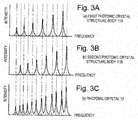
- Fig. 3A, Fig. 3B, and Fig. 3C Each of Fig. 3A to Fig. 3C is a graph whose horizontal axis is the frequency and whose vertical axis is the intensity of light.
- Fig. 3A shows a change of the intensity of light depending on the frequency, in the first PC structure formation body 11A, Fig.
- Fig. 3B shows the change in the second PC structure formation body 11B
- Fig. 3C shows the change in the photonic crystal 10 including the two bodies.
- a plurality of peaks respectively centering on the resonant frequencies appear in all of these graphs.
- the resonant frequencies are different.
- both the resonant frequencies of the first PC structure formation body 11A and the resonant frequencies of the second PC structure formation body 11B form the resonant frequencies of the photonic crystal 10 in Fig. 3C .
- the two bodies are spaced a little apart from each other, even if light having a resonant frequency of one of the PC structure formation bodies is introduced into the other of the PC structure formation bodies, light resonance concerning the one of the PC structure formation bodies can also be generated in the other of the PC structure formation bodies.
- the distance between the first PC structure formation body 11A and the second PC structure formation body 11B that is, the thickness of the spacer layer 15 be set to be shorter than the wavelength in the spacer layer 15, of light having the lowest frequency (largest wavelength) within the target frequency domain.
- the distance be set to be shorter than the wavelength in the spacer layer 15, of light having the highest frequency (smallest wavelength) within the target frequency domain.
- the two PC structure formation bodies have the same cycle length a.
- the cycle lengths of the two bodies may be set to different values a 1 and a 2 (a first modified example).
- the resonant wavelengths inside the two PC structure formation bodies have different values, and hence the resonant frequencies of the two PC structure formation bodies can be made different values even if the two bodies have the same thickness d.
- the two PC structure formation bodies have the same radius r of each hole 13.
- the radii of the holes of the two bodies may be set to different values r 1 and r 2 (a second modified example, a photonic crystal 10B).
- the average refractive indexes of the two PC structure formation bodies can be made different values, and hence the resonant frequencies of the two PC structure formation bodies can be made different values even if the two bodies have the same thickness d and the same cycle length a.
- the heights of the holes 13 of the two PC structure formation bodies may be set to different values h 1 and h 2 .
- a third PC structure formation body 11C is provided between the two PC structure formation bodies in the first embodiment.
- a thickness d 3 of the third PC structure formation body 11C has a value between d 1 and d 2 , and the holes 13 are formed in a square lattice pattern in the third PC structure formation body 11C with the same shape, the same size, and the same cycle length a as those formed in the other two PC structure formation bodies.
- standing waves whose wavelengths inside the third PC structure formation body 11C are the same as those of the other PC structure formation bodies and whose frequencies and wavelengths outside the photonic crystal are different therefrom are formed in the third PC structure formation body 11C. Accordingly, the photonic crystal of the third modified example can make the number of resonant frequencies further larger than that of the first embodiment.
- each hole 13 is not limited to a columnar shape, and various shapes (for example, a prismatic shape such as a triangular prism and a quadrangular prism (cuboid), a conical shape, a pyramidal shape such as a triangular pyramid and a quadrangular pyramid, a partial spherical shape, and a partial oval spherical shape) can be adopted.
- the arrangement cycle of the holes 13 is not limited to the square lattice pattern, and can be a triangular lattice pattern, a rectangular lattice pattern, an orthorhombic lattice pattern, and other lattice patterns.
- the materials of the first plate-like member 12A and the second plate-like member 12B are not limited to the above-mentioned ones, and any material can be adopted as long as the material enables light within a target frequency domain to propagate such that standing waves of the light within the frequency domain are formed in each PC structure formation body. Further, in addition to such a two-dimensional photonic crystal as described above formed by cyclically arranging modified refractive index regions in each plate-like member, photonic crystals in various forms, for example, a three-dimensional photonic crystal described in Patent Literature 4 can also be adopted.
- a member obtained by joining a p-type semiconductor layer 12AP and an n-type semiconductor layer 12AN may be used as the first plate-like member 12A
- a member obtained by joining a p-type semiconductor layer 12BP and an n-type semiconductor layer 12BN may be used as the second plate-like member 12B (a fourth modified example).
- a layer made of a conductor may be used for the spacer layer 15 ( Fig.
- a photonic crystal 10D a three-layer structure in which a first conductor layer 151, an insulator layer 153, and a second conductor layer 152 are laminated in the stated order may be used for the spacer layer 15 ( Fig. 7B , a photonic crystal 10E).
- Such photonic crystals can be used suitably for photoelectric conversion apparatuses to be described later.
- a photonic crystal 20 of the second embodiment is the same as the photonic crystal 10 of the first embodiment in that, as shown in Fig. 8A , the photonic crystal 20 has a configuration in which three layers of a first PC structure formation body 21A, a spacer layer 25, and a second PC structure formation body 21B are laminated in the stated order.
- the second embodiment is the same as the first embodiment in the thicknesses d 1 and d 2 (of the plate-like members) of the first PC structure formation body 21A and the second PC structure formation body 21B.
- a large number of holes 23 each having the radius r and the height h are provided in the first PC structure formation body 21A and the second PC structure formation body 21B.
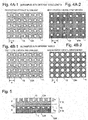
- Each hole 23 is arranged such that the center of the circle of its column is shifted by ⁇ p from each lattice point of the square lattice (as indicated by an alternate long and short dash line in Fig. 8B ).
- the amount of shift ⁇ p is distributed within a range of 0 to a maximum amount of shift ⁇ p max , and there is no rule for the distribution.
- the direction in which each hole 23 is shifted from each lattice point is not uniform, and there is no rule for the difference among the holes 23. That is, each hole 23 is arranged so as to be randomly shifted by the amount of shift ⁇ p equal to or less than the maximum amount of shift ⁇ p max ( ⁇ 0) from each lattice point of the square lattice.
- How the positions of the holes 23 are shifted when the first PC structure formation body 21A and the second PC structure formation body 21B are compared with each other may be the same between the two bodies, or may be different between the two bodies.
- each hole 23 is arranged so as to be randomly shifted from each lattice point of the square lattice, refractive index distribution to which randomness is introduced while a cyclic pattern is held to some extent is formed in a two-dimensional photonic crystal. Accordingly, with reference to a graph whose horizontal axis is the frequency and whose vertical axis is the intensity of light, the first PC structure formation body 21A and the second PC structure formation body 21B have peaks at a plurality of wavelengths corresponding to the basic cyclic pattern of the lattice points.
- each peak Due to the randomness, each peak has a smaller peak top height but has a larger width than those in the first embodiment, and hence the intensity is higher at each frequency that is away from the peak top to some extent ( Fig. 9A ).
- the number of resonant frequencies is larger than that in the case where an individual PC structure formation body is used, similarly to the photonic crystal of the first embodiment, and each peak has a smaller peak top height but has a larger width similarly to the PC structure formation bodies in the present embodiment. Because each peak width is larger in this way, the intensity of light inside the photonic crystal can be made higher than that in the first embodiment, in terms of the overall target frequency domain.
- each hole 23 is arranged so as to be randomly shifted from each lattice point, so that such a property that a change in absorption property with respect to a change in incident angle is smaller is obtained.
- adjacent holes may overlap with each other. If holes overlap with each other, a plurality of holes form one modified refractive index region, and hence the cyclic pattern of the square lattice is disturbed more than necessary. Moreover, at the point at which the profiles of the plurality of holes overlap with each other, the shape of the plate-like member of the PC structure formation body is pointed toward the hole, and such a shape is difficult to make, which is problematic. Hence, it is desirable to set the maximum amount of shift ⁇ p max such that adjacent holes are separated from (do not overlap with) each other, in consideration of the shapes and the sizes of the holes (modified refractive index regions).
- each hole 23A may be arranged at each lattice point of the square lattice, and the size, for example, the radius of each hole 23A may be randomly set within a range of r min to r max .
- each peak on a graph whose horizontal axis is the frequency and whose vertical axis is the intensity of light has a smaller peak top height but has a larger width, similarly to the photonic crystal 20 of the second embodiment, and hence the intensity of light inside the photonic crystal can be made higher in terms of the overall target frequency domain.
- the size of the hole 23A is defined as the radius in this example, the size of the hole 23A may be defined as the area, the volume, or the like. Also in this case, it is desirable to set r max such that adjacent holes are separated from (do not overlap with) each other.
- the first embodiment of the photoelectric conversion apparatus according to the present invention is described with reference to Fig. 11, Fig. 12A, Fig. 12B, and Fig. 12C .
- a photoelectric conversion apparatus 30 of the present embodiment is formed by sandwiching the photonic crystal 10 of the first embodiment between a plate-like transparent electrode 321 and a plate-like back-side electrode 322.
- the first plate-like member 12A constituting the photonic crystal 10 is made of the p-type silicon semiconductor, and the second plate-like member 12B constituting the same is made of the n-type silicon semiconductor.
- the photonic crystal 10 functions as a photoelectric conversion layer 31 formed through p-n junction with the electrically conductive spacer layer 15 being sandwiched between the two members 12A and 12B.
- This photoelectric conversion layer can absorb light within such a range that the wavelength in air is about 600 to 1,100 nm and the frequency is 2.7 ⁇ 10 14 to 5.0 ⁇ 10 14 Hz, and can convert the absorbed light into current.
- the thickness d 1 of the first plate-like member 12A is set to 700 nm
- the thickness d 2 of the second plate-like member 12B is set to 300 nm.
- the height h of each hole 13 is 260 nm
- the radius of each hole 13 is 200 nm
- the cycle length a of the square lattice is 700 nm.
- a thickness d 0 of the spacer layer 15 is 230 nm.
- the spacer layer 15 and the transparent electrode 321 are each made of ITO transparent to light within the above-mentioned frequency range, and the back-side electrode 322 is made of silver.
- the photoelectric conversion apparatus 30 of the first embodiment when light having a frequency within the above-mentioned range is made incident on the photoelectric conversion layer 31 from the transparent electrode 321 side, standing waves of light having frequencies corresponding to a large number of resonant frequencies in the photonic crystal 10 as the photoelectric conversion layer 31 are formed in the photonic crystal 10. Consequently, light having the resonant frequencies more easily stays in the photoelectric conversion layer 31, and are more easily absorbed by the photoelectric conversion layer 31 to be converted into current. As a result, the photoelectric conversion efficiency becomes higher.
- the number of resonant frequencies is larger than that in the case where only one similar PC structure formation body is provided, and therefore the photoelectric conversion efficiency can be made higher.
- Fig. 12A shows a result of calculating the light absorption rate of the photoelectric conversion layer 31 when sunlight is made incident on the photoelectric conversion apparatus 30 of the first embodiment, by means of a graph whose horizontal axis is the light wavelength in air.
- Fig. 12A also shows, as comparative examples, respective graphs of the light absorption rates in: a solar cell having a light incident surface that is provided with irregularities called Lambertian texture instead of a photonic crystal (a first comparative example); and a solar cell that is not provided with any of a photonic crystal and Lambertian texture (a second comparative example).
- the semiconductor materials forming the photoelectric conversion layer and the amounts of the materials were set to be the same, whereby conditions concerning light absorption, other than the holes of the photonic crystal and whether or not the texture structure existed, were equalized.
- the integrated absorption rate obtained by integrating and then normalizing each graph of the absorption rate over the entire target wavelength band was 43.0% in the first comparative example and 10.2% in the second comparative example, whereas this rate was 48.8% in the first embodiment, which was a value higher than those in the two comparative examples.
- light absorbed by the photonic crystal 10 in the photoelectric conversion apparatus 30 of the first embodiment is divided into light absorbed by the first PC structure formation body 11A ( Fig. 12B ) and light absorbed by the second PC structure formation body 11B ( Fig. 12C ), and the respective absorption rates of these rays of light are shown in graphs.
- Fig. 12B and Fig. 12C at a plurality of wavelengths indicated by vertical arrows in these graphs, light is hardly absorbed by the first PC structure formation body 11A, and is absorbed by the second PC structure formation body 11B with high efficiency.
- the number of wavelengths (resonant wavelengths, resonant frequencies) with a high absorption rate can be made larger than that in the case where only one PC structure formation body (first PC structure formation body 11A) is provided, whereby the absorption rate of the entire photoelectric conversion layer 31 can also be made higher.
- Fig. 13A and Fig. 13B respectively show, as modified examples of the photoelectric conversion apparatus of the first embodiment, a photoelectric conversion apparatus 30A including the photonic crystal 10D in the fourth modified example and a photoelectric conversion apparatus 30B including the photonic crystal 10E in the fourth modified example.
- both the first PC structure formation body 11A and the second PC structure formation body 11B have the configuration in which the p-type semiconductor layer and the n-type semiconductor are laminated, as described above, and function as photoelectric conversion apparatuses independently of each other.
- the spacer layer 15 has a role in connecting the two independent photoelectric conversion apparatuses in series.
- the first conductor layer 151 in the spacer layer 15 has a role as an electrode for injecting current into the first PC structure formation body 11A
- the second conductor layer 152 in the spacer layer 15 has a role as an electrode for injecting current into the second PC structure formation body 11B
- the insulator layer 153 has a role in electrically insulating the two photoelectric conversion layers from each other.
- a photoelectric conversion apparatus 40 of the second embodiment is formed by sandwiching the photonic crystal 20 of the second embodiment between a plate-like transparent electrode 421 and a plate-like back-side electrode 422.
- the materials of the transparent electrode 421 and the back-side electrode 422 are the same as those used in the photoelectric conversion apparatus of the first embodiment.
- the absorption rate for each wavelength and the integrated absorption rate were calculated for a plurality of values that are equal to or less than one and can be taken by the maximum amount of shift ⁇ p max in each of the first PC structure formation body 21A and the second PC structure formation body 21B.
- the value of the maximum amount of shift ⁇ p max is represented by the ratio to the cycle length of the holes. Conditions other than the maximum amount of shift ⁇ p max are the same as those in the photoelectric conversion apparatus of the first embodiment.
- Fig. 15 is a graph showing results of calculating the absorption rate for each wavelength within such a range that the maximum amount of shift ⁇ p max is 0.1 to 0.5. A plurality of peaks is found in this graph. Compared with the first embodiment ( Fig. 12A ), in the present embodiment, no sharp peak top is found, but each peak width is larger, and the absorption rate does not drop at a particular wavelength over the entire wavelength range for this calculation.
- Fig. 16 is a graph showing the relation between the integrated absorption rate and the maximum amount of shift ⁇ p max in the second embodiment.
- this graph also shows a result of calculation for the case where only one PC structure formation body is provided.
- the integrated absorption rate is higher over the entire range of ⁇ p max than that in the case where only one PC structure formation body is provided.
- ⁇ p max is equal to or less than 0.4, the integrated absorption rate is higher than that in the first embodiment.
- the photonic crystal of the present invention can be directly used as a light extraction element using a diffraction effect.
- a light guide plate 50 is described as a specific example of using the diffraction element according to the present invention.
- the light guide plate 50 is used for, for example, an edge-lit backlight unit in a liquid crystal display.
- the edge-lit backlight unit light is supplied to the entire back surface of a panel of the liquid crystal display through the light guide plate from a light source provided lateral to the panel, and the entire panel is irradiated with illumination light from the back surface.
- the light guide plate 50 of the present embodiment has a configuration in which a reflection plate 52 is provided to the surface of the second PC structure formation body 11B opposite to the spacer layer 15 in the photonic crystal 10.
- plastic such as acrylic, glass, and other materials that do not easily absorb visible light are used for the first plate-like member 12A and the second plate-like member 12B.
- the photonic crystal 10 has a role as a diffraction element 51.
- a light source 61 for visible light to be introduced into the diffraction element 51 is provided lateral to the light guide plate 50.
- the light source 61 is not a constituent element of the light guide plate 50, but constitutes a backlight unit together with the light guide plate 50.
- the light guide plate 50 of the present embodiment when visible light is introduced into the diffraction element 51 from the light source 61, standing waves of light are formed at a large number of frequencies corresponding to the resonant frequencies of the photonic crystal 10. These standing waves are scattered by the holes 13 to be eventually emitted to the outside of the photonic crystal 10 from two surfaces of the photonic crystal 10.
- light emitted on the side on which the reflection plate 52 is provided is reflected on the reflection plate 52, and hence all the rays of emitted light are emitted to the outside of the light guide plate 50 from the surface opposite to the side on which the reflection plate 52 is provided.
- light having a large number of frequencies corresponding to the resonant frequencies of the photonic crystal 10 can be scattered with high probability, and hence the light emission efficiency of a backlight can be made higher.
Landscapes
- Physics & Mathematics (AREA)
- Chemical & Material Sciences (AREA)
- Crystallography & Structural Chemistry (AREA)
- General Physics & Mathematics (AREA)
- Optics & Photonics (AREA)
- Optical Integrated Circuits (AREA)
- Photovoltaic Devices (AREA)
- Diffracting Gratings Or Hologram Optical Elements (AREA)
Applications Claiming Priority (2)
| Application Number | Priority Date | Filing Date | Title |
|---|---|---|---|
| JP2013086902 | 2013-04-17 | ||
| PCT/JP2014/060731 WO2014171457A1 (ja) | 2013-04-17 | 2014-04-15 | フォトニック結晶及びそれを利用した光機能デバイス |
Publications (2)
| Publication Number | Publication Date |
|---|---|
| EP2988152A1 true EP2988152A1 (de) | 2016-02-24 |
| EP2988152A4 EP2988152A4 (de) | 2016-08-24 |
Family
ID=51731395
Family Applications (1)
| Application Number | Title | Priority Date | Filing Date |
|---|---|---|---|
| EP14784909.5A Withdrawn EP2988152A4 (de) | 2013-04-17 | 2014-04-15 | Photonischer kristall und optische funktionsvorrichtung damit |
Country Status (6)
| Country | Link |
|---|---|
| US (1) | US10866343B2 (de) |
| EP (1) | EP2988152A4 (de) |
| JP (1) | JP6163542B2 (de) |
| CN (1) | CN105143923B (de) |
| TW (1) | TWI625539B (de) |
| WO (1) | WO2014171457A1 (de) |
Cited By (4)
| Publication number | Priority date | Publication date | Assignee | Title |
|---|---|---|---|---|
| CN106226846A (zh) * | 2016-09-07 | 2016-12-14 | 山东科技大学 | 一种基于反转压印纳米成型技术的力响应性光子晶体材料的制备方法 |
| CN106226847A (zh) * | 2016-09-07 | 2016-12-14 | 山东科技大学 | 一种力响应性纳米量级光子晶体材料的制备方法 |
| CN106291776A (zh) * | 2016-09-07 | 2017-01-04 | 山东科技大学 | 一种基于纳米成型技术的力响应性光子晶体材料的制备方法 |
| CN121038447A (zh) * | 2025-10-31 | 2025-11-28 | 深圳市华宝新能源股份有限公司 | 一种光转换玻纤复合板及其制备方法和应用 |
Families Citing this family (9)
| Publication number | Priority date | Publication date | Assignee | Title |
|---|---|---|---|---|
| JP6281869B2 (ja) * | 2014-02-27 | 2018-02-21 | 国立大学法人大阪大学 | 方向性結合器および合分波器デバイス |
| TWI732746B (zh) | 2014-11-17 | 2021-07-11 | 日商迪睿合股份有限公司 | 異向性導電膜之製造方法 |
| SG11201805787YA (en) * | 2016-03-24 | 2018-10-30 | Illumina Inc | Photonic superlattice-based devices and compositions for use in luminescent imaging, and methods of using the same |
| DE102018107615B4 (de) * | 2017-09-06 | 2024-08-22 | OSRAM Opto Semiconductors Gesellschaft mit beschränkter Haftung | Verfahren zur Herstellung eines optoelektronischen Halbleiterchips und optoelektronischer Halbleiterchip |
| CN109273501B (zh) * | 2018-09-25 | 2020-08-21 | 京东方科技集团股份有限公司 | 柔性基底及其制造方法、显示装置 |
| CN109581579B (zh) | 2019-01-31 | 2021-03-05 | 京东方科技集团股份有限公司 | 一种导光板及其制作方法,以及背光模组和显示面板 |
| KR20220114407A (ko) * | 2021-02-08 | 2022-08-17 | 삼성전자주식회사 | 빔 확대필름 및 이를 포함하는 홀로그래픽 디스플레이 장치 |
| US20240128717A1 (en) * | 2021-02-25 | 2024-04-18 | Kyoto University | Two-dimensional photonic crystal laser |
| WO2024260793A1 (en) * | 2023-06-19 | 2024-12-26 | Ams-Osram Asia Pacific Pte. Ltd. | Angular broadband nanostructured optics |
Family Cites Families (23)
| Publication number | Priority date | Publication date | Assignee | Title |
|---|---|---|---|---|
| JPH01122762A (ja) | 1987-11-04 | 1989-05-16 | Nippon Abs Ltd | アンチスキッドブレーキ装置 |
| JPH07122762A (ja) * | 1993-10-22 | 1995-05-12 | Asahi Chem Ind Co Ltd | 薄膜光起電力装置 |
| JP2001074955A (ja) | 1999-08-31 | 2001-03-23 | Susumu Noda | フォトニック結晶導波路 |
| US6829281B2 (en) * | 2002-06-19 | 2004-12-07 | Finisar Corporation | Vertical cavity surface emitting laser using photonic crystals |
| US20050056312A1 (en) * | 2003-03-14 | 2005-03-17 | Young David L. | Bifacial structure for tandem solar cells |
| EP1724887A1 (de) | 2004-03-05 | 2006-11-22 | President, Kyoto University | Oberflächenemittierende laserlichtquelle mit zweidimensionalem photonischem kristall |
| WO2007029661A1 (ja) | 2005-09-05 | 2007-03-15 | Kyoto University | 2次元フォトニック結晶面発光レーザ光源 |
| US7697584B2 (en) * | 2006-10-02 | 2010-04-13 | Philips Lumileds Lighting Company, Llc | Light emitting device including arrayed emitters defined by a photonic crystal |
| ES2277800B2 (es) * | 2007-02-16 | 2009-02-16 | Universidad Politecnica De Madrid | Dispositivo para acoplar la luz de forma optima a una celula solar de banda intermedia realizada mediante puntos cuanticos. |
| JP4928321B2 (ja) * | 2007-03-26 | 2012-05-09 | 独立行政法人科学技術振興機構 | 発光素子 |
| JP5070161B2 (ja) * | 2007-08-31 | 2012-11-07 | 独立行政法人科学技術振興機構 | フォトニック結晶レーザ |
| US20100282304A1 (en) * | 2008-11-18 | 2010-11-11 | Industrial Technology Research Institute | Solar cell and method of manufacturing the same |
| JP5667747B2 (ja) | 2009-03-18 | 2015-02-12 | 株式会社東芝 | 薄膜太陽電池およびその製造方法 |
| WO2011083674A1 (ja) * | 2010-01-07 | 2011-07-14 | シャープ株式会社 | 光電変換素子 |
| CN102714233A (zh) | 2010-01-07 | 2012-10-03 | 夏普株式会社 | 光电转换元件 |
| WO2011083693A1 (ja) * | 2010-01-07 | 2011-07-14 | シャープ株式会社 | 太陽電池、太陽電池パネルおよび太陽電池を備えた装置 |
| WO2011102956A2 (en) * | 2010-02-22 | 2011-08-25 | University Of Delaware | Photonic crystal enhanced light trapping solar cell |
| JP5518541B2 (ja) | 2010-03-26 | 2014-06-11 | 富士フイルム株式会社 | ナノ粒子の製造方法及び量子ドットの製造方法 |
| TWI543386B (zh) * | 2011-03-28 | 2016-07-21 | 財團法人工業技術研究院 | 圓形光子晶體結構、發光二極體元件以及光電轉換元件 |
| WO2012141141A1 (ja) * | 2011-04-14 | 2012-10-18 | シャープ株式会社 | 太陽電池、太陽電池パネルおよび太陽電池を備えた装置 |
| JP5794687B2 (ja) | 2011-08-12 | 2015-10-14 | 国立大学法人京都大学 | フォトニック結晶面発光レーザ |
| JP5842268B2 (ja) * | 2012-01-31 | 2016-01-13 | 国立大学法人京都大学 | 太陽電池 |
| JP5854383B2 (ja) * | 2012-01-31 | 2016-02-09 | 国立大学法人京都大学 | 2次元フォトニック結晶 |
-
2014
- 2014-04-15 EP EP14784909.5A patent/EP2988152A4/de not_active Withdrawn
- 2014-04-15 JP JP2015512489A patent/JP6163542B2/ja not_active Expired - Fee Related
- 2014-04-15 CN CN201480021934.1A patent/CN105143923B/zh not_active Expired - Fee Related
- 2014-04-15 US US14/784,862 patent/US10866343B2/en not_active Expired - Fee Related
- 2014-04-15 WO PCT/JP2014/060731 patent/WO2014171457A1/ja not_active Ceased
- 2014-04-17 TW TW103113993A patent/TWI625539B/zh not_active IP Right Cessation
Cited By (4)
| Publication number | Priority date | Publication date | Assignee | Title |
|---|---|---|---|---|
| CN106226846A (zh) * | 2016-09-07 | 2016-12-14 | 山东科技大学 | 一种基于反转压印纳米成型技术的力响应性光子晶体材料的制备方法 |
| CN106226847A (zh) * | 2016-09-07 | 2016-12-14 | 山东科技大学 | 一种力响应性纳米量级光子晶体材料的制备方法 |
| CN106291776A (zh) * | 2016-09-07 | 2017-01-04 | 山东科技大学 | 一种基于纳米成型技术的力响应性光子晶体材料的制备方法 |
| CN121038447A (zh) * | 2025-10-31 | 2025-11-28 | 深圳市华宝新能源股份有限公司 | 一种光转换玻纤复合板及其制备方法和应用 |
Also Published As
| Publication number | Publication date |
|---|---|
| TW201501339A (zh) | 2015-01-01 |
| CN105143923B (zh) | 2018-03-09 |
| CN105143923A (zh) | 2015-12-09 |
| WO2014171457A1 (ja) | 2014-10-23 |
| US10866343B2 (en) | 2020-12-15 |
| EP2988152A4 (de) | 2016-08-24 |
| JP6163542B2 (ja) | 2017-07-12 |
| TWI625539B (zh) | 2018-06-01 |
| JPWO2014171457A1 (ja) | 2017-02-23 |
| US20160061994A1 (en) | 2016-03-03 |
Similar Documents
| Publication | Publication Date | Title |
|---|---|---|
| US10866343B2 (en) | Photonic crystal and optical functional device including the same | |
| KR100706493B1 (ko) | 면광원 장치 및 표시 장치 | |
| US8779424B2 (en) | Sheet and light-emitting device | |
| JP5967592B2 (ja) | 光電変換素子 | |
| CN102792456B (zh) | 太阳能电池、太阳能电池板和具备太阳能电池的装置 | |
| US20090266413A1 (en) | Photovoltaic Cells With Gratings For Scattering Light Into Light-absorption Layers | |
| Foldyna et al. | Theoretical short-circuit current density for different geometries and organizations of silicon nanowires in solar cells | |
| JP5854383B2 (ja) | 2次元フォトニック結晶 | |
| JP6146627B2 (ja) | 太陽電池モジュール | |
| CN104867991B (zh) | 一种二维硅基光子晶体太阳能电池 | |
| KR101074782B1 (ko) | 염료감응 태양전지 모듈 | |
| JP6120450B2 (ja) | 太陽電池モジュールおよび太陽光発電装置 | |
| KR101661223B1 (ko) | 태양전지 | |
| CN102375914A (zh) | 一种利用二维光子晶体提高c波段led出光效率的方法 | |
| JP5842268B2 (ja) | 太陽電池 | |
| US20190081456A1 (en) | Semiconductor laser device | |
| US8872973B2 (en) | Light guiding sysetm, edge type backlight module and liquid display device | |
| US20130291934A1 (en) | Thin film solar cell structure | |
| US10340842B2 (en) | Multi-orthogonal photonic energy collection system | |
| JP2014013306A (ja) | 集光素子及び太陽電池システム | |
| Sturmberg et al. | Positional disorder in nanowire array photovoltaics | |
| de Sterke et al. | Total absorption in Structured Ultrathin Semiconductor Layers | |
| Seassal et al. | Absorption in photonic crystals: from order to disorder | |
| JP2013243305A (ja) | 太陽電池モジュールおよび太陽光発電装置 |
Legal Events
| Date | Code | Title | Description |
|---|---|---|---|
| PUAI | Public reference made under article 153(3) epc to a published international application that has entered the european phase |
Free format text: ORIGINAL CODE: 0009012 |
|
| 17P | Request for examination filed |
Effective date: 20151027 |
|
| AK | Designated contracting states |
Kind code of ref document: A1 Designated state(s): AL AT BE BG CH CY CZ DE DK EE ES FI FR GB GR HR HU IE IS IT LI LT LU LV MC MK MT NL NO PL PT RO RS SE SI SK SM TR |
|
| AX | Request for extension of the european patent |
Extension state: BA ME |
|
| RIC1 | Information provided on ipc code assigned before grant |
Ipc: G02B 5/18 20060101ALI20160316BHEP Ipc: G02B 1/02 20060101AFI20160316BHEP Ipc: H01L 31/0352 20060101ALI20160316BHEP |
|
| RIN1 | Information on inventor provided before grant (corrected) |
Inventor name: NODA, SUSUMU Inventor name: OSKOOI, ARDAVAN Inventor name: TANAKA, YOSHINORI |
|
| DAX | Request for extension of the european patent (deleted) | ||
| A4 | Supplementary search report drawn up and despatched |
Effective date: 20160725 |
|
| RIC1 | Information provided on ipc code assigned before grant |
Ipc: G02B 5/18 20060101ALI20160718BHEP Ipc: G02B 1/02 20060101AFI20160718BHEP Ipc: H01L 31/0352 20060101ALI20160718BHEP |
|
| STAA | Information on the status of an ep patent application or granted ep patent |
Free format text: STATUS: EXAMINATION IS IN PROGRESS |
|
| 17Q | First examination report despatched |
Effective date: 20191205 |
|
| STAA | Information on the status of an ep patent application or granted ep patent |
Free format text: STATUS: THE APPLICATION IS DEEMED TO BE WITHDRAWN |
|
| 18D | Application deemed to be withdrawn |
Effective date: 20240308 |