EP2988204A1 - Système et procédé d'extension de mémoire - Google Patents
Système et procédé d'extension de mémoire Download PDFInfo
- Publication number
- EP2988204A1 EP2988204A1 EP14814662.4A EP14814662A EP2988204A1 EP 2988204 A1 EP2988204 A1 EP 2988204A1 EP 14814662 A EP14814662 A EP 14814662A EP 2988204 A1 EP2988204 A1 EP 2988204A1
- Authority
- EP
- European Patent Office
- Prior art keywords
- processor
- extended
- memory
- identification number
- installation position
- Prior art date
- Legal status (The legal status is an assumption and is not a legal conclusion. Google has not performed a legal analysis and makes no representation as to the accuracy of the status listed.)
- Withdrawn
Links
Images



Classifications
-
- G—PHYSICS
- G06—COMPUTING OR CALCULATING; COUNTING
- G06F—ELECTRIC DIGITAL DATA PROCESSING
- G06F13/00—Interconnection of, or transfer of information or other signals between, memories, input/output devices or central processing units
- G06F13/38—Information transfer, e.g. on bus
- G06F13/42—Bus transfer protocol, e.g. handshake; Synchronisation
- G06F13/4204—Bus transfer protocol, e.g. handshake; Synchronisation on a parallel bus
- G06F13/4234—Bus transfer protocol, e.g. handshake; Synchronisation on a parallel bus being a memory bus
-
- G—PHYSICS
- G06—COMPUTING OR CALCULATING; COUNTING
- G06F—ELECTRIC DIGITAL DATA PROCESSING
- G06F13/00—Interconnection of, or transfer of information or other signals between, memories, input/output devices or central processing units
- G06F13/38—Information transfer, e.g. on bus
- G06F13/40—Bus structure
- G06F13/4004—Coupling between buses
- G06F13/4027—Coupling between buses using bus bridges
Definitions
- the present application relates to the field of information storage technologies, and in particular, to a memory extension system and method.
- a computing capability of a processor, a memory capacity, and a bandwidth of an input/output interface are three important indicators for evaluating performance of a computer system.
- a high-performance processor for example, a multi-core multi-thread processor
- multiple processors are interconnected in most cases to form an SMP (Symmetrical Multi Processing, symmetric multiprocessor) or NUMA (Non Uniform Memory Access, non-uniform memory access) architecture to implement concurrent processing of a service.
- SMP Symmetrical Multi Processing, symmetric multiprocessor
- NUMA Non Uniform Memory Access, non-uniform memory access
- a processor generally integrates multiple memory controllers, and each controller can support multiple memory modules.
- the memory capacity may be extended to a scale of several hundreds of GB.
- PCI Express Peripheral Component Interconnect Express, Peripheral Interconnect Standard Bus
- RapidIO Peripheral Interconnect Standard Bus
- 10G Ethernet interfaces in the recent decade, and a rate constantly increases with upgrading of a protocol version.
- the computing capability, the memory capacity, and the bandwidth of the input/output interface should be configured in a balanced manner; otherwise, a performance bottleneck easily occurs, which affects overall performance of the computer system.
- servers used for different types of services such as a Web server, a database server, and a streaming media server
- the computing capability of the processor is of the utmost importance, and the memory capacity is relatively not so pressing.
- a virtualization application scenario because multiple services need to be deployed on multiple cores of the same processor and certain memory space needs to be allocated for each service, a more pressing requirement is imposed on the memory capacity.
- a current server generally uses a universal multi-way processor design.
- the server may support multiple services, a service to be specifically performed is determined by a customer, for example, different application programs are installed to complete different service functions. Therefore, the server may have certain redundancy in a processing capability or a memory capacity, which increases a hardware cost and operating power consumption.
- a processor integrates a memory controller that can be externally connected to a memory module.
- a memory capacity requirement may exceed a capacity of memories that come with the two processors. If the other two processors are also installed, the cost and power consumption increases; but if the other two processors are not installed, the memory capacity is insufficient.
- the present application provides a memory extension system and method to solve a problem of processing capability redundancy in the prior art caused due to that a processor is added to extend a memory capacity.
- the present application provides a memory extension system, and the system includes a processor, an extended memory, an extended chip, and multiple processor installation positions, where a memory installation position that is connected to the processor installation position is provided in each of the processor installation positions; the multiple processor installation positions are connected through a QuickPath Interconnect QPI interface, the processor is installed in at least one processor installation position, and at least one of the other processor installation positions is used as an extended installation position; the extended chip is installed in at least one extended installation position, where the extended chip has a unique identification number; and the extended memory is installed in a memory installation position that is connected to the extended chip, and all addresses of the extended memory are within an address space range of the processor.
- a pin of the extended chip is compatible with a pin of the processor.
- the processor includes: a query instruction generating module, configured to generate an identification number query instruction; a query instruction sending module, configured to send the identification number query instruction through a QPI interface in the processor installation position in which the processor is located; an identification number receiving module, configured to receive an identification number through the QPI interface in the processor installation position in which the processor is located; an identification number determining module, configured to determine whether a received identification number is an identification number of the extended chip; and a configuring module, configured to, when the identification number is an identification number of the extended chip, configure a memory controller for the extended chip, and allocate, from the address space of the processor, a memory address corresponding to the extended memory that is connected to the extended chip.
- the processor further includes: a packet generating module, configured to generate a packet that is used for reading data or writing data and whose protocol is the QPI protocol; a packet sending module, configured to send the packet through the QPI interface in the processor installation position in which the processor is located; and a data receiving module, configured to receive, through the QPI interface in the processor installation position in which the processor is located, data that is read by the extended chip according to the packet.
- a packet generating module configured to generate a packet that is used for reading data or writing data and whose protocol is the QPI protocol
- a packet sending module configured to send the packet through the QPI interface in the processor installation position in which the processor is located
- a data receiving module configured to receive, through the QPI interface in the processor installation position in which the processor is located, data that is read by the extended chip according to the packet.
- the extended chip includes: a query instruction receiving module, configured to receive the identification number query instruction through a QPI interface in the extended installation position in which the extended chip is located; an identification number acquiring module, configured to acquire the identification number of the extended chip according to the identification number query instruction; and an identification number sending module, configured to send the acquired identification number through the QPI interface in the extended installation position in which the extended chip is located.
- the extended chip further includes a QPI interface module, a protocol converting module, and a memory interface module, where the QPI interface module is connected to the QPI interface in the extended installation position in which the extended chip is located, and is configured to receive the packet that is sent by the processor and whose protocol is the QPI protocol; the protocol converting module is configured to convert the packet of the QPI protocol into a packet of a memory interface protocol and send the packet of the memory interface protocol to the memory interface module; the memory interface module is connected to the extended memory in the memory installation position in the extended installation position in which the extended chip is located, and is configured to read data from or write data into the extended memory according to the packet obtained after the protocol conversion, and send the read data to the protocol converting module; and the protocol converting module is further configured to convert the read data from the memory interface protocol into the QPI protocol and send the data to the QPI interface module, and the QPI interface module is further configured to send the data obtained after
- the present application provides a memory extension method, where the method includes: generating, by a processor, an identification number query instruction, and sending the identification number query instruction through a QuickPath Interconnect QPI interface in a processor installation position in which the processor is located; receiving, by an extended chip, the query instruction through a QPI interface in a processor installation position in which the extended chip is located, acquiring an identification number of the extended chip according to the identification number query instruction, and sending the acquired identification number through the QPI interface in the processor installation position in which the extended chip is located; and receiving, by the processor, the identification number through the QPI interface in the processor installation position in which the processor is located, determining whether the identification number is an identification number of the extended chip, and when the identification number is an identification number of the extended chip, configuring a memory controller for the extended chip, and allocating, from address space of the processor, a memory address corresponding to an extended memory that is connected to the extended chip.
- the method further includes: determining, by the processor, whether to send the identification number query instruction to all QPI interfaces in the processor installation position in which the processor is located; and if it is determined that the identification number query instruction is not sent to all QPI interfaces in the processor installation position in which the processor is located, sending, by the processor, the identification number query instruction to a QPI interface to which the identification number query instruction has not been sent.
- the method further includes: generating, by the processor, a packet that is used for reading data or writing data and whose protocol is the QPI protocol, and sending the packet through the QPI interface in the processor installation position in which the processor is located; receiving, by the extended chip, the packet through the QPI interface in the processor installation position in which the extended chip is located, after the packet is converted from the QPI protocol into a memory interface protocol, reading data from or writing data into the extended memory that is connected to the extended chip according to the packet obtained after the protocol conversion, and sending, after the read data is converted from the memory interface protocol into the QPI protocol, the read data through the QPI interface in the processor installation position in which the extended chip is located; and receiving, by the processor, the data obtained after the protocol conversion through the QPI interface in the processor installation position in which the processor is located.
- a processor is provided in some processor installation positions and an extended chip is provided in other processor installation positions.
- the processor and the extended chip perform a data interaction through a QPI interface between the processor installation positions.
- Each extended chip can separately connect to an extended memory of the extended chip.
- the processor can access the extended memory connected to each extended chip by using the extended chip.
- this memory extension system uses an extended chip that is installed in another processor installation position to replace a processor, so that an existing processor can access an extended memory of the extended chip by using the extended chip.
- a memory capacity of the existing processor increases while a processing capability does not increase, which avoids a problem of processing capability redundancy in the prior art caused due to that a processor is added to extend a memory capacity.
- the following embodiments of the present application provide a memory extension system and method.
- the memory extension system is in a system of a multi-way processor design.
- an extended chip may be installed in another processor installation position to replace a processor, and a needed extended memory may be installed in a memory installation position of a processor installation position in which the extended chip is located.
- an existing processor may communicate with the extended chip through a QPI interface, to implement an access to the extended memory that is connected to the extended chip.
- FIG. 1 is a schematic structural diagram of a memory extension system according to this embodiment of the present application.
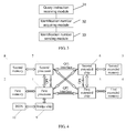
- the memory extension system may include a first processor 1, a first memory 2, a first extended chip 3, a first extended memory 4, a second extended memory 5, and a second extended chip 6.
- the first processor 1, the first extended chip 3, and the second extended chip 6 are respectively installed in the three processor installation positions (not shown in the diagram).
- the three processor installation positions are connected through a QPI (Quick Path Interconnect, QuickPath Interconnect) interface.
- the first memory 2 is a memory that comes with the first processor 1.
- the first extended memory 4 is connected to the first extended chip 3.
- the second extended memory 5 is connected to the second extended chip 6.
- a processor installation position in which the first processor 1 is located may be referred to as a first processor installation position
- a processor installation position in which the first extended chip 3 is located may be referred to as a first extended installation position
- a processor installation position in which the second extended chip 6 is located is referred to as a second extended installation position.
- the first processor 1 may be directly welded in the first processor installation position.
- the first processor 1 may also be installed in the first processor installation position through a pluggable interface.
- the pluggable interface may be a pin and a socket that match each other, or a plug-in card and a slot that match each other.
- the first extended chip 3 and/or the second extended chip 6 may be fixed in a corresponding extended installation position in a manner of welding, and certainly, for ease of disassembly or assembly of the multiprocessor system, may also connect to a corresponding extended installation position in a manner of a pluggable interface.
- Data interaction is performed between the three processor installation positions through the QPI interface.
- the QPI interface is formed by 20 pairs of differential transmitted signals, 20 pairs of differential received signals, and 2 pairs of differential clock signals. A signal rate may reach 6.4 GT/s and a bidirectional bandwidth may be 25.6 GB/s.
- the QPI interface also supports consistency of a cache, and may perform a configuration access to a peripheral device and read and write operations on a memory.
- One or more memory installation positions are provided in each processor installation position to increase memory space.
- the first memory 2 is installed in the memory installation position in the first processor installation position
- the first extended memory 4 is installed in the memory installation position in the first extended installation memory
- the second extended memory 5 is installed in the memory installation position in the second extended installation position.
- a processor installation position is connected to a memory installation position that is connected through a memory interface, and a protocol format for data interaction between the processor installation position and the memory installation position that is connected is a memory interface protocol format.
- Each extended chip has a unique identification number. By using the identification number, it may be identified whether a component in a processor installation position is an extended chip.
- Each extended chip may connect to one or more extended memories, and addresses of all extended memories that connect to the extended chip are within an address space range of the first processor 1.
- a pin of each extended chip is compatible with a pin of the processor.
- the following pin specifications of an extended chip may be compatible with a pin of the processor:
- 9 is a bridge chip and 10 is a BIOS (Basic Input Output System, basic input/output system).
- the first processor 1 is connected to the bridge chip 9 (generally referred to as a southbridge) through a DMI interface (Direct Media Interface, direct media interface).
- the first processor 1 may access the BIOS 10 by using the bridge chip 9.
- the first processor 1 that may access the bridge chip 9 is referred to as a master processor, and another processor is referred to as a slave processor (no slave processor is set in the embodiment shown in FIG. 1 ).
- the master processor After each power reset ends, the master processor always starts first, performs initialization for a peripheral device, and then controls a slave processor to start.
- FIG.2 is a schematic structural diagram of the first processor according to this embodiment of the present application.
- the first processor 1 may include:
- FIG. 3 is a schematic structural diagram of the extended chip according to this embodiment of the present application.
- the extended chip may include:
- the first processor 1 may then perform initialization for the extended chip.
- the number of processors is 1 is used as an example.
- the number of processors may be set freely according to a requirement of a system for a computing capability, which may be two or more. When there are multiple processors, more QPI interfaces need to be provided by the processors.
- FIG. 4 is another schematic structural diagram of the memory extension system according to this embodiment of the present application.
- the memory extension system may further include a second processor 7 and a second memory 8.
- a processor installation position in which the second processor 7 is located is a second processor installation position
- the second memory 8 is a memory that comes with the second processor 7.
- the first processor 1 directly is connected to the second processor 7 through a QPI interface. Both processors integrate a memory controller, and each processor may externally connect to one or more memories that belong to the processor. In addition, both processors support mutual accesses to the memories of each other.
- the first processor 1 may be referred to as a master processor
- the second processor 2 may be referred to as a slave processor.
- the master processor After power-on or a reset of the system ends, the master processor starts first, and executes code of a BIOS. After completing initialization of a peripheral device and preparing startup code for the slave processor, the master processor controls another slave processor to start, and then loads an operating system and starts to run the operating system on all processors.
- the first processor 1 may access the extended memory of the extended chip after completing initialization of the peripheral device and successfully loading the operating system.
- the first processor 1 may further include:
- the extended chip may further include a QPI interface module 61, a protocol converting module 62, and a memory interface module 63.
- the QPI interface module 61 is connected to the QPI interface in the extended installation position in which the extended chip is located, and is configured to receive the packet that is sent by the first processor and whose protocol is the QPI protocol. Because data interaction between processor installation positions is performed through the QPI interface, the packet sent by the first processor is in a QPI protocol format.
- the protocol converting module 62 is configured to convert the packet of the QPI protocol into a packet of a memory interface protocol and send the packet to the memory interface module 63.
- the extended chip and the extended memory connect to each other through a memory interface, that is, data interaction between the two is performed in a memory interface protocol format. Therefore, after receiving the packet in the QPI protocol format sent from the QPI interface, the protocol converting module 62 first parses the packet according to the QPI protocol to identify information included in the packet: a memory address to access, an access type (read or write), data length, and data to be written (for a write operation), and after converting the identified information into the memory interface protocol format, send the information to the memory interface module 63 so that the memory interface module 63 then sends the information to the extended memory.
- the protocol converting module 62 is further configured to convert the received data into the QPI protocol format, so that the QPI interface module 61 sends the data in the QPI protocol format to the first processor 1.
- the memory interface module 63 is connected to the extended memory in the memory installation position in the extended installation position in which the extended chip is located, and is configured to read data from or write data into the extended memory according to the packet obtained after the protocol conversion, and send the read data to the protocol converting module 62.
- a processor is provided in some processor installation positions and an extended chip is provided in other processor installation positions.
- the processor and the extended chip perform a data interaction through a QPI interface between the processor installation positions.
- Each extended chip can separately connect to an extended memory, and the processor can access the extended memory connected to each extended chip.
- this memory extension system uses an extended chip that is installed in another processor installation position to replace a processor, and accesses an extended memory of the extended chip by using the extended chip.
- an extended chip is mainly used to perform protocol conversion, and has low costs and power consumption. Therefore, in the memory extension system provided by this embodiment of the present application, increase of a memory capacity may be implemented at low costs and power consumption.
- a first processor is used as an example for description, and a first extended chip and a second extended chip are affiliated to the first processor.
- each extended chip may establish an association with different processors.
- a second extended chip may be affiliated to a first processor, and may also be affiliated to a second processor.
- a first extended chip is the same.
- the second processor has an affiliated extended chip, for a structure of the second processor, refer to a structure of the first processor described in the foregoing embodiment, which is not described herein again.
- a correspondence between an extended chip and a processor may be freely set according to an actual use situation.
- the first extended chip and the second extended chip both belong to the first processor. Then, specific design is required for software design and control of the first processor. For example, the first processor implements control over the second processor by controlling whether to allow the second processor to detect the extended chip.
- FIG. 7 is a schematic flowchart of a memory extension method according to this embodiment of the present application.
- the memory extension method may include the following:
- the processor sends the generated identification number query instruction through a QPI interface in a processor installation position in which the processor is located, and the identification number query instruction is used to determine an extended chip that is connected to the processor installation position in which the processor is located.
- An extended chip receives the identification number query instruction, acquires an identification number of the extended chip according to the identification number query instruction, and sends the acquired identification number.
- each extended chip may receive the identification number query instruction sent by the processor through the QPI interface in a processor installation position in which the extended chip is located. According to the identification number query instruction, the extended chip may query an identification number stored in the extended chip itself, and return the queried identification number to the processor through the QPI interface in the processor installation position in which the extended chip is located.
- the processor receives the identification number, determines whether the identification number is an identification number of the extended chip, and when the identification number is an identification number of the extended chip, configures a memory controller for the extended chip, and allocates, from address space of the processor, a memory address corresponding to an extended memory that is connected to the extended chip.
- a processor sends an identification number query instruction to all QPI interfaces on a processor installation position in which the processor is located, and receives a returned identification number.
- the processor may confirm an extended chip that is connected to the processor installation position in which the processor is located.
- the processor may perform initialization operations on the extended chip and an extended memory that is connected to the extended chip, including configuring a memory controller for the extended chip and allocating address space to the extended memory, where, the operation of configuring a memory controller may enable the processor to perform operations such as data reading or writing on the extended memory that is connected to the extended chip; the operation of allocating address space to the extended memory may map the extended memory into a part of memory space of the processor.
- the processor may access the extended memory that is connected to the extended chip. Certainly, the processor may also perform an initialization operation on a memory that comes with the processor. For example, in FIG. 1 , the memory that comes with the first processor 1 is the first memory 2, and the first processor 1 may configure a memory controller for the first memory 2 and allocate address space for the first memory 2.
- FIG. 8 is another schematic flowchart of the memory extension method according to this embodiment of the present application.
- the memory extension method may further include the following:
- the first processor generates, inside the first processor, the packet for reading data or writing data according to a data reading or writing requirement, and sends the packet through a QPI interface that is in a first processor installation position and is connected to the extended chip. Because data interaction between processor installation positions is performed through the QPI interface, the generated packet for reading data or writing data is in a QPI protocol format.
- the extended chip receives the packet, after the packet is converted from the QPI protocol into a memory interface protocol, reads data from or writes data into the extended memory according to the packet obtained after the protocol conversion, and after the read data is converted from the memory interface protocol data into the QPI protocol, sends the data.
- the extended chip receives the packet sent by the first processor 1 through a QPI interface in an extended installation position in which the extended chip is located.
- the packet sent by the first processor is in the QPI protocol format, and the extended chip and the extended memory connect to each other through a memory interface, that is, data interaction between the two is performed in a memory interface protocol format. Therefore, after receiving the packet in the QPI protocol format, the extended chip first parses the packet according to the QPI protocol to identify information included in the packet: a memory address to access, an access type (read or write), data length, and data to be written (for a write operation), and after converting the identified information into the memory interface protocol format, send the information to the extended memory to read data from or write data into the extended memory. After data is read from the extended memory, the extended chip receives data sent by the extended memory, converts the data into the QPI protocol format, and sends the data to the first processor 1 through the QPI interface in the extended installation position in which the extended chip is located.
- the extended chip is mainly used to perform protocol conversion. Compared with the prior art in which a new processor needs to be installed to increase a memory capacity, a manner of installing an extended chip to increase a memory capacity significantly reduces costs, and in addition, power consumption of the extended chip is very low compared with that of a processor.
- S203 The first processor receives the data sent by the extended chip.
- the first processor 1 receives the data in the QPI protocol format sent by the extended chip through the QPI interface in the first processor installation position.
- an identification number of an extended chip that is connected to a processor is searched, so that initialization operations are performed on the extended chip, including configuring a memory controller for the extended chip, allocating, from address space of the processor, a corresponding memory address to an extended memory, and loading a startup program into the extended memory. Therefore, when the processor needs to read or write data, the processor may directly access the extended memory that is connected to the extended chip by using the extended chip, that is, a problem that a processing capability is redundant may be resolved at relatively low costs and power consumption.
- the first processor 1 serves as a master processor and the second processor 7 serves as a slave processor.
- the processor 1 that serves as the master processor may further perform steps shown in FIG. 9 :
- S302 Query an identification number through a QPI interface.
- step S303 Determine whether the identification number is an identification number of the extended chip. If the identification number is an identification number of the extended chip, perform step S304; if the identification number is not an identification number of the extended chip, go to step S305.
- S304 Configure a memory controller for the extended chip and allocate corresponding memory space to the extended memory.
- step S305 Determine whether all QPI interfaces in the first processor installation position have been traversed. If all QPI interfaces in the first processor installation position have been traversed, perform step S306; if not all QPI interfaces in the first processor installation position have been traversed, go to step S302.
- a peripheral device that is, an extended chip
- startup code may be prepared for another slave processor to control the another slave processor to start.
- the first processor loads the operating system and runs the operating system.
- the first processor may access the extended memory that is connected to the extended chip.
- the software product is stored in a storage medium, and includes several instructions for instructing a computer device (which may be a personal computer, a server, or a network device) to perform all or a part of the steps of the methods described in the embodiments of the present application.
- the foregoing storage medium includes: any medium that can store program code, such as a read-only memory (ROM), a random access memory (RAM), a magnetic disk, or an optical disc.
- the present application may be applied to various general or dedicated computing system environments or configurations, for example, a personal computer, a server computer, a handheld device or portable device, a tablet device, a multiprocessor system, a microprocessor-based system, a set-top box, a programmable consumer electronic device, a network PC, a mini computer, a mainframe computer, and a distributed computing environment that includes any of the foregoing systems or devices.
- the present application may be described in a general context of a computer-executable instruction that is executed by a computer, for example, a program module.
- a program module includes a routine, a program, an object, a component, a data structure, and the like that can perform a specific task or implement a specific abstract data type.
- the present application may also be carried out in a distributed computing environment.
- a remote processing device that is connected over a communications network is used to perform a task.
- a program module may be located in a storage medium of local and remote computers, including a storage device.
Landscapes
- Engineering & Computer Science (AREA)
- Theoretical Computer Science (AREA)
- General Engineering & Computer Science (AREA)
- Physics & Mathematics (AREA)
- General Physics & Mathematics (AREA)
- Computer Hardware Design (AREA)
- Stored Programmes (AREA)
Applications Claiming Priority (2)
| Application Number | Priority Date | Filing Date | Title |
|---|---|---|---|
| CN201310442041.1A CN103488436B (zh) | 2013-09-25 | 2013-09-25 | 内存扩展系统及方法 |
| PCT/CN2014/076582 WO2015043181A1 (fr) | 2013-09-25 | 2014-04-30 | Système et procédé d'extension de mémoire |
Publications (2)
| Publication Number | Publication Date |
|---|---|
| EP2988204A1 true EP2988204A1 (fr) | 2016-02-24 |
| EP2988204A4 EP2988204A4 (fr) | 2016-06-01 |
Family
ID=49828705
Family Applications (1)
| Application Number | Title | Priority Date | Filing Date |
|---|---|---|---|
| EP14814662.4A Withdrawn EP2988204A4 (fr) | 2013-09-25 | 2014-04-30 | Système et procédé d'extension de mémoire |
Country Status (4)
| Country | Link |
|---|---|
| US (1) | US9811497B2 (fr) |
| EP (1) | EP2988204A4 (fr) |
| CN (1) | CN103488436B (fr) |
| WO (1) | WO2015043181A1 (fr) |
Families Citing this family (25)
| Publication number | Priority date | Publication date | Assignee | Title |
|---|---|---|---|---|
| CN103488436B (zh) | 2013-09-25 | 2017-04-26 | 华为技术有限公司 | 内存扩展系统及方法 |
| CN105786398B (zh) * | 2014-11-18 | 2019-04-05 | 财团法人工业技术研究院 | 存储器映射方法和存储器映射系统 |
| CN104484250B (zh) * | 2014-11-28 | 2018-04-27 | 英业达科技有限公司 | 快速通道互联总线的压力测试方法和压力测试装置 |
| CN104408014A (zh) * | 2014-12-23 | 2015-03-11 | 浪潮电子信息产业股份有限公司 | 一种计算系统之间处理单元互连的系统及方法 |
| CN104484021A (zh) * | 2014-12-23 | 2015-04-01 | 浪潮电子信息产业股份有限公司 | 一种可扩展内存的服务器系统 |
| CN104615564A (zh) * | 2015-02-05 | 2015-05-13 | 浪潮电子信息产业股份有限公司 | 一种基于qpi总线的数据传输方法及计算机系统 |
| CN106155577B (zh) * | 2015-04-23 | 2019-03-26 | 华为技术有限公司 | 扩展内存的访问方法、设备以及系统 |
| CN104935530B (zh) * | 2015-04-29 | 2017-12-19 | 浪潮电子信息产业股份有限公司 | 一种计算机间数据交换的方法、交换机和系统 |
| CN105095138B (zh) * | 2015-06-29 | 2018-05-04 | 中国科学院计算技术研究所 | 一种扩展同步内存总线功能的方法和装置 |
| CN105534545A (zh) * | 2015-12-11 | 2016-05-04 | 青岛海信医疗设备股份有限公司 | 一种超声装置 |
| US9928884B1 (en) | 2017-05-01 | 2018-03-27 | International Business Machines Corporation | Elastic memory expansion chip architecture |
| CN109783395B (zh) * | 2017-11-15 | 2023-03-31 | 阿里巴巴集团控股有限公司 | 内存访问方法、交换芯片、内存模组及电子设备 |
| CN107844433A (zh) * | 2017-11-24 | 2018-03-27 | 郑州云海信息技术有限公司 | 一种异构混合内存服务器架构 |
| US10866746B2 (en) | 2017-12-28 | 2020-12-15 | Silicon Motion Inc. | Memory addressing methods and associated controller, memory device and host |
| TWI714487B (zh) | 2017-12-28 | 2020-12-21 | 慧榮科技股份有限公司 | 記憶卡控制器以及使用於記憶卡控制器的方法 |
| CN108182157B (zh) * | 2018-01-30 | 2021-11-19 | 郑州云海信息技术有限公司 | 一种实现异构混合内存的方法、bmc、装置及存储介质 |
| US11079958B2 (en) * | 2019-04-12 | 2021-08-03 | Intel Corporation | Apparatus, system and method for offloading data transfer operations between source and destination storage devices to a hardware accelerator |
| US11392470B2 (en) * | 2019-05-15 | 2022-07-19 | Dell Products L.P. | Information handling system to allow system boot when an amount of installed memory exceeds processor limit |
| CN112231256A (zh) * | 2020-09-28 | 2021-01-15 | 中科可控信息产业有限公司 | 转接装置、接口扩展组件及扩展系统 |
| CN112860605A (zh) * | 2021-03-11 | 2021-05-28 | 浙江大华技术股份有限公司 | 一种接口扩展方法及接口扩展模块 |
| CN115729849B (zh) * | 2022-11-04 | 2024-02-20 | 超聚变数字技术有限公司 | 内存管理方法及计算设备 |
| CN115686153B (zh) * | 2022-12-29 | 2023-03-31 | 浪潮电子信息产业股份有限公司 | 一种内存模组及一种电子设备 |
| CN115952126B (zh) | 2023-03-14 | 2023-05-12 | 沐曦集成电路(上海)有限公司 | 一种gpu处理器系统 |
| CN119739660A (zh) * | 2024-11-07 | 2025-04-01 | 苏州元脑智能科技有限公司 | 一种存储系统 |
| CN120321211B (zh) * | 2025-04-25 | 2026-01-16 | 北京华电众信技术股份有限公司 | 通信芯片的多路网口扩展系统和通信芯片 |
Family Cites Families (14)
| Publication number | Priority date | Publication date | Assignee | Title |
|---|---|---|---|---|
| US5621900A (en) * | 1995-05-17 | 1997-04-15 | Intel Corporation | Method and apparatus for claiming bus access from a first bus to a second bus prior to the subtractive decode agent claiming the transaction without decoding the transaction |
| TW200727139A (en) * | 2006-01-06 | 2007-07-16 | Tyan Computer Corp | Computer system and memory bridge thereof |
| US7962676B2 (en) * | 2006-12-22 | 2011-06-14 | Lsi Corporation | Debugging multi-port bridge system conforming to serial advanced technology attachment (SATA) or serial attached small computer system interface (SCSI) (SAS) standards using idle/scrambled dwords |
| US8082418B2 (en) * | 2007-12-17 | 2011-12-20 | Intel Corporation | Method and apparatus for coherent device initialization and access |
| CN101266538B (zh) * | 2008-05-06 | 2010-09-08 | 普天信息技术研究院有限公司 | 一种智能存储卡的接口访问控制方法 |
| US8560735B2 (en) * | 2008-08-15 | 2013-10-15 | Micron Technology, Inc. | Chained bus method and device |
| CN101763221B (zh) * | 2008-12-24 | 2013-01-30 | 成都市华为赛门铁克科技有限公司 | 一种存储方法、存储系统及控制器 |
| CN101872308A (zh) * | 2009-04-25 | 2010-10-27 | 鸿富锦精密工业(深圳)有限公司 | 内存条控制系统及其控制方法 |
| JP2011022937A (ja) * | 2009-07-17 | 2011-02-03 | Nec Corp | アダプタ |
| US20110161592A1 (en) * | 2009-12-31 | 2011-06-30 | Nachimuthu Murugasamy K | Dynamic system reconfiguration |
| CN101872213A (zh) * | 2010-04-19 | 2010-10-27 | 浪潮电子信息产业股份有限公司 | 一种基于qpi链接架构的组合式服务器主板设计方法 |
| WO2013081579A1 (fr) * | 2011-11-29 | 2013-06-06 | Intel Corporation | Protocole d'anneau pour commutateur d'interconnexion à faible latence |
| US8775686B2 (en) * | 2012-08-29 | 2014-07-08 | Netronome Systems, Incorporated | Transactional memory that performs an atomic metering command |
| CN103488436B (zh) * | 2013-09-25 | 2017-04-26 | 华为技术有限公司 | 内存扩展系统及方法 |
-
2013
- 2013-09-25 CN CN201310442041.1A patent/CN103488436B/zh active Active
-
2014
- 2014-04-30 EP EP14814662.4A patent/EP2988204A4/fr not_active Withdrawn
- 2014-04-30 WO PCT/CN2014/076582 patent/WO2015043181A1/fr not_active Ceased
- 2014-12-29 US US14/584,698 patent/US9811497B2/en active Active
Also Published As
| Publication number | Publication date |
|---|---|
| US20150113198A1 (en) | 2015-04-23 |
| CN103488436A (zh) | 2014-01-01 |
| EP2988204A4 (fr) | 2016-06-01 |
| CN103488436B (zh) | 2017-04-26 |
| US9811497B2 (en) | 2017-11-07 |
| WO2015043181A1 (fr) | 2015-04-02 |
Similar Documents
| Publication | Publication Date | Title |
|---|---|---|
| US9811497B2 (en) | Memory extension system and method | |
| US10282192B1 (en) | Updating device code through a bus | |
| US9990318B2 (en) | Placement of input / output adapter cards in a server | |
| US10372639B2 (en) | System and method to avoid SMBus address conflicts via a baseboard management controller | |
| US11157427B2 (en) | Configurable method to associate drive slot to bus number | |
| US20200203898A1 (en) | System and Method for Remote Management of Network Interface Peripherals | |
| CN109451098A (zh) | Fpga加速卡mac地址配置方法、装置及加速卡 | |
| US10824486B1 (en) | Two-way clipboard exchange in virtual console | |
| US12067385B2 (en) | Configuring compute express link (CXL) attributes for best known configuration | |
| US10439934B2 (en) | Systems and methods for addressing multiple physical and virtual functions in network controller-sideband interface | |
| KR102060703B1 (ko) | 모바일 시스템의 최적화 방법 | |
| US11294840B2 (en) | Dual-tree backplane | |
| US20210286629A1 (en) | Dynamically determined bios profiles | |
| US20220171726A1 (en) | Systems and methods for management controller co-processor host to variable subsystem proxy | |
| US11005726B2 (en) | Systems and methods for configuring network interface affinity to system management features supported by a management controller | |
| US20200019412A1 (en) | Systems and methods for optimal configuration of information handling resources | |
| US10430367B1 (en) | Systems and methods for optimal placement of information handling resource | |
| US10360167B1 (en) | Systems and methods for using a bus exchange switch to control processor affinity | |
| US10803008B2 (en) | Flexible coupling of processor modules | |
| US20250370762A1 (en) | Systems and methods for shared and scalable display controller without peripheral component interconnect interface | |
| US12346270B2 (en) | SOC-agnostic tuning for peripheral dock | |
| US10733134B2 (en) | Systems and methods for enabling universal circuit board socket | |
| CN117421057A (zh) | Dpu控制器的操作系统安装方法、系统、服务器、控制器及介质 | |
| US20190324684A1 (en) | Systems and methods for providing multiple configurable management controller management interfaces | |
| Andrade et al. | Low-power cluster using OMAP3530 |
Legal Events
| Date | Code | Title | Description |
|---|---|---|---|
| PUAI | Public reference made under article 153(3) epc to a published international application that has entered the european phase |
Free format text: ORIGINAL CODE: 0009012 |
|
| 17P | Request for examination filed |
Effective date: 20141230 |
|
| AK | Designated contracting states |
Kind code of ref document: A1 Designated state(s): AL AT BE BG CH CY CZ DE DK EE ES FI FR GB GR HR HU IE IS IT LI LT LU LV MC MK MT NL NO PL PT RO RS SE SI SK SM TR |
|
| AX | Request for extension of the european patent |
Extension state: BA ME |
|
| A4 | Supplementary search report drawn up and despatched |
Effective date: 20160504 |
|
| RIC1 | Information provided on ipc code assigned before grant |
Ipc: G06F 13/42 20060101ALI20160428BHEP Ipc: G06F 13/40 20060101ALI20160428BHEP Ipc: G06F 3/06 20060101AFI20160428BHEP |
|
| DAX | Request for extension of the european patent (deleted) | ||
| 17Q | First examination report despatched |
Effective date: 20190220 |
|
| STAA | Information on the status of an ep patent application or granted ep patent |
Free format text: STATUS: THE APPLICATION IS DEEMED TO BE WITHDRAWN |
|
| 18D | Application deemed to be withdrawn |
Effective date: 20190703 |