EP2989660B1 - Empilement de semi-conducteurs pour convertisseur équipé de condensateurs d'amortissement - Google Patents
Empilement de semi-conducteurs pour convertisseur équipé de condensateurs d'amortissement Download PDFInfo
- Publication number
- EP2989660B1 EP2989660B1 EP14780861.2A EP14780861A EP2989660B1 EP 2989660 B1 EP2989660 B1 EP 2989660B1 EP 14780861 A EP14780861 A EP 14780861A EP 2989660 B1 EP2989660 B1 EP 2989660B1
- Authority
- EP
- European Patent Office
- Prior art keywords
- semiconductor
- snubber
- stack
- semiconductor stack
- capacitors
- Prior art date
- Legal status (The legal status is an assumption and is not a legal conclusion. Google has not performed a legal analysis and makes no representation as to the accuracy of the status listed.)
- Active
Links
Images

Classifications
-
- H—ELECTRICITY
- H02—GENERATION; CONVERSION OR DISTRIBUTION OF ELECTRIC POWER
- H02M—APPARATUS FOR CONVERSION BETWEEN AC AND AC, BETWEEN AC AND DC, OR BETWEEN DC AND DC, AND FOR USE WITH MAINS OR SIMILAR POWER SUPPLY SYSTEMS; CONVERSION OF DC OR AC INPUT POWER INTO SURGE OUTPUT POWER; CONTROL OR REGULATION THEREOF
- H02M1/00—Details of apparatus for conversion
- H02M1/32—Means for protecting converters other than automatic disconnection
- H02M1/34—Snubber circuits
-
- H—ELECTRICITY
- H02—GENERATION; CONVERSION OR DISTRIBUTION OF ELECTRIC POWER
- H02M—APPARATUS FOR CONVERSION BETWEEN AC AND AC, BETWEEN AC AND DC, OR BETWEEN DC AND DC, AND FOR USE WITH MAINS OR SIMILAR POWER SUPPLY SYSTEMS; CONVERSION OF DC OR AC INPUT POWER INTO SURGE OUTPUT POWER; CONTROL OR REGULATION THEREOF
- H02M7/00—Conversion of AC power input into DC power output; Conversion of DC power input into AC power output
- H02M7/003—Constructional details, e.g. physical layout, assembly, wiring or busbar connections
-
- H—ELECTRICITY
- H02—GENERATION; CONVERSION OR DISTRIBUTION OF ELECTRIC POWER
- H02M—APPARATUS FOR CONVERSION BETWEEN AC AND AC, BETWEEN AC AND DC, OR BETWEEN DC AND DC, AND FOR USE WITH MAINS OR SIMILAR POWER SUPPLY SYSTEMS; CONVERSION OF DC OR AC INPUT POWER INTO SURGE OUTPUT POWER; CONTROL OR REGULATION THEREOF
- H02M7/00—Conversion of AC power input into DC power output; Conversion of DC power input into AC power output
- H02M7/42—Conversion of DC power input into AC power output without possibility of reversal
- H02M7/44—Conversion of DC power input into AC power output without possibility of reversal by static converters
- H02M7/48—Conversion of DC power input into AC power output without possibility of reversal by static converters using discharge tubes with control electrode or semiconductor devices with control electrode
- H02M7/483—Converters with outputs that each can have more than two voltages levels
- H02M7/4835—Converters with outputs that each can have more than two voltages levels comprising two or more cells, each including a switchable capacitor, the capacitors having a nominal charge voltage which corresponds to a given fraction of the input voltage, and the capacitors being selectively connected in series to determine the instantaneous output voltage
-
- H—ELECTRICITY
- H10—SEMICONDUCTOR DEVICES; ELECTRIC SOLID-STATE DEVICES NOT OTHERWISE PROVIDED FOR
- H10D—INORGANIC ELECTRIC SEMICONDUCTOR DEVICES
- H10D12/00—Bipolar devices controlled by the field effect, e.g. insulated-gate bipolar transistors [IGBT]
- H10D12/411—Insulated-gate bipolar transistors [IGBT]
-
- H—ELECTRICITY
- H10—SEMICONDUCTOR DEVICES; ELECTRIC SOLID-STATE DEVICES NOT OTHERWISE PROVIDED FOR
- H10D—INORGANIC ELECTRIC SEMICONDUCTOR DEVICES
- H10D84/00—Integrated devices formed in or on semiconductor substrates that comprise only semiconducting layers, e.g. on Si wafers or on GaAs-on-Si wafers
- H10D84/101—Integrated devices comprising main components and built-in components, e.g. IGBT having built-in freewheel diode
- H10D84/131—Thyristors having built-in components
- H10D84/135—Thyristors having built-in components the built-in components being diodes
- H10D84/136—Thyristors having built-in components the built-in components being diodes in anti-parallel configurations, e.g. reverse current thyristor [RCT]
-
- H—ELECTRICITY
- H10—SEMICONDUCTOR DEVICES; ELECTRIC SOLID-STATE DEVICES NOT OTHERWISE PROVIDED FOR
- H10W—GENERIC PACKAGES, INTERCONNECTIONS, CONNECTORS OR OTHER CONSTRUCTIONAL DETAILS OF DEVICES COVERED BY CLASS H10
- H10W70/00—Package substrates; Interposers; Redistribution layers [RDL]
- H10W70/40—Leadframes
- H10W70/461—Leadframes specially adapted for cooling
-
- H—ELECTRICITY
- H10—SEMICONDUCTOR DEVICES; ELECTRIC SOLID-STATE DEVICES NOT OTHERWISE PROVIDED FOR
- H10W—GENERIC PACKAGES, INTERCONNECTIONS, CONNECTORS OR OTHER CONSTRUCTIONAL DETAILS OF DEVICES COVERED BY CLASS H10
- H10W70/00—Package substrates; Interposers; Redistribution layers [RDL]
- H10W70/40—Leadframes
- H10W70/475—Capacitors in combination with leadframes
-
- H—ELECTRICITY
- H10—SEMICONDUCTOR DEVICES; ELECTRIC SOLID-STATE DEVICES NOT OTHERWISE PROVIDED FOR
- H10W—GENERIC PACKAGES, INTERCONNECTIONS, CONNECTORS OR OTHER CONSTRUCTIONAL DETAILS OF DEVICES COVERED BY CLASS H10
- H10W70/00—Package substrates; Interposers; Redistribution layers [RDL]
- H10W70/40—Leadframes
- H10W70/481—Leadframes for devices being provided for in groups H10D8/00 - H10D48/00
-
- H—ELECTRICITY
- H10—SEMICONDUCTOR DEVICES; ELECTRIC SOLID-STATE DEVICES NOT OTHERWISE PROVIDED FOR
- H10W—GENERIC PACKAGES, INTERCONNECTIONS, CONNECTORS OR OTHER CONSTRUCTIONAL DETAILS OF DEVICES COVERED BY CLASS H10
- H10W90/00—Package configurations
-
- H—ELECTRICITY
- H10—SEMICONDUCTOR DEVICES; ELECTRIC SOLID-STATE DEVICES NOT OTHERWISE PROVIDED FOR
- H10W—GENERIC PACKAGES, INTERCONNECTIONS, CONNECTORS OR OTHER CONSTRUCTIONAL DETAILS OF DEVICES COVERED BY CLASS H10
- H10W90/00—Package configurations
- H10W90/811—Multiple chips on leadframes
-
- H—ELECTRICITY
- H10—SEMICONDUCTOR DEVICES; ELECTRIC SOLID-STATE DEVICES NOT OTHERWISE PROVIDED FOR
- H10D—INORGANIC ELECTRIC SEMICONDUCTOR DEVICES
- H10D18/00—Thyristors
- H10D18/40—Thyristors with turn-on by field effect
-
- H—ELECTRICITY
- H10—SEMICONDUCTOR DEVICES; ELECTRIC SOLID-STATE DEVICES NOT OTHERWISE PROVIDED FOR
- H10W—GENERIC PACKAGES, INTERCONNECTIONS, CONNECTORS OR OTHER CONSTRUCTIONAL DETAILS OF DEVICES COVERED BY CLASS H10
- H10W72/00—Interconnections or connectors in packages
Definitions
- the invention relates to a semiconductor stack or press pack for a power converter.
- two-level converters include two semiconductor switches which are connected to a capacitor and thus form a commutation loop with the capacitor.
- the commutation loop has a certain leakage inductance, which is generated, for example, by the conductors which connect the semiconductor components and the inductance of the capacitor.
- a low inductance capacitor such as a film capacitor
- low inductance connections may be used between the capacitor and the semiconductor switches, such as planar bus bars, twisted lines, etc.
- a snubber capacitor (damping capacitor) spatially close to the semiconductor switches, which can reduce the commutation loop and thus the leakage inductance.
- Power semiconductor switches which are generally flat, are arranged, for example, together with cooling elements in a stack and can be connected to form a so-called press pack.
- the press pack or stack can also comprise the snubber capacitor, which can be arranged laterally on the press pack or stack.
- the EP 0 751 612 A2 discloses a power converter circuit arrangement with semiconductor switches and capacitors and the US 5 045 924 discloses a package for a semiconductor stack of an inverter.
- the invention relates to a semiconductor stack for a converter or a half-bridge, which can form a converter together with a cell capacitor.
- the semiconductor stack may also include a unipolar or bipolar cell (typically without a cell capacitor) for a multi-level modular inverter.
- a stack of semiconductor elements and further components, such as cooling elements, which are connected to one another via a common frame can be understood as a semiconductor stack.
- the semiconductor stack comprises two series-connected semiconductor switches, such as transistors, thyristors, IGBTs, IGCTs, RC-IGBTs and / or RC-IGCTs; two terminals for connecting a cell capacitor, which are interconnected by the two semiconductor switches; at least one cooling element disposed between the semiconductor switches, which may be, for example, electrically conductive and electrically connects the two adjacent semiconductor switches; a frame with which the semiconductor switches and the cooling element are fixed to each other and which provides the terminals; and at least two snubber capacitors mechanically connected to the frame, which are connected in parallel, are connected to the terminals and which each form a commutation loop with the semiconductor switches.
- semiconductor switches such as transistors, thyristors, IGBTs, IGCTs, RC-IGBTs and / or RC-IGCTs
- two terminals for connecting a cell capacitor which are interconnected by the two semiconductor switches
- at least one cooling element disposed between the semiconductor switches which may be, for
- a structurally compact semiconductor stack which has a low leakage inductance in the Kommut réellesschleifen. Since inductors connected in parallel lead to a lower inductance, several (two, three, four, etc.) commutation loops to reduce stray inductance. Since not a large, but several small capacitors can be distributed around the semiconductor stack around, the space can be better utilized in addition.
- the semiconductor stack further comprises at least four snubber capacitors mechanically fixed to the frame.
- the capacitors may be mounted, for example, in pairs laterally on the semiconductor stack, for example via a common busbar.
- Two snubber capacitors may be placed on opposite sides of the semiconductor stack.
- Two snubber capacitors may alternatively or additionally be arranged spatially next to one another on one side of the semiconductor stack.
- the snubber capacitors are designed similarly.
- Snubber capacitors may be the same shape, size, and / or capacitance.
- a snubber capacitor will have a cylindrical body with electrical contacts at the ends.
- the semiconductor stack further comprises a snubber diode.
- the snubber capacitors connected in parallel can be connected to one end of the two series-connected semiconductor switches via a diode, which can prevent oscillations or resonances in the commutation loops.
- the semiconductor stack further comprises a snubber resistor.
- the snubber capacitors connected in parallel may be connected via a snubber resistor to one end of the two series-connected semiconductor switches.
- the snubber resistor may be connected in parallel with the snubber diode.
- the semiconductor stack further comprises a choke inductor.
- the inductor inductance can be used to adjust the inductance of the commutation loops and / or the conductor circuit to the cell capacitor.
- the inductor inductor may be inserted in the commutation loops and / or may connect the snubber resistor to the snubber diode.
- the semiconductor stack further comprises a first pair and a second pair of series-connected semiconductor switches, which are each connectable in pairs with two cell capacitors.
- the semiconductor switch can be two connected in series half-bridges or to be designed to form two series-connected (partial) inverter.
- the semiconductor stack comprises at least two mechanically fixed to the frame first snubber capacitors, which are connected in parallel and each forming a Kommut réellesschleife with the first pair of semiconductor switches; and at least two mechanically fixed to the frame second snubber capacitors, which are connected in parallel and each forming a Kommut réellesschleife with the second pair of semiconductor switches.
- the semiconductor stack can have a snubber circuit for each of the half bridges or partial converters, as already described above.
- the components of the two snubber circuits and in particular the snubber capacitors can be fixed laterally on the semiconductor stack.
- the (first and / or second) snubber capacitors are connected to one another via a (first and / or second) bus bar.
- a (first and / or second) bus bar can be fixed to the semiconductor stack, whereby the capacitors and thus also the commutation loops provided by them are mechanically fixedly connected to the semiconductor stack.
- the first snubber capacitors are connected to the second snubber capacitors via a bus bar, which may be fixed to the semiconductor stack.
- This bus bar can for example be attached directly to an electrically conductive, adjacent heat sink, which is arranged for example between two semiconductor switches in the semiconductor stack.
- the space around the semiconductor stack can also be better utilized, since free space can be used to accommodate more capacitors.
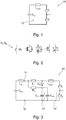
- Fig. 1 is a voltage-driven two-point converter 10 is shown schematically, comprising a Kommut réellesschleife 12 between two semiconductor switches S 1 , S 2 , in which a capacitor C dc is arranged.
- This loop 12 has a leakage inductance or commutation impedance L com .
- the semiconductor switches S 1 , S 2 may comprise, for example, a transistor, thyristor, IGBT, IGCT, RC-IGBT, RC-IGCT, etc.
- Fig. 3 shows a two-point converter 10, which includes further switching components to prevent or at least reduce voltage spikes generated by the leakage inductance L com .
- circuit is a so-called RCLD-damping circuit.
- the components of the converter except the cell capacitor C dc are combined in a common module / stack, wherein the cell capacitor C dc can be connected via terminals 14 and 16 to the module / stack.
- a snubber capacitor C cl1 can be connected in parallel to the cell capacitor C dc and parallel to the series-connected semiconductor switches S 1 , S 2 , which is in spatial proximity to the two semiconductor switches S 1 , S 2 .
- the commutation loop 12 is reduced in size and the inductance of the lines is reduced or the inductance Ls is coupled out of the commutation loop 12.
- a snubber diode D cl and a snubber resistor Rs may be inserted in the commutation loop 12.
- di / dt When the turn-off current or its temporal change is to be controlled di / dt, (for example, between the diode D cl and the semiconductor switches S 1 , S 2 ) and / or if at least a portion of the switching losses of the semiconductor switches S 1 , S 2 in the snubber Resistor Rs is to be performed (for example, for IGBTs as a semiconductor switch S 1 , S 2 ), a di / dt inductor inductance L i can be introduced. The inductance L i can be inserted between the cell capacitor C dc and one of the semiconductor switches S 1 , S 2 .
- one end of the resistor Rs may be connected between the cell capacitor and the inductance L i and / or one end of the diode D cl may be connected between the inductance L i and the semiconductor switch S 1 , S 2 .
- resistor Rs the inductance L i and the diode D cl are not connected to the terminal 14 but to the other terminal 16.
- a snubber capacitor not only a snubber capacitor but a plurality of snubber capacitors C cl1 , C c12 connected in parallel may be used, forming a plurality of commutation loops 12, 12 '.
- the two semiconductor switches S 1 , S 2 and the diode D cl can be arranged together in a stack 18.
- a cooling element 20 or cooling plate 20 is disposed between two semiconductor devices S 1 , S 2 .
- the stack may have a frame 22, with which the components S 1 , S 2 , D cl and 20 can be pressed together. This creates a so-called press pack.
- the diode D cl can also be arranged in an additional stack 24.
- the stack 18 then comprises only the semiconductor switches S 1 , S 2 and the cooling elements 20.
- the stack 18 can be connected to the capacitors C cl1 and C cl2 as well as to the other elements Rs, L i by means of cables, lines and / or bus bars.
- capacitors C cl1 and C c12 and optionally the other components Rs, L i are mechanically connected to the stack 18 and in particular its frame 18.
- capacitors C cl1 and C c12 arranged on the sides of the stack 18 form two parallel commutation loops 12, 12 '.
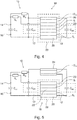
- the Fig. 6 shows a circuit diagram for in the Fig. 7 shown press pack or stack 18, the two series-connected half-bridges 10, 10 'and two-phase converter 10, 10' comprises.
- the semiconductor switches S 1 , S 2 , S 3 and S 4 RC-IGCTs can also be RC-IGBTs or IGBT or IGCT with diodes.
- the semiconductor switches S 1 , S 2 , S 3 and S 4 are connected in series. Also, in the inverter 10, the diode D cl , the inductor L i and the resistor Rs are connected to the upper, first terminal 14, while in the inverter 10 ', these components are connected to the lower second terminal 16. in particular, no additional insulation between the converters 10 and 10 'is necessary.
- the converters 10 and 10 ' can share a heat sink 20 and a cooling box 20, respectively.
- the snubber diode D cl is connected to the semiconductor stack 18 and a mounting bracket 26, respectively.
- the electrically conductive cooling element 20 between the snubber diode D cl and the semiconductor switch S 1 is connected via a conductive connection 28 to an upper, first snubber bus bar 34.
- four snubber capacitors C cl1 , C c12 , C cl1 ', C c12 ' are arranged laterally next to the stack 18 and are connected at an upper end to the first snubber bus bar 34.
- the capacitors C cl1 , C cl1 ' are arranged on one side and the capacitors C c12 , C cl2 ' on the opposite side of the stack 18.
- the capacitors C cl1 , C cl1 ' are connected to a first middle snubber bus bar 36 and the capacitors C c12 , C c12 ' are connected to a second middle bus bar 38.
- the two bus bars 36, 38 are symmetrical to each other and each have a U-shaped bent sheet metal. With the middle part, the two bus bars are connected to an electrically conductive cooling element 20 between the semiconductor switches S 2 and S 4 .
- a lower, second snubber bus bar 40 is connected to the diode D cl of the second inverter 10 '.
- the capacitors C cl1 , C c12 , C cl1 ', C c12 ' of the lower inverter 10 ' are with this diode D cl connected via a bus bar 40 and arranged according to the upper capacitors and connected to the middle busbars 36, 38 accordingly.
Landscapes
- Engineering & Computer Science (AREA)
- Power Engineering (AREA)
- Inverter Devices (AREA)
- Power Conversion In General (AREA)
- Dc-Dc Converters (AREA)
Claims (9)
- Empilement de semi-conducteurs (18) destiné à un convertisseur (10), l'empilement de semi-conducteurs (18) comprenant :deux commutateurs à semi-conducteurs (S1, S2) connectés en série ;deux bornes (14, 16) destinées à raccorder un condensateur à cellule (Cdc), qui sont connectées l'une à l'autre par les deux commutateurs à semi-conducteurs (S1, S2) ;au moins un élément de refroidissement (20) disposé entre les commutateurs à semi-conducteurs (S1, S2) ;un châssis (22) au moyen duquel les commutateurs à semi-conducteurs (S1, S2) et éléments de refroidissement (20) sont fixés les uns aux autres et qui fournit les bornes ; etau moins deux condensateurs d'amortissement (Ccl1, Ccl2) fixés mécaniquement au châssis (22), qui sont connectés en parallèle, sont reliés aux bornes et forment respectivement avec les deux commutateurs à semi-conducteurs (S1, S2) une boucle de commutation (12, 12').
- Empilement de semi-conducteurs (18) selon la revendication 1, comprenant en outre :au moins quatre condensateurs d'amortissement (Ccl1, Ccl2, Ccl1', Ccl2') fixés mécaniquement au châssis (22).
- Empilement de semi-conducteurs (18) selon la revendication 1 ou 2,
dans lequel deux condensateurs d'amortissement (Ccl1, Ccl2) sont disposés sur des côtés opposés de l'empilement de semi-conducteurs. - Empilement de semi-conducteurs (18) selon l'une quelconque des revendications précédentes,
dans lequel deux condensateurs d'amortissement (Ccl1, Ccl1') sont disposés spatialement côte à côte sur un côté de l'empilement de semi-conducteurs. - Empilement de semi-conducteurs (18) selon l'une quelconque des revendications précédentes,
dans lequel les condensateurs d'amortissement (Ccl1, Ccl2, Ccl1', Ccl2') sont réalisés de manière à être du même type. - Empilement de semi-conducteurs (18) selon l'une quelconque des revendications précédentes,
comprenant en outre :une diode d'amortissement (Dcl) ; et/ouune résistance d'amortissement (RS) et/ou une inductance d'arrêt (Li). - Empilement de semi-conducteurs (18) selon l'une quelconque des revendications précédentes, comprenant en outre :une première paire (S1, S2) et une deuxième paire (S3, S4) de commutateurs à semi-conducteurs connectés en série, qui peuvent respectivement être reliées par paires à deux condensateurs à cellules (Cdc) ;au moins deux premiers condensateurs d'amortissement (Ccl1, Ccl2, Ccl1', Ccl2') fixés mécaniquement au châssis (22), qui sont connectés en parallèle et qui forment respectivement une boucle de commutation avec la première paire (S1, S2) de commutateurs à semi-conducteurs ; etau moins deux deuxièmes condensateurs d'amortissement (Ccl1, Ccl2, Ccl1', Ccl2') fixés mécaniquement au châssis (22), qui sont connectés en série et qui forment respectivement une boucle de commutation avec la deuxième paire (S3, S4) de commutateurs à semi-conducteurs.
- Empilement de semi-conducteurs (18) selon l'une quelconque des revendications 7,
dans lequel les premiers condensateurs d'amortissement (Ccl1, Ccl2, Ccl1', Ccl2') sont reliés les uns aux autres par l'intermédiaire d'une première barre omnibus (34), les deuxièmes condensateurs d'amortissement (Ccl1, Ccl2, Ccl1', Ccl2') sont reliés les uns aux autres par l'intermédiaire d'une deuxième barre omnibus (40) et les premiers condensateurs d'amortissement sont reliés les uns aux autres et aux deuxièmes condensateurs d'amortissement par l'intermédiaire d'une barre omnibus (36, 38), dans lequel la barre omnibus (36, 38) est fixée à un corps de refroidissement (20) entre les paires de commutateurs à semi-conducteurs. - Empilement de semi-conducteurs (18) selon l'une quelconque des revendications précédentes,
dans lequel les commutateurs à semi-conducteurs (S1, S2, S3, S4) sont sélectionnés parmi : des transistors, des thyristors, des IGBT, des IGCT, des RC-IGBT et/ou des RC-IGCT.
Applications Claiming Priority (2)
| Application Number | Priority Date | Filing Date | Title |
|---|---|---|---|
| DE202013104510U DE202013104510U1 (de) | 2013-10-04 | 2013-10-04 | Halbleiterstapel für Umrichter mit Snubber-Kondensatoren |
| PCT/EP2014/071296 WO2015049387A1 (fr) | 2013-10-04 | 2014-10-06 | Empilement de semi-conducteurs pour convertisseur équipé de condensateurs d'amortissement |
Publications (2)
| Publication Number | Publication Date |
|---|---|
| EP2989660A1 EP2989660A1 (fr) | 2016-03-02 |
| EP2989660B1 true EP2989660B1 (fr) | 2017-01-04 |
Family
ID=49781040
Family Applications (1)
| Application Number | Title | Priority Date | Filing Date |
|---|---|---|---|
| EP14780861.2A Active EP2989660B1 (fr) | 2013-10-04 | 2014-10-06 | Empilement de semi-conducteurs pour convertisseur équipé de condensateurs d'amortissement |
Country Status (9)
| Country | Link |
|---|---|
| US (1) | US10164519B2 (fr) |
| EP (1) | EP2989660B1 (fr) |
| CN (1) | CN105593989B (fr) |
| AU (1) | AU2014331067A1 (fr) |
| BR (1) | BR112016006798A2 (fr) |
| CA (1) | CA2926022A1 (fr) |
| DE (1) | DE202013104510U1 (fr) |
| MX (1) | MX2016004075A (fr) |
| WO (1) | WO2015049387A1 (fr) |
Families Citing this family (7)
| Publication number | Priority date | Publication date | Assignee | Title |
|---|---|---|---|---|
| DE102014209690B4 (de) * | 2014-05-21 | 2020-02-20 | Robert Bosch Gmbh | Kommutierungszelle |
| FR3043284B1 (fr) * | 2015-10-29 | 2023-06-23 | Ifp Energies Now | Systeme de conversion d'une puissance electrique continue en puissance electrique alternative avec module recuperateur d'energie |
| WO2018006970A1 (fr) * | 2016-07-07 | 2018-01-11 | Abb Schweiz Ag | Pile d'énergie à semi-conducteur d'un convertisseur modulaire multiniveaux |
| DE102017203420A1 (de) * | 2017-03-02 | 2018-09-06 | Siemens Aktiengesellschaft | Halbbrücke für leistungselektronische Schaltungen |
| KR102661064B1 (ko) * | 2019-10-15 | 2024-04-26 | 히타치 에너지 리미티드 | 스너버 컴포넌트들을 갖는 스위칭 회로 |
| EP4429098A1 (fr) * | 2023-03-10 | 2024-09-11 | GE Energy Power Conversion Technology Ltd | Sous-module et module, tour, convertisseur de puissance et système d'alimentation associés |
| CN120165582A (zh) * | 2023-12-15 | 2025-06-17 | 宁德时代未来能源(上海)研究院有限公司 | 阀组件、功率模块、储能子模块及储能系统 |
Family Cites Families (26)
| Publication number | Priority date | Publication date | Assignee | Title |
|---|---|---|---|---|
| JPS589349A (ja) * | 1981-07-10 | 1983-01-19 | Hitachi Ltd | Gtoスタツク |
| US4674024A (en) * | 1986-06-05 | 1987-06-16 | Westinghouse Electric Corp. | High voltage modular inverter and control system thereof |
| FI880817L (fi) * | 1987-07-17 | 1989-01-18 | Siemens Ag | Anordning foer koppling med laog foerlust av ett halvledarkopplingselement i en trepunktvaexelriktare. |
| DE3743436C1 (de) * | 1987-12-21 | 1989-05-11 | Siemens Ag | Schaltentlasteter,verlustarmer Dreipunktwechselrichter |
| US5045924A (en) * | 1988-02-26 | 1991-09-03 | Kabushiki Kaisha Toshiba | Mounting structure of semiconductor converter |
| JP2658427B2 (ja) * | 1989-01-17 | 1997-09-30 | 富士電機株式会社 | 電力変換用半導体素子のスナバ回路とそのモジュール装置 |
| JP3325030B2 (ja) * | 1991-06-06 | 2002-09-17 | 三菱電機株式会社 | 3レベルインバータ装置 |
| EP0838855B1 (fr) | 1991-09-20 | 2004-11-24 | Hitachi, Ltd. | Module semi-conducteur |
| JP3173068B2 (ja) * | 1991-10-22 | 2001-06-04 | 株式会社日立製作所 | 電力変換器 |
| JP2735497B2 (ja) * | 1995-01-31 | 1998-04-02 | 株式会社東芝 | スナバ回路 |
| DE19523095A1 (de) * | 1995-06-26 | 1997-01-02 | Abb Management Ag | Stromrichterschaltungsanordnung |
| US6169672B1 (en) * | 1996-07-03 | 2001-01-02 | Hitachi, Ltd. | Power converter with clamping circuit |
| DE19632173A1 (de) * | 1996-08-09 | 1998-02-12 | Asea Brown Boveri | Stromrichterschaltungsanordnung |
| US5982646A (en) * | 1998-06-30 | 1999-11-09 | General Electric Company | Voltage clamp snubbers for three level converter |
| JP2001057407A (ja) | 1999-08-19 | 2001-02-27 | Meidensha Corp | ヒートシンク配置装置 |
| JP3652934B2 (ja) * | 1999-09-06 | 2005-05-25 | 東芝三菱電機産業システム株式会社 | 電力変換装置 |
| DE10062075A1 (de) * | 2000-12-13 | 2002-06-27 | Bosch Gmbh Robert | Umrichter mit integrierten Zwischenkreiskondensatoren |
| WO2003017452A2 (fr) * | 2001-08-13 | 2003-02-27 | Inductotherm Corp. | Circuit d'alimentation en puissance tolerant un courant de defaut |
| US20080043500A1 (en) * | 2004-07-01 | 2008-02-21 | Katsunori Asano | Snubber Circuit and Power Semiconductor Device Having Snubber Circuit |
| JP4661645B2 (ja) | 2005-03-23 | 2011-03-30 | トヨタ自動車株式会社 | パワー半導体モジュール |
| CA2718935C (fr) * | 2008-03-20 | 2016-05-10 | Abb Technology Ag | Convertisseur de source de tension |
| US8385068B2 (en) * | 2009-06-16 | 2013-02-26 | Abb Technology Ag | Cooling of electrical components |
| JP5218541B2 (ja) | 2010-12-14 | 2013-06-26 | 株式会社デンソー | スイッチングモジュール |
| FR2976404B1 (fr) * | 2011-06-10 | 2013-07-12 | Converteam Technology Ltd | Pile de composants electroniques maintenus suivant un empilement presse |
| WO2013009711A1 (fr) * | 2011-07-08 | 2013-01-17 | Timler John P | Isolateur basé sur une ou plusieurs structures diélectriques |
| DE202012008739U1 (de) | 2012-09-12 | 2013-12-16 | Abb Technology Ag | Kühlkreislauf mit ausreichend knapp bemessenem Wärmetauscher |
-
2013
- 2013-10-04 DE DE202013104510U patent/DE202013104510U1/de not_active Expired - Lifetime
-
2014
- 2014-10-06 AU AU2014331067A patent/AU2014331067A1/en not_active Abandoned
- 2014-10-06 WO PCT/EP2014/071296 patent/WO2015049387A1/fr not_active Ceased
- 2014-10-06 BR BR112016006798A patent/BR112016006798A2/pt not_active IP Right Cessation
- 2014-10-06 EP EP14780861.2A patent/EP2989660B1/fr active Active
- 2014-10-06 CN CN201480054633.9A patent/CN105593989B/zh active Active
- 2014-10-06 CA CA2926022A patent/CA2926022A1/fr not_active Abandoned
- 2014-10-06 MX MX2016004075A patent/MX2016004075A/es unknown
-
2016
- 2016-04-01 US US15/088,812 patent/US10164519B2/en active Active
Also Published As
| Publication number | Publication date |
|---|---|
| US10164519B2 (en) | 2018-12-25 |
| CN105593989B (zh) | 2019-12-24 |
| CA2926022A1 (fr) | 2015-04-09 |
| US20160218615A1 (en) | 2016-07-28 |
| EP2989660A1 (fr) | 2016-03-02 |
| AU2014331067A1 (en) | 2016-05-05 |
| DE202013104510U1 (de) | 2013-11-14 |
| WO2015049387A1 (fr) | 2015-04-09 |
| CN105593989A (zh) | 2016-05-18 |
| MX2016004075A (es) | 2016-08-11 |
| BR112016006798A2 (pt) | 2017-08-01 |
Similar Documents
| Publication | Publication Date | Title |
|---|---|---|
| DE19732402B4 (de) | Elektrische Busanordnung zur Gleichstromversorgung von Schaltungselementen eines Wechselrichters | |
| EP2989660A1 (fr) | Empilement de semi-conducteurs pour convertisseur équipé de condensateurs d'amortissement | |
| DE102018106357A1 (de) | Leistungsumwandlungsgerät | |
| EP2996449B1 (fr) | Système de convertisseur de courant doté d'un convertisseur multiphases | |
| DE102010002627A1 (de) | Niederinduktive Leistungshalbleiterbaugruppe | |
| DE4110339A1 (de) | Wechselrichtereinheit mit verbesserter stromleiterplattenkonfiguration | |
| WO2017174102A1 (fr) | Module pour convertisseur à plusieurs niveaux | |
| WO2011086048A9 (fr) | Circuit de disjoncteurs électroniques d'un générateur de courant | |
| EP3404818B1 (fr) | Dispositif de semi-conducteurs | |
| EP3180850B1 (fr) | Circuit faiblement inductif d'un convertisseur | |
| DE102018200712A1 (de) | Wandlervorrichtung elektrischer Leistung, Solarenergie-Aufbereitungssystem, Stromspeichersystem, unterbrechungsfreies Leistungsversorgungssystem, Windenergieerzeugungssystem und Motorantriebssystem | |
| DE102013104522B3 (de) | Leistungshalbleitermodul mit Subeinheiten und Anordnung hiermit | |
| DE202015004662U1 (de) | Zwischenkreiskondensatormodul mit niederinduktiven Busbar-Verbindungen | |
| DE102004059313B3 (de) | Leistungshalbleitermodul mit verringerten parasitären Induktivitäten | |
| EP3098958B1 (fr) | Disposition de convertisseurs à couplage capacitif | |
| EP2564501B1 (fr) | Sous-module destiné à un convertisseur modulaire à étages multiples | |
| EP3571758B1 (fr) | Onduleur modulaire | |
| DE19523095A1 (de) | Stromrichterschaltungsanordnung | |
| WO2001039347A1 (fr) | Dispositif de protection contre les surtensions, provoquees par des commutations, aux bornes d'un equipement electrique | |
| EP3304718B1 (fr) | Convertisseur continu-continu pour hautes tensions | |
| DE102014111438B4 (de) | Leistungsbaustein und Verfahren zu dessen Herstellung | |
| DE102013102707A1 (de) | Wechselrichter mit mindestens einer Wechselrichterbrücke zwischen zwei Busbars | |
| WO2018113926A1 (fr) | Convertisseur | |
| EP4285482B1 (fr) | Cellule de commutation, module de condensateur volant et onduleur à niveaux multiples | |
| WO2002069482A1 (fr) | Conception d'un circuit servant à la commutation de courants |
Legal Events
| Date | Code | Title | Description |
|---|---|---|---|
| PUAI | Public reference made under article 153(3) epc to a published international application that has entered the european phase |
Free format text: ORIGINAL CODE: 0009012 |
|
| 17P | Request for examination filed |
Effective date: 20151127 |
|
| AK | Designated contracting states |
Kind code of ref document: A1 Designated state(s): AL AT BE BG CH CY CZ DE DK EE ES FI FR GB GR HR HU IE IS IT LI LT LU LV MC MK MT NL NO PL PT RO RS SE SI SK SM TR |
|
| AX | Request for extension of the european patent |
Extension state: BA ME |
|
| GRAP | Despatch of communication of intention to grant a patent |
Free format text: ORIGINAL CODE: EPIDOSNIGR1 |
|
| INTG | Intention to grant announced |
Effective date: 20160623 |
|
| GRAS | Grant fee paid |
Free format text: ORIGINAL CODE: EPIDOSNIGR3 |
|
| RAP1 | Party data changed (applicant data changed or rights of an application transferred) |
Owner name: ABB SCHWEIZ AG |
|
| GRAA | (expected) grant |
Free format text: ORIGINAL CODE: 0009210 |
|
| DAX | Request for extension of the european patent (deleted) | ||
| AK | Designated contracting states |
Kind code of ref document: B1 Designated state(s): AL AT BE BG CH CY CZ DE DK EE ES FI FR GB GR HR HU IE IS IT LI LT LU LV MC MK MT NL NO PL PT RO RS SE SI SK SM TR |
|
| REG | Reference to a national code |
Ref country code: GB Ref legal event code: FG4D Free format text: NOT ENGLISH |
|
| REG | Reference to a national code |
Ref country code: CH Ref legal event code: EP |
|
| REG | Reference to a national code |
Ref country code: AT Ref legal event code: REF Ref document number: 860001 Country of ref document: AT Kind code of ref document: T Effective date: 20170115 |
|
| REG | Reference to a national code |
Ref country code: IE Ref legal event code: FG4D Free format text: LANGUAGE OF EP DOCUMENT: GERMAN |
|
| REG | Reference to a national code |
Ref country code: DE Ref legal event code: R096 Ref document number: 502014002422 Country of ref document: DE |
|
| REG | Reference to a national code |
Ref country code: LT Ref legal event code: MG4D Ref country code: NL Ref legal event code: MP Effective date: 20170104 |
|
| PG25 | Lapsed in a contracting state [announced via postgrant information from national office to epo] |
Ref country code: NL Free format text: LAPSE BECAUSE OF FAILURE TO SUBMIT A TRANSLATION OF THE DESCRIPTION OR TO PAY THE FEE WITHIN THE PRESCRIBED TIME-LIMIT Effective date: 20170104 |
|
| PG25 | Lapsed in a contracting state [announced via postgrant information from national office to epo] |
Ref country code: FI Free format text: LAPSE BECAUSE OF FAILURE TO SUBMIT A TRANSLATION OF THE DESCRIPTION OR TO PAY THE FEE WITHIN THE PRESCRIBED TIME-LIMIT Effective date: 20170104 Ref country code: NO Free format text: LAPSE BECAUSE OF FAILURE TO SUBMIT A TRANSLATION OF THE DESCRIPTION OR TO PAY THE FEE WITHIN THE PRESCRIBED TIME-LIMIT Effective date: 20170404 Ref country code: GR Free format text: LAPSE BECAUSE OF FAILURE TO SUBMIT A TRANSLATION OF THE DESCRIPTION OR TO PAY THE FEE WITHIN THE PRESCRIBED TIME-LIMIT Effective date: 20170405 Ref country code: HR Free format text: LAPSE BECAUSE OF FAILURE TO SUBMIT A TRANSLATION OF THE DESCRIPTION OR TO PAY THE FEE WITHIN THE PRESCRIBED TIME-LIMIT Effective date: 20170104 Ref country code: LT Free format text: LAPSE BECAUSE OF FAILURE TO SUBMIT A TRANSLATION OF THE DESCRIPTION OR TO PAY THE FEE WITHIN THE PRESCRIBED TIME-LIMIT Effective date: 20170104 Ref country code: IS Free format text: LAPSE BECAUSE OF FAILURE TO SUBMIT A TRANSLATION OF THE DESCRIPTION OR TO PAY THE FEE WITHIN THE PRESCRIBED TIME-LIMIT Effective date: 20170504 |
|
| PG25 | Lapsed in a contracting state [announced via postgrant information from national office to epo] |
Ref country code: LV Free format text: LAPSE BECAUSE OF FAILURE TO SUBMIT A TRANSLATION OF THE DESCRIPTION OR TO PAY THE FEE WITHIN THE PRESCRIBED TIME-LIMIT Effective date: 20170104 Ref country code: BG Free format text: LAPSE BECAUSE OF FAILURE TO SUBMIT A TRANSLATION OF THE DESCRIPTION OR TO PAY THE FEE WITHIN THE PRESCRIBED TIME-LIMIT Effective date: 20170404 Ref country code: PL Free format text: LAPSE BECAUSE OF FAILURE TO SUBMIT A TRANSLATION OF THE DESCRIPTION OR TO PAY THE FEE WITHIN THE PRESCRIBED TIME-LIMIT Effective date: 20170104 Ref country code: RS Free format text: LAPSE BECAUSE OF FAILURE TO SUBMIT A TRANSLATION OF THE DESCRIPTION OR TO PAY THE FEE WITHIN THE PRESCRIBED TIME-LIMIT Effective date: 20170104 Ref country code: PT Free format text: LAPSE BECAUSE OF FAILURE TO SUBMIT A TRANSLATION OF THE DESCRIPTION OR TO PAY THE FEE WITHIN THE PRESCRIBED TIME-LIMIT Effective date: 20170504 Ref country code: SE Free format text: LAPSE BECAUSE OF FAILURE TO SUBMIT A TRANSLATION OF THE DESCRIPTION OR TO PAY THE FEE WITHIN THE PRESCRIBED TIME-LIMIT Effective date: 20170104 Ref country code: ES Free format text: LAPSE BECAUSE OF FAILURE TO SUBMIT A TRANSLATION OF THE DESCRIPTION OR TO PAY THE FEE WITHIN THE PRESCRIBED TIME-LIMIT Effective date: 20170104 |
|
| REG | Reference to a national code |
Ref country code: DE Ref legal event code: R097 Ref document number: 502014002422 Country of ref document: DE |
|
| REG | Reference to a national code |
Ref country code: FR Ref legal event code: PLFP Year of fee payment: 4 |
|
| PG25 | Lapsed in a contracting state [announced via postgrant information from national office to epo] |
Ref country code: IT Free format text: LAPSE BECAUSE OF FAILURE TO SUBMIT A TRANSLATION OF THE DESCRIPTION OR TO PAY THE FEE WITHIN THE PRESCRIBED TIME-LIMIT Effective date: 20170104 Ref country code: EE Free format text: LAPSE BECAUSE OF FAILURE TO SUBMIT A TRANSLATION OF THE DESCRIPTION OR TO PAY THE FEE WITHIN THE PRESCRIBED TIME-LIMIT Effective date: 20170104 Ref country code: SK Free format text: LAPSE BECAUSE OF FAILURE TO SUBMIT A TRANSLATION OF THE DESCRIPTION OR TO PAY THE FEE WITHIN THE PRESCRIBED TIME-LIMIT Effective date: 20170104 Ref country code: RO Free format text: LAPSE BECAUSE OF FAILURE TO SUBMIT A TRANSLATION OF THE DESCRIPTION OR TO PAY THE FEE WITHIN THE PRESCRIBED TIME-LIMIT Effective date: 20170104 Ref country code: CZ Free format text: LAPSE BECAUSE OF FAILURE TO SUBMIT A TRANSLATION OF THE DESCRIPTION OR TO PAY THE FEE WITHIN THE PRESCRIBED TIME-LIMIT Effective date: 20170104 |
|
| PLBE | No opposition filed within time limit |
Free format text: ORIGINAL CODE: 0009261 |
|
| STAA | Information on the status of an ep patent application or granted ep patent |
Free format text: STATUS: NO OPPOSITION FILED WITHIN TIME LIMIT |
|
| PG25 | Lapsed in a contracting state [announced via postgrant information from national office to epo] |
Ref country code: DK Free format text: LAPSE BECAUSE OF FAILURE TO SUBMIT A TRANSLATION OF THE DESCRIPTION OR TO PAY THE FEE WITHIN THE PRESCRIBED TIME-LIMIT Effective date: 20170104 Ref country code: SM Free format text: LAPSE BECAUSE OF FAILURE TO SUBMIT A TRANSLATION OF THE DESCRIPTION OR TO PAY THE FEE WITHIN THE PRESCRIBED TIME-LIMIT Effective date: 20170104 |
|
| PG25 | Lapsed in a contracting state [announced via postgrant information from national office to epo] |
Ref country code: SI Free format text: LAPSE BECAUSE OF FAILURE TO SUBMIT A TRANSLATION OF THE DESCRIPTION OR TO PAY THE FEE WITHIN THE PRESCRIBED TIME-LIMIT Effective date: 20170104 |
|
| PG25 | Lapsed in a contracting state [announced via postgrant information from national office to epo] |
Ref country code: MC Free format text: LAPSE BECAUSE OF FAILURE TO SUBMIT A TRANSLATION OF THE DESCRIPTION OR TO PAY THE FEE WITHIN THE PRESCRIBED TIME-LIMIT Effective date: 20170104 |
|
| REG | Reference to a national code |
Ref country code: IE Ref legal event code: MM4A |
|
| PG25 | Lapsed in a contracting state [announced via postgrant information from national office to epo] |
Ref country code: LU Free format text: LAPSE BECAUSE OF NON-PAYMENT OF DUE FEES Effective date: 20171006 |
|
| REG | Reference to a national code |
Ref country code: BE Ref legal event code: MM Effective date: 20171031 |
|
| PG25 | Lapsed in a contracting state [announced via postgrant information from national office to epo] |
Ref country code: BE Free format text: LAPSE BECAUSE OF NON-PAYMENT OF DUE FEES Effective date: 20171031 |
|
| PG25 | Lapsed in a contracting state [announced via postgrant information from national office to epo] |
Ref country code: MT Free format text: LAPSE BECAUSE OF FAILURE TO SUBMIT A TRANSLATION OF THE DESCRIPTION OR TO PAY THE FEE WITHIN THE PRESCRIBED TIME-LIMIT Effective date: 20170104 |
|
| REG | Reference to a national code |
Ref country code: FR Ref legal event code: PLFP Year of fee payment: 5 |
|
| PG25 | Lapsed in a contracting state [announced via postgrant information from national office to epo] |
Ref country code: IE Free format text: LAPSE BECAUSE OF NON-PAYMENT OF DUE FEES Effective date: 20171006 |
|
| PG25 | Lapsed in a contracting state [announced via postgrant information from national office to epo] |
Ref country code: HU Free format text: LAPSE BECAUSE OF FAILURE TO SUBMIT A TRANSLATION OF THE DESCRIPTION OR TO PAY THE FEE WITHIN THE PRESCRIBED TIME-LIMIT; INVALID AB INITIO Effective date: 20141006 |
|
| PG25 | Lapsed in a contracting state [announced via postgrant information from national office to epo] |
Ref country code: CY Free format text: LAPSE BECAUSE OF FAILURE TO SUBMIT A TRANSLATION OF THE DESCRIPTION OR TO PAY THE FEE WITHIN THE PRESCRIBED TIME-LIMIT Effective date: 20170104 |
|
| PG25 | Lapsed in a contracting state [announced via postgrant information from national office to epo] |
Ref country code: MK Free format text: LAPSE BECAUSE OF FAILURE TO SUBMIT A TRANSLATION OF THE DESCRIPTION OR TO PAY THE FEE WITHIN THE PRESCRIBED TIME-LIMIT Effective date: 20170104 |
|
| PG25 | Lapsed in a contracting state [announced via postgrant information from national office to epo] |
Ref country code: TR Free format text: LAPSE BECAUSE OF FAILURE TO SUBMIT A TRANSLATION OF THE DESCRIPTION OR TO PAY THE FEE WITHIN THE PRESCRIBED TIME-LIMIT Effective date: 20170104 |
|
| PG25 | Lapsed in a contracting state [announced via postgrant information from national office to epo] |
Ref country code: AL Free format text: LAPSE BECAUSE OF FAILURE TO SUBMIT A TRANSLATION OF THE DESCRIPTION OR TO PAY THE FEE WITHIN THE PRESCRIBED TIME-LIMIT Effective date: 20170104 |
|
| REG | Reference to a national code |
Ref country code: CH Ref legal event code: NV Representative=s name: DENNEMEYER AG, CH Ref country code: CH Ref legal event code: PUE Owner name: ABB POWER GRIDS SWITZERLAND AG, CH Free format text: FORMER OWNER: ABB SCHWEIZ AG, CH |
|
| REG | Reference to a national code |
Ref country code: DE Ref legal event code: R081 Ref document number: 502014002422 Country of ref document: DE Owner name: HITACHI ENERGY SWITZERLAND AG, CH Free format text: FORMER OWNER: ABB SCHWEIZ AG, BADEN, CH Ref country code: DE Ref legal event code: R082 Ref document number: 502014002422 Country of ref document: DE Representative=s name: DENNEMEYER & ASSOCIATES RECHTSANWALTSGESELLSCH, DE Ref country code: DE Ref legal event code: R081 Ref document number: 502014002422 Country of ref document: DE Owner name: HITACHI ENERGY LTD, CH Free format text: FORMER OWNER: ABB SCHWEIZ AG, BADEN, CH Ref country code: DE Ref legal event code: R082 Ref document number: 502014002422 Country of ref document: DE Representative=s name: DENNEMEYER & ASSOCIATES S.A., DE Ref country code: DE Ref legal event code: R081 Ref document number: 502014002422 Country of ref document: DE Owner name: ABB POWER GRIDS SWITZERLAND AG, CH Free format text: FORMER OWNER: ABB SCHWEIZ AG, BADEN, CH |
|
| REG | Reference to a national code |
Ref country code: AT Ref legal event code: PC Ref document number: 860001 Country of ref document: AT Kind code of ref document: T Owner name: ABB POWER GRIDS SWITZERLAND AG, CH Effective date: 20210708 |
|
| REG | Reference to a national code |
Ref country code: GB Ref legal event code: 732E Free format text: REGISTERED BETWEEN 20220421 AND 20220427 |
|
| REG | Reference to a national code |
Ref country code: DE Ref legal event code: R081 Ref document number: 502014002422 Country of ref document: DE Owner name: HITACHI ENERGY SWITZERLAND AG, CH Free format text: FORMER OWNER: ABB POWER GRIDS SWITZERLAND AG, BADEN, CH Ref country code: DE Ref legal event code: R081 Ref document number: 502014002422 Country of ref document: DE Owner name: HITACHI ENERGY LTD, CH Free format text: FORMER OWNER: ABB POWER GRIDS SWITZERLAND AG, BADEN, CH |
|
| REG | Reference to a national code |
Ref country code: AT Ref legal event code: HC Ref document number: 860001 Country of ref document: AT Kind code of ref document: T Owner name: HITACHI ENERGY SWITZERLAND AG, CH Effective date: 20220718 |
|
| P01 | Opt-out of the competence of the unified patent court (upc) registered |
Effective date: 20230527 |
|
| REG | Reference to a national code |
Ref country code: DE Ref legal event code: R082 Ref document number: 502014002422 Country of ref document: DE Representative=s name: DENNEMEYER & ASSOCIATES RECHTSANWALTSGESELLSCH, DE Ref country code: DE Ref legal event code: R082 Ref document number: 502014002422 Country of ref document: DE Representative=s name: DENNEMEYER & ASSOCIATES S.A., DE Ref country code: DE Ref legal event code: R081 Ref document number: 502014002422 Country of ref document: DE Owner name: HITACHI ENERGY LTD, CH Free format text: FORMER OWNER: HITACHI ENERGY SWITZERLAND AG, BADEN, CH |
|
| REG | Reference to a national code |
Ref country code: AT Ref legal event code: PC Ref document number: 860001 Country of ref document: AT Kind code of ref document: T Owner name: HITACHI ENERGY LTD, CH Effective date: 20240416 |
|
| REG | Reference to a national code |
Ref country code: GB Ref legal event code: 732E Free format text: REGISTERED BETWEEN 20240718 AND 20240724 |
|
| REG | Reference to a national code |
Ref country code: DE Ref legal event code: R079 Ref document number: 502014002422 Country of ref document: DE Free format text: PREVIOUS MAIN CLASS: H01L0025070000 Ipc: H10D0080200000 |
|
| REG | Reference to a national code |
Ref country code: DE Ref legal event code: R082 Ref document number: 502014002422 Country of ref document: DE Representative=s name: DENNEMEYER & ASSOCIATES RECHTSANWALTSGESELLSCH, DE |
|
| REG | Reference to a national code |
Ref country code: CH Ref legal event code: U11 Free format text: ST27 STATUS EVENT CODE: U-0-0-U10-U11 (AS PROVIDED BY THE NATIONAL OFFICE) Effective date: 20251101 |
|
| PGFP | Annual fee paid to national office [announced via postgrant information from national office to epo] |
Ref country code: DE Payment date: 20251021 Year of fee payment: 12 |
|
| PGFP | Annual fee paid to national office [announced via postgrant information from national office to epo] |
Ref country code: GB Payment date: 20251022 Year of fee payment: 12 |
|
| PGFP | Annual fee paid to national office [announced via postgrant information from national office to epo] |
Ref country code: AT Payment date: 20251022 Year of fee payment: 12 |
|
| PGFP | Annual fee paid to national office [announced via postgrant information from national office to epo] |
Ref country code: FR Payment date: 20251030 Year of fee payment: 12 |
|
| PGFP | Annual fee paid to national office [announced via postgrant information from national office to epo] |
Ref country code: CH Payment date: 20251101 Year of fee payment: 12 |