EP2993253A1 - Elektronische komponente - Google Patents
Elektronische komponente Download PDFInfo
- Publication number
- EP2993253A1 EP2993253A1 EP14791907.0A EP14791907A EP2993253A1 EP 2993253 A1 EP2993253 A1 EP 2993253A1 EP 14791907 A EP14791907 A EP 14791907A EP 2993253 A1 EP2993253 A1 EP 2993253A1
- Authority
- EP
- European Patent Office
- Prior art keywords
- plating layer
- sample
- test
- corrosion
- contact
- Prior art date
- Legal status (The legal status is an assumption and is not a legal conclusion. Google has not performed a legal analysis and makes no representation as to the accuracy of the status listed.)
- Granted
Links
Images




Classifications
-
- C—CHEMISTRY; METALLURGY
- C25—ELECTROLYTIC OR ELECTROPHORETIC PROCESSES; APPARATUS THEREFOR
- C25D—PROCESSES FOR THE ELECTROLYTIC OR ELECTROPHORETIC PRODUCTION OF COATINGS; ELECTROFORMING; APPARATUS THEREFOR
- C25D5/00—Electroplating characterised by the process; Pretreatment or after-treatment of workpieces
- C25D5/60—Electroplating characterised by the structure or texture of the layers
- C25D5/615—Microstructure of the layers, e.g. mixed structure
- C25D5/619—Amorphous layers
-
- C—CHEMISTRY; METALLURGY
- C25—ELECTROLYTIC OR ELECTROPHORETIC PROCESSES; APPARATUS THEREFOR
- C25D—PROCESSES FOR THE ELECTROLYTIC OR ELECTROPHORETIC PRODUCTION OF COATINGS; ELECTROFORMING; APPARATUS THEREFOR
- C25D5/00—Electroplating characterised by the process; Pretreatment or after-treatment of workpieces
- C25D5/10—Electroplating with more than one layer of the same or of different metals
- C25D5/12—Electroplating with more than one layer of the same or of different metals at least one layer being of nickel or chromium
-
- C—CHEMISTRY; METALLURGY
- C25—ELECTROLYTIC OR ELECTROPHORETIC PROCESSES; APPARATUS THEREFOR
- C25D—PROCESSES FOR THE ELECTROLYTIC OR ELECTROPHORETIC PRODUCTION OF COATINGS; ELECTROFORMING; APPARATUS THEREFOR
- C25D5/00—Electroplating characterised by the process; Pretreatment or after-treatment of workpieces
- C25D5/48—After-treatment of electroplated surfaces
-
- C—CHEMISTRY; METALLURGY
- C25—ELECTROLYTIC OR ELECTROPHORETIC PROCESSES; APPARATUS THEREFOR
- C25D—PROCESSES FOR THE ELECTROLYTIC OR ELECTROPHORETIC PRODUCTION OF COATINGS; ELECTROFORMING; APPARATUS THEREFOR
- C25D5/00—Electroplating characterised by the process; Pretreatment or after-treatment of workpieces
- C25D5/60—Electroplating characterised by the structure or texture of the layers
- C25D5/615—Microstructure of the layers, e.g. mixed structure
- C25D5/617—Crystalline layers
-
- C—CHEMISTRY; METALLURGY
- C25—ELECTROLYTIC OR ELECTROPHORETIC PROCESSES; APPARATUS THEREFOR
- C25D—PROCESSES FOR THE ELECTROLYTIC OR ELECTROPHORETIC PRODUCTION OF COATINGS; ELECTROFORMING; APPARATUS THEREFOR
- C25D7/00—Electroplating characterised by the article coated
-
- H—ELECTRICITY
- H01—ELECTRIC ELEMENTS
- H01R—ELECTRICALLY-CONDUCTIVE CONNECTIONS; STRUCTURAL ASSOCIATIONS OF A PLURALITY OF MUTUALLY-INSULATED ELECTRICAL CONNECTING ELEMENTS; COUPLING DEVICES; CURRENT COLLECTORS
- H01R13/00—Details of coupling devices of the kinds covered by groups H01R12/70 or H01R24/00 - H01R33/00
- H01R13/02—Contact members
- H01R13/03—Contact members characterised by the material, e.g. plating, or coating materials
-
- H—ELECTRICITY
- H01—ELECTRIC ELEMENTS
- H01R—ELECTRICALLY-CONDUCTIVE CONNECTIONS; STRUCTURAL ASSOCIATIONS OF A PLURALITY OF MUTUALLY-INSULATED ELECTRICAL CONNECTING ELEMENTS; COUPLING DEVICES; CURRENT COLLECTORS
- H01R13/00—Details of coupling devices of the kinds covered by groups H01R12/70 or H01R24/00 - H01R33/00
- H01R13/02—Contact members
- H01R13/03—Contact members characterised by the material, e.g. plating, or coating materials
- H01R13/035—Plated dielectric material
-
- C—CHEMISTRY; METALLURGY
- C25—ELECTROLYTIC OR ELECTROPHORETIC PROCESSES; APPARATUS THEREFOR
- C25D—PROCESSES FOR THE ELECTROLYTIC OR ELECTROPHORETIC PRODUCTION OF COATINGS; ELECTROFORMING; APPARATUS THEREFOR
- C25D3/00—Electroplating: Baths therefor
- C25D3/02—Electroplating: Baths therefor from solutions
- C25D3/12—Electroplating: Baths therefor from solutions of nickel or cobalt
-
- C—CHEMISTRY; METALLURGY
- C25—ELECTROLYTIC OR ELECTROPHORETIC PROCESSES; APPARATUS THEREFOR
- C25D—PROCESSES FOR THE ELECTROLYTIC OR ELECTROPHORETIC PRODUCTION OF COATINGS; ELECTROFORMING; APPARATUS THEREFOR
- C25D3/00—Electroplating: Baths therefor
- C25D3/02—Electroplating: Baths therefor from solutions
- C25D3/48—Electroplating: Baths therefor from solutions of gold
-
- C—CHEMISTRY; METALLURGY
- C25—ELECTROLYTIC OR ELECTROPHORETIC PROCESSES; APPARATUS THEREFOR
- C25D—PROCESSES FOR THE ELECTROLYTIC OR ELECTROPHORETIC PRODUCTION OF COATINGS; ELECTROFORMING; APPARATUS THEREFOR
- C25D5/00—Electroplating characterised by the process; Pretreatment or after-treatment of workpieces
- C25D5/34—Pretreatment of metallic surfaces to be electroplated
-
- H—ELECTRICITY
- H01—ELECTRIC ELEMENTS
- H01R—ELECTRICALLY-CONDUCTIVE CONNECTIONS; STRUCTURAL ASSOCIATIONS OF A PLURALITY OF MUTUALLY-INSULATED ELECTRICAL CONNECTING ELEMENTS; COUPLING DEVICES; CURRENT COLLECTORS
- H01R24/00—Two-part coupling devices, or either of their cooperating parts, characterised by their overall structure
- H01R24/60—Contacts spaced along planar side wall transverse to longitudinal axis of engagement
- H01R24/62—Sliding engagements with one side only, e.g. modular jack coupling devices
Definitions
- the present invention relates to an electronic component such as a connector, a relay, a switch and a terminal used for electric (electronic) equipment such as portable terminals, laptop computers, audio equipment, and digital cameras, and particularly relates to a technique of improving corrosion resistance of a contact member of electronic components.
- Contact members used for electronic components described above may be made of a base material of copper or a copper alloy such as phosphor bronze or brass and a gold plating applied thereon. Gold plating prevents an oxide film, and has a good contact resistance value stability and a good corrosion resistance.
- Patent Document 1 As described in Patent Document 1 below, the applicant has proposed providing an appropriate plating layer between a conductive base material and a main plating layer formed on the conductive base material to prevent corrosion and to improve connection reliability of a contact member, and, according to this proposal, a good result is obtained in a corrosion resistance test using a three-gas mixture flow (H 2 S, SO 2 , NO 2 ).
- Patent Document 1 WO 2010/005088
- S-ATA Serial Advanced Technology Attachment
- H 2 S, SO 2 , NO 2 , Cl 2 a corrosion resistance test using a four-gas mixture flow
- Patent Document 1 Some of the electronic components described in the aforementioned Patent Document 1 do not comply with the corrosion resistance test by a four-gas mixture flow, and thus a further improvement in corrosion resistance is desired.
- Increasing the thickness of a main plating layer could improve corrosion-resistance, but also has a disadvantage of an increased cost.
- an acidic electrolytic solution is produced by an interaction between a mixed corrosive gas and water, and attaches to an Au plating surface.
- An interior of a test chamber is under a humidity environment of a relative humidity of 70% RH (temperature 35 C°), and thus the acid electrolytic solution is produced by dissolution of the corrosive gas into moisture.
- sulfite ions HSO 3 -
- formulae (I) and (II) indicated below are produced as expressed by formulae (I) and (II) indicated below, and subsequently, react with dissolved oxygen in water as expressed by formula (III) indicated below to produce sulfate ions (SO 4 2- ).
- the Au plating serves as cathodes and Cu atoms elute by a local cell mechanism, and the Cu atoms diffuse and dissolve intensively at those locations.
- the eluted Cu reacts with sulfate ions, hydroxide ions, hydrosulfide ions contained in the electrolytic solution and the test chamber atmosphere, thus locally produce an insoluble corrosion product composed primarily of Cu, such as Cu 4 (SO 4 )(OH) 6 and sulfide (CuS).
- an Au plating grain boundary expands along with production and growth of the Cu-based corrosion product, and thus, including its periphery, the Cu atoms readily diffuse and a spot-like corrosion product is produced. Therefore, a compound composed primarily of Cu including sulfate ions is produced at an initial step of the corrosion.
- diffusion of Ni atoms that are present in the Au plating also accelerate along with growth and expansion of the corrosion product of a Cu compound, and the diffusion of the Ni atoms is accelerated inside and at a surface of the Cu corrosion product where diffusion is easy.
- the Ni atoms are electrochemically under a strong influence of the local cell mechanism, and thus they dissolve at an accelerating rate. In this step, it is presumed that the dissolution reaction of the Cu atoms stops.
- a compound of Ni including sulfate ions is eventually produced, and further, diffusion of the Ni atoms is accelerated (a quantity of ionized Ni atoms is supplied) and these phenomena occurs continuously, a void is formed in the Ni plating layer as shown in FIG. 18 .
- a four-gas mixture test which is a corrosion resistance test standard under S-ATA, was carried out using Au/Ni/Brass and Au/Ni-P/Brass connectors, and the result showed that the undercoat Ni-P alloy plating which had a high corrosion resistance in a three-gas mixture test did not satisfy the standard (S-ATA standard) for the four-gas mixture test, and merely showed a corrosion resistance which is substantially the same as a normal undercoat Ni plating. Therefore, a corrosion occurrence mechanism for the four-gas mixture test for Au/Ni/Brass or Au/Ni-P/Brass will described with reference to a corrosion occurrence mechanism for the three-gas mixture test.
- the first step Zn and Cu diffuse in the Au plating layer, but it is presumed that an absolute amount of the diffusion is less for the undercoat NiP alloy plating.
- a compound of Zn and Cu is produced by an electrolytic solution attached to an Au plating surface (mainly a Cu compound in the undercoat Ni-P).
- a Ni compound is produced (mainly a Cu compound in the undercoat Ni-P).
- the inventor came to consider that the possibility to satisfy the four-gas mixture test was extremely low with only a metal plating including Au, and that the most suitable method to prevent corrosion in the four-gas mixture test is a technique in which an anti-corrosion agent is applied after a plating process, and a certain kind of coating is formed on the Au plating surface.
- Various existing anti-corrosion agents used after plating are known such as a water-soluble, alcohol solvent and a hydrocarbon solvent. Basically, these are in many cases thiol-based or azole-based derivative (water-soluble is a compound of Na or K salt), and considered to forms a self-assembled film of about 100 ⁇ on the Au plating surface. Since the hydrocarbon solvent is an agent which is commonly referred to as an oil-based treating agent, it is physically absorbed onto the Au plating surface.
- the Au plating surface is covered with a film of an order of a few to several ⁇ m in some cases, and there is a very high risk of causing defects in an electrical contact depending on how it is used (mainly concentration of the oil), and there is actual harm. Accordingly, it was considered to use a thiol-based derivative and an azole-based derivative for anti-corrosion treatment. However, when an experiment was carried out with a water-soluble anti-corrosion treating agent (benzotriazole-based potassium salt) being applied to the Au plating surface, it was found that no effect was obtained.
- a water-soluble anti-corrosion treating agent benzotriazole-based potassium salt
- an anti-corrosion treatment film to be formed on the Au plating surface there is a need to apply an organic compound (anti-corrosion treating agent) which can exist stably in the range of 240 C° to 260 C°.
- an organic compound antioxidant-corrosion treating agent
- the soldering step is for a short period of time of a total of about 90 to 120 seconds, since a thermal energy of 150 C° or higher is added, as shown in the aforementioned corrosion occurrence mechanism, it is considered that diffusion of Cu atoms and Ni atoms is accelerated, and, corrosion is likely to occur by the soldering step.
- a connector after a reflow mounting is subjected to an insertion and extraction test of a connector listed in the latter factor to check the durability, and an imprint called an insertion-extraction trace, which is formed upon mating of a receptacle connector of a counterpart, is observed on the contact surface.
- This is an inevitable phenomenon from the point of view of keeping an electrical contact between Au of a plug side and the Au plating of a receptacle connector side. Therefore, even if an anti-corrosion treatment film remains by a former thermal history, it is conceivable that it is physically removed in the insertion and extraction step of the connector.
- PFPE perfluoropolyether
- HFE hydrofluoroether
- an electronic component of the present invention includes at least a contact member having, on a surface of a contact portion adapted to come into contact with another contact member, at least an undercoat plating layer and a main plating layer formed on the undercoat plating layer, wherein a coating containing a fluorine-based oil is provided on the main plating layer, and the coating has a dry coating weight per unit area of greater than or equal to 0.011 mg/cm 2 on the main plating layer.
- a “dry coating weight” refers to a coating build-up at room temperature (25 C°) and under atmospheric pressure.
- the dry coating weight can be obtained by, for example, measuring a weight prior to applying a fluorine-based oil and a weight after a fluorine-based oil has been applied and dried, using a microbalance (measurement accuracy of ⁇ 0.1), and subtracting the weight before application from the weight after the application, and dividing the weight difference by a surface area of the main plating layer whereon the fluorine system oil is attached.
- the dry coating weight is greater than or equal to 0.25 mg/cm 2 .
- the main plating layer is an Au-containing plating layer.
- the main plating layer has a thickness of less than or equal to 0.4 ⁇ m.
- the undercoat plating layer is one of a Ni plating layer, an electrolytic Ni-P plating layer, a Pd-Ni plating layer, and a composite plating layer of a Ni plating layer and a Pd-Ni plating layer.
- the fluorine-based oil is a perfluoropolyether oil (PFPE oil).
- a coating containing a fluorine-based oil is provided on a surface of a contact member, and the coating has a dry coating weight of greater than or equal to 0.011 mg/cm 2 . Accordingly, even if the thickness of the main plating layer is decreased, a contact member can be protected from oxygen, corrosive gas, moisture or the like by the coating, and a high corrosion resistance is obtained.
- the fluorine-based oil composing the coating is, because of its fluidity, pushed away into micro recesses in the surface when the contact members come into contact with each other, and thus does not affect conductivity and a stable conductivity can be obtained.
- an electronic component showing an excellent corrosion resistance can be provided for a four-gas mixture flow with an inexpensive structure.
- a connector for an interface is taken as an example of an electronic component in the description, but the present invention is not limited thereto, and is applicable to various kinds of electronic component having a contact member such as a relay or a switch. Also, the present invention is not only applicable to a connector for an interface, but is applicable to various kinds of connectors such as connectors for FPC/FFC or SIM cards.
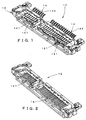
- a connector (plug) 10 of the present embodiment includes a housing 12 and a plurality of contacts 14 as a contact member held by the housing 12.
- the housing 12 is formed of electrically insulating plastic and may be fabricated by a known injection molding technique.
- the material is appropriately selected in consideration of dimensional stability, workability, cost, and the like, and generally selected from polybutylene terephthalate (PBT), polyamide (66PA, 46PA), a liquid crystal polymer (LCP), polycarbonate (PC), polytetrafluoroethylene (PTFE) or a synthetic material thereof.
- the housing 12 is provided with a desired number of insertion holes 121 through which the contact 14 are to be inserted and a fitting opening in which FPC or FFC is inserted.
- the contacts 14 are held in the housing 12 by welding, but the contacts 14 may be held in the housing 12 by a known technique such as press fitting or engaging.
- each of the contacts 14 includes a contact portion 141 that is adapted to come into contact with a connector (receptacle), which is an object to be connected, not shown, and a connecting portion 143 adapted to be connected to a substrate or a cable, and the contacts 14 can be fabricated by a known processing method such as pressing or machining.
- the contact 14, particularly at least the contact portion 141 of the contact 14 includes an undercoat plating layer 147 stacked on a surface portion of a conductive substrate 145 and a main plating layer 149 on the undercoat plating layer 147.
- conductive substrate 145 is made of known various kinds of metal, e.g., made of copper or made of a copper alloy.
- the copper alloy may be phosphor bronze, beryllium copper, brass, or the like, and it is preferable that it is made of phosphor bronze when corrosion resistance is of importance.
- the main plating layer 149 is one of Au-containing plating, Ag-containing plating, Pd-containing plating, Pd-Ni plating, Sn plating and Sn-based alloy plating. This is because contact stability, corrosion resistance and solder wettability are good. Also, it is preferable that the main plating layer 149 is an Au-containing plating when corrosion resistance is of particular importance.
- the main plating layer 149 has a thickness of 0.03 ⁇ m to 6.0 ⁇ m, although it depends on the material of the main plating.
- the thickness is about 0.1 ⁇ m to 1.0 ⁇ m for a portion where electric reliability is necessary (contact portion) and about 0.03 ⁇ m to 0.20 ⁇ m for a portion where reliability of the soldering is necessary.
- the main plating layer 149 is a Pd-containing plating or a Pd-Ni plating
- the main plating layer 149 comprising an Au-containing plating layer or a Pd-containing plating layer may have a thickness of greater than 1.0 ⁇ m, but considering the cost, it is preferable that a thickness is less than or equal to 1.0 ⁇ m, and it is more preferable that a thickness is less than or equal to 0.4 ⁇ m.
- the thickness is preferably 2.0 ⁇ m to 6.0 ⁇ m to ensure good electrical reliability and soldering reliability.
- the undercoat plating layer 147 is one of a Ni-P plating layer, a Ni plating layer, a Pd-Ni plating layer, and a composite plating layer of a Ni plating layer and a Pd-Ni plating layer.
- the undercoat plating layer 147 is a Ni-P plating layer.
- P density is 2.0 weight % to 18 weight %. This is because when P concentration is less than 2.0 weight %, corrosion resistance might decrease, and when P concentration is greater than 18 weight %, ductility is poor and could cause breaks such as cracks.
- the Ni-P plating layer has a thickness of 0.5 ⁇ m to 6.0 ⁇ m. This is because, in a case where the thickness is less than 0.5 ⁇ m, corrosion resistance might decrease due to diffusion of copper, zinc, etc., that are included in the copper alloy, and when it is greater than 6.0 ⁇ m, ductility is poor and could cause breaks such as cracks.
- the Ni-P plating layer can be formed, for example, by an electroplating method using a Watts bath or a sulfamate bath. Particularly, it is preferable to be formed by an electroplating method using a bath based on sulfuric acid in which phosphorous acid is added to a Watt bath. This is because it is possible to form a layer in which crystals are dense, a surface activity is high, and an interface reactivity with the main plating layer 149 such as Au of the upper layer is good.
- the connector 10 includes a coating 16 containing a fluorine system oil on at least the surface of the contact portion 141 on the main plating layer 149 of the contact 14.
- the coating 16 for improving corrosion resistance needs not only protect the contact 14 from oxygen, moisture, and corrosive gas, but also not to inhibit electricity property. Further, it is required to have heat resistance such that detaching or resolving does not occur at a mounting temperature (up to 260 °C), have lubricity, have a small surface tension and an improved uniform dispersibility (self-recovery capacity), and further inert to chloride ions and sulfate ions.
- the fluorine-based oil may include perfluoropolyether-based oils (PFPE oils), and among these, it is particularly preferable to use a perfluoropolyether-based oil (PFPE) which is a polymeric fluorine-based compound having a skeleton of [-CF 2 -O-], a surface tension (25 °C) of less than or equal to 25 mN/m, and a mean molecular weight of 500 to 15,000.
- PFPE perfluoropolyether-based oils
- Perfluoropolyether-based oils may be those having structural formulae indicated in Table 1 below.
- SANKOL ZZS-202 (SANKOL ZZS-202) (product name) available from Sankei Kagaku Co., Ltd. (SANKEIKAGAKU CO., LTD.) can be appropriately used.
- a method of forming the coating on the main plating layer 149 includes, for example, immersing the contact 14 in a solution (coating liquid) obtained by diluting a fluorine system oil with a solvent for a few to several seconds (one or more seconds) and evaporating the solvent to form the coating 16 on the surface of the contact 14.
- a solution obtained by diluting a fluorine system oil with a solvent for a few to several seconds (one or more seconds) and evaporating the solvent to form the coating 16 on the surface of the contact 14.
- HFE described below evaporates instantly in about a few to several seconds and thus only PFPE can be remained on the surface of the contact 14.
- Such an application work can be performed continuously by a reel to reel method.
- hydrofluoroether As for the solvent, a fluorine-based solvent which has a good dispersibility with the fluorine-based oil is preferable, and, for example, it is preferable to use hydrofluoroether (HFE). Hydrofluoroether may be those having structural formulae indicated in Table 2 below.
- SANKOLCFD diluent Z (SANKOL CFD DILUENT Z) (product name) which is available from Sankei Kagaku Co., Ltd. (SANKEIKAGAKU CO., LTD.) can be appropriately used.
- the coating 16 of a desired dry coating weight can be readily formed on the surface of contact 14 simply by adjusting the concentration of the coating liquid.
- the relationship between the concentration of the PFPE oil to HFE and the dry coating weight of the coating was examined using a test piece including a Ni plating layer and an Au plating layer formed on a pure copper plate, and the results are indicated in Table 3 below.
- corrosion resistance can be improved by forming the coating 16 containing fluorine-based oil on the surface of the contact 14, but in order to obtain corrosion resistance to such an extent to conform with a corrosion resistance test under a severe condition by the four-gas mixture flow while attempting to reduce the thickness of the main plating layer 149, it is essential that the dry coating weight per unit area of the coating 16 is greater than or equal to 0.011 mg/cm 2 . If the dry coating weight per unit area of the coating 16 is less than 0.011 mg/cm 2 , it is difficult to obtain desired corrosion resistance in the corrosion resistance test under such a severe condition stated above, unless the main plating layer 149 is formed with a considerable thickness. This is because an effect of protecting the undercoat plating layer 147 by cooperation of the main plating layer 149 and the coating 16 cannot be obtained sufficiently.
- the dry coating weight of the coating 16 is greater than or equal to 0.25 mg/cm 2 , it is preferable since a good corrosion resistance can be obtained in a broader thickness region of the main plating layer 149.
- the dry coating weight per unit area of fluorine-based-oil-containing coating 16 on the main plating layer 149 is greater than or equal to 0.011 mg/cm 2 ; in a case where the main plating layer 149 has a thickness of greater than or equal to 0.2 ⁇ m and less than 0.4 ⁇ m, the dry coating weight of the coating 16 is greater than or equal to 0.04 mg/cm 2 ; in a case where the main plating layer 149 has a thickness of greater than or equal to 0.1 ⁇ m and less than 0.2 ⁇ m; the dry
- the coating 16 deposited by an appropriate amount can protect the contact 10 from oxygen, corrosive gas, moisture, etc., by cooperating with the main plating layer 149, high corrosion resistance can be obtained.
- the fluorine-based oil composing a coating 16 is, because of its fluidity, pushed away into micro recesses in the surface when the contacts come into contact with each other, and thus does not affect conductivity and thus a stable conductivity can be obtained.
- the main plating layer 149 having a thickness of less than or equal to 0.4 ⁇ m, an amount used of an expensive material (gold plating) can be reduced and a large cost cut is possible.
- a conductive substrate formed of phosphor bronze (Cu: remaining mass %, Sn: 6 weight % to 9 weight %, P: 0.3 weight % to 0.35 weight % and incidental impurities) machined into a predetermined contact shape was prepared, and, the conductive substrate was subjected to alkali cathode electrolytic degreasing under the condition of: sodium orthosilicate concentration of 50 g/l; bath temperature of 55 °C; cathode current density of 10 A/dm 2 ; and duration of electrolysis of 30 seconds, rinsed with water, and thereafter subjected to acid cleaning under the condition of: hydrochloric acid concentration of 10 vol %; bath temperature of 20 °C, and immersion duration of 10 seconds.
- alkali cathode electrolytic degreasing under the condition of: sodium orthosilicate concentration of 50 g/l; bath temperature of 55 °C; cathode current density of 10 A/dm 2 ; and duration of electrolysis of 30 seconds, rinsed with water
- a Ni plating layer was formed on a surface portion of phosphor bronze under the condition of: bath composition of a sulphate bath (Watts bath); pH of 4.0; bath temperature of 50 °C; and current density of 10 A/dm 2 , and, further, on this Ni plating layer, an Au plating layer was formed under the condition of: bath composition of gold (I) potassium cyanide (KAu (CN) 2 ) 12.5 g/l; cobalt sulfate (CoSO 4 7H 2 O) of 400 ppm; additive of 12.5 ml/1; bath temperature of 50 °C; and current density of 3A/dm 2 .
- a coating liquid in which PFPE oil is diluted with HFE to a predetermined concentration was applied to form a coating containing PFPE.
- the contact was assembled to the housing shown in FIG. 1 to provide a connector of Sample 1.
- the thickness of the Ni plating layer, the thickness of the Au plating layer, and the dry coating weight of the PFPE-containing coating are as indicated in Table 3.
- "Sankol ZZS-202" (SANKOL ZZS-202) (product name) available from Sankei Kagaku Co., Ltd. (SANKEIKAGAKU CO., LTD.) was used as the PFPE.
- SANKOLCFD diluent Z (SANKOL CFD DILUENT Z) (product name) which is available from Sankei Kagaku Co., Ltd. (SANKEIKAGAKU CO., LTD.) was used as the solvent.
- connectors of samples 2 to 33 that are different from sample 1 merely in their thickness of the Ni plating layer, thickness of the Au plating layer and dry coating weight of the PFPE-containing coating were fabricated.
- the thickness of the Ni plating layer, the thickness of the Au plating layer and the dry coating weight of the PFPE-containing coating are as indicated in Table 4.
- a connector of sample 34 was fabricated with a method similar to a method for sample 1 except that the Ni plating layer was replaced with an electrolysis Ni-P plating layer formed under the condition of: bath composition of sulphate bath (phosphorous acid component); pH of 2.5; bath temperature of 60 °C; and current density of 10A/dm 2 .
- the thickness of the Ni plating layer, thickness of the Au plating layer and the dry coating weight of the PFPE-containing coating are as shown in Table 4.
- Connectors of samples 35 to 37 were fabricated with a method similar to a method for sample 1 except that a Pd-Ni plating layer was formed between the Ni plating layer and the Au plating layer under a condition of: bath composition of a low ammonia bath; PH of 7.5; bath temperature of 45 °C; and current density of 10A/dm 2 .
- the thickness of the Pd-Ni/Ni plating, thickness of the Au plating and the dry coating weight of the PFPE-containing coating are as shown in Table 4.
- a connector of sample 38 was fabricated with a method similar to a method for sample 1 except that the Au plating layer was replaced with a Ag plating layer under a condition that: bath composition of a cyanidation bath; PH of 12; bath temperature of 15 °C to 25 °C; and current density of 2A/dm 2 .
- the thickness of the Ni plating layer, the thickness of the Ag plating layer and the dry coating weight of the PFPE-containing coating are as shown in Table 4.
- Connectors of samples 39 to 72 were fabricated with a method similar to a method for sample 1 except that the thickness of the Au plating layer and the dry coating weight of PFPE-containing coating were out of scope of the present invention.
- a connector of sample 73 was fabricated with a method similar to a method for sample 1 except that the PFPE-containing coating was replaced with a benzothiazole-based water-soluble corrosion preventing agent applied on the Au plating layer.
- a connector of sample 74 was fabricated with a method similar to a method for sample 73 except that an electrolysis Ni-P plating layer was formed in place of the Ni plating layer.
- a connector of sample 75 was fabricated with a method similar to a method for sample 73 except that a thiol solvent-based corrosion preventing agent of was applied on the Au plating layer in place of the benzothiazole-based water-soluble corrosion preventing agent.
- a corrosion resistance test was conducted by steps (a) to (e) below.
- the four-gas mixture test complies with EIA standard (EIA-364-65A), and type and density of gases are: H 2 S 10 ⁇ 5 ppb; SO 2 100 ⁇ 20 ppb; NO 2 200 ⁇ 50 ppb; Cl 2 10 ⁇ 3 ppb; temperature 30 °C; and humidity 75% RH.
- EIA-364-65A EIA-364-65A
- Table 5 shows the above evaluation results that are summarized based on the relationship between the thickness of the main plating layer and the dry coating weight of the PFPE-containing coating.
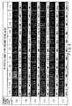
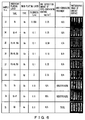
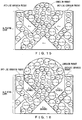
- FIG. 5 photographic images of surfaces of the contacts of the connectors of samples 1 to 32 and samples 39 to 72 after the test are shown in FIG. 5 . Further, photographic images the contacts of the connectors of samples 33 to 38 and samples 73 to 75 after the test are shown in FIG. 6 .
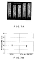
- FIG. 7A shows an example of the surface condition observation result of the contacts after the salt spray test, and generation of a corrosion product due to the salt spray test was not clearly observed.
- FIG. 7B shows contact resistance values before and after the test, and it can be seen that there was almost no increase in contact resistance due to the salt spray test and it was within the standard (twice the initial contact resistance value or less). Therefore, it became clear that the connector to which the present invention was applied had a high corrosion resistance to the salt spray test.
- the two-gas mixture test satisfies conditions standardized among electronic equipment set manufacturers, and type and density of gases are: H 2 S 3 ppm; SO 2 10 ppm; temperature of 40 °C; and humidity of 75% RH.
- FIG. 8A shows an exemplary surface condition observation result of contacts after the two-gas mixture test, and although the two-gas mixture test is partially an atmosphere that was more severe than a three-gas mixture test and a four-gas mixture test (gas concentration of an order of a few to several ppm, and 500 times of insertion and extraction), a corrosion product was not clearly produced. Also, FIG.
- a nitric acid vapor test complying with an EIA standard (EIA-364-53B) is carried out unmated with a counterpart connector and under a condition of: temperature 23 °C; nitric acid 300 ml (specific gravity 1.42); desiccator volume 6L; and test duration of 75 minutes. Note that, for a nitric acid vapor test, there is no standard for measurement of a contact resistance value and thus only surface observation was performed.
- a method of counting corrosion products is as shown in Table 6 below. For example, in a case where the size of the corrosion product is 0.05 mm or smaller, the corrosion product is counted as zero.
- PFPE oil is composed primarily of C (carbon) and F (fluorine), these elements are surely detected by using an electron beam micro analyzer. Other than this, although the resolution is lower, detection is possible by EDX (energy dispersed type).
- the PFPE oil is composed primarily of C (carbon), F (fluorine) and O (oxygen), and it is a polymeric compound having a "-CF2-O-" skeleton, infrared absorption peaks originating from bonds between them appear. That is, an absorption peak of a high intensity will appear at 1300 to 1000 cm -1 for a fluorine-based compound. Also, the PFPE oil includes an ether linkage (C-O-C), and thus an absorption peak originating from this also appears (it does not appear for polytetrafluoroethylene or the like). In addition, in a case where a CH group is included, an absorption peak appears around 3000 to 2800 cm -1 about.
- the PFPE oil has a low concentration
- the detected elements are C (carbon), F (fluorine) and O (oxygen).
- the bonding energy (horizontal axis) with respect to a photoelectric peak of each elemental (vertical axis) shifts depending on the bonding state (chemical shift).
- an electronic component showing an excellent corrosion resistance to the four-gas mixture flow with an inexpensive structure can be provided.
Landscapes
- Chemical & Material Sciences (AREA)
- Engineering & Computer Science (AREA)
- Chemical Kinetics & Catalysis (AREA)
- Electrochemistry (AREA)
- Materials Engineering (AREA)
- Metallurgy (AREA)
- Organic Chemistry (AREA)
- Crystallography & Structural Chemistry (AREA)
- Electroplating Methods And Accessories (AREA)
- Preventing Corrosion Or Incrustation Of Metals (AREA)
Applications Claiming Priority (3)
| Application Number | Priority Date | Filing Date | Title |
|---|---|---|---|
| JP2013095416 | 2013-04-30 | ||
| JP2013156056 | 2013-07-26 | ||
| PCT/JP2014/059942 WO2014178259A1 (ja) | 2013-04-30 | 2014-04-04 | 電子部品 |
Publications (3)
| Publication Number | Publication Date |
|---|---|
| EP2993253A1 true EP2993253A1 (de) | 2016-03-09 |
| EP2993253A4 EP2993253A4 (de) | 2017-01-04 |
| EP2993253B1 EP2993253B1 (de) | 2020-03-11 |
Family
ID=51843394
Family Applications (1)
| Application Number | Title | Priority Date | Filing Date |
|---|---|---|---|
| EP14791907.0A Active EP2993253B1 (de) | 2013-04-30 | 2014-04-04 | Elektronische komponente |
Country Status (7)
| Country | Link |
|---|---|
| US (1) | US9705221B2 (de) |
| EP (1) | EP2993253B1 (de) |
| JP (1) | JP6224090B2 (de) |
| KR (1) | KR101788688B1 (de) |
| CN (1) | CN105189823B (de) |
| ES (1) | ES2787575T3 (de) |
| WO (1) | WO2014178259A1 (de) |
Families Citing this family (9)
| Publication number | Priority date | Publication date | Assignee | Title |
|---|---|---|---|---|
| CN105358741B (zh) * | 2013-06-10 | 2018-04-20 | 东方镀金株式会社 | 镀敷叠层体的制造方法及镀敷叠层体 |
| JP7011142B2 (ja) | 2016-09-30 | 2022-01-26 | 日亜化学工業株式会社 | 発光装置、発光装置用パッケージ及び発光装置の製造方法 |
| US9859640B1 (en) * | 2016-11-14 | 2018-01-02 | Te Connectivity Corporation | Electrical connector with plated signal contacts |
| US11152729B2 (en) * | 2016-11-14 | 2021-10-19 | TE Connectivity Services Gmbh | Electrical connector and electrical connector assembly having a mating array of signal and ground contacts |
| USD979507S1 (en) * | 2018-12-21 | 2023-02-28 | Molex, Llc | Connector |
| JP7505679B2 (ja) * | 2019-03-27 | 2024-06-25 | サムソン エレクトロ-メカニックス カンパニーリミテッド. | 積層型キャパシタ |
| MY205981A (en) * | 2019-06-05 | 2024-11-22 | Erni Int Ag | Electrical contact element |
| DE102019115243A1 (de) * | 2019-06-05 | 2020-12-10 | Erni International Ag | Elektrisches Kontaktelement für hohe Betriebsspannungen |
| DE102024107929A1 (de) * | 2024-03-20 | 2025-09-25 | Weidmüller Interface GmbH & Co. KG | Steckverbindung, insbesondere Daten- und Leistungssteckverbindung und Verfahren zur Herstellung eines Steckverbinders |
Family Cites Families (16)
| Publication number | Priority date | Publication date | Assignee | Title |
|---|---|---|---|---|
| US4268568A (en) * | 1979-05-14 | 1981-05-19 | Bell Telephone Laboratories, Incorporated | Lubricated electrical contacts |
| JPS5790891A (en) * | 1980-11-26 | 1982-06-05 | Ngk Spark Plug Co | Ignition plug |
| JPS59189196A (ja) * | 1983-04-13 | 1984-10-26 | Showa Denko Kk | 銀メツキコネクタ−の潤滑防錆剤 |
| JPS60251285A (ja) | 1984-05-25 | 1985-12-11 | Showa Denko Kk | 電気接点のめつき用表面処理剤 |
| JPH0822858A (ja) | 1994-07-06 | 1996-01-23 | Fuji Electric Co Ltd | 開閉機器摺動部品の摺動抵抗低減方法 |
| JP2002343168A (ja) | 2001-05-11 | 2002-11-29 | Mitsubishi Electric Corp | 摺動通電体 |
| JP2004307954A (ja) * | 2003-04-08 | 2004-11-04 | Matsushita Electric Works Ltd | めっき形成部材 |
| JP4083084B2 (ja) | 2003-06-24 | 2008-04-30 | 株式会社神戸製鋼所 | コネクタ接点材料および多極端子 |
| JP4348288B2 (ja) | 2004-12-20 | 2009-10-21 | 株式会社神戸製鋼所 | コネクタ接点材料 |
| KR100702956B1 (ko) | 2005-04-26 | 2007-04-03 | 삼성테크윈 주식회사 | 반도체 팩키지용 리드프레임 및 그 제조 방법 |
| JP2009099282A (ja) * | 2007-10-12 | 2009-05-07 | Kobe Steel Ltd | 嵌合型コネクタ |
| JPWO2010005088A1 (ja) | 2008-07-11 | 2012-01-05 | 第一電子工業株式会社 | 電子部品およびその製造方法 |
| JP2010180425A (ja) * | 2009-02-03 | 2010-08-19 | Alps Electric Co Ltd | 電気接点及びその製造方法 |
| JP2012007228A (ja) * | 2010-06-28 | 2012-01-12 | Jst Mfg Co Ltd | 電子部品 |
| EP2533368A1 (de) * | 2011-06-10 | 2012-12-12 | Delphi Technologies, Inc. | Verfahren zur Herstellung einer Gleitkontaktanordnung |
| EP2904665A4 (de) * | 2012-10-04 | 2016-05-04 | Fci Asia Pte Ltd | Elektrischer kontakt mit korrosionsbeständiger beschichtung |
-
2014
- 2014-04-04 KR KR1020157034155A patent/KR101788688B1/ko active Active
- 2014-04-04 ES ES14791907T patent/ES2787575T3/es active Active
- 2014-04-04 US US14/784,778 patent/US9705221B2/en active Active
- 2014-04-04 WO PCT/JP2014/059942 patent/WO2014178259A1/ja not_active Ceased
- 2014-04-04 CN CN201480024619.4A patent/CN105189823B/zh active Active
- 2014-04-04 EP EP14791907.0A patent/EP2993253B1/de active Active
- 2014-04-04 JP JP2015514793A patent/JP6224090B2/ja active Active
Also Published As
| Publication number | Publication date |
|---|---|
| JPWO2014178259A1 (ja) | 2017-02-23 |
| CN105189823B (zh) | 2018-01-02 |
| KR20160003222A (ko) | 2016-01-08 |
| WO2014178259A1 (ja) | 2014-11-06 |
| CN105189823A (zh) | 2015-12-23 |
| EP2993253A4 (de) | 2017-01-04 |
| US9705221B2 (en) | 2017-07-11 |
| EP2993253B1 (de) | 2020-03-11 |
| US20160064846A1 (en) | 2016-03-03 |
| JP6224090B2 (ja) | 2017-11-01 |
| ES2787575T3 (es) | 2020-10-16 |
| KR101788688B1 (ko) | 2017-10-20 |
Similar Documents
| Publication | Publication Date | Title |
|---|---|---|
| EP2993253B1 (de) | Elektronische komponente | |
| EP2829637B1 (de) | Metallisches material für elektronisches bauteil, damit hergestellte anschlussklemme, verbinder und elektronisches bauteil | |
| KR102058344B1 (ko) | 전자 부품용 금속 재료 및 그 제조 방법, 그것을 사용한 커넥터 단자, 커넥터 및 전자 부품 | |
| RU2566103C1 (ru) | Металлический материал для электронного компонента и способ его изготовления | |
| EP2868776B1 (de) | Metallmaterial für elektronische bauteile und herstellungsverfahren dafür sowie verbindungsendstück, steckverbinder und elektronisches bauteil mit diesem metallmaterial für elektronische bauteile | |
| JP5968668B2 (ja) | 電子部品用金属材料 | |
| EP2173012B1 (de) | Reibverschleissbeständiger verbinder und verfahren zu seiner herstellung | |
| EP2868772B1 (de) | Metallmaterial für ein elektronisches bauteil, herstellungsverfahren dafür sowie verbindungsendstück, verbinder und elektronisches bauteil mit dem metallmaterial für ein elektronisches bauteil | |
| CN101821431B (zh) | 连接器制造方法和通过该方法制造的连接器 | |
| EP2154688A1 (de) | Elektrisches kontaktmaterial, verfahren zur herstellung des elektrischen kontaktmaterials und elektrischer kontakt | |
| TWI443232B (zh) | A metal material, a method for manufacturing the same, and an electrical and electronic part using the same | |
| CN104471113A (zh) | 电子部件用金属材料及其制造方法、使用其的连接器端子、连接器及电子部件 | |
| TWI449809B (zh) | Electrical and electronic components for the use of composite materials and electrical and electronic components | |
| CN110199054B (zh) | 表面处理镀敷材料、连接器端子、连接器、ffc端子、ffc、fpc及电子零件 | |
| JP5464284B1 (ja) | コネクタ端子及びコネクタ端子の製造方法 | |
| JP6503159B2 (ja) | 電子部品用金属材料、それを用いたコネクタ端子、コネクタ及び電子部品 | |
| EP4131306B1 (de) | Kontaktelement, verbinder, zusammensetzung und verfahren zur herstellung eines kontaktelements | |
| EP4365329A1 (de) | Verbundstoff, verbundstoffherstellungsverfahren, endgerät und endgeräteherstellungsverfahren | |
| CN120265834A (zh) | 复合材料、端子以及端子的制造方法 |
Legal Events
| Date | Code | Title | Description |
|---|---|---|---|
| PUAI | Public reference made under article 153(3) epc to a published international application that has entered the european phase |
Free format text: ORIGINAL CODE: 0009012 |
|
| 17P | Request for examination filed |
Effective date: 20151124 |
|
| AK | Designated contracting states |
Kind code of ref document: A1 Designated state(s): AL AT BE BG CH CY CZ DE DK EE ES FI FR GB GR HR HU IE IS IT LI LT LU LV MC MK MT NL NO PL PT RO RS SE SI SK SM TR |
|
| AX | Request for extension of the european patent |
Extension state: BA ME |
|
| DAX | Request for extension of the european patent (deleted) | ||
| A4 | Supplementary search report drawn up and despatched |
Effective date: 20161206 |
|
| RIC1 | Information provided on ipc code assigned before grant |
Ipc: C23F 11/00 20060101ALI20161129BHEP Ipc: H01R 13/11 20060101ALI20161129BHEP Ipc: C23F 17/00 20060101AFI20161129BHEP Ipc: C25D 7/00 20060101ALI20161129BHEP Ipc: H01R 13/03 20060101ALI20161129BHEP Ipc: C25D 5/12 20060101ALI20161129BHEP Ipc: C25D 5/48 20060101ALI20161129BHEP |
|
| STAA | Information on the status of an ep patent application or granted ep patent |
Free format text: STATUS: EXAMINATION IS IN PROGRESS |
|
| 17Q | First examination report despatched |
Effective date: 20180716 |
|
| GRAP | Despatch of communication of intention to grant a patent |
Free format text: ORIGINAL CODE: EPIDOSNIGR1 |
|
| STAA | Information on the status of an ep patent application or granted ep patent |
Free format text: STATUS: GRANT OF PATENT IS INTENDED |
|
| RIC1 | Information provided on ipc code assigned before grant |
Ipc: C23F 11/00 20060101ALI20190920BHEP Ipc: C25D 5/34 20060101ALN20190920BHEP Ipc: C25D 5/12 20060101ALI20190920BHEP Ipc: C25D 3/12 20060101ALN20190920BHEP Ipc: H01R 13/11 20060101ALI20190920BHEP Ipc: H01R 24/62 20110101ALN20190920BHEP Ipc: C25D 7/00 20060101ALI20190920BHEP Ipc: C25D 5/48 20060101ALI20190920BHEP Ipc: H01R 13/03 20060101ALI20190920BHEP Ipc: C25D 3/48 20060101ALN20190920BHEP Ipc: C23F 17/00 20060101AFI20190920BHEP |
|
| INTG | Intention to grant announced |
Effective date: 20191017 |
|
| GRAS | Grant fee paid |
Free format text: ORIGINAL CODE: EPIDOSNIGR3 |
|
| GRAA | (expected) grant |
Free format text: ORIGINAL CODE: 0009210 |
|
| STAA | Information on the status of an ep patent application or granted ep patent |
Free format text: STATUS: THE PATENT HAS BEEN GRANTED |
|
| AK | Designated contracting states |
Kind code of ref document: B1 Designated state(s): AL AT BE BG CH CY CZ DE DK EE ES FI FR GB GR HR HU IE IS IT LI LT LU LV MC MK MT NL NO PL PT RO RS SE SI SK SM TR |
|
| REG | Reference to a national code |
Ref country code: GB Ref legal event code: FG4D |
|
| REG | Reference to a national code |
Ref country code: CH Ref legal event code: EP |
|
| REG | Reference to a national code |
Ref country code: AT Ref legal event code: REF Ref document number: 1243241 Country of ref document: AT Kind code of ref document: T Effective date: 20200315 |
|
| REG | Reference to a national code |
Ref country code: IE Ref legal event code: FG4D |
|
| REG | Reference to a national code |
Ref country code: DE Ref legal event code: R096 Ref document number: 602014062228 Country of ref document: DE |
|
| PG25 | Lapsed in a contracting state [announced via postgrant information from national office to epo] |
Ref country code: FI Free format text: LAPSE BECAUSE OF FAILURE TO SUBMIT A TRANSLATION OF THE DESCRIPTION OR TO PAY THE FEE WITHIN THE PRESCRIBED TIME-LIMIT Effective date: 20200311 Ref country code: NO Free format text: LAPSE BECAUSE OF FAILURE TO SUBMIT A TRANSLATION OF THE DESCRIPTION OR TO PAY THE FEE WITHIN THE PRESCRIBED TIME-LIMIT Effective date: 20200611 Ref country code: RS Free format text: LAPSE BECAUSE OF FAILURE TO SUBMIT A TRANSLATION OF THE DESCRIPTION OR TO PAY THE FEE WITHIN THE PRESCRIBED TIME-LIMIT Effective date: 20200311 |
|
| REG | Reference to a national code |
Ref country code: NL Ref legal event code: MP Effective date: 20200311 |
|
| PG25 | Lapsed in a contracting state [announced via postgrant information from national office to epo] |
Ref country code: GR Free format text: LAPSE BECAUSE OF FAILURE TO SUBMIT A TRANSLATION OF THE DESCRIPTION OR TO PAY THE FEE WITHIN THE PRESCRIBED TIME-LIMIT Effective date: 20200612 Ref country code: BG Free format text: LAPSE BECAUSE OF FAILURE TO SUBMIT A TRANSLATION OF THE DESCRIPTION OR TO PAY THE FEE WITHIN THE PRESCRIBED TIME-LIMIT Effective date: 20200611 Ref country code: HR Free format text: LAPSE BECAUSE OF FAILURE TO SUBMIT A TRANSLATION OF THE DESCRIPTION OR TO PAY THE FEE WITHIN THE PRESCRIBED TIME-LIMIT Effective date: 20200311 Ref country code: LV Free format text: LAPSE BECAUSE OF FAILURE TO SUBMIT A TRANSLATION OF THE DESCRIPTION OR TO PAY THE FEE WITHIN THE PRESCRIBED TIME-LIMIT Effective date: 20200311 Ref country code: SE Free format text: LAPSE BECAUSE OF FAILURE TO SUBMIT A TRANSLATION OF THE DESCRIPTION OR TO PAY THE FEE WITHIN THE PRESCRIBED TIME-LIMIT Effective date: 20200311 |
|
| REG | Reference to a national code |
Ref country code: LT Ref legal event code: MG4D |
|
| PG25 | Lapsed in a contracting state [announced via postgrant information from national office to epo] |
Ref country code: NL Free format text: LAPSE BECAUSE OF FAILURE TO SUBMIT A TRANSLATION OF THE DESCRIPTION OR TO PAY THE FEE WITHIN THE PRESCRIBED TIME-LIMIT Effective date: 20200311 |
|
| REG | Reference to a national code |
Ref country code: ES Ref legal event code: FG2A Ref document number: 2787575 Country of ref document: ES Kind code of ref document: T3 Effective date: 20201016 |
|
| PG25 | Lapsed in a contracting state [announced via postgrant information from national office to epo] |
Ref country code: PT Free format text: LAPSE BECAUSE OF FAILURE TO SUBMIT A TRANSLATION OF THE DESCRIPTION OR TO PAY THE FEE WITHIN THE PRESCRIBED TIME-LIMIT Effective date: 20200805 Ref country code: IS Free format text: LAPSE BECAUSE OF FAILURE TO SUBMIT A TRANSLATION OF THE DESCRIPTION OR TO PAY THE FEE WITHIN THE PRESCRIBED TIME-LIMIT Effective date: 20200711 Ref country code: CZ Free format text: LAPSE BECAUSE OF FAILURE TO SUBMIT A TRANSLATION OF THE DESCRIPTION OR TO PAY THE FEE WITHIN THE PRESCRIBED TIME-LIMIT Effective date: 20200311 Ref country code: SK Free format text: LAPSE BECAUSE OF FAILURE TO SUBMIT A TRANSLATION OF THE DESCRIPTION OR TO PAY THE FEE WITHIN THE PRESCRIBED TIME-LIMIT Effective date: 20200311 Ref country code: LT Free format text: LAPSE BECAUSE OF FAILURE TO SUBMIT A TRANSLATION OF THE DESCRIPTION OR TO PAY THE FEE WITHIN THE PRESCRIBED TIME-LIMIT Effective date: 20200311 Ref country code: RO Free format text: LAPSE BECAUSE OF FAILURE TO SUBMIT A TRANSLATION OF THE DESCRIPTION OR TO PAY THE FEE WITHIN THE PRESCRIBED TIME-LIMIT Effective date: 20200311 Ref country code: EE Free format text: LAPSE BECAUSE OF FAILURE TO SUBMIT A TRANSLATION OF THE DESCRIPTION OR TO PAY THE FEE WITHIN THE PRESCRIBED TIME-LIMIT Effective date: 20200311 Ref country code: SM Free format text: LAPSE BECAUSE OF FAILURE TO SUBMIT A TRANSLATION OF THE DESCRIPTION OR TO PAY THE FEE WITHIN THE PRESCRIBED TIME-LIMIT Effective date: 20200311 |
|
| REG | Reference to a national code |
Ref country code: AT Ref legal event code: MK05 Ref document number: 1243241 Country of ref document: AT Kind code of ref document: T Effective date: 20200311 |
|
| REG | Reference to a national code |
Ref country code: CH Ref legal event code: PL |
|
| REG | Reference to a national code |
Ref country code: DE Ref legal event code: R097 Ref document number: 602014062228 Country of ref document: DE |
|
| PG25 | Lapsed in a contracting state [announced via postgrant information from national office to epo] |
Ref country code: MC Free format text: LAPSE BECAUSE OF FAILURE TO SUBMIT A TRANSLATION OF THE DESCRIPTION OR TO PAY THE FEE WITHIN THE PRESCRIBED TIME-LIMIT Effective date: 20200311 |
|
| PLBE | No opposition filed within time limit |
Free format text: ORIGINAL CODE: 0009261 |
|
| STAA | Information on the status of an ep patent application or granted ep patent |
Free format text: STATUS: NO OPPOSITION FILED WITHIN TIME LIMIT |
|
| PG25 | Lapsed in a contracting state [announced via postgrant information from national office to epo] |
Ref country code: CH Free format text: LAPSE BECAUSE OF NON-PAYMENT OF DUE FEES Effective date: 20200430 Ref country code: LI Free format text: LAPSE BECAUSE OF NON-PAYMENT OF DUE FEES Effective date: 20200430 Ref country code: LU Free format text: LAPSE BECAUSE OF NON-PAYMENT OF DUE FEES Effective date: 20200404 Ref country code: IT Free format text: LAPSE BECAUSE OF FAILURE TO SUBMIT A TRANSLATION OF THE DESCRIPTION OR TO PAY THE FEE WITHIN THE PRESCRIBED TIME-LIMIT Effective date: 20200311 Ref country code: DK Free format text: LAPSE BECAUSE OF FAILURE TO SUBMIT A TRANSLATION OF THE DESCRIPTION OR TO PAY THE FEE WITHIN THE PRESCRIBED TIME-LIMIT Effective date: 20200311 Ref country code: AT Free format text: LAPSE BECAUSE OF FAILURE TO SUBMIT A TRANSLATION OF THE DESCRIPTION OR TO PAY THE FEE WITHIN THE PRESCRIBED TIME-LIMIT Effective date: 20200311 |
|
| REG | Reference to a national code |
Ref country code: BE Ref legal event code: MM Effective date: 20200430 |
|
| 26N | No opposition filed |
Effective date: 20201214 |
|
| PG25 | Lapsed in a contracting state [announced via postgrant information from national office to epo] |
Ref country code: PL Free format text: LAPSE BECAUSE OF FAILURE TO SUBMIT A TRANSLATION OF THE DESCRIPTION OR TO PAY THE FEE WITHIN THE PRESCRIBED TIME-LIMIT Effective date: 20200311 Ref country code: BE Free format text: LAPSE BECAUSE OF NON-PAYMENT OF DUE FEES Effective date: 20200430 Ref country code: SI Free format text: LAPSE BECAUSE OF FAILURE TO SUBMIT A TRANSLATION OF THE DESCRIPTION OR TO PAY THE FEE WITHIN THE PRESCRIBED TIME-LIMIT Effective date: 20200311 |
|
| PG25 | Lapsed in a contracting state [announced via postgrant information from national office to epo] |
Ref country code: IE Free format text: LAPSE BECAUSE OF NON-PAYMENT OF DUE FEES Effective date: 20200404 |
|
| PG25 | Lapsed in a contracting state [announced via postgrant information from national office to epo] |
Ref country code: TR Free format text: LAPSE BECAUSE OF FAILURE TO SUBMIT A TRANSLATION OF THE DESCRIPTION OR TO PAY THE FEE WITHIN THE PRESCRIBED TIME-LIMIT Effective date: 20200311 Ref country code: MT Free format text: LAPSE BECAUSE OF FAILURE TO SUBMIT A TRANSLATION OF THE DESCRIPTION OR TO PAY THE FEE WITHIN THE PRESCRIBED TIME-LIMIT Effective date: 20200311 Ref country code: CY Free format text: LAPSE BECAUSE OF FAILURE TO SUBMIT A TRANSLATION OF THE DESCRIPTION OR TO PAY THE FEE WITHIN THE PRESCRIBED TIME-LIMIT Effective date: 20200311 |
|
| PG25 | Lapsed in a contracting state [announced via postgrant information from national office to epo] |
Ref country code: MK Free format text: LAPSE BECAUSE OF FAILURE TO SUBMIT A TRANSLATION OF THE DESCRIPTION OR TO PAY THE FEE WITHIN THE PRESCRIBED TIME-LIMIT Effective date: 20200311 Ref country code: AL Free format text: LAPSE BECAUSE OF FAILURE TO SUBMIT A TRANSLATION OF THE DESCRIPTION OR TO PAY THE FEE WITHIN THE PRESCRIBED TIME-LIMIT Effective date: 20200311 |
|
| P01 | Opt-out of the competence of the unified patent court (upc) registered |
Effective date: 20230531 |
|
| PGFP | Annual fee paid to national office [announced via postgrant information from national office to epo] |
Ref country code: DE Payment date: 20250430 Year of fee payment: 12 |
|
| PGFP | Annual fee paid to national office [announced via postgrant information from national office to epo] |
Ref country code: ES Payment date: 20250513 Year of fee payment: 12 |
|
| REG | Reference to a national code |
Ref country code: DE Ref legal event code: R081 Ref document number: 602014062228 Country of ref document: DE Owner name: FUJIKURA LTD., JP Free format text: FORMER OWNER: DDK LTD., TOKIO/TOKYO, JP |
|
| PGFP | Annual fee paid to national office [announced via postgrant information from national office to epo] |
Ref country code: GB Payment date: 20260313 Year of fee payment: 13 |
|
| PGFP | Annual fee paid to national office [announced via postgrant information from national office to epo] |
Ref country code: FR Payment date: 20260309 Year of fee payment: 13 |
|
| REG | Reference to a national code |
Ref country code: GB Ref legal event code: 732E Free format text: REGISTERED BETWEEN 20260326 AND 20260401 |