EP2995368A1 - Method for manufacturing nanoholes and filter manufactured by the same - Google Patents
Method for manufacturing nanoholes and filter manufactured by the same Download PDFInfo
- Publication number
- EP2995368A1 EP2995368A1 EP15153186.0A EP15153186A EP2995368A1 EP 2995368 A1 EP2995368 A1 EP 2995368A1 EP 15153186 A EP15153186 A EP 15153186A EP 2995368 A1 EP2995368 A1 EP 2995368A1
- Authority
- EP
- European Patent Office
- Prior art keywords
- particles
- hole
- nanoholes
- injected
- outlet
- Prior art date
- Legal status (The legal status is an assumption and is not a legal conclusion. Google has not performed a legal analysis and makes no representation as to the accuracy of the status listed.)
- Granted
Links
Images



Classifications
-
- B—PERFORMING OPERATIONS; TRANSPORTING
- B01—PHYSICAL OR CHEMICAL PROCESSES OR APPARATUS IN GENERAL
- B01D—SEPARATION
- B01D71/00—Semi-permeable membranes for separation processes or apparatus characterised by the material; Manufacturing processes specially adapted therefor
- B01D71/02—Inorganic material
- B01D71/024—Oxides
- B01D71/025—Aluminium oxide
-
- B—PERFORMING OPERATIONS; TRANSPORTING
- B01—PHYSICAL OR CHEMICAL PROCESSES OR APPARATUS IN GENERAL
- B01D—SEPARATION
- B01D69/00—Semi-permeable membranes for separation processes or apparatus characterised by their form, structure or properties; Manufacturing processes specially adapted therefor
-
- B—PERFORMING OPERATIONS; TRANSPORTING
- B01—PHYSICAL OR CHEMICAL PROCESSES OR APPARATUS IN GENERAL
- B01D—SEPARATION
- B01D67/00—Processes specially adapted for manufacturing semi-permeable membranes for separation processes or apparatus
- B01D67/0081—After-treatment of organic or inorganic membranes
- B01D67/0088—Physical treatment with compounds, e.g. swelling, coating or impregnation
-
- C—CHEMISTRY; METALLURGY
- C01—INORGANIC CHEMISTRY
- C01B—NON-METALLIC ELEMENTS; COMPOUNDS THEREOF; METALLOIDS OR COMPOUNDS THEREOF NOT COVERED BY SUBCLASS C01C
- C01B32/00—Carbon; Compounds thereof
-
- C—CHEMISTRY; METALLURGY
- C25—ELECTROLYTIC OR ELECTROPHORETIC PROCESSES; APPARATUS THEREFOR
- C25D—PROCESSES FOR THE ELECTROLYTIC OR ELECTROPHORETIC PRODUCTION OF COATINGS; ELECTROFORMING; APPARATUS THEREFOR
- C25D11/00—Electrolytic coating by surface reaction, i.e. forming conversion layers
- C25D11/02—Anodisation
- C25D11/04—Anodisation of aluminium or alloys based thereon
- C25D11/045—Anodisation of aluminium or alloys based thereon for forming AAO templates
-
- C—CHEMISTRY; METALLURGY
- C25—ELECTROLYTIC OR ELECTROPHORETIC PROCESSES; APPARATUS THEREFOR
- C25D—PROCESSES FOR THE ELECTROLYTIC OR ELECTROPHORETIC PRODUCTION OF COATINGS; ELECTROFORMING; APPARATUS THEREFOR
- C25D11/00—Electrolytic coating by surface reaction, i.e. forming conversion layers
- C25D11/02—Anodisation
- C25D11/04—Anodisation of aluminium or alloys based thereon
- C25D11/18—After-treatment, e.g. pore-sealing
-
- B—PERFORMING OPERATIONS; TRANSPORTING
- B01—PHYSICAL OR CHEMICAL PROCESSES OR APPARATUS IN GENERAL
- B01D—SEPARATION
- B01D2323/00—Details relating to membrane preparation
- B01D2323/28—Pore treatments
- B01D2323/283—Reducing the pores
-
- B—PERFORMING OPERATIONS; TRANSPORTING
- B01—PHYSICAL OR CHEMICAL PROCESSES OR APPARATUS IN GENERAL
- B01D—SEPARATION
- B01D67/00—Processes specially adapted for manufacturing semi-permeable membranes for separation processes or apparatus
- B01D67/0039—Inorganic membrane manufacture
- B01D67/0053—Inorganic membrane manufacture by inducing porosity into non porous precursor membranes
- B01D67/006—Inorganic membrane manufacture by inducing porosity into non porous precursor membranes by elimination of segments of the precursor, e.g. nucleation-track membranes, lithography or laser methods
- B01D67/0065—Inorganic membrane manufacture by inducing porosity into non porous precursor membranes by elimination of segments of the precursor, e.g. nucleation-track membranes, lithography or laser methods by anodic oxidation
Definitions
- the present invention relates to a method for manufacturing nanoholes and a filter manufactured by the same, and more particularly, to a method for manufacturing nanoholes, the method being capable of easily manufacturing nanoholes with a size of several to hundreds of nanometers, and to a filter manufactured by the same.
- a nanohole refers to a pore or passage having a nanoscale width, and is used in various fields, such as for a computing device and a memory device.
- the shape limit of a photosensitive film is at least 1 ⁇ m due to optical diffraction of a photo-mask. Therefore, it is, in fact, difficult to realize several nanometer-sized nanoholes through the above techniques.
- the present invention has been made in an effort to provide a method for manufacturing nanoholes and a filter manufactured by the same, having advantages of easily and simply manufacturing nanoholes with a scale of several nanometers or less.
- An exemplary embodiment of the present invention provides a method for manufacturing nanoholes, the method including: a preparing step of preparing a body having a through-hole which passes through two facing surfaces and has a nano- or micro-scale diameter; and a particle injecting step of injecting particles with a smaller diameter than the through-hole into the through-hole to form nanoholes with a smaller scale than the through-hole.
- a plurality of kinds of particles with different sizes may be injected into the through-hole.
- the same kind of particles with the same size may be injected into the through-hole.
- electrically or chemically treated particles may be injected.
- An inlet, through which the particles are injected in the particle injecting step, and an outlet, which is opposite to the inlet, may be formed in an asymmetric structure so that the particles injected in the particle injecting step do not leave the through-hole.
- the diameter of the inlet may be larger than that of the outlet.
- An inlet, to which the particles are injected in the particle injecting step, and an outlet, which is opposite to the inlet, may be formed in a symmetric structure, and the method may further include an outlet reducing step of reducing the diameter of the outlet of the through-hole, between the preparing step and the particle injecting step.
- a filter including: a filter part having a through-hole which penetrates two facing surfaces and has a nano- or micro-scale diameter; and particles inserted into the through-hole and having a smaller diameter than the through-hole, wherein the filter part has nanoholes with a smaller scale than the through-hole by the particles injected into the through-hole.
- the size of the nanoholes may be controlled by adjusting the size of particles injected into the through-hole.
- the particles may have electrically positive or negative polarity by binding to a functional group.
- a surface of the particles may be positively or negatively charged so that an electrically charged electric double layer is formed on the surface of the particle or a region adjacent to the surface.
- the diameter of an inlet, through which the particles are injected may be larger than that of an outlet, which is opposite to the inlet.
- the filter part may be an anodic aluminum oxide (AAO) membrane.
- AAO anodic aluminum oxide
- a method for manufacturing nanoholes can be provided, the method being capable of easily manufacturing nanoholes with a scale of several nanometers or less.
- the size and arrangement of nanoholes can be controlled by adjusting the size of injected particles.
- surface-functionalized nanoholes can be manufactured by performing a chemical or electric treatment on injected particles.
- a filter capable of easily collecting particles even with a size of several nanometers can be provided.
- nanoholes Even particles with a smaller size than nanoholes can be easily collected by surface-functionalizing particles injected in the nanoholes.
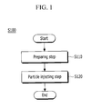
- FIG. 1 is a process flowchart schematically showing a method for manufacturing nanoholes according a first embodiment of the present invention.
- the method S100 for manufacturing nanoholes according to the first embodiment of the present invention, particles with a smaller size than a nano- or micro-scale through-hole 11 are injected into the through-hole 11, and as a result, nanoholes 30 with a size of several nanometers or smaller can be manufactured, wherein the method comprises a preparing step S110 and a particle injecting step S120.
- FIG. 2 is a front view schematically illustrating a preparing step in the method for manufacturing nanoholes shown in FIG. 1 .
- a body 10 which passes through two facing surfaces and has a through-hole 11 with a nano- or micro-scale diameter is prepared.
- the through-hole 11 may be formed to pass through upper and lower surfaces of the body 10, or right and left surfaces of the body 10.
- the through-hole 11 is prepared such that, based on a direction in which particles 20 are injected in the below-described particle injecting step S120, an inlet 11 a, through which the particles 20 are injected, and an outlet 11 b, which is opposite to the inlet 11 a, are asymmetric.
- the shape of the inlet 11 a and the shape of the outlet 11 b may be asymmetric to each other by differently preparing the diameter of the inlet 11 a and the diameter of the outlet 11 b.
- the diameter of the inlet 11 a and the diameter of the outlet 11 b are differently prepared, and more preferably, the diameter of the inlet 11 a is prepared to be larger than the diameter of the outlet 11 b, thereby preventing the particles 20 injected in the particle injecting step S120 from leaving through the outlet 11 b.
- the diameter of the outlet 11 b may be preferably smaller than the diameter of the particles 20 injected in the below-described particle injecting step S120, but is not limited thereto.
- particles with a smaller diameter than the through-hole 11 are injected into the through-hole 11, thereby manufacturing nanoholes with a smaller scale than the through-hole 11.
- the particles 20 are injected into the through-hole 11, and thus nanoholes 30 are manufactured by pores formed between the particles 20.
- nanoholes 30 with a user-desired size can be manufactured by selecting the kind of injected particles 20.
- FIG. 3 is a view illustrating a state in which particles with the same size are injected in the particle injecting step in the method for manufacturing nanoholes shown in FIG. 1
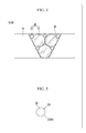
- FIG. 4 is a view illustrating a state in which particles with different sizes are injected in the particle injecting step in the method for manufacturing nanoholes shown in FIG. 1 .
- nanoholes 30 having a constant size that is smaller than the diameter of the injected particles 20 can be manufactured.
- nanoholes 30 with a user-desired size can be manufactured by selecting the size of injected particles 20
- the particles injected in the particle injecting step S120 may be a plurality of kinds of particles with different sizes.
- first particles 21 and second particles 22 having a smaller diameter than the first particles 21 may be simultaneously or sequentially injected into the through-hole 11.
- the second particles 22 are disposed in pores formed in a state in which the first particles 21 are arranged, and thus nanoholes 30 with a more minute scale can be formed when compared with the case in which only the first particles are injected.
- the present embodiment exemplifies the provision of two kinds of particles, that is, the first particles 21 and the second particles 22 having different sizes, but it is not limited thereto, and thus more minute nanoholes 30 can be manufactured by using two or more kinds of particles.
- the nanoholes 30 formed in the first embodiment of the present invention may have a pico-scale size.
- the particles injected in the particle injecting step S120 may be electrically or chemically treated particles. That is, particles that are surface-functionalized by an electrical or chemical treatment may be injected into the through-hole 11.
- the surfaces of the particles 20 may be positively charged using a peptide. That is, the peptide may bind to the surfaces of the particles 20 by providing a functional group, such as a hydroxyl group (OH) or a carboxyl group (COOH), to the surfaces of the particles 20.
- a functional group such as a hydroxyl group (OH) or a carboxyl group (COOH)
- FIG. 5 is a view schematically showing the binding of a functional group to a particle surface in the particle injecting step in the method for manufacturing nanoholes shown in FIG. 1 .
- Such a peptide has electrically positive (+) polarity since hydrogen is separated from a functional group, such as a hydroxyl group (OH) or a carboxyl group (COOH), and thus can limit the kind of particles which can pass through nanoholes 30.
- a functional group such as a hydroxyl group (OH) or a carboxyl group (COOH)
- the particles 20 may be injected into the through-hole 11 while the particles are charged, so that an electrically charged electric double layer is formed on surfaces of the particles.
- FIG. 6 is a view schematically showing a state in which an electric double layer is formed by injecting charged particles in the particle injecting step in the method for manufacturing nanoholes shown in FIG. 1 .
- the term electric double layer refers to a phenomenon in which charges are naturally formed along the particle, and a phenomenon in which charges having opposite polarity to charges formed on the particle form a layer around the charge.
- a layer having negative (-) polarity is formed around the particle 20.
- electrically negative (-) particles have limitations in passing through the nanohole 30, and only electrically positive (+) or neutral particles can pass through the nanohole 30.
- the particles 20 are surface-functionalized through an electric or chemical treatment, but is not limited thereto, and thus the conventionally known various methods can be utilized.
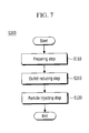
- FIG. 7 is a process flowchart schematically showing a method for manufacturing nanoholes according a second embodiment of the present invention.
- the method S200 for manufacturing nanoholes according to the second embodiment of the present invention, particles with a smaller size than a nano- or micro-scale through-hole 11 are injected into the through-hole 11, and as a result, nanoholes 30 with a size of several nanometers or smaller can be manufactured, wherein the method includes a preparing step S110, an inlet reducing step S215, and a particle injecting step S120.
- the present embodiment is different from the first embodiment in that a body 10 including a through-hole 11 of which an inlet 11 a and an outlet 11 b are symmetric to each other is utilized.
- the body 10 of the second embodiment includes the through-hole 11 having a structure in which the shape of the inlet 11 a and the shape of the outlet 11 b correspond to each other by forming the inlet 11 a and the outlet 11 b to have the same diameter.
- the through-hole 11 may be formed such that the diameter of the inlet 11 a and the diameter of the outlet 11 b are the same, and more preferably, the center of the inlet 11 a and the center of the outlet 11 b are on the same central axis.
- particles 20 injected in the below-describing particle injecting step (S120) can naturally leave through the outlet 11 b.
- FIG. 8 is a view schematically illustrating an outlet reduction step in the method for manufacturing nanoholes shown in FIG. 7 .
- an outlet reducing member 12 for shielding a part of the outlet 11 b is provided on a surface of the body in which the outlet 11 b is formed, in order to prevent the particles from leaving through the outlet 11 b.
- the outlet reducing member 12 having a penetration hole formed on an external surface thereof is attached to the surface of the body 10 in which the outlet 11 b is formed.
- the size of the penetration hole of the outlet reducing member 12 may be similar to or smaller than that of the outlet 11 b. That is, the outlet reducing member 12 is attached to the surface of the body 10 in which the outlet 11 b is formed, thereby shielding a part of the outlet 11 b. Therefore, the outlet reducing member 12 prevents the particles 20 from passing through the outlet 11 b and leaving the through-hole 11.
- the size of the outlet 11 b can be reduced by disposing the penetration hole of the outlet reducing member 12 and the outlet 11 b to be oblique to each other, that is, partially overlapping the outlet 11 b and a region of the outlet reducing member 12 in which the penetration hole is not formed.
- the outlet reducing step S215 according to the second embodiment of the present invention may be performed as long as a predetermined material is bonded on the edge of the outlet 11 b or the size of the outlet 11 b is reduced by any other method.
- FIG. 9 is a view schematically showing a filter according to an embodiment of the present invention.
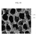
- FIG. 10 is an image showing an enlarged external surface of anodic aluminum oxide used as a filter part of the filter shown in FIG. 9 .
- a filter 300 according to an embodiment of the present invention has nanoholes manufactured by the method for manufacturing nanoholes according to the above-described first or second embodiment, and includes a filter part 310 and particles 320.
- the filter part 310 has a plurality of through-holes 311 passing through external surfaces thereof, contaminants are filtered by the through-holes 311, and thus purified air can be exhausted.
- the through-holes 311 have a scale of tens to hundreds of nanometers, and can filter minute particles with a larger scale than the through-holes 311.
- the filter part 310 may be prepared by an anodic aluminum oxidation filter.
- an inlet 311 a and an outlet 311 b of the through-hole 311 are asymmetric, and thus even though particles 320 are injected through the inlet 311 a, the particles 320 do not leave through the outlet 311 b due to the structural characteristics of the through-hole 311.
- a through-hole 311 having a symmetric structure as described in the methods (S100 and S200) for manufacturing nanoholes according to the first and second embodiments may be used.
- the particles 320 are inserted into the through-hole 311 to reduce the scale of the through-hole 311 to the several nano-scales or pico-scales. As described in the methods S100 and S200 for manufacturing nanoholes according to the first and second embodiments, a part of the through-hole 311 is shielded by the particles 310 placed inside the through-hole 311, and thus nanoholes 330 having a smaller scale than the through-hole 311 are manufactured.
- the particles may be placed inside the through-hole 311 while being surface-functionalized, and this feature is substantially the same as those in the methods S100 and S200 for manufacturing nanoholes according to the first and second embodiments, and thus a detailed description thereof will be omitted.
- the particles 320 have electrically positive (+) or negative (-) polarity by an electrical or chemical treatment, and thus the filter part 310 can selectively pass through only predetermined materials in air.
Landscapes
- Chemical & Material Sciences (AREA)
- Chemical Kinetics & Catalysis (AREA)
- Organic Chemistry (AREA)
- Inorganic Chemistry (AREA)
- Engineering & Computer Science (AREA)
- Electrochemistry (AREA)
- Materials Engineering (AREA)
- Metallurgy (AREA)
- Manufacturing & Machinery (AREA)
- Filtering Materials (AREA)
- Physical Or Chemical Processes And Apparatus (AREA)
Abstract
Description
- The present invention relates to a method for manufacturing nanoholes and a filter manufactured by the same, and more particularly, to a method for manufacturing nanoholes, the method being capable of easily manufacturing nanoholes with a size of several to hundreds of nanometers, and to a filter manufactured by the same.
- A nanohole refers to a pore or passage having a nanoscale width, and is used in various fields, such as for a computing device and a memory device.
- It has been reported until now that such nanoholes are arranged by colloidal lithographic etching, nanoimprint lithography, the use of an anodic aluminum oxide template, and block copolymer-based optical lithographic patterning processes.
- However, such methods employ separate apparatuses or methods enabling nanoscale patterning, and thus have problems of requiring a lot of time and complicated processes, and there are technical and commercial limitations in manufacturing nanoholes with a diameter of 20 nm or smaller.
- For example, in cases where nanoholes are manufactured through mechanical processing, the sizes of tools are restricted, and in cases of photolithography, the shape limit of a photosensitive film is at least 1 µm due to optical diffraction of a photo-mask. Therefore, it is, in fact, difficult to realize several nanometer-sized nanoholes through the above techniques.
- Moreover, when a filter capable of collecting nanoscale particles is manufactured, current techniques enable the manufacture of holes of tens of nanometers, but it is difficult to manufacture filters having holes with a size of below such sizes, that is, of several nanometers.
- <Related cited document 1> Korean Patent Registration No.
10-1408194 - <Related cited document 2> Korean Patent Registration No.
10-10-1399459 - The above information disclosed in this Background section is only for enhancement of understanding of the background of the invention and therefore it may contain information that does not form the prior art that is already known in this country to a person of ordinary skill in the art.
- The present invention has been made in an effort to provide a method for manufacturing nanoholes and a filter manufactured by the same, having advantages of easily and simply manufacturing nanoholes with a scale of several nanometers or less.
- An exemplary embodiment of the present invention provides a method for manufacturing nanoholes, the method including: a preparing step of preparing a body having a through-hole which passes through two facing surfaces and has a nano- or micro-scale diameter; and a particle injecting step of injecting particles with a smaller diameter than the through-hole into the through-hole to form nanoholes with a smaller scale than the through-hole.
- In the particle injecting step, a plurality of kinds of particles with different sizes may be injected into the through-hole.
- In the particle injecting step, the same kind of particles with the same size may be injected into the through-hole.
- In the particle injecting step, electrically or chemically treated particles may be injected.
- An inlet, through which the particles are injected in the particle injecting step, and an outlet, which is opposite to the inlet, may be formed in an asymmetric structure so that the particles injected in the particle injecting step do not leave the through-hole.
- In the through-hole, the diameter of the inlet may be larger than that of the outlet.
- An inlet, to which the particles are injected in the particle injecting step, and an outlet, which is opposite to the inlet, may be formed in a symmetric structure, and the method may further include an outlet reducing step of reducing the diameter of the outlet of the through-hole, between the preparing step and the particle injecting step.
- Another embodiment of the present invention provides a filter including: a filter part having a through-hole which penetrates two facing surfaces and has a nano- or micro-scale diameter; and particles inserted into the through-hole and having a smaller diameter than the through-hole, wherein the filter part has nanoholes with a smaller scale than the through-hole by the particles injected into the through-hole.
- The size of the nanoholes may be controlled by adjusting the size of particles injected into the through-hole.
- The particles may have electrically positive or negative polarity by binding to a functional group.
- A surface of the particles may be positively or negatively charged so that an electrically charged electric double layer is formed on the surface of the particle or a region adjacent to the surface.
- In the through-hole, the diameter of an inlet, through which the particles are injected, may be larger than that of an outlet, which is opposite to the inlet.
- The filter part may be an anodic aluminum oxide (AAO) membrane.
- According to an embodiment of the present invention, a method for manufacturing nanoholes can be provided, the method being capable of easily manufacturing nanoholes with a scale of several nanometers or less.
- Furthermore, the size and arrangement of nanoholes can be controlled by adjusting the size of injected particles.
- In addition, surface-functionalized nanoholes can be manufactured by performing a chemical or electric treatment on injected particles.
- According to an embodiment of the present invention, a filter capable of easily collecting particles even with a size of several nanometers can be provided.
- Furthermore, even particles with a smaller size than nanoholes can be easily collected by surface-functionalizing particles injected in the nanoholes.
-
-
FIG. 1 is a process flowchart schematically showing a method for manufacturing nanoholes according a first embodiment of the present invention; -
FIG. 2 is a front view schematically illustrating a preparing step in the method for manufacturing nanoholes shown inFIG. 1 ; -
FIG. 3 is a view illustrating a state in which particles with the same size are injected in the particle injecting step in the method for manufacturing nanoholes shown inFIG. 1 ; -
FIG. 4 is a view illustrating a state in which particles with different sizes are injected in the particle injecting step in the method for manufacturing nanoholes shown inFIG. 1 ; -
FIG. 5 is a view schematically showing the binding of a functional group to a particle surface in the particle injecting step in the method for manufacturing nanoholes shown inFIG. 1 ; -
FIG. 6 is a view schematically showing a state in which an electric double layer is formed by injecting charged particles in the particle injecting step in the method for manufacturing nanoholes shown inFIG. 1 ; -
FIG. 7 is a process flowchart schematically showing a method for manufacturing nanoholes according a second embodiment of the present invention; -
FIG. 8 is a view schematically illustrating an outlet reducing step in the method for manufacturing nanoholes shown inFIG. 7 ; -
FIG. 9 is a view schematically showing a filter according to an embodiment of the present invention; and -
FIG. 10 is an image showing an enlarged external surface of anodic aluminum oxide used as a filter part of the filter shown inFIG. 9 . - The present invention will be described more fully hereinafter with reference to the accompanying drawings, in which embodiments of the invention are shown. As those skilled in the art would realize, the described embodiments may be modified in various different ways, all without departing from the spirit or scope of the present invention. The drawings and description are to be regarded as illustrative in nature and not restrictive. Like reference numerals designate like elements throughout the specification.
- Prior to descriptions, in the embodiments, elements having the same configuration are denoted by the same reference numerals and will be described representatively in a first embodiment, and only configurations different from those of the first embodiment will be described in the other embodiments.
- Hereinafter, a method S100 for manufacturing nanoholes according to a first embodiment of the present invention will be described with reference to the accompanying drawings.
-
FIG. 1 is a process flowchart schematically showing a method for manufacturing nanoholes according a first embodiment of the present invention. - Referring to
FIG. 1 , according to the method S100 for manufacturing nanoholes according to the first embodiment of the present invention, particles with a smaller size than a nano- or micro-scale through-hole 11 are injected into the through-hole 11, and as a result,nanoholes 30 with a size of several nanometers or smaller can be manufactured, wherein the method comprises a preparing step S110 and a particle injecting step S120. -
FIG. 2 is a front view schematically illustrating a preparing step in the method for manufacturing nanoholes shown inFIG. 1 . - Referring to
FIG. 2 , in the preparing step S110, abody 10 which passes through two facing surfaces and has a through-hole 11 with a nano- or micro-scale diameter is prepared. - Here, the through-
hole 11 may be formed to pass through upper and lower surfaces of thebody 10, or right and left surfaces of thebody 10. - In the first embodiment of the present invention, the through-
hole 11 is prepared such that, based on a direction in whichparticles 20 are injected in the below-described particle injecting step S120, aninlet 11 a, through which theparticles 20 are injected, and anoutlet 11 b, which is opposite to theinlet 11 a, are asymmetric. - More specifically, the shape of the
inlet 11 a and the shape of theoutlet 11 b may be asymmetric to each other by differently preparing the diameter of theinlet 11 a and the diameter of theoutlet 11 b. - That is, the diameter of the
inlet 11 a and the diameter of theoutlet 11 b are differently prepared, and more preferably, the diameter of theinlet 11 a is prepared to be larger than the diameter of theoutlet 11 b, thereby preventing theparticles 20 injected in the particle injecting step S120 from leaving through theoutlet 11 b. - Here, the diameter of the
outlet 11 b may be preferably smaller than the diameter of theparticles 20 injected in the below-described particle injecting step S120, but is not limited thereto. - In the particle injecting step S120, particles with a smaller diameter than the through-
hole 11 are injected into the through-hole 11, thereby manufacturing nanoholes with a smaller scale than the through-hole 11. - That is, the
particles 20 are injected into the through-hole 11, and thusnanoholes 30 are manufactured by pores formed between theparticles 20. - Here,
nanoholes 30 with a user-desired size can be manufactured by selecting the kind of injectedparticles 20. -
FIG. 3 is a view illustrating a state in which particles with the same size are injected in the particle injecting step in the method for manufacturing nanoholes shown inFIG. 1 , andFIG. 4 is a view illustrating a state in which particles with different sizes are injected in the particle injecting step in the method for manufacturing nanoholes shown inFIG. 1 . - For example, as shown in
FIG. 3 , when it is assumed that theparticles 20 injected into the through-hole 11 have the same size,nanoholes 30 having a constant size that is smaller than the diameter of the injectedparticles 20 can be manufactured. - That, when it is assumed that the
particles 20 have a completely circular shape,nanoholes 30 with a user-desired size can be manufactured by selecting the size of injectedparticles 20 - According to the first embodiment of the present invention, the particles injected in the particle injecting step S120 may be a plurality of kinds of particles with different sizes.
- For example, as shown in
FIG. 4 ,first particles 21 andsecond particles 22 having a smaller diameter than thefirst particles 21 may be simultaneously or sequentially injected into the through-hole 11. As such, when thefirst particles 21 and thesecond particles 22 are injected into the through-hole 11, thesecond particles 22 are disposed in pores formed in a state in which thefirst particles 21 are arranged, and thus nanoholes 30 with a more minute scale can be formed when compared with the case in which only the first particles are injected. - Here, for the convenience of description, the present embodiment exemplifies the provision of two kinds of particles, that is, the
first particles 21 and thesecond particles 22 having different sizes, but it is not limited thereto, and thus moreminute nanoholes 30 can be manufactured by using two or more kinds of particles. - Further, when the injected
particles 20 are several nanometer-level nanoparticles, thenanoholes 30 formed in the first embodiment of the present invention may have a pico-scale size. - According to the first embodiment of the present invention, the particles injected in the particle injecting step S120 may be electrically or chemically treated particles. That is, particles that are surface-functionalized by an electrical or chemical treatment may be injected into the through-
hole 11. - Here, for the particles that are surface-functionalized by an electrical or chemical treatment, several methods that are conventionally disclosed may be utilized.
- As one example of the chemical treatment, the surfaces of the
particles 20 may be positively charged using a peptide. That is, the peptide may bind to the surfaces of theparticles 20 by providing a functional group, such as a hydroxyl group (OH) or a carboxyl group (COOH), to the surfaces of theparticles 20. -
FIG. 5 is a view schematically showing the binding of a functional group to a particle surface in the particle injecting step in the method for manufacturing nanoholes shown inFIG. 1 . - Such a peptide has electrically positive (+) polarity since hydrogen is separated from a functional group, such as a hydroxyl group (OH) or a carboxyl group (COOH), and thus can limit the kind of particles which can pass through
nanoholes 30. - As one example of the electrical treatment, the
particles 20 may be injected into the through-hole 11 while the particles are charged, so that an electrically charged electric double layer is formed on surfaces of the particles. -
FIG. 6 is a view schematically showing a state in which an electric double layer is formed by injecting charged particles in the particle injecting step in the method for manufacturing nanoholes shown inFIG. 1 . - Referring to
FIG. 6 , the term electric double layer refers to a phenomenon in which charges are naturally formed along the particle, and a phenomenon in which charges having opposite polarity to charges formed on the particle form a layer around the charge. For example, when the surface of theparticle 20 is positively (+) charged, a layer having negative (-) polarity is formed around theparticle 20. - Thus, electrically negative (-) particles have limitations in passing through the
nanohole 30, and only electrically positive (+) or neutral particles can pass through thenanohole 30. - The above-described embodiment exemplifies that the
particles 20 are surface-functionalized through an electric or chemical treatment, but is not limited thereto, and thus the conventionally known various methods can be utilized. - Next, a method S200 for manufacturing nanoholes according to a second embodiment of the present invention will be described.
-
FIG. 7 is a process flowchart schematically showing a method for manufacturing nanoholes according a second embodiment of the present invention. - Referring to
FIG. 7 , in the method S200 for manufacturing nanoholes according to the second embodiment of the present invention, particles with a smaller size than a nano- or micro-scale through-hole 11 are injected into the through-hole 11, and as a result, nanoholes 30 with a size of several nanometers or smaller can be manufactured, wherein the method includes a preparing step S110, an inlet reducing step S215, and a particle injecting step S120. - Since the preparing step S110 is substantially the same as that in the first embodiment, a description thereof will be omitted.
- However, the present embodiment is different from the first embodiment in that a
body 10 including a through-hole 11 of which aninlet 11 a and anoutlet 11 b are symmetric to each other is utilized. - More specifically, the
body 10 of the second embodiment includes the through-hole 11 having a structure in which the shape of theinlet 11 a and the shape of theoutlet 11 b correspond to each other by forming theinlet 11 a and theoutlet 11 b to have the same diameter. - Further, the through-
hole 11 may be formed such that the diameter of theinlet 11 a and the diameter of theoutlet 11 b are the same, and more preferably, the center of theinlet 11 a and the center of theoutlet 11 b are on the same central axis. - However, according to such a structure,
particles 20 injected in the below-describing particle injecting step (S120) can naturally leave through theoutlet 11 b. -
FIG. 8 is a view schematically illustrating an outlet reduction step in the method for manufacturing nanoholes shown inFIG. 7 . - Referring to
FIG. 8 , in the outlet reducing step S215, as described above, in cases where the through-hole 11 has a symmetric structure, anoutlet reducing member 12 for shielding a part of theoutlet 11 b is provided on a surface of the body in which theoutlet 11 b is formed, in order to prevent the particles from leaving through theoutlet 11 b. - According to the second embodiment of the present invention, in the outlet reducing step S215, the
outlet reducing member 12 having a penetration hole formed on an external surface thereof is attached to the surface of thebody 10 in which theoutlet 11 b is formed. - Here, the size of the penetration hole of the
outlet reducing member 12 may be similar to or smaller than that of theoutlet 11 b. That is, theoutlet reducing member 12 is attached to the surface of thebody 10 in which theoutlet 11 b is formed, thereby shielding a part of theoutlet 11 b. Therefore, theoutlet reducing member 12 prevents theparticles 20 from passing through theoutlet 11 b and leaving the through-hole 11. - That is, without being limited thereto, if the penetration hole of the
outlet reducing member 12 has a larger size than theoutlet 11 b, the size of theoutlet 11 b can be reduced by disposing the penetration hole of theoutlet reducing member 12 and theoutlet 11 b to be oblique to each other, that is, partially overlapping theoutlet 11 b and a region of theoutlet reducing member 12 in which the penetration hole is not formed. - However, the reducing of the size of the outlet is not limited to the above methods. The outlet reducing step S215 according to the second embodiment of the present invention may be performed as long as a predetermined material is bonded on the edge of the
outlet 11 b or the size of theoutlet 11 b is reduced by any other method. - Since the particle injecting step S120 is substantially the same as that in the first embodiment, a description thereof will be omitted.
- Next, a
filter 300 according to an embodiment of the present invention will be described. -
FIG. 9 is a view schematically showing a filter according to an embodiment of the present invention. -
FIG. 10 is an image showing an enlarged external surface of anodic aluminum oxide used as a filter part of the filter shown inFIG. 9 . - Referring to
FIG. 9 , afilter 300 according to an embodiment of the present invention has nanoholes manufactured by the method for manufacturing nanoholes according to the above-described first or second embodiment, and includes afilter part 310 andparticles 320. - Referring to
FIG. 10 , thefilter part 310 has a plurality of through-holes 311 passing through external surfaces thereof, contaminants are filtered by the through-holes 311, and thus purified air can be exhausted. - Here, the through-
holes 311 have a scale of tens to hundreds of nanometers, and can filter minute particles with a larger scale than the through-holes 311. - Referring to
FIG. 10 , according to an embodiment of the present invention, thefilter part 310 may be prepared by an anodic aluminum oxidation filter. Here, in the anodic aluminum oxide filter, aninlet 311 a and anoutlet 311 b of the through-hole 311 are asymmetric, and thus even thoughparticles 320 are injected through theinlet 311 a, theparticles 320 do not leave through theoutlet 311 b due to the structural characteristics of the through-hole 311. - Without being limited to, a through-
hole 311 having a symmetric structure as described in the methods (S100 and S200) for manufacturing nanoholes according to the first and second embodiments may be used. - The
particles 320 are inserted into the through-hole 311 to reduce the scale of the through-hole 311 to the several nano-scales or pico-scales. As described in the methods S100 and S200 for manufacturing nanoholes according to the first and second embodiments, a part of the through-hole 311 is shielded by theparticles 310 placed inside the through-hole 311, and thus nanoholes 330 having a smaller scale than the through-hole 311 are manufactured. - Here, the particles may be placed inside the through-
hole 311 while being surface-functionalized, and this feature is substantially the same as those in the methods S100 and S200 for manufacturing nanoholes according to the first and second embodiments, and thus a detailed description thereof will be omitted. - However, as for the functional effect thereof, the
particles 320 have electrically positive (+) or negative (-) polarity by an electrical or chemical treatment, and thus thefilter part 310 can selectively pass through only predetermined materials in air. - While this invention has been described in connection with what is presently considered to be practical exemplary embodiments, it is to be understood that the invention is not limited to the disclosed embodiments, but, on the contrary, is intended to cover various modifications and equivalent arrangements included within the scope of the appended claims.
| 10: | body | 20: | particle |
| S100: | nanohole preparing step | S110: | preparing step |
| S120: | particle injecting step | ||
| S200: | nanohole preparing step | S215: | outlet reducing step |
| 300: | filter | 310: | filter part |
| 320: | particle |
Claims (13)
- A method for manufacturing nanoholes, the method comprising:a preparing step of preparing a body having a through-hole which passes through two facing surfaces and has a nano- or micro-scale diameter; anda particle injecting step of injecting particles with a smaller diameter than the through-hole into the through-hole to form nanoholes with a smaller scale than the through-hole.
- The method of claim 1, wherein in the particle injecting step, a plurality of kinds of particles with different sizes are injected into the through-hole.
- The method of claim 1, wherein in the particle injecting step, the same kind of particles with the same size are injected into the through-hole.
- The method of claim 1, wherein in the particle injecting step, electrically or chemically treated particles are injected.
- The method of any one of claims 1 to 4, wherein an inlet, through which the particles are injected in the particle injecting step, and an outlet, which is opposite to the inlet, are formed in an asymmetric structure so that the particles injected in the particle injecting step do not leave the through-hole.
- The method of claim 5, wherein in the through-hole, the diameter of the inlet is larger than that of the outlet.
- The method of any one of claims 1 to 4, wherein an inlet, to which the particles are injected in the particle injecting step, and an outlet, which is opposite to the inlet, are formed in a symmetric structure, and
wherein the method further comprises an outlet reducing step of reducing the diameter of the outlet of the through-hole, between the preparing step and the particle injecting step. - A filter comprising:a filter part having a through-hole which penetrates two facing surfaces and has a nano- or micro-scale diameter; andparticles inserted into the through-hole and having a smaller diameter than the through-hole,wherein the filter part has nanoholes with a smaller scale than the through-hole by the particles injected into the through-hole.
- The filter of claim 8, wherein the size of the nanoholes is controlled by adjusting the size of particles injected into the through-hole.
- The filter of claim 8, wherein the particles have electrically positive or negative polarity by binding to a functional group.
- The filter of claim 8, wherein a surface of the particles is positively or negatively charged so that an electrically charged electric double layer is formed on the surface of the particle or a region adjacent to the surface.
- The filter of any one of claims 1 to 11, wherein in the through-hole, the diameter of an inlet, through which the particles are injected, is larger than that of an outlet, which is opposite to the inlet.
- The filter of claim 12, wherein the filter part is an anodic aluminum oxide (AAO) membrane.
Applications Claiming Priority (1)
| Application Number | Priority Date | Filing Date | Title |
|---|---|---|---|
| KR1020140121300A KR101605632B1 (en) | 2014-09-12 | 2014-09-12 | Method for manufacturing nano hole and filter manufactured by the same |
Publications (2)
| Publication Number | Publication Date |
|---|---|
| EP2995368A1 true EP2995368A1 (en) | 2016-03-16 |
| EP2995368B1 EP2995368B1 (en) | 2020-08-19 |
Family
ID=52432720
Family Applications (1)
| Application Number | Title | Priority Date | Filing Date |
|---|---|---|---|
| EP15153186.0A Active EP2995368B1 (en) | 2014-09-12 | 2015-01-30 | Method for manufacturing nanoholes and filter manufactured by the same |
Country Status (3)
| Country | Link |
|---|---|
| EP (1) | EP2995368B1 (en) |
| KR (1) | KR101605632B1 (en) |
| SG (1) | SG10201500789XA (en) |
Cited By (9)
| Publication number | Priority date | Publication date | Assignee | Title |
|---|---|---|---|---|
| WO2017023380A1 (en) | 2015-08-05 | 2017-02-09 | Lockheed Martin Corporation | Two-dimensional materials and uses thereof |
| EP3331588A4 (en) * | 2015-08-05 | 2019-04-03 | Lockheed Martin Corporation | Two-dimensional materials and uses thereof |
| US10418143B2 (en) | 2015-08-05 | 2019-09-17 | Lockheed Martin Corporation | Perforatable sheets of graphene-based material |
| US10471199B2 (en) | 2013-06-21 | 2019-11-12 | Lockheed Martin Corporation | Graphene-based filter for isolating a substance from blood |
| US10500546B2 (en) | 2014-01-31 | 2019-12-10 | Lockheed Martin Corporation | Processes for forming composite structures with a two-dimensional material using a porous, non-sacrificial supporting layer |
| US10653824B2 (en) | 2012-05-25 | 2020-05-19 | Lockheed Martin Corporation | Two-dimensional materials and uses thereof |
| US10696554B2 (en) | 2015-08-06 | 2020-06-30 | Lockheed Martin Corporation | Nanoparticle modification and perforation of graphene |
| US10981120B2 (en) | 2016-04-14 | 2021-04-20 | Lockheed Martin Corporation | Selective interfacial mitigation of graphene defects |
| US10980919B2 (en) | 2016-04-14 | 2021-04-20 | Lockheed Martin Corporation | Methods for in vivo and in vitro use of graphene and other two-dimensional materials |
Families Citing this family (2)
| Publication number | Priority date | Publication date | Assignee | Title |
|---|---|---|---|---|
| KR101930068B1 (en) | 2017-04-03 | 2018-12-17 | 한국기계연구원 | Membrane Filter for Detecting Target Particle, Method for Manufacturing the Same, and Method for Detecting Target Particle Using the Same |
| KR101980244B1 (en) * | 2017-11-15 | 2019-08-28 | 한국기계연구원 | Omni membrane for phase separation and method for making the same omni membrane |
Citations (8)
| Publication number | Priority date | Publication date | Assignee | Title |
|---|---|---|---|---|
| US3022187A (en) * | 1958-02-24 | 1962-02-20 | Commissariat Energie Atomique | Porous membranes of very fine porosity and proceses for production thereof |
| JPS6414875A (en) * | 1987-07-08 | 1989-01-19 | Yamaha Motor Co Ltd | Separator for fuel cell |
| US6613241B1 (en) * | 1999-10-29 | 2003-09-02 | California Insitute Of Technology | MEMS elements with integrated porous membranes and method of making the same |
| JP2005144363A (en) * | 2003-11-17 | 2005-06-09 | Nissan Motor Co Ltd | Hydrogen separation membrane structure and method for producing the same |
| US20080006574A1 (en) * | 2006-07-05 | 2008-01-10 | General Electric Company | Membrane structure and method of making |
| JP2008027676A (en) * | 2006-07-19 | 2008-02-07 | Tokai Rubber Ind Ltd | Method for manufacturing anisotropic conductive film and anisotropic conductive film |
| KR101408194B1 (en) | 2013-10-14 | 2014-06-17 | 한국기계연구원 | Manufacturing method of nano channel |
| KR101399459B1 (en) | 2012-11-28 | 2014-06-27 | 한국기계연구원 | Fabrication method for nano-hole using compressing process |
Family Cites Families (2)
| Publication number | Priority date | Publication date | Assignee | Title |
|---|---|---|---|---|
| EP2183383B1 (en) | 2007-08-01 | 2013-01-16 | Hitachi Chemical Co., Ltd. | Pathogen detection in large-volume particulate samples |
| KR101656846B1 (en) | 2008-12-23 | 2016-09-12 | 미카티스 엔브이 | Assay device and method for performing biological assays |
-
2014
- 2014-09-12 KR KR1020140121300A patent/KR101605632B1/en active Active
-
2015
- 2015-01-30 EP EP15153186.0A patent/EP2995368B1/en active Active
- 2015-02-02 SG SG10201500789XA patent/SG10201500789XA/en unknown
Patent Citations (8)
| Publication number | Priority date | Publication date | Assignee | Title |
|---|---|---|---|---|
| US3022187A (en) * | 1958-02-24 | 1962-02-20 | Commissariat Energie Atomique | Porous membranes of very fine porosity and proceses for production thereof |
| JPS6414875A (en) * | 1987-07-08 | 1989-01-19 | Yamaha Motor Co Ltd | Separator for fuel cell |
| US6613241B1 (en) * | 1999-10-29 | 2003-09-02 | California Insitute Of Technology | MEMS elements with integrated porous membranes and method of making the same |
| JP2005144363A (en) * | 2003-11-17 | 2005-06-09 | Nissan Motor Co Ltd | Hydrogen separation membrane structure and method for producing the same |
| US20080006574A1 (en) * | 2006-07-05 | 2008-01-10 | General Electric Company | Membrane structure and method of making |
| JP2008027676A (en) * | 2006-07-19 | 2008-02-07 | Tokai Rubber Ind Ltd | Method for manufacturing anisotropic conductive film and anisotropic conductive film |
| KR101399459B1 (en) | 2012-11-28 | 2014-06-27 | 한국기계연구원 | Fabrication method for nano-hole using compressing process |
| KR101408194B1 (en) | 2013-10-14 | 2014-06-17 | 한국기계연구원 | Manufacturing method of nano channel |
Cited By (9)
| Publication number | Priority date | Publication date | Assignee | Title |
|---|---|---|---|---|
| US10653824B2 (en) | 2012-05-25 | 2020-05-19 | Lockheed Martin Corporation | Two-dimensional materials and uses thereof |
| US10471199B2 (en) | 2013-06-21 | 2019-11-12 | Lockheed Martin Corporation | Graphene-based filter for isolating a substance from blood |
| US10500546B2 (en) | 2014-01-31 | 2019-12-10 | Lockheed Martin Corporation | Processes for forming composite structures with a two-dimensional material using a porous, non-sacrificial supporting layer |
| WO2017023380A1 (en) | 2015-08-05 | 2017-02-09 | Lockheed Martin Corporation | Two-dimensional materials and uses thereof |
| EP3331588A4 (en) * | 2015-08-05 | 2019-04-03 | Lockheed Martin Corporation | Two-dimensional materials and uses thereof |
| US10418143B2 (en) | 2015-08-05 | 2019-09-17 | Lockheed Martin Corporation | Perforatable sheets of graphene-based material |
| US10696554B2 (en) | 2015-08-06 | 2020-06-30 | Lockheed Martin Corporation | Nanoparticle modification and perforation of graphene |
| US10981120B2 (en) | 2016-04-14 | 2021-04-20 | Lockheed Martin Corporation | Selective interfacial mitigation of graphene defects |
| US10980919B2 (en) | 2016-04-14 | 2021-04-20 | Lockheed Martin Corporation | Methods for in vivo and in vitro use of graphene and other two-dimensional materials |
Also Published As
| Publication number | Publication date |
|---|---|
| KR101605632B1 (en) | 2016-03-23 |
| EP2995368B1 (en) | 2020-08-19 |
| SG10201500789XA (en) | 2016-04-28 |
Similar Documents
| Publication | Publication Date | Title |
|---|---|---|
| EP2995368B1 (en) | Method for manufacturing nanoholes and filter manufactured by the same | |
| Li et al. | Self-driven magnetorobots for recyclable and scalable micro/nanoplastic removal from nonmarine waters | |
| DE102008060644B4 (en) | Process for producing a graphane nanostructure | |
| DE112017001898B4 (en) | Method for influencing and capturing particles in microfluidic units using two-dimensional materials and corresponding device | |
| Duong et al. | Enhanced magnetism in highly ordered magnetite nanoparticle‐filled nanohole arrays | |
| DE112009001476T5 (en) | Process for producing semiconductor structures and semiconductor structures obtained by such processes | |
| Guo et al. | Nanopore and nanobushing arrays from ABC triblock thin films containing two etchable blocks | |
| DE102016216925A1 (en) | Micromechanical device and method for two-dimensionally deflecting light | |
| JP2019517909A (en) | Two-dimensional membrane structure having a flow path | |
| US20130011799A1 (en) | Method for the production of polymeric membranes having an ordered arrangement of high-aspect-ratio nanopores, by means of heavy ion bombing | |
| DE102008039798A1 (en) | Method of transferring nanostructures into a substrate | |
| KR101980244B1 (en) | Omni membrane for phase separation and method for making the same omni membrane | |
| DE112013003351T5 (en) | magnetic sensor | |
| KR101202017B1 (en) | Method for manufacturing Ag nano-wire by using plasma sputtering | |
| Mohamed-Noriega et al. | Coating of NIL printed polymeric templates with semiconductor nanoparticles in solution for the preparation of anisotropic inorganic structures | |
| DE102013203056A1 (en) | Method of making a microsieve | |
| WO2019214863A1 (en) | Method for producing an atom trap, and atom trap | |
| DE102015004887A1 (en) | Apparatus and method for cleaning and increasing the concentration of magnetic particles in a dispersion | |
| DE202013105600U1 (en) | Object-holding-and-alignment device, device for aligning an object and a mask to each other and vacuum chamber with one of these two devices | |
| DE102013200354A1 (en) | Method and apparatus for producing a multilayer electrode system | |
| DE102014203075A1 (en) | Magnetic sensor and method for its manufacture | |
| Gunawan et al. | One-dimensional fossil-like γ-Fe2O3@ carbon nanostructure: preparation, structural characterization and application as adsorbent for fast and selective recovery of gold ions from aqueous solution | |
| JP4877806B2 (en) | Polymer multi-stage nanowire and starburst type nanoparticle and production method thereof | |
| KR20200077999A (en) | Method for Manufacturing Ultrafine Graphene Membrane Having Nano Pores | |
| US12427496B2 (en) | Preparing method of membrane filter including inverse opal structure |
Legal Events
| Date | Code | Title | Description |
|---|---|---|---|
| PUAI | Public reference made under article 153(3) epc to a published international application that has entered the european phase |
Free format text: ORIGINAL CODE: 0009012 |
|
| 17P | Request for examination filed |
Effective date: 20150130 |
|
| AK | Designated contracting states |
Kind code of ref document: A1 Designated state(s): AL AT BE BG CH CY CZ DE DK EE ES FI FR GB GR HR HU IE IS IT LI LT LU LV MC MK MT NL NO PL PT RO RS SE SI SK SM TR |
|
| AX | Request for extension of the european patent |
Extension state: BA ME |
|
| RBV | Designated contracting states (corrected) |
Designated state(s): AL AT BE BG CH CY CZ DE DK EE ES FI FR GB GR HR HU IE IS IT LI LT LU LV MC MK MT NL NO PL PT RO RS SE SI SK SM TR |
|
| STAA | Information on the status of an ep patent application or granted ep patent |
Free format text: STATUS: EXAMINATION IS IN PROGRESS |
|
| 17Q | First examination report despatched |
Effective date: 20170921 |
|
| GRAP | Despatch of communication of intention to grant a patent |
Free format text: ORIGINAL CODE: EPIDOSNIGR1 |
|
| STAA | Information on the status of an ep patent application or granted ep patent |
Free format text: STATUS: GRANT OF PATENT IS INTENDED |
|
| INTG | Intention to grant announced |
Effective date: 20200319 |
|
| GRAS | Grant fee paid |
Free format text: ORIGINAL CODE: EPIDOSNIGR3 |
|
| GRAA | (expected) grant |
Free format text: ORIGINAL CODE: 0009210 |
|
| STAA | Information on the status of an ep patent application or granted ep patent |
Free format text: STATUS: THE PATENT HAS BEEN GRANTED |
|
| AK | Designated contracting states |
Kind code of ref document: B1 Designated state(s): AL AT BE BG CH CY CZ DE DK EE ES FI FR GB GR HR HU IE IS IT LI LT LU LV MC MK MT NL NO PL PT RO RS SE SI SK SM TR |
|
| REG | Reference to a national code |
Ref country code: CH Ref legal event code: EP |
|
| REG | Reference to a national code |
Ref country code: DE Ref legal event code: R096 Ref document number: 602015057588 Country of ref document: DE |
|
| REG | Reference to a national code |
Ref country code: AT Ref legal event code: REF Ref document number: 1303315 Country of ref document: AT Kind code of ref document: T Effective date: 20200915 |
|
| REG | Reference to a national code |
Ref country code: IE Ref legal event code: FG4D |
|
| REG | Reference to a national code |
Ref country code: DE Ref legal event code: R081 Ref document number: 602015057588 Country of ref document: DE Owner name: KOREA INSTITUTE OF MACHINERY & MATERIALS, KR Free format text: FORMER OWNER: KOREA INSTITUTE OF MACHINERY & MATERIALS, DAJEON, KR |
|
| REG | Reference to a national code |
Ref country code: LT Ref legal event code: MG4D |
|
| REG | Reference to a national code |
Ref country code: NL Ref legal event code: MP Effective date: 20200819 |
|
| PG25 | Lapsed in a contracting state [announced via postgrant information from national office to epo] |
Ref country code: PT Free format text: LAPSE BECAUSE OF FAILURE TO SUBMIT A TRANSLATION OF THE DESCRIPTION OR TO PAY THE FEE WITHIN THE PRESCRIBED TIME-LIMIT Effective date: 20201221 Ref country code: NO Free format text: LAPSE BECAUSE OF FAILURE TO SUBMIT A TRANSLATION OF THE DESCRIPTION OR TO PAY THE FEE WITHIN THE PRESCRIBED TIME-LIMIT Effective date: 20201119 Ref country code: LT Free format text: LAPSE BECAUSE OF FAILURE TO SUBMIT A TRANSLATION OF THE DESCRIPTION OR TO PAY THE FEE WITHIN THE PRESCRIBED TIME-LIMIT Effective date: 20200819 Ref country code: FI Free format text: LAPSE BECAUSE OF FAILURE TO SUBMIT A TRANSLATION OF THE DESCRIPTION OR TO PAY THE FEE WITHIN THE PRESCRIBED TIME-LIMIT Effective date: 20200819 Ref country code: GR Free format text: LAPSE BECAUSE OF FAILURE TO SUBMIT A TRANSLATION OF THE DESCRIPTION OR TO PAY THE FEE WITHIN THE PRESCRIBED TIME-LIMIT Effective date: 20201120 Ref country code: HR Free format text: LAPSE BECAUSE OF FAILURE TO SUBMIT A TRANSLATION OF THE DESCRIPTION OR TO PAY THE FEE WITHIN THE PRESCRIBED TIME-LIMIT Effective date: 20200819 Ref country code: SE Free format text: LAPSE BECAUSE OF FAILURE TO SUBMIT A TRANSLATION OF THE DESCRIPTION OR TO PAY THE FEE WITHIN THE PRESCRIBED TIME-LIMIT Effective date: 20200819 Ref country code: BG Free format text: LAPSE BECAUSE OF FAILURE TO SUBMIT A TRANSLATION OF THE DESCRIPTION OR TO PAY THE FEE WITHIN THE PRESCRIBED TIME-LIMIT Effective date: 20201119 |
|
| REG | Reference to a national code |
Ref country code: AT Ref legal event code: MK05 Ref document number: 1303315 Country of ref document: AT Kind code of ref document: T Effective date: 20200819 |
|
| PG25 | Lapsed in a contracting state [announced via postgrant information from national office to epo] |
Ref country code: IS Free format text: LAPSE BECAUSE OF FAILURE TO SUBMIT A TRANSLATION OF THE DESCRIPTION OR TO PAY THE FEE WITHIN THE PRESCRIBED TIME-LIMIT Effective date: 20201219 Ref country code: LV Free format text: LAPSE BECAUSE OF FAILURE TO SUBMIT A TRANSLATION OF THE DESCRIPTION OR TO PAY THE FEE WITHIN THE PRESCRIBED TIME-LIMIT Effective date: 20200819 Ref country code: RS Free format text: LAPSE BECAUSE OF FAILURE TO SUBMIT A TRANSLATION OF THE DESCRIPTION OR TO PAY THE FEE WITHIN THE PRESCRIBED TIME-LIMIT Effective date: 20200819 Ref country code: PL Free format text: LAPSE BECAUSE OF FAILURE TO SUBMIT A TRANSLATION OF THE DESCRIPTION OR TO PAY THE FEE WITHIN THE PRESCRIBED TIME-LIMIT Effective date: 20200819 Ref country code: NL Free format text: LAPSE BECAUSE OF FAILURE TO SUBMIT A TRANSLATION OF THE DESCRIPTION OR TO PAY THE FEE WITHIN THE PRESCRIBED TIME-LIMIT Effective date: 20200819 |
|
| PG25 | Lapsed in a contracting state [announced via postgrant information from national office to epo] |
Ref country code: DK Free format text: LAPSE BECAUSE OF FAILURE TO SUBMIT A TRANSLATION OF THE DESCRIPTION OR TO PAY THE FEE WITHIN THE PRESCRIBED TIME-LIMIT Effective date: 20200819 Ref country code: CZ Free format text: LAPSE BECAUSE OF FAILURE TO SUBMIT A TRANSLATION OF THE DESCRIPTION OR TO PAY THE FEE WITHIN THE PRESCRIBED TIME-LIMIT Effective date: 20200819 Ref country code: RO Free format text: LAPSE BECAUSE OF FAILURE TO SUBMIT A TRANSLATION OF THE DESCRIPTION OR TO PAY THE FEE WITHIN THE PRESCRIBED TIME-LIMIT Effective date: 20200819 Ref country code: SM Free format text: LAPSE BECAUSE OF FAILURE TO SUBMIT A TRANSLATION OF THE DESCRIPTION OR TO PAY THE FEE WITHIN THE PRESCRIBED TIME-LIMIT Effective date: 20200819 Ref country code: EE Free format text: LAPSE BECAUSE OF FAILURE TO SUBMIT A TRANSLATION OF THE DESCRIPTION OR TO PAY THE FEE WITHIN THE PRESCRIBED TIME-LIMIT Effective date: 20200819 |
|
| REG | Reference to a national code |
Ref country code: DE Ref legal event code: R097 Ref document number: 602015057588 Country of ref document: DE |
|
| PG25 | Lapsed in a contracting state [announced via postgrant information from national office to epo] |
Ref country code: AT Free format text: LAPSE BECAUSE OF FAILURE TO SUBMIT A TRANSLATION OF THE DESCRIPTION OR TO PAY THE FEE WITHIN THE PRESCRIBED TIME-LIMIT Effective date: 20200819 Ref country code: AL Free format text: LAPSE BECAUSE OF FAILURE TO SUBMIT A TRANSLATION OF THE DESCRIPTION OR TO PAY THE FEE WITHIN THE PRESCRIBED TIME-LIMIT Effective date: 20200819 Ref country code: ES Free format text: LAPSE BECAUSE OF FAILURE TO SUBMIT A TRANSLATION OF THE DESCRIPTION OR TO PAY THE FEE WITHIN THE PRESCRIBED TIME-LIMIT Effective date: 20200819 |
|
| PLBE | No opposition filed within time limit |
Free format text: ORIGINAL CODE: 0009261 |
|
| STAA | Information on the status of an ep patent application or granted ep patent |
Free format text: STATUS: NO OPPOSITION FILED WITHIN TIME LIMIT |
|
| PG25 | Lapsed in a contracting state [announced via postgrant information from national office to epo] |
Ref country code: SK Free format text: LAPSE BECAUSE OF FAILURE TO SUBMIT A TRANSLATION OF THE DESCRIPTION OR TO PAY THE FEE WITHIN THE PRESCRIBED TIME-LIMIT Effective date: 20200819 |
|
| 26N | No opposition filed |
Effective date: 20210520 |
|
| PG25 | Lapsed in a contracting state [announced via postgrant information from national office to epo] |
Ref country code: IT Free format text: LAPSE BECAUSE OF FAILURE TO SUBMIT A TRANSLATION OF THE DESCRIPTION OR TO PAY THE FEE WITHIN THE PRESCRIBED TIME-LIMIT Effective date: 20200819 |
|
| PG25 | Lapsed in a contracting state [announced via postgrant information from national office to epo] |
Ref country code: SI Free format text: LAPSE BECAUSE OF FAILURE TO SUBMIT A TRANSLATION OF THE DESCRIPTION OR TO PAY THE FEE WITHIN THE PRESCRIBED TIME-LIMIT Effective date: 20200819 Ref country code: MC Free format text: LAPSE BECAUSE OF FAILURE TO SUBMIT A TRANSLATION OF THE DESCRIPTION OR TO PAY THE FEE WITHIN THE PRESCRIBED TIME-LIMIT Effective date: 20200819 |
|
| REG | Reference to a national code |
Ref country code: CH Ref legal event code: PL |
|
| PG25 | Lapsed in a contracting state [announced via postgrant information from national office to epo] |
Ref country code: LU Free format text: LAPSE BECAUSE OF NON-PAYMENT OF DUE FEES Effective date: 20210130 |
|
| REG | Reference to a national code |
Ref country code: BE Ref legal event code: MM Effective date: 20210131 |
|
| PG25 | Lapsed in a contracting state [announced via postgrant information from national office to epo] |
Ref country code: CH Free format text: LAPSE BECAUSE OF NON-PAYMENT OF DUE FEES Effective date: 20210131 Ref country code: LI Free format text: LAPSE BECAUSE OF NON-PAYMENT OF DUE FEES Effective date: 20210131 |
|
| PG25 | Lapsed in a contracting state [announced via postgrant information from national office to epo] |
Ref country code: IE Free format text: LAPSE BECAUSE OF NON-PAYMENT OF DUE FEES Effective date: 20210130 |
|
| PG25 | Lapsed in a contracting state [announced via postgrant information from national office to epo] |
Ref country code: BE Free format text: LAPSE BECAUSE OF NON-PAYMENT OF DUE FEES Effective date: 20210131 |
|
| PG25 | Lapsed in a contracting state [announced via postgrant information from national office to epo] |
Ref country code: HU Free format text: LAPSE BECAUSE OF FAILURE TO SUBMIT A TRANSLATION OF THE DESCRIPTION OR TO PAY THE FEE WITHIN THE PRESCRIBED TIME-LIMIT; INVALID AB INITIO Effective date: 20150130 |
|
| PG25 | Lapsed in a contracting state [announced via postgrant information from national office to epo] |
Ref country code: CY Free format text: LAPSE BECAUSE OF FAILURE TO SUBMIT A TRANSLATION OF THE DESCRIPTION OR TO PAY THE FEE WITHIN THE PRESCRIBED TIME-LIMIT Effective date: 20200819 |
|
| PG25 | Lapsed in a contracting state [announced via postgrant information from national office to epo] |
Ref country code: MK Free format text: LAPSE BECAUSE OF FAILURE TO SUBMIT A TRANSLATION OF THE DESCRIPTION OR TO PAY THE FEE WITHIN THE PRESCRIBED TIME-LIMIT Effective date: 20200819 |
|
| PG25 | Lapsed in a contracting state [announced via postgrant information from national office to epo] |
Ref country code: MT Free format text: LAPSE BECAUSE OF FAILURE TO SUBMIT A TRANSLATION OF THE DESCRIPTION OR TO PAY THE FEE WITHIN THE PRESCRIBED TIME-LIMIT Effective date: 20200819 |
|
| PG25 | Lapsed in a contracting state [announced via postgrant information from national office to epo] |
Ref country code: TR Free format text: LAPSE BECAUSE OF FAILURE TO SUBMIT A TRANSLATION OF THE DESCRIPTION OR TO PAY THE FEE WITHIN THE PRESCRIBED TIME-LIMIT Effective date: 20200819 |
|
| PGFP | Annual fee paid to national office [announced via postgrant information from national office to epo] |
Ref country code: FR Payment date: 20251231 Year of fee payment: 12 |
|
| PGFP | Annual fee paid to national office [announced via postgrant information from national office to epo] |
Ref country code: GB Payment date: 20260106 Year of fee payment: 12 |
|
| PGFP | Annual fee paid to national office [announced via postgrant information from national office to epo] |
Ref country code: DE Payment date: 20260102 Year of fee payment: 12 |