EP2995495A1 - Method for controlling of a modular converter - Google Patents
Method for controlling of a modular converter Download PDFInfo
- Publication number
- EP2995495A1 EP2995495A1 EP15182880.3A EP15182880A EP2995495A1 EP 2995495 A1 EP2995495 A1 EP 2995495A1 EP 15182880 A EP15182880 A EP 15182880A EP 2995495 A1 EP2995495 A1 EP 2995495A1
- Authority
- EP
- European Patent Office
- Prior art keywords
- converter
- cells
- cell
- line
- mode
- Prior art date
- Legal status (The legal status is an assumption and is not a legal conclusion. Google has not performed a legal analysis and makes no representation as to the accuracy of the status listed.)
- Granted
Links
Images


Classifications
-
- B—PERFORMING OPERATIONS; TRANSPORTING
- B60—VEHICLES IN GENERAL
- B60L—PROPULSION OF ELECTRICALLY-PROPELLED VEHICLES; SUPPLYING ELECTRIC POWER FOR AUXILIARY EQUIPMENT OF ELECTRICALLY-PROPELLED VEHICLES; ELECTRODYNAMIC BRAKE SYSTEMS FOR VEHICLES IN GENERAL; MAGNETIC SUSPENSION OR LEVITATION FOR VEHICLES; MONITORING OPERATING VARIABLES OF ELECTRICALLY-PROPELLED VEHICLES; ELECTRIC SAFETY DEVICES FOR ELECTRICALLY-PROPELLED VEHICLES
- B60L9/00—Electric propulsion with power supply external to the vehicle
- B60L9/16—Electric propulsion with power supply external to the vehicle using AC induction motors
- B60L9/24—Electric propulsion with power supply external to the vehicle using AC induction motors fed from AC supply lines
-
- H—ELECTRICITY
- H02—GENERATION; CONVERSION OR DISTRIBUTION OF ELECTRIC POWER
- H02M—APPARATUS FOR CONVERSION BETWEEN AC AND AC, BETWEEN AC AND DC, OR BETWEEN DC AND DC, AND FOR USE WITH MAINS OR SIMILAR POWER SUPPLY SYSTEMS; CONVERSION OF DC OR AC INPUT POWER INTO SURGE OUTPUT POWER; CONTROL OR REGULATION THEREOF
- H02M5/00—Conversion of AC power input into AC power output, e.g. for change of voltage, for change of frequency, for change of number of phases
- H02M5/40—Conversion of AC power input into AC power output, e.g. for change of voltage, for change of frequency, for change of number of phases with intermediate conversion into DC
- H02M5/42—Conversion of AC power input into AC power output, e.g. for change of voltage, for change of frequency, for change of number of phases with intermediate conversion into DC by static converters
- H02M5/44—Conversion of AC power input into AC power output, e.g. for change of voltage, for change of frequency, for change of number of phases with intermediate conversion into DC by static converters using discharge tubes or semiconductor devices to convert the intermediate DC into AC
- H02M5/453—Conversion of AC power input into AC power output, e.g. for change of voltage, for change of frequency, for change of number of phases with intermediate conversion into DC by static converters using discharge tubes or semiconductor devices to convert the intermediate DC into AC using devices of a triode or transistor type requiring continuous application of a control signal
- H02M5/458—Conversion of AC power input into AC power output, e.g. for change of voltage, for change of frequency, for change of number of phases with intermediate conversion into DC by static converters using discharge tubes or semiconductor devices to convert the intermediate DC into AC using devices of a triode or transistor type requiring continuous application of a control signal using semiconductor devices only
-
- H—ELECTRICITY
- H02—GENERATION; CONVERSION OR DISTRIBUTION OF ELECTRIC POWER
- H02M—APPARATUS FOR CONVERSION BETWEEN AC AND AC, BETWEEN AC AND DC, OR BETWEEN DC AND DC, AND FOR USE WITH MAINS OR SIMILAR POWER SUPPLY SYSTEMS; CONVERSION OF DC OR AC INPUT POWER INTO SURGE OUTPUT POWER; CONTROL OR REGULATION THEREOF
- H02M7/00—Conversion of AC power input into DC power output; Conversion of DC power input into AC power output
- H02M7/02—Conversion of AC power input into DC power output without possibility of reversal
- H02M7/04—Conversion of AC power input into DC power output without possibility of reversal by static converters
- H02M7/12—Conversion of AC power input into DC power output without possibility of reversal by static converters using discharge tubes with control electrode or semiconductor devices with control electrode
- H02M7/21—Conversion of AC power input into DC power output without possibility of reversal by static converters using discharge tubes with control electrode or semiconductor devices with control electrode using devices of a triode or transistor type requiring continuous application of a control signal
- H02M7/217—Conversion of AC power input into DC power output without possibility of reversal by static converters using discharge tubes with control electrode or semiconductor devices with control electrode using devices of a triode or transistor type requiring continuous application of a control signal using semiconductor devices only
-
- H—ELECTRICITY
- H02—GENERATION; CONVERSION OR DISTRIBUTION OF ELECTRIC POWER
- H02M—APPARATUS FOR CONVERSION BETWEEN AC AND AC, BETWEEN AC AND DC, OR BETWEEN DC AND DC, AND FOR USE WITH MAINS OR SIMILAR POWER SUPPLY SYSTEMS; CONVERSION OF DC OR AC INPUT POWER INTO SURGE OUTPUT POWER; CONTROL OR REGULATION THEREOF
- H02M1/00—Details of apparatus for conversion
- H02M1/0067—Converter structures employing plural converter units, other than for parallel operation of the units on a single load
- H02M1/0074—Plural converter units whose inputs are connected in series
-
- H—ELECTRICITY
- H02—GENERATION; CONVERSION OR DISTRIBUTION OF ELECTRIC POWER
- H02M—APPARATUS FOR CONVERSION BETWEEN AC AND AC, BETWEEN AC AND DC, OR BETWEEN DC AND DC, AND FOR USE WITH MAINS OR SIMILAR POWER SUPPLY SYSTEMS; CONVERSION OF DC OR AC INPUT POWER INTO SURGE OUTPUT POWER; CONTROL OR REGULATION THEREOF
- H02M3/00—Conversion of DC power input into DC power output
- H02M3/01—Resonant DC/DC converters
-
- H—ELECTRICITY
- H02—GENERATION; CONVERSION OR DISTRIBUTION OF ELECTRIC POWER
- H02M—APPARATUS FOR CONVERSION BETWEEN AC AND AC, BETWEEN AC AND DC, OR BETWEEN DC AND DC, AND FOR USE WITH MAINS OR SIMILAR POWER SUPPLY SYSTEMS; CONVERSION OF DC OR AC INPUT POWER INTO SURGE OUTPUT POWER; CONTROL OR REGULATION THEREOF
- H02M3/00—Conversion of DC power input into DC power output
- H02M3/22—Conversion of DC power input into DC power output with intermediate conversion into AC
- H02M3/24—Conversion of DC power input into DC power output with intermediate conversion into AC by static converters
- H02M3/28—Conversion of DC power input into DC power output with intermediate conversion into AC by static converters using discharge tubes with control electrode or semiconductor devices with control electrode to produce the intermediate AC
- H02M3/325—Conversion of DC power input into DC power output with intermediate conversion into AC by static converters using discharge tubes with control electrode or semiconductor devices with control electrode to produce the intermediate AC using devices of a triode or a transistor type requiring continuous application of a control signal
- H02M3/335—Conversion of DC power input into DC power output with intermediate conversion into AC by static converters using discharge tubes with control electrode or semiconductor devices with control electrode to produce the intermediate AC using devices of a triode or a transistor type requiring continuous application of a control signal using semiconductor devices only
- H02M3/33569—Conversion of DC power input into DC power output with intermediate conversion into AC by static converters using discharge tubes with control electrode or semiconductor devices with control electrode to produce the intermediate AC using devices of a triode or a transistor type requiring continuous application of a control signal using semiconductor devices only having several active switching elements
- H02M3/33573—Full-bridge at primary side of an isolation transformer
-
- H—ELECTRICITY
- H02—GENERATION; CONVERSION OR DISTRIBUTION OF ELECTRIC POWER
- H02M—APPARATUS FOR CONVERSION BETWEEN AC AND AC, BETWEEN AC AND DC, OR BETWEEN DC AND DC, AND FOR USE WITH MAINS OR SIMILAR POWER SUPPLY SYSTEMS; CONVERSION OF DC OR AC INPUT POWER INTO SURGE OUTPUT POWER; CONTROL OR REGULATION THEREOF
- H02M5/00—Conversion of AC power input into AC power output, e.g. for change of voltage, for change of frequency, for change of number of phases
- H02M5/40—Conversion of AC power input into AC power output, e.g. for change of voltage, for change of frequency, for change of number of phases with intermediate conversion into DC
- H02M5/42—Conversion of AC power input into AC power output, e.g. for change of voltage, for change of frequency, for change of number of phases with intermediate conversion into DC by static converters
- H02M5/44—Conversion of AC power input into AC power output, e.g. for change of voltage, for change of frequency, for change of number of phases with intermediate conversion into DC by static converters using discharge tubes or semiconductor devices to convert the intermediate DC into AC
- H02M5/453—Conversion of AC power input into AC power output, e.g. for change of voltage, for change of frequency, for change of number of phases with intermediate conversion into DC by static converters using discharge tubes or semiconductor devices to convert the intermediate DC into AC using devices of a triode or transistor type requiring continuous application of a control signal
- H02M5/458—Conversion of AC power input into AC power output, e.g. for change of voltage, for change of frequency, for change of number of phases with intermediate conversion into DC by static converters using discharge tubes or semiconductor devices to convert the intermediate DC into AC using devices of a triode or transistor type requiring continuous application of a control signal using semiconductor devices only
- H02M5/4585—Conversion of AC power input into AC power output, e.g. for change of voltage, for change of frequency, for change of number of phases with intermediate conversion into DC by static converters using discharge tubes or semiconductor devices to convert the intermediate DC into AC using devices of a triode or transistor type requiring continuous application of a control signal using semiconductor devices only having a rectifier with controlled elements
-
- H—ELECTRICITY
- H02—GENERATION; CONVERSION OR DISTRIBUTION OF ELECTRIC POWER
- H02M—APPARATUS FOR CONVERSION BETWEEN AC AND AC, BETWEEN AC AND DC, OR BETWEEN DC AND DC, AND FOR USE WITH MAINS OR SIMILAR POWER SUPPLY SYSTEMS; CONVERSION OF DC OR AC INPUT POWER INTO SURGE OUTPUT POWER; CONTROL OR REGULATION THEREOF
- H02M7/00—Conversion of AC power input into DC power output; Conversion of DC power input into AC power output
- H02M7/42—Conversion of DC power input into AC power output without possibility of reversal
- H02M7/44—Conversion of DC power input into AC power output without possibility of reversal by static converters
- H02M7/48—Conversion of DC power input into AC power output without possibility of reversal by static converters using discharge tubes with control electrode or semiconductor devices with control electrode
- H02M7/483—Converters with outputs that each can have more than two voltages levels
- H02M7/487—Neutral point clamped inverters
-
- Y—GENERAL TAGGING OF NEW TECHNOLOGICAL DEVELOPMENTS; GENERAL TAGGING OF CROSS-SECTIONAL TECHNOLOGIES SPANNING OVER SEVERAL SECTIONS OF THE IPC; TECHNICAL SUBJECTS COVERED BY FORMER USPC CROSS-REFERENCE ART COLLECTIONS [XRACs] AND DIGESTS
- Y02—TECHNOLOGIES OR APPLICATIONS FOR MITIGATION OR ADAPTATION AGAINST CLIMATE CHANGE
- Y02T—CLIMATE CHANGE MITIGATION TECHNOLOGIES RELATED TO TRANSPORTATION
- Y02T10/00—Road transport of goods or passengers
- Y02T10/60—Other road transportation technologies with climate change mitigation effect
- Y02T10/72—Electric energy management in electromobility
Definitions
- the invention relates to a method for controlling a modular converter in accordance with the preamble of the independent patent claim.
- modular converters comprising a plurality of converter cells configured to produce from an AC input voltage a DC output voltage which may be supplied to electrical installations on-board have recently received growing attention.
- the AC input voltage is supplied from a line, in particular an overhead line.
- each converter cell comprises a resonant DC-to-DC converter, which is connected to the line via an AC-to-DC converter.
- a DC-to-AC converter on a line side is connected via a resonant transformer with a further AC-to-DC converter on a motor side.
- Both the DC-to-AC converter and the further AC-to-DC converter may be active converters comprising controllable semiconductor switches.
- a control method for the modular converter is based on hard-switching of the AC-to-DC converters' semiconductor switches and soft-switching of the DC-to-DC converters' semiconductor switches, with low current switching during a turn-off, possibly in combination with zero voltage switching (ZVS) during a turn-on of the DC-to-DC converter semiconductors.
- ZVS zero voltage switching
- switching losses depend on voltage and current during switching, said switching method may result in low switching losses and thus in a high-efficiency AC-to-DC conversion at nominal power ratings.
- WO 2014/037406 A1 which is hereby included by reference in its entirety, is concerned with enhancing the efficiency of a modular converter under low load or very low load conditions.
- this is achieved by operating the AC-to-DC converters in an intermittent mode.
- said intermittent mode in dependence on voltage and power capabilities, a first number of converter cells may be short circuited.
- all AC-to-DC converters are put into an active mode when a DC-link voltage for one of the converter cells falls below an individual threshold; and are deactivated (or turned off) when a sum of all DC-link voltages of the remaining converter cells reaches a further threshold.
- a method in accordance with the invention for controlling a modular converter said modular converter in particular comprising a plurality of M converter cells, each converter cell comprising an AC-to-DC converter, a primary side of which represents a primary side of said converter cell, said AC-to-DC converter being an active AC-to-DC converter comprising a plurality of semiconductor switches (46a-d), and operable in one of a plurality of modes, the plurality of modes comprising a bypassed mode, an active mode, and a diode mode; a DC-to-DC converter, a secondary side of which represents a secondary side of said converter cell; with a secondary side of said AC-to-DC converter and a primary side of said DC-to-DC converter connected in parallel with a DC-link capacitor, wherein the primary sides of the converter cells are connected in series, with a first converter cell connected to a line, preferably a medium voltage line, providing an AC line voltage U(t) having a peak value ⁇ , and an M-th converter cell connected to a ground
- the method provides an energy-efficient switching strategy for low and very low power ratings, not only at a nominal operating point.
- power ratings change constantly during a load cycle, thus an availability of high efficiency over a whole range of power ratings is beneficial.
- the method provides a stable operation of the modular converter and may achieve the control objectives (sinusoidal input current and control of DC output voltage) under steady-state conditions for low and very low load conditions.
- a further aspect of the invention relates to a controller of a modular converter, wherein the controller is adapted for performing the method as described in the above and in the following.
- the controller may comprise a control unit providing switching signals to said AC-to-DC converter and said DC-to-DC converter, implementing one or more variants of the low load control method as described in the above and in the following.
- a further aspect of the invention relates to a modular converter for supplying a DC output voltage to at least one electrical motor, in general via a separate motor converter, in particular a motor inverter.
- the electrical motor may be the motor of a train or a tram.
- the modular converter may comprise a controller as described in the above and in the following.
- the controller or control unit may generate and provide switching signals to the AC-to-DC converter and to the DC-to-DC converter, in particular for pulsing of semiconductor switches comprised by said converters.
- the AC-to-DC converter may be a full-bridge converter, which is adapted for converting a first side AC voltage into a first side DC voltage, or vice versa.
- each DC-to-DC converter comprises a DC-to-AC sub-converter and an AC-to-DC sub-converter which are coupled via a transformer.
- the DC-to-DC converter may be a resonant converter, which is adapted for converting the first DC voltage to a second DC voltage, or vice versa.
- Fig. 1 shows an exemplary modular converter 10 for an electric train or tram, which may also be referred to as power electronic transformer (PET) or power electronic traction transformer (PETT).
- the modular converter may be adapted for transforming a medium AC voltage to a low or medium DC voltage.
- Exemplary nominal values for the AC frequency f line may be between 10 and 100Hz, in particular 162/3Hz, 25Hz, 50Hz or 60Hz.
- the converter 10 comprises an earthing point 18 for connecting the converter 10 to an earth 22, e.g. through wheels 20 of the train or tram.
- the converter 10 has a DC output comprising a positive DC output 24 and a negative DC output 25 for supplying a load of the train or tram with a DC output voltage of e.g. about 1 kV.
- the load may comprise an electric motor, generally connected to the DC output via a motor converter; electrical on-board installations; further converters and/or an auxiliary power supply.
- the converter 10 has a modular structure and comprises a plurality of M converter cells 36, with each converter cell 36 being represented by a unique integer cell index i with i ⁇ ⁇ 1; ...; M ⁇ .
- the converter cells 36 each comprise two input terminals and two output terminals; and thus are four-terminal converter cells connected in series on a primary side 32, i.e. connected in series between the input 12 and the earthing point 18 and in parallel on a secondary side 34, i.e. connected in parallel to the two outputs 24, 25.
- Each converter cell 36 comprises a short-circuit switch 38, an AC-to-DC converter 40 and a DC-to-DC converter 42.
- the short-circuit switch 38 of each converter cell 36 is connected in series to the short-circuit switches 38 of the other converter cells 36 and comprises two power semiconductor switches 44, in particular thyristors, connected in parallel in opposite directions.
- the short-circuit switch 38 may comprise alternative kinds of switches, for example one or more electromechanical switches.
- the AC-to-DC converter 40 is an active front end (AFE) with four power semiconductor switches 46a, 46b, 46c, 46d connected into an H-bridge. For each of the four power semiconductor switches 46a-d, a diode is connected in parallel in an opposite direction.
- the AC-to-DC converter 40 and the DC-to-DC converter 42 are connected via a primary side DC link, which comprises a primary side DC link capacitor 50, which in turn comprises a first sub-capacitor 50a and a second sub-capacitor 50b connected in series.
- primary side DC link and primary side DC link capacitor 50 are simply referred to as DC link and DC link capacitor above and in what follows.
- An output of the DC-to-DC converter 42 of each converter cell 36 is connected in parallel with the outputs of the DC-to-DC converters 42 of the other converter cells 36.
- Input terminals of the AC-to-DC converter 40 are represented by, connectable to, or fixedly connected with input terminals of the converter cell 36.
- a primary side of the AC-to-DC converter 40 thus represents a primary side of the converter cell 36.
- the DC-to-DC converter 42 is a resonant converter and comprises a first side resonant sub-converter 52, and a second side resonant sub-converter 56, which are coupled via a resonant tank or transformer 54.
- the first side resonant converter 52 is connected to the DC link capacitor 50 and comprises an upper and a lower pair of power semiconductor switches 58 connected in series.
- a first input of the primary side of the transformer 54 is connected between the two pairs of power semiconductor switches 58.
- a second input of the primary side of the transformer 54 is connected via a capacitor 60 to a point between the first sub-capacitor 50a and the second first sub-capacitor 50b of the DC-link capacitor 50.
- the second side resonant converter 56 comprises an upper and a lower pair of power semiconductor switches 62 connected in series, which are connected in parallel with a secondary side DC link with third sub-capacitor 64a and a fourth sub-capacitor 64b connected in series to form a secondary side DC-link capacitor 64.
- One input of the secondary side of the transformer 54 is connected between the two pairs of power semiconductor switches 62.
- the other input of the secondary side of the transformer 54 is connected between the capacitors.
- Exemplary, all the power semiconductor switches 44, 46a-d, 58, 62 are IGBTs.
- Each converter cell 36 may comprise a local controller (not shown in Fig. 1 ), which is adapted to control the semiconductor switches 44, 46a-d, 58, 62 of the respective converter cell 36.
- the local controllers may be communicatively interconnected with a main controller, which is adapted to control the local controllers.
- the main controller controls the semiconductor switches 44, 46a-d, 58, 62 directly.
- each of the semiconductor switches may independently be switched between a conducting and a blocking state, in particular a forward blocking state, by means of switching pulses applied by the controller.
- the AC-to-DC converters 40 are in an active mode, i.e. the four power semiconductor switches 46a-d of each of the AC-to-DC converters 40 are repeatedly switched by the controllers in a switching pattern appropriate to ensure a sufficient flow of electric power from the line into the DC-link capacitor 50.
- each of the four power semiconductor switches 46a-d is repeatedly switched between conducting and blocking state in an individual switching pattern. In general, switching is done at time scales substantially smaller than a period of the AC grid voltage.
- Both AC-to-DC converters 40 as well as power semiconductor switches 46a, 46b, 46c, 46d are also referred to as “being pulsed”, or briefly said to "be pulsed” when the the AC-to-DC converters 40 are in active mode.
- PWM pulse width modulation
- an allowed band of values [U DC,min , U DC,max ] and a desired value U DC,opt ⁇ [U DC,min , U DC,max ] is defined.
- f PWM >> f line , with typical values being 1000Hz ⁇ f line ⁇ 2000Hz.
- two successive switching operations in the same direction are to be understood, i.e. either two successive operations switching from blocking state to conducting state, or two successive operations switching from conducting state to blocking state.
- an AC-to-DC converter 40 may be regarded as being in diode mode during time intervals T diode when its four power semiconductor switches 46a-d are in a blocking state, where T diode > 2 T pulsing , preferably T diode >> T pulsing and/or T diode ⁇ 1/(2 f line ) or T diode > 1/(2 f line ) holds.
- one or more elected converter cells 36 may be bypassed, e.g. by means of the short-circuit switch 38 of the respective converter cell or cells 36, or by switching a zero vector with the AC-to-DC converter 40 of the respective converter cell or cells 36, leaving a first subset S 1 c ⁇ 1; ...; M ⁇ of
- the line voltage will effectively be divided by a smaller number of converter cells 36, resulting in a higher voltage U DC ,j at the remaining converter cells with j ⁇ S 1 ⁇ ⁇ 1; ...; M ⁇ .
- Curve 70a shows the voltage U DC,i at the DC-link capacitors 50 for
- 5, curve 70b for
- 6, curve 70c for
- 7, and curve 70d for
- 8.
- U g /kV ⁇ [13,4; 14,4] U g /kV ⁇ [16,8; 18,8] of the line voltage, no number of converter cells in diode mode may be found for which U DC will be within the given band of values [3,4kV, 3,8kV].
- the AC-to-DC converter 40 of one selected converter cell 36 represented by integer cell index s with s ⁇ ⁇ 1; ...; M ⁇ , is put into active mode, whereas the AC-to-DC converters 40 of N-1 other converter cells 36 are operated in diode mode.
- Said N -1 other converter cells 36 thus again represent a first subset S 1 c ⁇ 1; ...; M ⁇ , in particular S 1 c ⁇ 1; ...; M ⁇ s ⁇ , of converter cells 36 with
- the selected converter cell 36 acts as a boost cell. Due to the pulsing of the selected converter cell 36, higher values of a current l(t) flowing into the modular converter 10 can be achieved, which in turn will lead to an increase in DC-link voltages.
- pulsing is done cyclically with all cells from S 1 u S 2 , i.e. all converter cells 36 in operation.
- the selected converter cell 36 is repeatedly, preferably periodically, exchanged against one of the N -1 other converter cells 36; preferably against one of the N -1 other converter cells 36 that has been in diode mode for a longest time out of all the N -1 other converter cells 36.
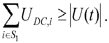
- Pulsing of the selected converter cell has no effect as long as sum of the DC-link voltages of the N-1 other converter cells 36 is larger than a momentary value of the line voltage, i.e. as long as ⁇ i ⁇ S 1 U DC , i ⁇ U t .
- pulsing of the selected converter cell 36 is started when, and preferably maintained as long as ⁇ i ⁇ S 1 U DC , i ⁇ U t ; and/or stopped when, and preferably suppressed as long as ⁇ i ⁇ S 1 U DC , i ⁇ U t .
- said cell is put into diode mode.
- Fig. 3 illustrates the various aspects of controlling the selected converter cell 36 as described above.
- Curve 71 shows the line voltages U(t) over one period.
- Horizontal lines 71a and 71 b indicate ⁇ i ⁇ S 1 U DC , i and - ⁇ i ⁇ S 1 U DC , i , respectively.
- Curve 72 illustrates an enable signal, which may be used to enable and disable pulsing of the power semiconductor switches 46a-d in order to put the selected converter cell 36 into active mode and diode mode, respectively.
- the methods may be simple to implement as an addition to an existing control method.
- the methods may provide a continuous adaptation of the switching strategy for different power levels while the overall control objectives are maintained. There is no additional hardware needed. All methods can work independently or in any combination, which enables the possibility to adapt the switching strategy based on the requirements for different applications.
- a ⁇ b implies that
- a statement a » b implies that a > 10 b , preferably a > 100 b ; and statement a ⁇ b implies that 10a ⁇ b, preferably 100a ⁇ b.
Landscapes
- Engineering & Computer Science (AREA)
- Power Engineering (AREA)
- Life Sciences & Earth Sciences (AREA)
- Sustainable Development (AREA)
- Sustainable Energy (AREA)
- Transportation (AREA)
- Mechanical Engineering (AREA)
- Rectifiers (AREA)
- Dc-Dc Converters (AREA)
Abstract
said modular converter in particular comprising a plurality of M converter cells (36), each converter cell comprising
an AC-to-DC converter (40), a primary side of which represents a primary side of said converter cell, said AC-to-DC converter being an active AC-to-DC converter comprising a plurality of semiconductor switches (46a-d), and operable in one of a plurality of modes, the plurality of modes comprising a bypassed mode, an active mode, and a diode mode; a DC-to-DC converter (42), a secondary side of which represents a secondary side of said converter cell; with
a secondary side of said AC-to-DC converter and a primary side of said DC-to-DC converter connected in parallel with a DC-link capacitor (50), wherein the primary sides of the converter cells are connected in series, with a first converter cell connected to a line (16), preferably a medium voltage line, providing an AC line voltage U(t) having a peak value Û, and an M-th converter cell connected to a ground (22);
the method comprising the steps of:
for a given allowable range [U min, U max] of a DC-voltage U DC at the DC-link capacitor determining whether any integer number N ≤ M exists for which
if such integer number N exists:
selecting an integer number L with L < N,
selecting a first set of N-L converter cells,
selecting a second set of L converter cells,
putting the AC-to-DC converter of, preferably all, converter cells which have not been selected in steps ii) or iii) into bypassed mode,
putting the AC-to-DC converter of, preferably all, converter cells from the first set into diode mode,
putting the AC-to-DC converter of, preferably all, converter cells from the second set into active mode.
Description
- The invention relates to a method for controlling a modular converter in accordance with the preamble of the independent patent claim.
- For an electric power supply of electric trains or trams, modular converters comprising a plurality of converter cells configured to produce from an AC input voltage a DC output voltage which may be supplied to electrical installations on-board have recently received growing attention. Usually, the AC input voltage is supplied from a line, in particular an overhead line.
- In an exemplary modular converter, each converter cell comprises a resonant DC-to-DC converter, which is connected to the line via an AC-to-DC converter. In the resonant DC-to-DC converter, a DC-to-AC converter on a line side is connected via a resonant transformer with a further AC-to-DC converter on a motor side. Both the DC-to-AC converter and the further AC-to-DC converter may be active converters comprising controllable semiconductor switches.
- Frequently, a control method for the modular converter is based on hard-switching of the AC-to-DC converters' semiconductor switches and soft-switching of the DC-to-DC converters' semiconductor switches, with low current switching during a turn-off, possibly in combination with zero voltage switching (ZVS) during a turn-on of the DC-to-DC converter semiconductors.
- As switching losses depend on voltage and current during switching, said switching method may result in low switching losses and thus in a high-efficiency AC-to-DC conversion at nominal power ratings.
- However, when this switching method is used under light-load or no-load conditions, the switching losses of the AC-to-DC converter cells stay approximately the same, but less power is transferred, and thus efficiency decreases. In an extreme case, when no power is required to be transferred by the converter cells, switching losses in almost equal amounts would nevertheless occur.
-
WO 2014/037406 A1 , which is hereby included by reference in its entirety, is concerned with enhancing the efficiency of a modular converter under low load or very low load conditions. Amongst other measures, this is achieved by operating the AC-to-DC converters in an intermittent mode. In said intermittent mode, in dependence on voltage and power capabilities, a first number of converter cells may be short circuited. For a second number of remaining converter cells, all AC-to-DC converters are put into an active mode when a DC-link voltage for one of the converter cells falls below an individual threshold; and are deactivated (or turned off) when a sum of all DC-link voltages of the remaining converter cells reaches a further threshold. - However, if a difference between individual thresholds and further threshold is selected sufficiently large, the DC-link voltages will oscillate between the individual threshold for the respective cell and the further threshold, which may lead to voltage oscillations and thus converter instabilities. On the other hand, if the difference between individual thresholds and further threshold is chosen relatively small, converter efficiency under low load and in particular under very low load operation remains unsatisfactory, due to the fact that the AC-to-DC converters remain in active mode.
- It is an object of the invention to provide a method for controlling of a modular converter which overcomes the disadvantages as discussed above.
- This object is achieved by a method in accordance with the independent patent claim.
- This object is achieved by the subject-matter of the independent patent claim. Further exemplary embodiments are evident from the dependent claims and the following description.
- A method in accordance with the invention for controlling a modular converter,
said modular converter in particular comprising a plurality of M converter cells, each converter cell comprising
an AC-to-DC converter, a primary side of which represents a primary side of said converter cell, said AC-to-DC converter being an active AC-to-DC converter comprising a plurality of semiconductor switches (46a-d), and operable in one of a plurality of modes, the plurality of modes comprising a bypassed mode, an active mode, and a diode mode;
a DC-to-DC converter, a secondary side of which represents a secondary side of said converter cell; with
a secondary side of said AC-to-DC converter and a primary side of said DC-to-DC converter connected in parallel with a DC-link capacitor, wherein
the primary sides of the converter cells are connected in series, with a first converter cell connected to a line, preferably a medium voltage line, providing an AC line voltage U(t) having a peak value Û, and an M-th converter cell connected to a ground;
comprises the steps of: - for a given allowable range [U min, U max] of a DC-voltage U DC at the DC-link capacitor determining whether any integer number N ≤ M exists for which

and
and - if such integer number N exists:
- selecting an integer number L with L < N,
- selecting a first set of N-L converter cells,
- selecting a second set of L converter cells,
- putting the AC-to-DC converter of, preferably all, converter cells which have not been selected in steps ii) or iii) into bypassed mode,
- putting the AC-to-DC converter of, preferably all, converter cells from the first set into diode mode,
- putting the AC-to-DC converter of, preferably all, converter cells from the second set into active mode.
- Summarized, the method provides an energy-efficient switching strategy for low and very low power ratings, not only at a nominal operating point. In particular, in traction applications power ratings change constantly during a load cycle, thus an availability of high efficiency over a whole range of power ratings is beneficial.
- Furthermore, the method provides a stable operation of the modular converter and may achieve the control objectives (sinusoidal input current and control of DC output voltage) under steady-state conditions for low and very low load conditions.
- A further aspect of the invention relates to a controller of a modular converter, wherein the controller is adapted for performing the method as described in the above and in the following. The controller may comprise a control unit providing switching signals to said AC-to-DC converter and said DC-to-DC converter, implementing one or more variants of the low load control method as described in the above and in the following.
- A further aspect of the invention relates to a modular converter for supplying a DC output voltage to at least one electrical motor, in general via a separate motor converter, in particular a motor inverter. For example, the electrical motor may be the motor of a train or a tram. It has to be understood that features of the method as described in the above and in the following may be features of the modular converter and the controller as described in the above and in the following, and vice versa.
- The modular converter may comprise a controller as described in the above and in the following. The controller or control unit may generate and provide switching signals to the AC-to-DC converter and to the DC-to-DC converter, in particular for pulsing of semiconductor switches comprised by said converters.
- The AC-to-DC converter may be a full-bridge converter, which is adapted for converting a first side AC voltage into a first side DC voltage, or vice versa.
- According to an embodiment of the invention, each DC-to-DC converter comprises a DC-to-AC sub-converter and an AC-to-DC sub-converter which are coupled via a transformer.
- The DC-to-DC converter may be a resonant converter, which is adapted for converting the first DC voltage to a second DC voltage, or vice versa.
- These and other aspects of the invention will become apparent from and elucidated with reference to the embodiments described hereinafter.
- The subject matter of the invention will be explained in more detail in the following text with reference to exemplary embodiments which are illustrated in the attached drawings.
-
Fig. 1 schematically shows a modular converter for use with a method according to an embodiment of the invention. -
Fig. 2 illustrates a dependence of DC-link voltages on line voltage and a number of active front-ends operated in a diode mode. -
Fig. 3 illustrates various aspects of controlling a selected converter cell in a method in accordance with the present invention. - In principle, identical parts are provided with the same reference symbols in the figures.
-
Fig. 1 shows an exemplarymodular converter 10 for an electric train or tram, which may also be referred to as power electronic transformer (PET) or power electronic traction transformer (PETT). In general, the modular converter may be adapted for transforming a medium AC voltage to a low or medium DC voltage. The converter has aninput 12 which is connectable to a catenary oroverhead line 16 for supplying theconverter 10 with a line voltage U(t), said line voltage U(t) having an AC frequency f line, a peak value Û and/or a root-mean-square value U g with, in general, U g = Û/√2, in particular a medium-voltage AC input voltage, through a pantograph 14 and an inductor. Exemplary nominal values for the AC frequency f line may be between 10 and 100Hz, in particular 162/3Hz, 25Hz, 50Hz or 60Hz. Theconverter 10 comprises anearthing point 18 for connecting theconverter 10 to anearth 22, e.g. throughwheels 20 of the train or tram. - The
converter 10 has a DC output comprising apositive DC output 24 and anegative DC output 25 for supplying a load of the train or tram with a DC output voltage of e.g. about 1 kV. The load may comprise an electric motor, generally connected to the DC output via a motor converter; electrical on-board installations; further converters and/or an auxiliary power supply. - The
converter 10 has a modular structure and comprises a plurality ofM converter cells 36, with eachconverter cell 36 being represented by a unique integer cell index i with i ∈ {1; ...; M}. Theconverter cells 36 each comprise two input terminals and two output terminals; and thus are four-terminal converter cells connected in series on a primary side 32, i.e. connected in series between theinput 12 and theearthing point 18 and in parallel on a secondary side 34, i.e. connected in parallel to the twooutputs - Only the first and the
second converter cell 36 are shown in detail. - Each
converter cell 36 comprises a short-circuit switch 38, an AC-to-DC converter 40 and a DC-to-DC converter 42. - The short-
circuit switch 38 of eachconverter cell 36 is connected in series to the short-circuit switches 38 of theother converter cells 36 and comprises two power semiconductor switches 44, in particular thyristors, connected in parallel in opposite directions. In general, the short-circuit switch 38 may comprise alternative kinds of switches, for example one or more electromechanical switches. By means of the short-circuit switch 38, the two input terminals of theconverter cell 36 may be short circuited, thus putting the AC-to-DC converter 40 of theconverter cell 36, and thus thewhole converter cell 36, into a bypassed mode. - The AC-to-
DC converter 40 is an active front end (AFE) with fourpower semiconductor switches DC converter 40 and the DC-to-DC converter 42 are connected via a primary side DC link, which comprises a primary sideDC link capacitor 50, which in turn comprises a first sub-capacitor 50a and a second sub-capacitor 50b connected in series. For reasons of brevity, primary side DC link and primary sideDC link capacitor 50 are simply referred to as DC link and DC link capacitor above and in what follows. An output of the DC-to-DC converter 42 of eachconverter cell 36 is connected in parallel with the outputs of the DC-to-DC converters 42 of theother converter cells 36. Input terminals of the AC-to-DC converter 40 are represented by, connectable to, or fixedly connected with input terminals of theconverter cell 36. A primary side of the AC-to-DC converter 40 thus represents a primary side of theconverter cell 36. - The DC-to-
DC converter 42 is a resonant converter and comprises a first sideresonant sub-converter 52, and a second sideresonant sub-converter 56, which are coupled via a resonant tank ortransformer 54. - The first side
resonant converter 52 is connected to theDC link capacitor 50 and comprises an upper and a lower pair of power semiconductor switches 58 connected in series. A first input of the primary side of thetransformer 54 is connected between the two pairs of power semiconductor switches 58. A second input of the primary side of thetransformer 54 is connected via a capacitor 60 to a point between the first sub-capacitor 50a and the second first sub-capacitor 50b of the DC-link capacitor 50. - Likewise, the second side
resonant converter 56 comprises an upper and a lower pair of power semiconductor switches 62 connected in series, which are connected in parallel with a secondary side DC link with third sub-capacitor 64a and a fourth sub-capacitor 64b connected in series to form a secondary side DC-link capacitor 64. One input of the secondary side of thetransformer 54 is connected between the two pairs of power semiconductor switches 62. The other input of the secondary side of thetransformer 54 is connected between the capacitors. - Exemplary, all the power semiconductor switches 44, 46a-d, 58, 62 are IGBTs.
- Each
converter cell 36 may comprise a local controller (not shown inFig. 1 ), which is adapted to control the semiconductor switches 44, 46a-d, 58, 62 of therespective converter cell 36. The local controllers may be communicatively interconnected with a main controller, which is adapted to control the local controllers. However, it is also possible that the main controller controls the semiconductor switches 44, 46a-d, 58, 62 directly. In particular, each of the semiconductor switches may independently be switched between a conducting and a blocking state, in particular a forward blocking state, by means of switching pulses applied by the controller. - When the modular converter is in operation under nominal conditions, the AC-to-
DC converters 40 are in an active mode, i.e. the four power semiconductor switches 46a-d of each of the AC-to-DC converters 40 are repeatedly switched by the controllers in a switching pattern appropriate to ensure a sufficient flow of electric power from the line into the DC-link capacitor 50. In particular, each of the four power semiconductor switches 46a-d is repeatedly switched between conducting and blocking state in an individual switching pattern. In general, switching is done at time scales substantially smaller than a period of the AC grid voltage. Both AC-to-DC converters 40 as well aspower semiconductor switches DC converters 40 are in active mode. Exemplary, the modular converter may be operated in a pulse width modulation (PWM) mode, so that for a sum over voltages U DC,i at each of the DC-link capacitors 50 with i ∈ {1; ...; M},
link capacitors 50, an allowed band of values [UDC,min, UDC,max] and a desired value UDC,opt ∈ [UDC,min, UDC,max] is defined. In general, pulsing is done with an average duration T pulsing between successive, identical switching operations, in particular periodically with a frequency f PWM, in particular a pulse width modulation frequency, resulting in T pulsing = 1/f PWM. Typically, f PWM >> f line, with typical values being 1000Hz < f line < 2000Hz. Under successive, identical switching operations, two successive switching operations in the same direction are to be understood, i.e. either two successive operations switching from blocking state to conducting state, or two successive operations switching from conducting state to blocking state. - Under a low load condition, in particular when a power P consumed at the DC output is significantly smaller than a nominal or rated power P nominal of the modular converter, in particular when 10 P < P nominal, it may be considered to operate the AC-to-
DC converters 40 in a diode mode, in which the four power semiconductor switches 46a-d are not pulsed. In particular, an AC-to-DC converter 40 may be regarded as being in diode mode during time intervals T diode when its four power semiconductor switches 46a-d are in a blocking state, where T diode > 2T pulsing, preferably T diode >> T pulsing and/or T diode ≈ 1/(2 f line) or T diode > 1/(2 f line) holds. However, depending on a load attached to the DC output, this would lead to a decrease of the voltages U DC,i at the DC-link capacitors 50, and subsequently a decrease in voltages U DC,out,i at the secondary side DC-link capacitors 64, and thus a voltage U DC,out at anoutput DC link 66 and at the DC output. - Under such circumstances, loads connected to DC output may no longer operate normally.
- To increase the voltages U DC,i at the DC-
link capacitors 50 while allowing for AC-to-DC converters 40 ofconverter cells 36 to be operated in diode mode, one or more electedconverter cells 36 may be bypassed, e.g. by means of the short-circuit switch 38 of the respective converter cell orcells 36, or by switching a zero vector with the AC-to-DC converter 40 of the respective converter cell orcells 36, leaving a first subset S1 c {1; ...; M} of |S1| converter cells in diode mode. As a consequence, the line voltage will effectively be divided by a smaller number ofconverter cells 36, resulting in a higher voltage U DC,j at the remaining converter cells with j ∈ S1 ⊂ {1; ...; M}. - However, for certain given bands of values [UDC,min, UDC,max] this approach only works for line voltages U(t) having peak value Û and/or root-mean-square values U g within certain ranges. This is illustrated in
Fig. 2 , which shows the voltages U DC,i at the DC-link capacitors 50 for different numbers |S1| ∈ {5; 6; 7; 8} ofconverter cells 36 in diode mode, where it was assumed that the DC-link capacitors of all converter cells are equal, and thus U DC, k = U DC,l = U DC for all k,l ∈ S1; and that a negligible amount of power P, preferably with 100 P < P nominal is drawn by the load at the DC output.Curve 70a shows the voltage U DC,i at the DC-link capacitors 50 for |S1| = 5,curve 70b for |S1| = 6,curve 70c for |S1| = 7, andcurve 70d for |S1| = 8. The horizontal lines at UDC,min = 3400V and UDC,max = 3800V illustrate an exemplary given bands of values [UDC,min, UDC,max]. As may be seen, for exemplary root-mean-square values U g/kV ∈ [13,4; 14,4], U g/kV ∈ [16,8; 18,8] of the line voltage, no number of converter cells in diode mode may be found for which U DC will be within the given band of values [3,4kV, 3,8kV]. In other words, for a given band of values [UDC,min, UDC,max], and certain peak values Û of the line voltage, a number N ≤ M exists for which Û/N < U min, but Û/(N-1) > U max. - In a preferred variant of the method in accordance with the invention, in a situation as described above, the AC-to-
DC converter 40 of one selectedconverter cell 36, represented by integer cell index s with s ∈ {1; ...; M}, is put into active mode, whereas the AC-to-DC converters 40 of N-1other converter cells 36 are operated in diode mode. Said N-1other converter cells 36 thus again represent a first subset S1 c {1; ...; M}, in particular S1 c {1; ...; M}\{s}, ofconverter cells 36 with |S1| = N-1; whereas the selectedconverter cell 36 represents a second subset {s} = S2 ⊂ {1; ...; M} ofconverter cells 36 with |S2| = 1 and S1 ∩ S2 = Ø. The remainingconverter cells 36, i.e. a third subset S3 = ({1; ...; M}\Si)\S2 ofconverter cells 36, are bypassed, e.g. by putting their respective AC-to-DC converters 40 into bypassed mode. The selectedconverter cell 36 acts as a boost cell. Due to the pulsing of the selectedconverter cell 36, higher values of a current l(t) flowing into themodular converter 10 can be achieved, which in turn will lead to an increase in DC-link voltages. - Preferably, in order to keep the DC-link voltages U DC,i of the selected
converter cell 36 and the N-1other converter cells 36 optimally balanced, i.e. to match U DC,k = U DC,l = U DC,opt as closely as possible for all k,l ∈ S1 ∪ S2, pulsing is done cyclically with all cells from S1 u S2, i.e. allconverter cells 36 in operation. In other words, the selectedconverter cell 36 is repeatedly, preferably periodically, exchanged against one of the N-1other converter cells 36; preferably against one of the N-1other converter cells 36 that has been in diode mode for a longest time out of all the N-1other converter cells 36. - Pulsing of the selected converter cell has no effect as long as sum of the DC-link voltages of the N-1
other converter cells 36 is larger than a momentary value of the line voltage, i.e. as long as
converter cell 36 is started when, and preferably maintained as long as
converter cell 36 is not pulsed, said cell is put into diode mode. Preferably, during periods when the selectedconverter cell 36 is being pulsed, the DC-link voltage U DC,s of the selectedconverter cell 36 is controlled by means of closed loop control based on a set value U DC,set ∈ [UDC,min, UDC,max], wherein the selectedconverter cell 36 is preferably operated in PWM mode, preferably with U DC,set = U DC,opt. -
Fig. 3 illustrates the various aspects of controlling the selectedconverter cell 36 as described above.Curve 71 shows the line voltages U(t) over one period.Horizontal lines 

Curve 72 illustrates an enable signal, which may be used to enable and disable pulsing of the power semiconductor switches 46a-d in order to put the selectedconverter cell 36 into active mode and diode mode, respectively. - With the above described methods, lower switching losses at light-load or no-load condition may be achieved and thus a high efficiency may be maintained over the whole power range, and/or over the whole load cycle.
- By applying this light-load strategy, it is possible to keep the efficiency of the
resonant converter 10 high under light-load and no-load conditions. The methods may be simple to implement as an addition to an existing control method. The methods may provide a continuous adaptation of the switching strategy for different power levels while the overall control objectives are maintained. There is no additional hardware needed. All methods can work independently or in any combination, which enables the possibility to adapt the switching strategy based on the requirements for different applications. - Unless stated otherwise, it is assumed that throughout this patent application, a statement a ≈ b implies that |a-b|/(|a|+|b|) < 10-1, preferably |a-b|/(|a|+|b|) < 10-2, wherein a and b may represent any mathematical, electric and/or physical quantities or other arbitrary variables as described and/or defined anywhere in this patent application, or as otherwise known to a person skilled in the art. Further, a statement that a is at least approximately equal or at least approximately identical to b implies that a ≈ b, preferably a = b. Further, unless stated otherwise, it is assumed that throughout this patent application, a statement a » b implies that a > 10b, preferably a > 100b; and statement a << b implies that 10a < b, preferably 100a < b.
- While the invention has been illustrated and described in detail in the drawings and foregoing description, such illustration and description are to be considered illustrative or exemplary and not restrictive; the invention is not limited to the disclosed embodiments. Other variations to the disclosed embodiments can be understood and effected by those skilled in the art and practising the claimed invention, from a study of the drawings, the disclosure, and the appended claims. In the claims, the word "comprising" does not exclude other elements or steps, and the indefinite article "a" or "an" does not exclude a plurality. A single processor or controller or other unit may fulfil the functions of several items recited in the claims. The mere fact that certain measures are recited in mutually different dependent claims does not indicate that a combination of these measures cannot be used to advantage. Any reference signs in the claims should not be construed as limiting the scope.
Claims (16)
- A method for controlling a modular converter (10),a) the modular converter (10) comprising a plurality of M converter cells (36), each converter cell comprisingi) an AC-to-DC converter (40), a primary side of which represents a primary side of said converter cell, said AC-to-DC converter being an active AC-to-DC converter comprising a plurality of semiconductor switches (46a-d), and operable in one of a plurality of modes, the plurality of modes comprising a bypassed mode, an active mode, and a diode mode;ii) a DC-to-DC converter (42), a secondary side of which represents a secondary side of said converter cell; withiii) a secondary side of said AC-to-DC converter and a primary side of said DC-to-DC converter connected in parallel with a DC-link capacitor (50), whereinb) the primary sides of the converter cells are connected in series, with a first converter cell connected to a line (16), preferably a medium voltage line, providing an AC line voltage U(t) having a peak value Û, and an M-th converter cell connected to a ground (22);the method comprising the steps of:c) for a given allowable range [U min, U max] of a DC-voltage U DC at the DC-link capacitori) determining whether any integer number N ≤ M exists for whichii) Û/N < U min, andiii) Û/(N-1) > U max; andd) if the condition under c) is fulfilledi) selecting an integer number L with L < N,ii) selecting a first set of N-L converter cells,iii) selecting a second set of L converter cells,iv) putting the AC-to-DC converter of, preferably all, converter cells which have not been selected in steps ii) or iii) into bypassed mode,v) putting the AC-to-DC converter of, preferably all, converter cells from the first set into diode mode,vi) putting the AC-to-DC converter of, preferably all, converter cells from the second set into active mode.
- The method according to claim 1, further characterized in that the secondary sides of the converter cells (36) are connected in parallel.
- The method according to claim 1 or 2, further characterized in that the converter cells selected in step d)ii) of claim 1 form a first subset S1 of the plurality of M converter cells (36); the converter cells selected in step d)iii) of claim 1 form a second subset S2 of the plurality of M converter cells (36); wherein S1 ∩ S2 = 0.
- The method according to one of the previous claims, further comprising the steps of selecting L = 1 in step d)i) of claim 1.
- The method according to one of the previous claims, further comprising the steps of:a) as long as the condition under c) of claim 1 is fulfilled,b) repeatedly:i) selecting a first converter cell from the first set of converter cells,ii) selecting a second converter cell from the second set of converter cells, andiii) assigning the first converter cell to the second set of converter cells, andiv) assigning the second converter cell to the first set of converter cells.
- The method of claim 5, wherein for a frequency f line of the line voltage, a maximum time span T between successive executions of steps b)i) to b)iv) of claim 5 is smaller than or at least approximately equal to 1/(2 f line).
- The method according to one of the previous claims, further comprising the steps of:a) for each converter cell (36) in the first set of converter cells,b) determining a DC-link voltage U DC,i at the DC-link capacitance of said converter cell (36),c) determining a sum U DC,∑ of DC-link voltages U DC ,j as U DC,∑ = ∑j=1 N-L UDC,j,d) putting converter cells, preferably all converter cells, from the second set into active mode when |U(t)| > U DC,∑ .
- The method according to one of the previous claims, further comprising the steps of:a) for each converter cell (36) in the first set of converter cellsb) determining a DC-link voltage U DC,i at the DC-link capacitancec) determining a sum U DC,∑ of DC-link voltages U DC,j as U DC,∑ = ∑ j=1 N-L U DC, j,d) putting converter cells, preferably all converter cells, from the second set into diode mode when |U(t)| < U DC,∑.
- The method according to one of the previous claims, further comprising the step of operating the active cells in a PWM mode, wherein semiconductor switches of said converter cell are switched with a PWM frequency f PWM, preferably with f line << f PWM.
- The method according to the previous claim, further comprising the step of controlling PWM pulses for switching the semiconductor switches of active cells by means of closed loop control based on a set value U DC set for the DC-link voltages of the active cells with U DC,set E [U min, U max].
- The method according to one of the previous claims, further characterized by bypassing converter cells (36) which have not been selected in step ii) or iii) of claim 1 by short circuiting a primary side of said converter cells.
- The method according to one of the previous claims, further characterized in that when an AC-to-DC converter of a converter cell is in active mode, its semiconductor switches (46a-d) are repeatedly switched with an average duration T pulsing between successive, identical switching operations, preferably with T pulsing << 1/f line, where f line is an AC frequency of the AC line voltage U(t).
- The method according to claim 12, further characterized in that in order to put an AC-to-DC converter of a converter cell into diode mode its semiconductor switches (46a-d) are set to blocking state, preferably for a time interval T diode where T diode > 2T pulsing, preferably T diode >> T pulsing.
- A controller for controlling a modular converter (10),a) the modular converter (10) comprising a plurality of M converter cells (36), each converter cell comprisingi) an AC-to-DC converter, a primary side of which represents a primary side of said converter cell, said AC-to-DC converter being an active AC-to-DC converter comprising a plurality of semiconductor switches, and operable in one of a plurality of modes, the plurality of modes comprising a bypassed mode, an active mode, and a diode mode,ii) a DC-to-DC converter, a secondary side of which represents a secondary side of said converter cell, withiii) a secondary side of said AC-to-DC converter and a primary side of said DC-to-DC converter connected in parallel with a DC-link capacitance; whereinb) the primary sides of the converter cells are connected in series, with a first converter cell connected to a line, preferably a medium voltage line, providing an AC line voltage U(t) having a peak value Û, and an M-th converter cell connected to a ground;
the controller configured to perform the method according to one of claims 1 through 13. - The controller according to claim 14, further characterized in that the controller is configured to repeatedly switch the semiconductor switches (46a-d) of an AC-to-DC converter of a converter cell in order to put said AC-to-DC converter into active mode, with an average duration T pulsing between successive, identical switching operations, preferably with T pulsing << 1/f line, where f line is an AC frequency of the AC line voltage U(t).
- The controller according to claim 15, further characterized in that the controller is configured to set the semiconductor switches (46a-d) of an AC-to-DC converter of a converter cell to a blocking state, preferably for a time interval T diode where T diode > 2T pulsing, preferably T diode >> T pulsing, in order to put said AC-to-DC converter into diode mode.
Priority Applications (1)
| Application Number | Priority Date | Filing Date | Title |
|---|---|---|---|
| EP15182880.3A EP2995495B1 (en) | 2014-09-15 | 2015-08-28 | Method for controlling of a modular converter |
Applications Claiming Priority (2)
| Application Number | Priority Date | Filing Date | Title |
|---|---|---|---|
| EP14184794 | 2014-09-15 | ||
| EP15182880.3A EP2995495B1 (en) | 2014-09-15 | 2015-08-28 | Method for controlling of a modular converter |
Publications (2)
| Publication Number | Publication Date |
|---|---|
| EP2995495A1 true EP2995495A1 (en) | 2016-03-16 |
| EP2995495B1 EP2995495B1 (en) | 2019-06-19 |
Family
ID=51535381
Family Applications (1)
| Application Number | Title | Priority Date | Filing Date |
|---|---|---|---|
| EP15182880.3A Active EP2995495B1 (en) | 2014-09-15 | 2015-08-28 | Method for controlling of a modular converter |
Country Status (3)
| Country | Link |
|---|---|
| US (1) | US9571000B2 (en) |
| EP (1) | EP2995495B1 (en) |
| CN (1) | CN105429489B (en) |
Cited By (2)
| Publication number | Priority date | Publication date | Assignee | Title |
|---|---|---|---|---|
| CN111146951A (en) * | 2020-01-20 | 2020-05-12 | 特变电工西安电气科技有限公司 | Power electronic transformer capable of being started in two directions and control strategy thereof |
| EP3813243A1 (en) * | 2019-10-25 | 2021-04-28 | Kabushiki Kaisha Toshiba | Power switcher, power rectifier, and power converter |
Families Citing this family (11)
| Publication number | Priority date | Publication date | Assignee | Title |
|---|---|---|---|---|
| EP3023291A1 (en) * | 2014-11-20 | 2016-05-25 | ABB Technology AG | Converter system for electrical drive mechanism for a rail vehicle |
| US10027240B1 (en) | 2017-01-06 | 2018-07-17 | General Electric Company | Ground fault isolation for power converters with silicon carbide MOSFETs |
| US10110149B2 (en) | 2017-01-06 | 2018-10-23 | General Electric Company | Grounding scheme for power converters with silicon carbide MOSFETs |
| EP3410590A1 (en) * | 2017-06-02 | 2018-12-05 | General Electric Technology GmbH | Improvements in or relating to converters for interconnecting first and second electrical networks |
| WO2018229915A1 (en) * | 2017-06-14 | 2018-12-20 | 株式会社日立製作所 | Power conversion device and power conversion device connection method |
| CN107834866A (en) * | 2017-11-24 | 2018-03-23 | 中国矿业大学(北京) | Mining 127V AC powers |
| FI128052B (en) * | 2018-04-16 | 2019-08-30 | Lappeenrannan Teknillinen Yliopisto | Power converter for a bioelectrochemical system |
| CN110677060B (en) * | 2018-07-02 | 2021-08-03 | 台达电子工业股份有限公司 | Power conversion system and method for precharging DC bus capacitor therein |
| US11496053B2 (en) * | 2018-07-02 | 2022-11-08 | Delta Electronics, Inc. | Power conversion system with dc-bus pre-charge |
| CN110232234B (en) * | 2019-06-04 | 2021-06-04 | 华北电力大学 | A kind of PETT oscillation regulating device and IGBT sub-module manufacturing method |
| CN112994410B (en) * | 2019-12-16 | 2022-03-11 | 国创移动能源创新中心(江苏)有限公司 | Voltage equalization control device and method for DC bus capacitor of power electronic transformer system |
Citations (4)
| Publication number | Priority date | Publication date | Assignee | Title |
|---|---|---|---|---|
| DE102010039699A1 (en) * | 2010-08-24 | 2012-03-01 | Siemens Aktiengesellschaft | Drive system for a rail vehicle |
| DE102010044322A1 (en) * | 2010-09-03 | 2012-03-08 | Bombardier Transportation Gmbh | Electrical power supply arrangement for drive devices of rail vehicles |
| EP2703208A1 (en) * | 2012-09-04 | 2014-03-05 | ABB Technology AG | Controlling a modular converter |
| WO2014041192A1 (en) * | 2012-09-17 | 2014-03-20 | Abb Technology Ag | Energy management system for railbound vehicles |
Family Cites Families (4)
| Publication number | Priority date | Publication date | Assignee | Title |
|---|---|---|---|---|
| EP1750363A1 (en) * | 2005-08-03 | 2007-02-07 | Abb Research Ltd. | Multilevel AC/DC converter for traction applications |
| EP1750361A1 (en) * | 2005-08-03 | 2007-02-07 | ABB Research Ltd | Multilevel converter arrangement and use thereof |
| DE102009008549A1 (en) * | 2009-02-12 | 2010-08-19 | Bombardier Transportation Gmbh | Arrangement for operating loads in a rail vehicle with electrical energy, optionally from a power supply network or from a motor-generator combination |
| US8896280B2 (en) * | 2011-07-29 | 2014-11-25 | Infineon Technologies Austria Ag | Switching regulator with increased light load efficiency |
-
2015
- 2015-08-28 EP EP15182880.3A patent/EP2995495B1/en active Active
- 2015-09-11 US US14/851,161 patent/US9571000B2/en active Active
- 2015-09-15 CN CN201510587604.5A patent/CN105429489B/en active Active
Patent Citations (5)
| Publication number | Priority date | Publication date | Assignee | Title |
|---|---|---|---|---|
| DE102010039699A1 (en) * | 2010-08-24 | 2012-03-01 | Siemens Aktiengesellschaft | Drive system for a rail vehicle |
| DE102010044322A1 (en) * | 2010-09-03 | 2012-03-08 | Bombardier Transportation Gmbh | Electrical power supply arrangement for drive devices of rail vehicles |
| EP2703208A1 (en) * | 2012-09-04 | 2014-03-05 | ABB Technology AG | Controlling a modular converter |
| WO2014037406A1 (en) | 2012-09-04 | 2014-03-13 | Abb Technology Ag | Controlling a modular converter |
| WO2014041192A1 (en) * | 2012-09-17 | 2014-03-20 | Abb Technology Ag | Energy management system for railbound vehicles |
Non-Patent Citations (2)
| Title |
|---|
| MAX CLAESSENS ET AL: "1 Traction transformation 11 Traction transformation A power-electronic traction transformer (PETT)", ABB REVIEW, 10 April 2012 (2012-04-10), XP055151309, Retrieved from the Internet <URL:http://www05.abb.com/global/scot/scot271.nsf/veritydisplay/fc192d38056fa3b3c12579f20055483b/$file/11-17 1m211_en_72dpi.pdf> [retrieved on 20141106] * |
| MICHAEL STEINER ET AL: "Medium frequency topology in railway applications", 2007 EUROPEAN CONFERENCE ON POWER ELECTRONICS AND APPLICATIONS, 2007, pages 1 - 10, XP055048811, DOI: 10.1109/EPE.2007.4417570 * |
Cited By (4)
| Publication number | Priority date | Publication date | Assignee | Title |
|---|---|---|---|---|
| EP3813243A1 (en) * | 2019-10-25 | 2021-04-28 | Kabushiki Kaisha Toshiba | Power switcher, power rectifier, and power converter |
| JP2021069232A (en) * | 2019-10-25 | 2021-04-30 | 株式会社東芝 | Power switcher, power rectifier, and power converter |
| US11451161B2 (en) | 2019-10-25 | 2022-09-20 | Kabushiki Kaisha Toshiba | Power switcher, power rectifier, and power converter including cascode-connected transistors |
| CN111146951A (en) * | 2020-01-20 | 2020-05-12 | 特变电工西安电气科技有限公司 | Power electronic transformer capable of being started in two directions and control strategy thereof |
Also Published As
| Publication number | Publication date |
|---|---|
| US20160079879A1 (en) | 2016-03-17 |
| CN105429489B (en) | 2018-05-08 |
| CN105429489A (en) | 2016-03-23 |
| EP2995495B1 (en) | 2019-06-19 |
| US9571000B2 (en) | 2017-02-14 |
Similar Documents
| Publication | Publication Date | Title |
|---|---|---|
| EP2995495B1 (en) | Method for controlling of a modular converter | |
| EP2892752B1 (en) | Controlling a modular converter | |
| US9533632B2 (en) | Track-bound vehicle converter | |
| TW200608691A (en) | System and method for controlling a variable speed drive | |
| US7906922B2 (en) | Electric motor drive employing hybrid, hysteretic/pulse-width-modulated dynamic braking | |
| EP2833536A1 (en) | Inverter device | |
| WO2011000511A3 (en) | Control methods for parallel-connected power converters | |
| US20140132203A1 (en) | Apparatus and method for charging an electrical energy store from an ac voltage source | |
| US20150016162A1 (en) | Photovoltaic inverter with swinging line filter inductors | |
| KR102665350B1 (en) | Dual-Active-Bridge CONVERTER and BIPOLAR DC POWER DISTRIBUTION DEVICE | |
| JP6140007B2 (en) | Power converter | |
| JP5881362B2 (en) | Power converter | |
| Li et al. | Optimal synergetic control of a three-phase two-stage ultra-wide output voltage range EV battery charger employing a novel hybrid quantum series resonant DC/DC converter | |
| CN102820797A (en) | Inverter device adopting multi-winding transformer and multi-H-bridge structure and voltage output method thereof | |
| EP2704302B1 (en) | Switching a DC-to-DC converter | |
| US7859867B2 (en) | Method and inverter for converting a DC voltage into a 3-phase AC output | |
| KR20240095238A (en) | Power converter control method using variable switching frequency | |
| JP2019508008A (en) | Energy regenerative rectifier | |
| RU52539U1 (en) | MULTILEVEL AUTONOMOUS PHASE VOLTAGE INVERTER | |
| Kannan et al. | A Multilevel Inverter With a Single Battery Source and a High-Frequency Link for Electric Vehicles | |
| EP4496199A1 (en) | Converter for transferring power and corresponding method | |
| EP4496200A1 (en) | Converter for transferring power and corresponding method | |
| RU37489U1 (en) | THREE-PHASE VEHICLE ELECTRIC DRIVE | |
| RU144402U1 (en) | PULSE TRANSFORMER INVERTER |
Legal Events
| Date | Code | Title | Description |
|---|---|---|---|
| PUAI | Public reference made under article 153(3) epc to a published international application that has entered the european phase |
Free format text: ORIGINAL CODE: 0009012 |
|
| AK | Designated contracting states |
Kind code of ref document: A1 Designated state(s): AL AT BE BG CH CY CZ DE DK EE ES FI FR GB GR HR HU IE IS IT LI LT LU LV MC MK MT NL NO PL PT RO RS SE SI SK SM TR |
|
| AX | Request for extension of the european patent |
Extension state: BA ME |
|
| 17P | Request for examination filed |
Effective date: 20160916 |
|
| RBV | Designated contracting states (corrected) |
Designated state(s): AL AT BE BG CH CY CZ DE DK EE ES FI FR GB GR HR HU IE IS IT LI LT LU LV MC MK MT NL NO PL PT RO RS SE SI SK SM TR |
|
| RAP1 | Party data changed (applicant data changed or rights of an application transferred) |
Owner name: ABB SCHWEIZ AG |
|
| GRAP | Despatch of communication of intention to grant a patent |
Free format text: ORIGINAL CODE: EPIDOSNIGR1 |
|
| STAA | Information on the status of an ep patent application or granted ep patent |
Free format text: STATUS: GRANT OF PATENT IS INTENDED |
|
| INTG | Intention to grant announced |
Effective date: 20181129 |
|
| GRAS | Grant fee paid |
Free format text: ORIGINAL CODE: EPIDOSNIGR3 |
|
| GRAA | (expected) grant |
Free format text: ORIGINAL CODE: 0009210 |
|
| STAA | Information on the status of an ep patent application or granted ep patent |
Free format text: STATUS: THE PATENT HAS BEEN GRANTED |
|
| RIN1 | Information on inventor provided before grant (corrected) |
Inventor name: RONNER, BEAT |
|
| AK | Designated contracting states |
Kind code of ref document: B1 Designated state(s): AL AT BE BG CH CY CZ DE DK EE ES FI FR GB GR HR HU IE IS IT LI LT LU LV MC MK MT NL NO PL PT RO RS SE SI SK SM TR |
|
| REG | Reference to a national code |
Ref country code: GB Ref legal event code: FG4D |
|
| REG | Reference to a national code |
Ref country code: CH Ref legal event code: EP |
|
| REG | Reference to a national code |
Ref country code: IE Ref legal event code: FG4D |
|
| REG | Reference to a national code |
Ref country code: DE Ref legal event code: R096 Ref document number: 602015032134 Country of ref document: DE |
|
| REG | Reference to a national code |
Ref country code: AT Ref legal event code: REF Ref document number: 1145045 Country of ref document: AT Kind code of ref document: T Effective date: 20190715 |
|
| REG | Reference to a national code |
Ref country code: NL Ref legal event code: MP Effective date: 20190619 |
|
| PG25 | Lapsed in a contracting state [announced via postgrant information from national office to epo] |
Ref country code: LT Free format text: LAPSE BECAUSE OF FAILURE TO SUBMIT A TRANSLATION OF THE DESCRIPTION OR TO PAY THE FEE WITHIN THE PRESCRIBED TIME-LIMIT Effective date: 20190619 Ref country code: HR Free format text: LAPSE BECAUSE OF FAILURE TO SUBMIT A TRANSLATION OF THE DESCRIPTION OR TO PAY THE FEE WITHIN THE PRESCRIBED TIME-LIMIT Effective date: 20190619 Ref country code: FI Free format text: LAPSE BECAUSE OF FAILURE TO SUBMIT A TRANSLATION OF THE DESCRIPTION OR TO PAY THE FEE WITHIN THE PRESCRIBED TIME-LIMIT Effective date: 20190619 Ref country code: NO Free format text: LAPSE BECAUSE OF FAILURE TO SUBMIT A TRANSLATION OF THE DESCRIPTION OR TO PAY THE FEE WITHIN THE PRESCRIBED TIME-LIMIT Effective date: 20190919 Ref country code: AL Free format text: LAPSE BECAUSE OF FAILURE TO SUBMIT A TRANSLATION OF THE DESCRIPTION OR TO PAY THE FEE WITHIN THE PRESCRIBED TIME-LIMIT Effective date: 20190619 Ref country code: SE Free format text: LAPSE BECAUSE OF FAILURE TO SUBMIT A TRANSLATION OF THE DESCRIPTION OR TO PAY THE FEE WITHIN THE PRESCRIBED TIME-LIMIT Effective date: 20190619 |
|
| REG | Reference to a national code |
Ref country code: LT Ref legal event code: MG4D |
|
| PG25 | Lapsed in a contracting state [announced via postgrant information from national office to epo] |
Ref country code: LV Free format text: LAPSE BECAUSE OF FAILURE TO SUBMIT A TRANSLATION OF THE DESCRIPTION OR TO PAY THE FEE WITHIN THE PRESCRIBED TIME-LIMIT Effective date: 20190619 Ref country code: GR Free format text: LAPSE BECAUSE OF FAILURE TO SUBMIT A TRANSLATION OF THE DESCRIPTION OR TO PAY THE FEE WITHIN THE PRESCRIBED TIME-LIMIT Effective date: 20190920 Ref country code: BG Free format text: LAPSE BECAUSE OF FAILURE TO SUBMIT A TRANSLATION OF THE DESCRIPTION OR TO PAY THE FEE WITHIN THE PRESCRIBED TIME-LIMIT Effective date: 20190919 Ref country code: RS Free format text: LAPSE BECAUSE OF FAILURE TO SUBMIT A TRANSLATION OF THE DESCRIPTION OR TO PAY THE FEE WITHIN THE PRESCRIBED TIME-LIMIT Effective date: 20190619 |
|
| REG | Reference to a national code |
Ref country code: AT Ref legal event code: MK05 Ref document number: 1145045 Country of ref document: AT Kind code of ref document: T Effective date: 20190619 |
|
| PG25 | Lapsed in a contracting state [announced via postgrant information from national office to epo] |
Ref country code: NL Free format text: LAPSE BECAUSE OF FAILURE TO SUBMIT A TRANSLATION OF THE DESCRIPTION OR TO PAY THE FEE WITHIN THE PRESCRIBED TIME-LIMIT Effective date: 20190619 Ref country code: CZ Free format text: LAPSE BECAUSE OF FAILURE TO SUBMIT A TRANSLATION OF THE DESCRIPTION OR TO PAY THE FEE WITHIN THE PRESCRIBED TIME-LIMIT Effective date: 20190619 Ref country code: RO Free format text: LAPSE BECAUSE OF FAILURE TO SUBMIT A TRANSLATION OF THE DESCRIPTION OR TO PAY THE FEE WITHIN THE PRESCRIBED TIME-LIMIT Effective date: 20190619 Ref country code: SK Free format text: LAPSE BECAUSE OF FAILURE TO SUBMIT A TRANSLATION OF THE DESCRIPTION OR TO PAY THE FEE WITHIN THE PRESCRIBED TIME-LIMIT Effective date: 20190619 Ref country code: EE Free format text: LAPSE BECAUSE OF FAILURE TO SUBMIT A TRANSLATION OF THE DESCRIPTION OR TO PAY THE FEE WITHIN THE PRESCRIBED TIME-LIMIT Effective date: 20190619 Ref country code: AT Free format text: LAPSE BECAUSE OF FAILURE TO SUBMIT A TRANSLATION OF THE DESCRIPTION OR TO PAY THE FEE WITHIN THE PRESCRIBED TIME-LIMIT Effective date: 20190619 Ref country code: PT Free format text: LAPSE BECAUSE OF FAILURE TO SUBMIT A TRANSLATION OF THE DESCRIPTION OR TO PAY THE FEE WITHIN THE PRESCRIBED TIME-LIMIT Effective date: 20191021 |
|
| PG25 | Lapsed in a contracting state [announced via postgrant information from national office to epo] |
Ref country code: ES Free format text: LAPSE BECAUSE OF FAILURE TO SUBMIT A TRANSLATION OF THE DESCRIPTION OR TO PAY THE FEE WITHIN THE PRESCRIBED TIME-LIMIT Effective date: 20190619 Ref country code: IT Free format text: LAPSE BECAUSE OF FAILURE TO SUBMIT A TRANSLATION OF THE DESCRIPTION OR TO PAY THE FEE WITHIN THE PRESCRIBED TIME-LIMIT Effective date: 20190619 Ref country code: SM Free format text: LAPSE BECAUSE OF FAILURE TO SUBMIT A TRANSLATION OF THE DESCRIPTION OR TO PAY THE FEE WITHIN THE PRESCRIBED TIME-LIMIT Effective date: 20190619 Ref country code: IS Free format text: LAPSE BECAUSE OF FAILURE TO SUBMIT A TRANSLATION OF THE DESCRIPTION OR TO PAY THE FEE WITHIN THE PRESCRIBED TIME-LIMIT Effective date: 20191019 |
|
| PG25 | Lapsed in a contracting state [announced via postgrant information from national office to epo] |
Ref country code: TR Free format text: LAPSE BECAUSE OF FAILURE TO SUBMIT A TRANSLATION OF THE DESCRIPTION OR TO PAY THE FEE WITHIN THE PRESCRIBED TIME-LIMIT Effective date: 20190619 |
|
| PG25 | Lapsed in a contracting state [announced via postgrant information from national office to epo] |
Ref country code: PL Free format text: LAPSE BECAUSE OF FAILURE TO SUBMIT A TRANSLATION OF THE DESCRIPTION OR TO PAY THE FEE WITHIN THE PRESCRIBED TIME-LIMIT Effective date: 20190619 Ref country code: DK Free format text: LAPSE BECAUSE OF FAILURE TO SUBMIT A TRANSLATION OF THE DESCRIPTION OR TO PAY THE FEE WITHIN THE PRESCRIBED TIME-LIMIT Effective date: 20190619 |
|
| PG25 | Lapsed in a contracting state [announced via postgrant information from national office to epo] |
Ref country code: LU Free format text: LAPSE BECAUSE OF NON-PAYMENT OF DUE FEES Effective date: 20190828 Ref country code: MC Free format text: LAPSE BECAUSE OF FAILURE TO SUBMIT A TRANSLATION OF THE DESCRIPTION OR TO PAY THE FEE WITHIN THE PRESCRIBED TIME-LIMIT Effective date: 20190619 Ref country code: IS Free format text: LAPSE BECAUSE OF FAILURE TO SUBMIT A TRANSLATION OF THE DESCRIPTION OR TO PAY THE FEE WITHIN THE PRESCRIBED TIME-LIMIT Effective date: 20200224 |
|
| REG | Reference to a national code |
Ref country code: BE Ref legal event code: MM Effective date: 20190831 |
|
| REG | Reference to a national code |
Ref country code: DE Ref legal event code: R097 Ref document number: 602015032134 Country of ref document: DE |
|
| PLBE | No opposition filed within time limit |
Free format text: ORIGINAL CODE: 0009261 |
|
| STAA | Information on the status of an ep patent application or granted ep patent |
Free format text: STATUS: NO OPPOSITION FILED WITHIN TIME LIMIT |
|
| PG2D | Information on lapse in contracting state deleted |
Ref country code: IS |
|
| PG25 | Lapsed in a contracting state [announced via postgrant information from national office to epo] |
Ref country code: IE Free format text: LAPSE BECAUSE OF NON-PAYMENT OF DUE FEES Effective date: 20190828 |
|
| 26N | No opposition filed |
Effective date: 20200603 |
|
| PG25 | Lapsed in a contracting state [announced via postgrant information from national office to epo] |
Ref country code: BE Free format text: LAPSE BECAUSE OF NON-PAYMENT OF DUE FEES Effective date: 20190831 Ref country code: SI Free format text: LAPSE BECAUSE OF FAILURE TO SUBMIT A TRANSLATION OF THE DESCRIPTION OR TO PAY THE FEE WITHIN THE PRESCRIBED TIME-LIMIT Effective date: 20190619 |
|
| PG25 | Lapsed in a contracting state [announced via postgrant information from national office to epo] |
Ref country code: CY Free format text: LAPSE BECAUSE OF FAILURE TO SUBMIT A TRANSLATION OF THE DESCRIPTION OR TO PAY THE FEE WITHIN THE PRESCRIBED TIME-LIMIT Effective date: 20190619 |
|
| PG25 | Lapsed in a contracting state [announced via postgrant information from national office to epo] |
Ref country code: HU Free format text: LAPSE BECAUSE OF FAILURE TO SUBMIT A TRANSLATION OF THE DESCRIPTION OR TO PAY THE FEE WITHIN THE PRESCRIBED TIME-LIMIT; INVALID AB INITIO Effective date: 20150828 Ref country code: MT Free format text: LAPSE BECAUSE OF FAILURE TO SUBMIT A TRANSLATION OF THE DESCRIPTION OR TO PAY THE FEE WITHIN THE PRESCRIBED TIME-LIMIT Effective date: 20190619 |
|
| PG25 | Lapsed in a contracting state [announced via postgrant information from national office to epo] |
Ref country code: MK Free format text: LAPSE BECAUSE OF FAILURE TO SUBMIT A TRANSLATION OF THE DESCRIPTION OR TO PAY THE FEE WITHIN THE PRESCRIBED TIME-LIMIT Effective date: 20190619 |
|
| PGFP | Annual fee paid to national office [announced via postgrant information from national office to epo] |
Ref country code: DE Payment date: 20250820 Year of fee payment: 11 |
|
| PGFP | Annual fee paid to national office [announced via postgrant information from national office to epo] |
Ref country code: GB Payment date: 20250821 Year of fee payment: 11 |
|
| PGFP | Annual fee paid to national office [announced via postgrant information from national office to epo] |
Ref country code: FR Payment date: 20250829 Year of fee payment: 11 |
|
| PGFP | Annual fee paid to national office [announced via postgrant information from national office to epo] |
Ref country code: CH Payment date: 20250901 Year of fee payment: 11 |