EP2996146B1 - Assemblage de boîtiers semi-conducteurs - Google Patents
Assemblage de boîtiers semi-conducteurs Download PDFInfo
- Publication number
- EP2996146B1 EP2996146B1 EP15177483.3A EP15177483A EP2996146B1 EP 2996146 B1 EP2996146 B1 EP 2996146B1 EP 15177483 A EP15177483 A EP 15177483A EP 2996146 B1 EP2996146 B1 EP 2996146B1
- Authority
- EP
- European Patent Office
- Prior art keywords
- die
- dram
- package
- soc
- semiconductor package
- Prior art date
- Legal status (The legal status is an assumption and is not a legal conclusion. Google has not performed a legal analysis and makes no representation as to the accuracy of the status listed.)
- Active
Links
Images

Classifications
-
- H—ELECTRICITY
- H10—SEMICONDUCTOR DEVICES; ELECTRIC SOLID-STATE DEVICES NOT OTHERWISE PROVIDED FOR
- H10W—GENERIC PACKAGES, INTERCONNECTIONS, CONNECTORS OR OTHER CONSTRUCTIONAL DETAILS OF DEVICES COVERED BY CLASS H10
- H10W90/00—Package configurations
-
- H—ELECTRICITY
- H05—ELECTRIC TECHNIQUES NOT OTHERWISE PROVIDED FOR
- H05K—PRINTED CIRCUITS; CASINGS OR CONSTRUCTIONAL DETAILS OF ELECTRIC APPARATUS; MANUFACTURE OF ASSEMBLAGES OF ELECTRICAL COMPONENTS
- H05K1/00—Printed circuits
- H05K1/02—Details
- H05K1/11—Printed elements for providing electric connections to or between printed circuits
- H05K1/111—Pads for surface mounting, e.g. lay-out
- H05K1/112—Pads for surface mounting, e.g. lay-out directly combined with via connections
-
- H—ELECTRICITY
- H05—ELECTRIC TECHNIQUES NOT OTHERWISE PROVIDED FOR
- H05K—PRINTED CIRCUITS; CASINGS OR CONSTRUCTIONAL DETAILS OF ELECTRIC APPARATUS; MANUFACTURE OF ASSEMBLAGES OF ELECTRICAL COMPONENTS
- H05K1/00—Printed circuits
- H05K1/18—Printed circuits structurally associated with non-printed electric components
- H05K1/181—Printed circuits structurally associated with non-printed electric components associated with surface mounted components
-
- H—ELECTRICITY
- H10—SEMICONDUCTOR DEVICES; ELECTRIC SOLID-STATE DEVICES NOT OTHERWISE PROVIDED FOR
- H10W—GENERIC PACKAGES, INTERCONNECTIONS, CONNECTORS OR OTHER CONSTRUCTIONAL DETAILS OF DEVICES COVERED BY CLASS H10
- H10W20/00—Interconnections in chips, wafers or substrates
- H10W20/20—Interconnections within wafers or substrates, e.g. through-silicon vias [TSV]
-
- H—ELECTRICITY
- H10—SEMICONDUCTOR DEVICES; ELECTRIC SOLID-STATE DEVICES NOT OTHERWISE PROVIDED FOR
- H10W—GENERIC PACKAGES, INTERCONNECTIONS, CONNECTORS OR OTHER CONSTRUCTIONAL DETAILS OF DEVICES COVERED BY CLASS H10
- H10W72/00—Interconnections or connectors in packages
-
- H—ELECTRICITY
- H10—SEMICONDUCTOR DEVICES; ELECTRIC SOLID-STATE DEVICES NOT OTHERWISE PROVIDED FOR
- H10W—GENERIC PACKAGES, INTERCONNECTIONS, CONNECTORS OR OTHER CONSTRUCTIONAL DETAILS OF DEVICES COVERED BY CLASS H10
- H10W72/00—Interconnections or connectors in packages
- H10W72/20—Bump connectors, e.g. solder bumps or copper pillars; Dummy bumps; Thermal bumps
-
- H—ELECTRICITY
- H10—SEMICONDUCTOR DEVICES; ELECTRIC SOLID-STATE DEVICES NOT OTHERWISE PROVIDED FOR
- H10W—GENERIC PACKAGES, INTERCONNECTIONS, CONNECTORS OR OTHER CONSTRUCTIONAL DETAILS OF DEVICES COVERED BY CLASS H10
- H10W72/00—Interconnections or connectors in packages
- H10W72/50—Bond wires
-
- H—ELECTRICITY
- H10—SEMICONDUCTOR DEVICES; ELECTRIC SOLID-STATE DEVICES NOT OTHERWISE PROVIDED FOR
- H10W—GENERIC PACKAGES, INTERCONNECTIONS, CONNECTORS OR OTHER CONSTRUCTIONAL DETAILS OF DEVICES COVERED BY CLASS H10
- H10W74/00—Encapsulations, e.g. protective coatings
- H10W74/10—Encapsulations, e.g. protective coatings characterised by their shape or disposition
- H10W74/111—Encapsulations, e.g. protective coatings characterised by their shape or disposition the semiconductor body being completely enclosed
- H10W74/129—Encapsulations, e.g. protective coatings characterised by their shape or disposition the semiconductor body being completely enclosed forming a chip-scale package [CSP]
-
- H—ELECTRICITY
- H10—SEMICONDUCTOR DEVICES; ELECTRIC SOLID-STATE DEVICES NOT OTHERWISE PROVIDED FOR
- H10W—GENERIC PACKAGES, INTERCONNECTIONS, CONNECTORS OR OTHER CONSTRUCTIONAL DETAILS OF DEVICES COVERED BY CLASS H10
- H10W70/00—Package substrates; Interposers; Redistribution layers [RDL]
- H10W70/60—Insulating or insulated package substrates; Interposers; Redistribution layers
-
- H—ELECTRICITY
- H10—SEMICONDUCTOR DEVICES; ELECTRIC SOLID-STATE DEVICES NOT OTHERWISE PROVIDED FOR
- H10W—GENERIC PACKAGES, INTERCONNECTIONS, CONNECTORS OR OTHER CONSTRUCTIONAL DETAILS OF DEVICES COVERED BY CLASS H10
- H10W70/00—Package substrates; Interposers; Redistribution layers [RDL]
- H10W70/60—Insulating or insulated package substrates; Interposers; Redistribution layers
- H10W70/62—Insulating or insulated package substrates; Interposers; Redistribution layers characterised by their interconnections
- H10W70/65—Shapes or dispositions of interconnections
-
- H—ELECTRICITY
- H10—SEMICONDUCTOR DEVICES; ELECTRIC SOLID-STATE DEVICES NOT OTHERWISE PROVIDED FOR
- H10W—GENERIC PACKAGES, INTERCONNECTIONS, CONNECTORS OR OTHER CONSTRUCTIONAL DETAILS OF DEVICES COVERED BY CLASS H10
- H10W72/00—Interconnections or connectors in packages
- H10W72/20—Bump connectors, e.g. solder bumps or copper pillars; Dummy bumps; Thermal bumps
- H10W72/241—Dispositions, e.g. layouts
-
- H—ELECTRICITY
- H10—SEMICONDUCTOR DEVICES; ELECTRIC SOLID-STATE DEVICES NOT OTHERWISE PROVIDED FOR
- H10W—GENERIC PACKAGES, INTERCONNECTIONS, CONNECTORS OR OTHER CONSTRUCTIONAL DETAILS OF DEVICES COVERED BY CLASS H10
- H10W72/00—Interconnections or connectors in packages
- H10W72/851—Dispositions of multiple connectors or interconnections
- H10W72/853—On the same surface
-
- H—ELECTRICITY
- H10—SEMICONDUCTOR DEVICES; ELECTRIC SOLID-STATE DEVICES NOT OTHERWISE PROVIDED FOR
- H10W—GENERIC PACKAGES, INTERCONNECTIONS, CONNECTORS OR OTHER CONSTRUCTIONAL DETAILS OF DEVICES COVERED BY CLASS H10
- H10W72/00—Interconnections or connectors in packages
- H10W72/851—Dispositions of multiple connectors or interconnections
- H10W72/874—On different surfaces
- H10W72/884—Die-attach connectors and bond wires
-
- H—ELECTRICITY
- H10—SEMICONDUCTOR DEVICES; ELECTRIC SOLID-STATE DEVICES NOT OTHERWISE PROVIDED FOR
- H10W—GENERIC PACKAGES, INTERCONNECTIONS, CONNECTORS OR OTHER CONSTRUCTIONAL DETAILS OF DEVICES COVERED BY CLASS H10
- H10W72/00—Interconnections or connectors in packages
- H10W72/90—Bond pads, in general
- H10W72/941—Dispositions of bond pads
- H10W72/9413—Dispositions of bond pads on encapsulations
-
- H—ELECTRICITY
- H10—SEMICONDUCTOR DEVICES; ELECTRIC SOLID-STATE DEVICES NOT OTHERWISE PROVIDED FOR
- H10W—GENERIC PACKAGES, INTERCONNECTIONS, CONNECTORS OR OTHER CONSTRUCTIONAL DETAILS OF DEVICES COVERED BY CLASS H10
- H10W74/00—Encapsulations, e.g. protective coatings
-
- H—ELECTRICITY
- H10—SEMICONDUCTOR DEVICES; ELECTRIC SOLID-STATE DEVICES NOT OTHERWISE PROVIDED FOR
- H10W—GENERIC PACKAGES, INTERCONNECTIONS, CONNECTORS OR OTHER CONSTRUCTIONAL DETAILS OF DEVICES COVERED BY CLASS H10
- H10W74/00—Encapsulations, e.g. protective coatings
- H10W74/10—Encapsulations, e.g. protective coatings characterised by their shape or disposition
- H10W74/111—Encapsulations, e.g. protective coatings characterised by their shape or disposition the semiconductor body being completely enclosed
- H10W74/114—Encapsulations, e.g. protective coatings characterised by their shape or disposition the semiconductor body being completely enclosed by a substrate and the encapsulations
- H10W74/117—Encapsulations, e.g. protective coatings characterised by their shape or disposition the semiconductor body being completely enclosed by a substrate and the encapsulations the substrate having spherical bumps for external connection
-
- H—ELECTRICITY
- H10—SEMICONDUCTOR DEVICES; ELECTRIC SOLID-STATE DEVICES NOT OTHERWISE PROVIDED FOR
- H10W—GENERIC PACKAGES, INTERCONNECTIONS, CONNECTORS OR OTHER CONSTRUCTIONAL DETAILS OF DEVICES COVERED BY CLASS H10
- H10W74/00—Encapsulations, e.g. protective coatings
- H10W74/10—Encapsulations, e.g. protective coatings characterised by their shape or disposition
- H10W74/131—Encapsulations, e.g. protective coatings characterised by their shape or disposition the semiconductor body being only partially enclosed
- H10W74/142—Encapsulations, e.g. protective coatings characterised by their shape or disposition the semiconductor body being only partially enclosed the encapsulations exposing the passive side of the semiconductor body
-
- H—ELECTRICITY
- H10—SEMICONDUCTOR DEVICES; ELECTRIC SOLID-STATE DEVICES NOT OTHERWISE PROVIDED FOR
- H10W—GENERIC PACKAGES, INTERCONNECTIONS, CONNECTORS OR OTHER CONSTRUCTIONAL DETAILS OF DEVICES COVERED BY CLASS H10
- H10W90/00—Package configurations
- H10W90/20—Configurations of stacked chips
- H10W90/22—Configurations of stacked chips the stacked chips being on both top and bottom sides of a package substrate, interposer or RDL
-
- H—ELECTRICITY
- H10—SEMICONDUCTOR DEVICES; ELECTRIC SOLID-STATE DEVICES NOT OTHERWISE PROVIDED FOR
- H10W—GENERIC PACKAGES, INTERCONNECTIONS, CONNECTORS OR OTHER CONSTRUCTIONAL DETAILS OF DEVICES COVERED BY CLASS H10
- H10W90/00—Package configurations
- H10W90/20—Configurations of stacked chips
- H10W90/24—Configurations of stacked chips at least one of the stacked chips being laterally offset from a neighbouring stacked chip, e.g. chip stacks having a staircase shape
-
- H—ELECTRICITY
- H10—SEMICONDUCTOR DEVICES; ELECTRIC SOLID-STATE DEVICES NOT OTHERWISE PROVIDED FOR
- H10W—GENERIC PACKAGES, INTERCONNECTIONS, CONNECTORS OR OTHER CONSTRUCTIONAL DETAILS OF DEVICES COVERED BY CLASS H10
- H10W90/00—Package configurations
- H10W90/20—Configurations of stacked chips
- H10W90/297—Configurations of stacked chips characterised by the through-semiconductor vias [TSVs] in the stacked chips
-
- H—ELECTRICITY
- H10—SEMICONDUCTOR DEVICES; ELECTRIC SOLID-STATE DEVICES NOT OTHERWISE PROVIDED FOR
- H10W—GENERIC PACKAGES, INTERCONNECTIONS, CONNECTORS OR OTHER CONSTRUCTIONAL DETAILS OF DEVICES COVERED BY CLASS H10
- H10W90/00—Package configurations
- H10W90/701—Package configurations characterised by the relative positions of pads or connectors relative to package parts
- H10W90/721—Package configurations characterised by the relative positions of pads or connectors relative to package parts of bump connectors
-
- H—ELECTRICITY
- H10—SEMICONDUCTOR DEVICES; ELECTRIC SOLID-STATE DEVICES NOT OTHERWISE PROVIDED FOR
- H10W—GENERIC PACKAGES, INTERCONNECTIONS, CONNECTORS OR OTHER CONSTRUCTIONAL DETAILS OF DEVICES COVERED BY CLASS H10
- H10W90/00—Package configurations
- H10W90/701—Package configurations characterised by the relative positions of pads or connectors relative to package parts
- H10W90/721—Package configurations characterised by the relative positions of pads or connectors relative to package parts of bump connectors
- H10W90/722—Package configurations characterised by the relative positions of pads or connectors relative to package parts of bump connectors between stacked chips
-
- H—ELECTRICITY
- H10—SEMICONDUCTOR DEVICES; ELECTRIC SOLID-STATE DEVICES NOT OTHERWISE PROVIDED FOR
- H10W—GENERIC PACKAGES, INTERCONNECTIONS, CONNECTORS OR OTHER CONSTRUCTIONAL DETAILS OF DEVICES COVERED BY CLASS H10
- H10W90/00—Package configurations
- H10W90/701—Package configurations characterised by the relative positions of pads or connectors relative to package parts
- H10W90/721—Package configurations characterised by the relative positions of pads or connectors relative to package parts of bump connectors
- H10W90/724—Package configurations characterised by the relative positions of pads or connectors relative to package parts of bump connectors between a chip and a stacked insulating package substrate, interposer or RDL
-
- H—ELECTRICITY
- H10—SEMICONDUCTOR DEVICES; ELECTRIC SOLID-STATE DEVICES NOT OTHERWISE PROVIDED FOR
- H10W—GENERIC PACKAGES, INTERCONNECTIONS, CONNECTORS OR OTHER CONSTRUCTIONAL DETAILS OF DEVICES COVERED BY CLASS H10
- H10W90/00—Package configurations
- H10W90/701—Package configurations characterised by the relative positions of pads or connectors relative to package parts
- H10W90/731—Package configurations characterised by the relative positions of pads or connectors relative to package parts of die-attach connectors
- H10W90/732—Package configurations characterised by the relative positions of pads or connectors relative to package parts of die-attach connectors between stacked chips
-
- H—ELECTRICITY
- H10—SEMICONDUCTOR DEVICES; ELECTRIC SOLID-STATE DEVICES NOT OTHERWISE PROVIDED FOR
- H10W—GENERIC PACKAGES, INTERCONNECTIONS, CONNECTORS OR OTHER CONSTRUCTIONAL DETAILS OF DEVICES COVERED BY CLASS H10
- H10W90/00—Package configurations
- H10W90/701—Package configurations characterised by the relative positions of pads or connectors relative to package parts
- H10W90/751—Package configurations characterised by the relative positions of pads or connectors relative to package parts of bond wires
- H10W90/754—Package configurations characterised by the relative positions of pads or connectors relative to package parts of bond wires between a chip and a stacked insulating package substrate, interposer or RDL
Definitions
- the present invention relates to a semiconductor package assembly, and in particular to a hybrid dynamic random access memory (DRAM) package assembly.
- DRAM dynamic random access memory
- PoP package assembly is an integrated circuit packaging method to combine vertically discrete system-on-chip (SOC) and memory packages. Two or more packages are installed atop each other, i.e. stacked, with a standard interface to route signals between them. This allows higher component density in devices, such as mobile phones, personal digital assistants (PDA), and digital cameras.
- SOC system-on-chip
- PDA personal digital assistants
- Patent document US 2012/0083073 describes a method for manufacturing a PoP semiconductor device having an upper package and a lower package stacked upon each other.
- the top surface of the lower package is covered with first solder resist film, having an opening in the central part, which is filled with an insulating material to form a second solder resist film.
- US 2010/0109138 describes a method for manufacturing a PoP having a memory package and a logic package stacked upon each other.
- a protection member made of epoxy mold compound is formed on the memory package to partially expose the solder balls.
- US 2013/0234322 describes a semiconductor device.
- An encapsulant encloses a first semiconductor die.
- a second semiconductor die is formed on top of the encapsulant.
- US 2010/0078635 describes a semiconductor device comprising multiple large scale integrations (LSIs) stacked upon one another on a package board. Through-silicon vias are formed through the LSIs for the communication between the LSIs and the power supply.
- LSIs large scale integrations
- the signal pad to ground pad ratio becomes important in improving the coupling effect.
- a novel semiconductor package assembly is desirable.
- a semiconductor package assembly includes a first semiconductor package.
- the first semiconductor package includes a first semiconductor die having first pads thereon. First vias are disposed on the first semiconductor die, coupled to the first pads.
- a first dynamic random access memory (DRAM) die is mounted on the first semiconductor die, coupled to the first vias.
- a second semiconductor package is stacked on the first semiconductor package.
- the second semiconductor package includes a body having a die-attach surface and a bump-attach surface opposite to the die-attach surface.
- a second dynamic random access memory (DRAM) die is mounted on the die-attach surface, coupled to the body through the bonding wires.
- the number of input/output (I/O) pins of first DRAM die is different from the number of input/output (I/O) pins of the second DRAM die.
- a semiconductor package assembly includes a first semiconductor package.
- the first semiconductor package includes a semiconductor die having pads thereon. First vias are disposed on the first semiconductor die, coupled to the pads.
- a second semiconductor package is stacked on the first semiconductor package.
- the second semiconductor package includes a body having a die-attach surface and a bump-attach surface opposite to the die-attach surface.
- a first dynamic random access memory (DRAM) die is mounted on the bump-attach surface, coupled to the body.
- a second dynamic random access memory (DRAM) die is mounted on the die-attach surface, coupled to the body through the bonding wires.
- the number of input/output (I/O) pins of first DRAM die is different from the number of input/output (I/O) pins of the second DRAM die.
- a semiconductor package assembly includes a system-on-chip (SOC) package.
- the SOC package includes a logic die having first pads thereon.
- a first redistribution layer (RDL) structure is coupled to the logic die.
- a molding compound surrounds the logic die, being in contact with the first RDL structure and the logic die.
- a dynamic random access memory (DRAM) package is stacked on the SOC package.
- the DRAM package includes a body having a die-attach surface and a bump-attach surface opposite to the die-attach surface.
- a dynamic random access memory (DRAM) die is mounted on the die-attach surface, coupled to the body through the bonding wires.
- One of the SOC package and the DRAM package further includes an additional dynamic random access memory (DRAM) die embedded therein.
- the additional DRAM die has through silicon via (TSV) interconnects formed through the additional DRAM die.
- TSV silicon via
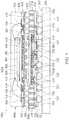
- FIG. 1 is a cross-sectional view of a semiconductor package assembly 500a including a hybrid system-on-chip (SOC) package 300a and a dynamic random access memory (DRAM) package 400a stacked thereon in accordance with some embodiments of the disclosure.
- the semiconductor package assembly 500a is a package-on-package (POP) semiconductor package assembly.
- the semiconductor package assembly 500a includes at least two vertically stacked wafer-level semiconductor packages mounted on a base 200.
- the vertically stacked wafer-level semiconductor packages include a hybrid system-on-chip (SOC) package 300a and a dynamic random access memory (DRAM) package 400a vertically stacked thereon.
- the base 200 for example a printed circuit board (PCB), may be formed of polypropylene (PP). It should also be noted that the base 200 can be a single layer or a multilayer structure.
- a plurality of pads (not shown) and/or conductive traces (not shown) is disposed on a die-attach surface 202 of the base 200.
- the conductive traces may comprise signal trace segments or ground trace segments, which are used for the input/output (I/O) connections of the SOC package 300a and the DRAM package 400a.
- the SOC package 300a is mounted directly on the conductive traces.
- the pads are disposed on the die-attach surface 202, connected to different terminals of the conductive traces. The pads are used for the SOC package 300a mounted directly thereon.
- the hybrid SOC package 300a is mounted on the die-attach surface 202 of the base 200 by a bonding process.
- the hybrid SOC package 300a is mounted on the base 200 through the conductive structures 322.
- the hybrid SOC package 300a is a three-dimensional (3D) semiconductor package including a system on chip (SOC) die 302, a dynamic random access memory (DRAM) die 600 and a redistribution layer (RDL) structure 316.
- the system on chip (SOC) die 302 may include a logic die including a central processing unit (CPU), a graphic processing unit (GPU), a dynamic random access memory (DRAM) controller or any combination thereof.
- the dynamic random access memory (DRAM) die 600 may include a Wide I/O DRAM die, vertically stacked on the SOC die 302.
- the DRAM die 600 of the hybrid SOC package 300a is fabricated by the through silicon via (TSV) technology.
- TSV through silicon via
- the SOC die 302 and the DRAM die 600 of the hybrid SOC package 300a are connected to each other and/or to the redistribution layer (RDL) structure 316 by vias (such as vias 308, 310).
- vias such as vias 308, 310. It should be noted that the number of SOC dies 302 and the number of DRAM dies 600 are not limited to the disclosed embodiment.
- the SOC die 302 has a back surface 302a and a front surface 302b.
- the SOC die 302 is fabricated by a flip-chip technology.
- the back surface 302a of the SOC die 302 is close to or aligned with the top surface 324 of the hybrid SOC package 300a.
- Pads 304 of the SOC die 302 are disposed on the front surface 302b to be electrically connected to the circuitry (not shown) of the SOC die 302.
- the pads 304 belong to the uppermost metal layer of the interconnection structure (not shown) of the SOC die 302.
- the pads 304 of the SOC die 302 are in contact with the corresponding vias 308.
- the DRAM die 600 is stacked on the front surface 302b of the SOC die 302.
- the DRAM die 600 is coupled to the pads 304 of the SOC die 302 through the vias 308 disposed on the SOC die 302.
- the DRAM die 600 may include TSV interconnects 602 formed through the DRAM die 600.
- the TSV interconnects 602 arranged as an array are used to transmit input/output (I/O), ground or power signals from the DRAM die 600 to the SOC die 302 and/or the base 200.
- the TSV interconnects 602 may be designed to follow the pin assignment rule (such as JEDEC Wide I/O Memory specification). It should be noted that the number of TSV interconnects in the array is defined by design for the DRAM die 600 and the SOC die 302 mounted thereon and the scope of the disclosure is not limited.
- the vias 308 are coupled to the TSV interconnects 602.
- the hybrid SOC package 300a further includes a molding compound 312 surrounding the SOC die 302 and the DRAM die 600, and filling any gaps around the SOC die 302 and the DRAM die 600.
- the molding compound 312 is in contact with the SOC die 302 and the DRAM die 600.
- the molded compound 312 also cover the top surface 302b of the SOC die 302.
- the molded compound 312 may be formed of a nonconductive material, such as an epoxy, a resin, a moldable polymer, or the like.
- the molding compound 312 may be applied while substantially liquid, and then may be cured through a chemical reaction, such as in an epoxy or resin.
- the molding compound 312 may be an ultraviolet (UV) or thermally cured polymer applied as a gel or malleable solid capable of being disposed around the SOC die 302 and the DRAM die 600, and then may be cured through a UV or thermally curing process.
- the molding compound 312 may be cured with a mold.
- the hybrid SOC package 300a further includes a redistribution layer (RDL) structure 316 is disposed on the DRAM die 600 and the SOC die 302, so that the DRAM die 600 is between the SOC die 302 and the RDL structure 316.
- the RDL structure 316 may be in contact with the molding compound 312 and the TSV interconnects 602 of the DRAM die 600.
- the RDL structure 316 may have one or more conductive traces 318 disposed in one or more intermetal dielectric (IMD) layers 317.
- IMD intermetal dielectric
- the conductive traces 318 are electrically connected to corresponding RDL contact pads 320.
- the RDL contact pads 320 are exposed to openings of the solder mask layer 321.
- the number of conductive traces 318, the number of IMD layers 317 and the number of RDL contact pads 320 shown in FIG. 1 is only an example and is not a limitation to the present invention.
- the hybrid SOC package 300a further includes conductive structures 322 disposed on a surface of the RDL structure 316 away from the DRAM die 600 and the SOC die 302.
- the conductive structures 322 are coupled to the conductive traces 318 through the RDL contact pads 320.
- the conductive structures 322 may comprise a conductive bump structure such as a copper bump or a solder bump structure, a conductive pillar structure, a conductive wire structure, or a conductive paste structure.
- the DRAM die 600 uses the TSV interconnects 602 respectively connecting the pads 304 of the SOC die 302 to the conductive traces 318 of the RDL structure 316 by the vias 308. Also, pads 306 of the SOC die 302 are coupled to the conductive traces 318 of the RDL structure 316 by vias 310 passing through the molding compound 312 between the SOC die 302 and the RDL structure 316. The DRAM die 600 is surrounded by the vias 310.
- the conductive traces 318 may be designed to be fan out from one or more of the pads 304 and 306 of the SOC die 302 and TSV interconnects 602 of DRAM die 600 to provide electrical connections between the SOC die 302, DRAM die 600 and the RDL contact pads 320. Therefore, the RDL contact pads 320 may have a larger bond pitch than the pads 304 and 306 of the SOC die 302 and TSV interconnects 602 of DRAM die 600, and which may be suitable for a ball grid array or another package mounting system.
- the DRAM package 400a is stacked on the hybrid SOC package 300a by a bonding process.
- the DRAM package 400a is a low-power double data rate DRAM (LPDDR DRAM) package following the pin assignment rule (such as JEDEC LPDDR I/O Memory specification).
- LPDDR DRAM low-power double data rate DRAM
- the DRAM package 400a includes a body 418 and at least one LPDDR DRAM die, for example, three LPDDR DRAM dies 402, 404 and 406, stacked thereon.
- the body 418 has a die-attach surface 420 and a bump-attach surface 422 opposite to the die-attach surface 420.
- the number of input/output (I/O) pins of Wide I/O DRAM die 600 is designed to be different from the number of input/output (I/O) pins of each of the LPDDR DRAM dies 402, 404 and 406. In one embodiment, the number of input/output (I/O) pins of Wide I/O DRAM die 600 is eight times greater than the number of input/output (I/O) pins of each of the LPDDR DRAM dies 402, 404 and 406. In this embodiment, as shown in FIG. 1 , there are three LPDDR DRAM dies 402, 404 and 406 mounted on the die-attach surface 420 of the body 418.
- the LPDDR DRAM die 404 is stacked on the LPDDR DRAM die 402 through a paste (not shown), and the LPDDR DRAM die 406 is stacked on the LPDDR DRAM die 404 through a paste (not shown).
- the LPDDR DRAM dies 402, 404 and 406 may be coupled to the body 418 by bonding wires, for example bonding wires 414 and 416.
- the number of stacked DRAM devices is not limited to the disclosed embodiment.
- the three LPDDR DRAM dies 402, 404 and 406 as shown in FIG. 1 can be arranged side by side. Therefore, the LPDDR DRAM dies 402, 404 and 406 are mounted on die-attach surface 420 of the body 418 by paste.
- the body 418 may comprise circuitry 428 and metal pads 424 and 426 and 430.
- the metal pads 424 and 426 are disposed on the top of the circuitry 428 close to the die-attach surface 420.
- the metal pads 430 are disposed on the bottom of the circuitry 428 close to the bump-attach surface 430.
- the circuitry 428 of the DRAM package 400a is interconnected with the conductive traces 318 of the RDL structure 316 via a plurality of conductive structures 432 disposed on the bump-attach surface 422 of the body 418.
- the conductive structures 432 may comprise a conductive bump structure such as a copper bump or a solder bump structure, a conductive pillar structure, a conductive wire structure, or a conductive paste structure.
- the DRAM package 400a is coupled to the conductive traces 318 of the RDL structure 316 by the vias 314 passing through the molding compound 312 between the DRAM package 400a and the RDL structure 316 of the hybrid SOC package 300a.
- the SOC die 302 and the DRAM die 600 are surrounded by the vias 314.
- the DRAM package 400a further includes a molding material 412 covering the die-attach surface 420 of the body 418, encapsulating the LPDDR DRAM dies 402, 404 and 406, the bonding wires 414 and 416.
- FIG. 2 is a cross-sectional view of a semiconductor package assembly 500b including a system-on-chip (SOC) package 300b and a hybrid dynamic random access memory (DRAM) package 400b stacked thereon.
- SOC system-on-chip
- DRAM dynamic random access memory
- the SOC package 300b is a semiconductor package including a system on chip (SOC) die 302 and a redistribution layer (RDL) structure 316.
- the SOC package 300b does not include any DRAM die integrated therein.
- the SOC die 302 of the SOC package 300b is connected to the redistribution layer (RDL) structure 316 by vias (such as vias 310).
- the pads 304 of the SOC die 302 are in contact with the corresponding vias 308. It should be noted that the number of SOC dies 302 is not limited to the disclosed embodiment.
- the hybrid DRAM package 400b is stacked on the SOC package 300b by the bonding process.
- the hybrid DRAM package 400b is a three-dimensional (3D) semiconductor package including a wire bonding DRAM package stacked on a TSV DRAM package.
- the hybrid DRAM package 400b is a LPDDR DRAM/Wide I/O DRAM hybrid package including LPDDR DRAM dies following a specific pin assignment rule (such as JEDEC LPDDR I/O Memory specification) and Wide I/O DRAM dies following another specific pin assignment rule (such as JEDEC Wide I/O Memory specification).
- the hybrid DRAM package 400b includes a body 418, at least one LPDDR DRAM die and at least one Wide I/O DRAM die stacked on the body 418.
- the LPDDR DRAM die 404 is stacked on the LPDDR DRAM die 402 through a paste (not shown), and the LPDDR DRAM die 406 is stacked on the LPDDR DRAM die 404 through a paste (not shown).
- the LPDDR DRAM dies 402, 404 and 406 may be coupled to the body 418 by bonding wires, for example bonding wires 414 and 416.
- the number of stacked LPDDR DRAM dies is not limited to the disclosed embodiment.
- the three LPDDR DRAM dies 402, 404 and 406 as shown in FIG. 1 can be arranged side by side. Therefore, the LPDDR DRAM dies 402, 404 and 406 are mounted on die-attach surface 420 of the body 418 by paste.
- the body 418 may comprise circuitry (not shown) and metal pads 424 and 426 and 430.
- the metal pads 424 and 426 are disposed on the top of the circuitry 428 close to the die-attach surface 420.
- the metal pads 430 are disposed on the bottom of the circuitry 428 close to the bump-attach surface 430.
- the hybrid DRAM package 400b further includes a molding material 412 covering the die-attach surface 420 of the body 418, encapsulating the LPDDR DRAM dies 402, 404 and 406, the bonding wires 414 and 416.
- the hybrid DRAM package 400b further includes at least one Wide I/O DRAM die, for example, two Wide I/O DRAM dies 600a and 600b, embedded therein.
- the Wide I/O DRAM dies 600a and 600b are arranged side by side.
- the Wide I/O DRAM dies 600a and 600b may include corresponding TSV interconnects 602a and 602b formed through the Wide I/O DRAM dies 600a and 600b, respectively.
- the TSV interconnects 602a and 602b arranged as an array are used to transmit input/output (I/O), ground or power signals from the Wide I/O DRAM dies 600a and 600b to the LPDDR DRAM dies 402, 404 and 406 and/or the base 200.
- the TSV interconnects 602a and 602b may be designed to follow the pin assignment rule (such as JEDEC Wide I/O Memory specification). It should be noted that the number of TSV interconnects in the array is defined by design for the Wide I/O DRAM dies 600a and 600b and the LPDDR DRAM dies 402, 404 and 406 mounted thereon and the scope of the disclosure is not limited.
- the TSV interconnects 602 are coupled to the metal pads 430 of the body 418.
- the number of input/output (I/O) pins of Wide I/O DRAM dies 600a and 600b are designed to be different from the number of input/output (I/O) pins of each of the LPDDR DRAM dies 402, 404 and 406.
- the number of input/output (I/O) pins of Wide I/O DRAM dies 600a and 600b are eight times greater than the number of input/output (I/O) pins of each of the LPDDR DRAM dies 402, 404 and 406.
- the hybrid DRAM package 400b further includes a molding compound 442 disposed on the bump-attach surface 422 of the body 418.
- the molding compound 442 surrounds the Wide I/O DRAM dies 600a and 600b, and filling any gaps around the Wide I/O DRAM dies 600a and 600b.
- the molding compound 442 is in contact with the Wide I/O DRAM dies 600a and 600b.
- the hybrid DRAM package 400b further includes a redistribution layer (RDL) structure 440 on the bump-attach surface 422 of the body 418.
- the RDL structure 440 is also disposed on the LPDDR DRAM dies 402, 404 and 406 and the Wide I/O DRAM dies 600a and 600b.
- the Wide I/O DRAM dies 600a and 600b is between the body 418 and the RDL structure 440.
- the RDL structure 440 may be in contact with the molding compound 442 and the TSV interconnects 602a and 602b of the DRAM dies 600a and 600b.
- the RDL structure 440 may have one or more conductive traces 448 disposed in one or more intermetal dielectric (IMD) layers 446.
- the conductive traces 448 are electrically connected to corresponding RDL contact pads 450.
- IMD intermetal dielectric
- the LPDDR DRAM dies 402, 404 and 406 may be coupled to the RDL contact pads 450 of the RDL structure 440 by vias 444 passing through the molding compound 442 between the molding compound 442 and the RDL structure 440.
- the Wide I/O DRAM dies 600a and 600b are surrounded by the vias 444.
- the conductive traces 448 of the DRAM package 400b is interconnected with the conductive traces 318 of the RDL structure 316 of the SOC package 300b via a plurality of conductive structures 452 disposed on the RDL contact pads 450 of the RDL structure 440.
- the conductive structures 452 may comprise a conductive bump structure such as a copper bump or a solder bump structure, a conductive pillar structure, a conductive wire structure, or a conductive paste structure.
- the conductive structures 452 of the DRAM package 400b are coupled to the RDL structure 316 of the SOC package 300b by the vias 314 passing through the molding compound 312 between the DRAM package 400b and the RDL structure 316 of the SOC package 300b.
- the SOC die 302 is surrounded by the vias 314.
- Embodiments provide semiconductor package assemblies 500a and 500b.
- Each of the semiconductor package assemblies 500a and 500b provides a LPDDR DRAM and Wide I/O DRAM hybrid memory integrated with a POP semiconductor package assembly.
- the POP semiconductor package assembly 500a includes a SOC/Wide I/O DRAM hybrid package 300a and a LPDDR DRAM package 400a stacked thereon.
- the POP semiconductor package assembly 500b includes a pure SOC package 300b and a LPDDR/Wide I/O DRAM hybrid package 400b stacked thereon.
- the semiconductor package assemblies 500a and 500b have advantages of the LPDDR DRAM package assembly (such as cost-effective, quick transition, and etc.) and the Wide I/O DRAM package assembly (such as high bandwidth, low power, etc.).
- the semiconductor package assemblies 500a and 500b may satisfy the requirements of cost-efficiency, high bandwidth, low power and quick transition.
Landscapes
- Engineering & Computer Science (AREA)
- Microelectronics & Electronic Packaging (AREA)
- Semiconductor Memories (AREA)
- Dram (AREA)
- Internal Circuitry In Semiconductor Integrated Circuit Devices (AREA)
- Semiconductor Integrated Circuits (AREA)
Claims (9)
- Ensemble semi-conducteur (500a) comprenant :un pack SOC (300a) comprenant :une matrice logique (302) comprenant des premiers blocs (304, 306) dessus ;une première structure RDL (316) couplée à la matrice logique (302) ; etun composé de moulage (312) entourant la matrice logique (302), en contact avec la première structure RDL (316) et la matrice logique (302) ; etun pack DRAM (400a, 400b) empilé sur le pack SOC (300a), comprenantun corps (418) comprenant une surface de fixation de matrice (420) et un surface de fixation à bosse (422) opposée à la surface de fixation de matrice (420) ; etune matrice DRAM (402, 404, 406) montée sur la surface de fixation de matrice (420), couplée au corps (418) par l'intermédiaire de fils de liaison (414, 416),le pack SOC (300a) comprenant en outre une matrice DRAM supplémentaire (600) intégrée,la matrice DRAM supplémentaire (600) comprenant des interconnexions TSV (602) formées à travers la matrice DRAM supplémentaire (600),la matrice logique (302) étant couplée à la première structure RDL (316) par des troisièmes passages (310) traversant le composé de moulage (312) entre la matrice logique (302) et la première structure RDL (316),la matrice DRAM supplémentaire (600) étant entourée par les troisièmes passages (310).
- Ensemble semi-conducteur selon la revendication 1, dans lequel un nombre de broches E/S de la matrice DRAM supplémentaire (600) est huit fois plus grand qu'un nombre de broches E/S de la matrice DRAM (402, 404, 406).
- Ensemble semi-conducteur selon la revendication 1 ou 2, dans lequel le pack SOC (300a) comprend des premiers passages (308) disposés sur la matrice logique (302), couplés aux premiers blocs (304).
- Ensemble semi-conducteur selon l'une des revendications précédentes, dans lequel le pack DRAM (400a) est couplé à la première structure RDL (316) du pack SOC (300a) par des deuxièmes passages (314) traversant le composé de moulage (312) entre le pack DRAM (400a) et la première structure RDL (316).
- Ensemble semi-conducteur selon l'une des revendications précédentes, dans lequel la matrice logique (302) est entourée par des deuxièmes passages (314).
- Ensemble semi-conducteur selon l'une des revendications précédentes, dans lequel la matrice DRAM supplémentaire (600) est couplée à des premiers passages (308) sur la matrice logique (302) et la première structure RDL (316).
- Ensemble semi-conducteur selon l'une des revendications précédentes, dans lequel le composé de moulage (312) est en contact avec la matrice DRAM supplémentaire (600).
- Ensemble semi-conducteur selon l'une des revendications précédentes, dans lequel le pack DRAM (400a) comprend :
une deuxième structure RDL disposée sur la surface de fixation à bosse (422). - Ensemble semi-conducteur selon l'une des revendications précédentes, comprenant en outre :
une base (200), le pack SOC (300a) et le pack DRAM (400a) étant montés sur la base (200) par l'intermédiaire de structures conductrices (322, 432).
Applications Claiming Priority (3)
| Application Number | Priority Date | Filing Date | Title |
|---|---|---|---|
| US201462050261P | 2014-09-15 | 2014-09-15 | |
| US201462058158P | 2014-10-01 | 2014-10-01 | |
| US14/741,796 US9548289B2 (en) | 2014-09-15 | 2015-06-17 | Semiconductor package assemblies with system-on-chip (SOC) packages |
Publications (2)
| Publication Number | Publication Date |
|---|---|
| EP2996146A1 EP2996146A1 (fr) | 2016-03-16 |
| EP2996146B1 true EP2996146B1 (fr) | 2020-02-19 |
Family
ID=53673851
Family Applications (1)
| Application Number | Title | Priority Date | Filing Date |
|---|---|---|---|
| EP15177483.3A Active EP2996146B1 (fr) | 2014-09-15 | 2015-07-20 | Assemblage de boîtiers semi-conducteurs |
Country Status (4)
| Country | Link |
|---|---|
| US (2) | US9548289B2 (fr) |
| EP (1) | EP2996146B1 (fr) |
| CN (1) | CN105428334B (fr) |
| TW (1) | TWI597815B (fr) |
Families Citing this family (45)
| Publication number | Priority date | Publication date | Assignee | Title |
|---|---|---|---|---|
| US20140264808A1 (en) * | 2013-03-15 | 2014-09-18 | Andreas Wolter | Chip arrangements, chip packages, and a method for manufacturing a chip arrangement |
| US9548289B2 (en) | 2014-09-15 | 2017-01-17 | Mediatek Inc. | Semiconductor package assemblies with system-on-chip (SOC) packages |
| US9633974B2 (en) * | 2015-03-04 | 2017-04-25 | Apple Inc. | System in package fan out stacking architecture and process flow |
| KR20160131170A (ko) | 2015-05-06 | 2016-11-16 | 에스케이하이닉스 주식회사 | 팬-아웃 메모리 패키지를 포함하는 패키지 온 패키지 타입의 반도체 장치 |
| US9418926B1 (en) | 2015-05-18 | 2016-08-16 | Micron Technology, Inc. | Package-on-package semiconductor assemblies and methods of manufacturing the same |
| KR20170026701A (ko) * | 2015-08-26 | 2017-03-09 | 삼성전자주식회사 | 반도체 칩, 이의 제조방법, 및 이를 포함하는 반도체 패키지 |
| KR20170044919A (ko) * | 2015-10-16 | 2017-04-26 | 삼성전자주식회사 | 반도체 패키지 및 이의 제조 방법 |
| US9761559B1 (en) | 2016-04-21 | 2017-09-12 | Micron Technology, Inc. | Semiconductor package and fabrication method thereof |
| CN105845672B (zh) * | 2016-06-15 | 2018-10-23 | 通富微电子股份有限公司 | 封装结构 |
| CN105957844B (zh) * | 2016-06-15 | 2018-07-27 | 通富微电子股份有限公司 | 封装结构 |
| CN105895541B (zh) * | 2016-06-15 | 2018-10-23 | 通富微电子股份有限公司 | 封装结构的形成方法 |
| CN105870024B (zh) * | 2016-06-15 | 2018-07-27 | 通富微电子股份有限公司 | 系统级封装方法 |
| US9859253B1 (en) * | 2016-06-29 | 2018-01-02 | Intel Corporation | Integrated circuit package stack |
| US10651116B2 (en) * | 2016-06-30 | 2020-05-12 | Intel Corporation | Planar integrated circuit package interconnects |
| US10790257B2 (en) | 2016-09-30 | 2020-09-29 | Intel Corporation | Active package substrate having anisotropic conductive layer |
| WO2018063384A1 (fr) * | 2016-09-30 | 2018-04-05 | Intel Corporation | Substrat de boîtier actif pourvu d'un interposeur intégré |
| US20180096975A1 (en) * | 2016-09-30 | 2018-04-05 | Intel Corporation | High density package on package devices created through a self assembly monolayer assisted laser direct structuring process on mold compound |
| US10163799B2 (en) * | 2016-11-07 | 2018-12-25 | Taiwan Semiconductor Manufacturing Company Ltd. | Semiconductor structure and method of manufacturing the same |
| US10014260B2 (en) * | 2016-11-10 | 2018-07-03 | Taiwan Semiconductor Manufacturing Co., Ltd. | Package structure and method for forming the same |
| US10410969B2 (en) * | 2017-02-15 | 2019-09-10 | Mediatek Inc. | Semiconductor package assembly |
| US10447274B2 (en) * | 2017-07-11 | 2019-10-15 | iCometrue Company Ltd. | Logic drive based on standard commodity FPGA IC chips using non-volatile memory cells |
| KR102450580B1 (ko) | 2017-12-22 | 2022-10-07 | 삼성전자주식회사 | 금속 배선 하부의 절연층 구조를 갖는 반도체 장치 |
| KR102482896B1 (ko) * | 2017-12-28 | 2022-12-30 | 삼성전자주식회사 | 이종 휘발성 메모리 칩들을 포함하는 메모리 장치 및 이를 포함하는 전자 장치 |
| US10510650B2 (en) * | 2018-02-02 | 2019-12-17 | Taiwan Semiconductor Manufacturing Company, Ltd. | Method of manufacturing semiconductor device packaging structure having through interposer vias and through substrate vias |
| KR102395199B1 (ko) | 2018-02-22 | 2022-05-06 | 삼성전자주식회사 | 반도체 패키지 |
| US10742217B2 (en) * | 2018-04-12 | 2020-08-11 | Apple Inc. | Systems and methods for implementing a scalable system |
| EP3867935A4 (fr) | 2018-10-18 | 2022-07-13 | Smoltek AB | Composant de stockage d'énergie métal-isolant-métal (mim) discret et procédé de fabrication |
| US12211863B2 (en) * | 2018-11-19 | 2025-01-28 | Utac Headquarters Pte Ltd. | Reliable semiconductor packages |
| US10770433B1 (en) | 2019-02-27 | 2020-09-08 | Apple Inc. | High bandwidth die to die interconnect with package area reduction |
| US10803548B2 (en) | 2019-03-15 | 2020-10-13 | Intel Corporation | Disaggregation of SOC architecture |
| KR102801218B1 (ko) | 2019-08-30 | 2025-04-29 | 삼성전자주식회사 | 디스플레이 모듈 패키지 |
| US11171121B2 (en) | 2020-03-31 | 2021-11-09 | Micron Technology, Inc. | Semiconductor devices with redistribution structures configured for switchable routing |
| US11723150B2 (en) * | 2020-09-04 | 2023-08-08 | Micron Technology, Inc. | Surface mount device bonded to an inner layer of a multi-layer substrate |
| US12512371B2 (en) * | 2021-06-28 | 2025-12-30 | Advanced Micro Devices, Inc. | Wafer-level testing of fanout chiplets |
| US12142544B2 (en) * | 2021-09-27 | 2024-11-12 | Samsung Electronics Co., Ltd. | Semiconductor package |
| US12230622B2 (en) * | 2021-10-13 | 2025-02-18 | Mediatek Inc. | Electronic device with stacked printed circuit boards |
| KR20230142126A (ko) | 2022-04-01 | 2023-10-11 | 삼성전자주식회사 | 반도체 패키지 |
| KR20230143014A (ko) * | 2022-04-04 | 2023-10-11 | 삼성전자주식회사 | 반도체 패키지 |
| CN114975415A (zh) * | 2022-04-29 | 2022-08-30 | 盛合晶微半导体(江阴)有限公司 | 扇出堆叠型半导体封装结构及其封装方法 |
| US20240071939A1 (en) * | 2022-08-28 | 2024-02-29 | Taiwan Semiconductor Manufacturing Company, Ltd. | Semiconductor structure and manufacturing method thereof |
| US20240206066A1 (en) * | 2022-12-20 | 2024-06-20 | Qualcomm Incorporated | Hybrid circuit board device to support circuit reuse and method of manufacture |
| KR20240117931A (ko) * | 2023-01-26 | 2024-08-02 | 삼성전자주식회사 | 반도체 패키지 및 그 제조 방법 |
| CN117334649A (zh) * | 2023-10-30 | 2024-01-02 | 展讯通信(上海)有限公司 | 混合垂直堆叠封装结构 |
| CN117457619B (zh) * | 2023-12-26 | 2024-04-05 | 北京奎芯集成电路设计有限公司 | 一种基于高带宽互联技术的半导体器件 |
| US20250385222A1 (en) * | 2024-06-13 | 2025-12-18 | Qualcomm Incorporated | High-bandwidth integrated circuit packaging of memory and logic |
Family Cites Families (26)
| Publication number | Priority date | Publication date | Assignee | Title |
|---|---|---|---|---|
| US20080029884A1 (en) * | 2006-08-03 | 2008-02-07 | Juergen Grafe | Multichip device and method for producing a multichip device |
| JP2010080801A (ja) | 2008-09-29 | 2010-04-08 | Hitachi Ltd | 半導体装置 |
| KR101461630B1 (ko) | 2008-11-06 | 2014-11-20 | 삼성전자주식회사 | 실장 높이는 축소되나, 솔더 접합 신뢰도는 개선되는 웨이퍼 레벨 칩 온 칩 패키지와, 패키지 온 패키지 및 그 제조방법 |
| US7867821B1 (en) * | 2009-09-18 | 2011-01-11 | Stats Chippac Ltd. | Integrated circuit package system with through semiconductor vias and method of manufacture thereof |
| US20110133327A1 (en) | 2009-12-09 | 2011-06-09 | Hung-Hsin Hsu | Semiconductor package of metal post solder-chip connection |
| US8564141B2 (en) * | 2010-05-06 | 2013-10-22 | SK Hynix Inc. | Chip unit and stack package having the same |
| KR101855294B1 (ko) * | 2010-06-10 | 2018-05-08 | 삼성전자주식회사 | 반도체 패키지 |
| JP5587123B2 (ja) | 2010-09-30 | 2014-09-10 | ルネサスエレクトロニクス株式会社 | 半導体装置の製造方法 |
| WO2012124830A1 (fr) * | 2011-03-17 | 2012-09-20 | 日本碍子株式会社 | Elément de modulation optique |
| US20130020699A1 (en) | 2011-07-06 | 2013-01-24 | Mediatek Inc. | Package structure and method for fabricating the same |
| WO2013017917A1 (fr) * | 2011-08-04 | 2013-02-07 | Sony Ericsson Mobile Communications Ab | Ensemble semi-conducteur |
| US8659144B1 (en) | 2011-12-15 | 2014-02-25 | Marvell International Ltd. | Power and ground planes in package substrate |
| US9484319B2 (en) | 2011-12-23 | 2016-11-01 | STATS ChipPAC Pte. Ltd. | Semiconductor device and method of forming extended semiconductor device with fan-out interconnect structure to reduce complexity of substrate |
| US9502360B2 (en) | 2012-01-11 | 2016-11-22 | Taiwan Semiconductor Manufacturing Company, Ltd. | Stress compensation layer for 3D packaging |
| US9881894B2 (en) * | 2012-03-08 | 2018-01-30 | STATS ChipPAC Pte. Ltd. | Thin 3D fan-out embedded wafer level package (EWLB) for application processor and memory integration |
| US9553040B2 (en) | 2012-03-27 | 2017-01-24 | Mediatek Inc. | Semiconductor package |
| US9009400B2 (en) * | 2012-10-16 | 2015-04-14 | Rambus Inc. | Semiconductor memory systems with on-die data buffering |
| US9263377B2 (en) | 2012-11-08 | 2016-02-16 | Taiwan Semiconductor Manufacturing Company, Ltd. | POP structures with dams encircling air gaps and methods for forming the same |
| US9378982B2 (en) | 2013-01-31 | 2016-06-28 | Taiwan Semiconductor Manufacturing Company, Ltd. | Die package with openings surrounding end-portions of through package vias (TPVs) and package on package (PoP) using the die package |
| US9331054B2 (en) * | 2013-03-14 | 2016-05-03 | Mediatek Inc. | Semiconductor package assembly with decoupling capacitor |
| US20140291834A1 (en) * | 2013-03-27 | 2014-10-02 | Micron Technology, Inc. | Semiconductor devices and packages including conductive underfill material and related methods |
| US9184128B2 (en) | 2013-12-13 | 2015-11-10 | Taiwan Semiconductor Manufacturing Company, Ltd. | 3DIC package and methods of forming the same |
| US9735129B2 (en) | 2014-03-21 | 2017-08-15 | Taiwan Semiconductor Manufacturing Company, Ltd. | Semiconductor packages and methods of forming the same |
| US9704739B2 (en) | 2014-07-30 | 2017-07-11 | Taiwan Semiconductor Manufacturing Company, Ltd. | Semiconductor device packages, packaging methods, and packaged semiconductor devices |
| US20160079205A1 (en) | 2014-09-15 | 2016-03-17 | Mediatek Inc. | Semiconductor package assembly |
| US9548289B2 (en) | 2014-09-15 | 2017-01-17 | Mediatek Inc. | Semiconductor package assemblies with system-on-chip (SOC) packages |
-
2015
- 2015-06-17 US US14/741,796 patent/US9548289B2/en active Active
- 2015-07-20 EP EP15177483.3A patent/EP2996146B1/fr active Active
- 2015-08-21 TW TW104127286A patent/TWI597815B/zh not_active IP Right Cessation
- 2015-09-14 CN CN201510582282.5A patent/CN105428334B/zh active Active
-
2016
- 2016-11-30 US US15/365,217 patent/US10361173B2/en active Active
Non-Patent Citations (1)
| Title |
|---|
| None * |
Also Published As
| Publication number | Publication date |
|---|---|
| US20170084583A1 (en) | 2017-03-23 |
| US9548289B2 (en) | 2017-01-17 |
| US20160079220A1 (en) | 2016-03-17 |
| EP2996146A1 (fr) | 2016-03-16 |
| TW201611233A (zh) | 2016-03-16 |
| US10361173B2 (en) | 2019-07-23 |
| TWI597815B (zh) | 2017-09-01 |
| CN105428334A (zh) | 2016-03-23 |
| CN105428334B (zh) | 2019-03-01 |
Similar Documents
| Publication | Publication Date | Title |
|---|---|---|
| EP2996146B1 (fr) | Assemblage de boîtiers semi-conducteurs | |
| US10332830B2 (en) | Semiconductor package assembly | |
| US10410969B2 (en) | Semiconductor package assembly | |
| US20160079205A1 (en) | Semiconductor package assembly | |
| EP2775512B1 (fr) | Dispositifs semi-conducteurs | |
| EP3163614B1 (fr) | Structure de boîtier de sortance empilé | |
| CN104064551B (zh) | 一种芯片堆叠封装结构和电子设备 | |
| US9978729B2 (en) | Semiconductor package assembly | |
| US10468341B2 (en) | Semiconductor package assembly | |
| EP3154083B1 (fr) | Structure de boîtier de sortance ayant un substrat de boîtier encastré | |
| US20160172292A1 (en) | Semiconductor package assembly | |
| CN105977220B (zh) | 半导体封装组件 | |
| CN105990326A (zh) | 半导体封装、半导体封装结构及制造半导体封装的方法 | |
| US20170141041A1 (en) | Semiconductor package assembly | |
| EP3073527A1 (fr) | Ensemble de boîtier de semi-conducteur | |
| US12368104B2 (en) | Electronic package |
Legal Events
| Date | Code | Title | Description |
|---|---|---|---|
| PUAI | Public reference made under article 153(3) epc to a published international application that has entered the european phase |
Free format text: ORIGINAL CODE: 0009012 |
|
| AK | Designated contracting states |
Kind code of ref document: A1 Designated state(s): AL AT BE BG CH CY CZ DE DK EE ES FI FR GB GR HR HU IE IS IT LI LT LU LV MC MK MT NL NO PL PT RO RS SE SI SK SM TR |
|
| AX | Request for extension of the european patent |
Extension state: BA ME |
|
| 17P | Request for examination filed |
Effective date: 20160901 |
|
| RBV | Designated contracting states (corrected) |
Designated state(s): AL AT BE BG CH CY CZ DE DK EE ES FI FR GB GR HR HU IE IS IT LI LT LU LV MC MK MT NL NO PL PT RO RS SE SI SK SM TR |
|
| STAA | Information on the status of an ep patent application or granted ep patent |
Free format text: STATUS: EXAMINATION IS IN PROGRESS |
|
| 17Q | First examination report despatched |
Effective date: 20180809 |
|
| RIC1 | Information provided on ipc code assigned before grant |
Ipc: H01L 25/065 20060101AFI20190723BHEP Ipc: H01L 23/00 20060101ALI20190723BHEP Ipc: H01L 23/31 20060101ALI20190723BHEP Ipc: H01L 23/50 20060101ALI20190723BHEP Ipc: H05K 1/11 20060101ALI20190723BHEP Ipc: H01L 25/10 20060101ALI20190723BHEP Ipc: H01L 23/48 20060101ALI20190723BHEP Ipc: H01L 25/18 20060101ALI20190723BHEP Ipc: H05K 1/18 20060101ALI20190723BHEP |
|
| GRAP | Despatch of communication of intention to grant a patent |
Free format text: ORIGINAL CODE: EPIDOSNIGR1 |
|
| STAA | Information on the status of an ep patent application or granted ep patent |
Free format text: STATUS: GRANT OF PATENT IS INTENDED |
|
| INTG | Intention to grant announced |
Effective date: 20190930 |
|
| GRAS | Grant fee paid |
Free format text: ORIGINAL CODE: EPIDOSNIGR3 |
|
| GRAA | (expected) grant |
Free format text: ORIGINAL CODE: 0009210 |
|
| STAA | Information on the status of an ep patent application or granted ep patent |
Free format text: STATUS: THE PATENT HAS BEEN GRANTED |
|
| AK | Designated contracting states |
Kind code of ref document: B1 Designated state(s): AL AT BE BG CH CY CZ DE DK EE ES FI FR GB GR HR HU IE IS IT LI LT LU LV MC MK MT NL NO PL PT RO RS SE SI SK SM TR |
|
| REG | Reference to a national code |
Ref country code: CH Ref legal event code: EP |
|
| REG | Reference to a national code |
Ref country code: DE Ref legal event code: R096 Ref document number: 602015047177 Country of ref document: DE |
|
| REG | Reference to a national code |
Ref country code: AT Ref legal event code: REF Ref document number: 1235933 Country of ref document: AT Kind code of ref document: T Effective date: 20200315 |
|
| REG | Reference to a national code |
Ref country code: IE Ref legal event code: FG4D |
|
| REG | Reference to a national code |
Ref country code: NL Ref legal event code: MP Effective date: 20200219 |
|
| PG25 | Lapsed in a contracting state [announced via postgrant information from national office to epo] |
Ref country code: NO Free format text: LAPSE BECAUSE OF FAILURE TO SUBMIT A TRANSLATION OF THE DESCRIPTION OR TO PAY THE FEE WITHIN THE PRESCRIBED TIME-LIMIT Effective date: 20200519 Ref country code: RS Free format text: LAPSE BECAUSE OF FAILURE TO SUBMIT A TRANSLATION OF THE DESCRIPTION OR TO PAY THE FEE WITHIN THE PRESCRIBED TIME-LIMIT Effective date: 20200219 Ref country code: FI Free format text: LAPSE BECAUSE OF FAILURE TO SUBMIT A TRANSLATION OF THE DESCRIPTION OR TO PAY THE FEE WITHIN THE PRESCRIBED TIME-LIMIT Effective date: 20200219 |
|
| REG | Reference to a national code |
Ref country code: LT Ref legal event code: MG4D |
|
| PG25 | Lapsed in a contracting state [announced via postgrant information from national office to epo] |
Ref country code: GR Free format text: LAPSE BECAUSE OF FAILURE TO SUBMIT A TRANSLATION OF THE DESCRIPTION OR TO PAY THE FEE WITHIN THE PRESCRIBED TIME-LIMIT Effective date: 20200520 Ref country code: IS Free format text: LAPSE BECAUSE OF FAILURE TO SUBMIT A TRANSLATION OF THE DESCRIPTION OR TO PAY THE FEE WITHIN THE PRESCRIBED TIME-LIMIT Effective date: 20200619 Ref country code: HR Free format text: LAPSE BECAUSE OF FAILURE TO SUBMIT A TRANSLATION OF THE DESCRIPTION OR TO PAY THE FEE WITHIN THE PRESCRIBED TIME-LIMIT Effective date: 20200219 Ref country code: LV Free format text: LAPSE BECAUSE OF FAILURE TO SUBMIT A TRANSLATION OF THE DESCRIPTION OR TO PAY THE FEE WITHIN THE PRESCRIBED TIME-LIMIT Effective date: 20200219 Ref country code: SE Free format text: LAPSE BECAUSE OF FAILURE TO SUBMIT A TRANSLATION OF THE DESCRIPTION OR TO PAY THE FEE WITHIN THE PRESCRIBED TIME-LIMIT Effective date: 20200219 Ref country code: BG Free format text: LAPSE BECAUSE OF FAILURE TO SUBMIT A TRANSLATION OF THE DESCRIPTION OR TO PAY THE FEE WITHIN THE PRESCRIBED TIME-LIMIT Effective date: 20200519 |
|
| PG25 | Lapsed in a contracting state [announced via postgrant information from national office to epo] |
Ref country code: NL Free format text: LAPSE BECAUSE OF FAILURE TO SUBMIT A TRANSLATION OF THE DESCRIPTION OR TO PAY THE FEE WITHIN THE PRESCRIBED TIME-LIMIT Effective date: 20200219 |
|
| PG25 | Lapsed in a contracting state [announced via postgrant information from national office to epo] |
Ref country code: LT Free format text: LAPSE BECAUSE OF FAILURE TO SUBMIT A TRANSLATION OF THE DESCRIPTION OR TO PAY THE FEE WITHIN THE PRESCRIBED TIME-LIMIT Effective date: 20200219 Ref country code: EE Free format text: LAPSE BECAUSE OF FAILURE TO SUBMIT A TRANSLATION OF THE DESCRIPTION OR TO PAY THE FEE WITHIN THE PRESCRIBED TIME-LIMIT Effective date: 20200219 Ref country code: SM Free format text: LAPSE BECAUSE OF FAILURE TO SUBMIT A TRANSLATION OF THE DESCRIPTION OR TO PAY THE FEE WITHIN THE PRESCRIBED TIME-LIMIT Effective date: 20200219 Ref country code: DK Free format text: LAPSE BECAUSE OF FAILURE TO SUBMIT A TRANSLATION OF THE DESCRIPTION OR TO PAY THE FEE WITHIN THE PRESCRIBED TIME-LIMIT Effective date: 20200219 Ref country code: ES Free format text: LAPSE BECAUSE OF FAILURE TO SUBMIT A TRANSLATION OF THE DESCRIPTION OR TO PAY THE FEE WITHIN THE PRESCRIBED TIME-LIMIT Effective date: 20200219 Ref country code: RO Free format text: LAPSE BECAUSE OF FAILURE TO SUBMIT A TRANSLATION OF THE DESCRIPTION OR TO PAY THE FEE WITHIN THE PRESCRIBED TIME-LIMIT Effective date: 20200219 Ref country code: CZ Free format text: LAPSE BECAUSE OF FAILURE TO SUBMIT A TRANSLATION OF THE DESCRIPTION OR TO PAY THE FEE WITHIN THE PRESCRIBED TIME-LIMIT Effective date: 20200219 Ref country code: PT Free format text: LAPSE BECAUSE OF FAILURE TO SUBMIT A TRANSLATION OF THE DESCRIPTION OR TO PAY THE FEE WITHIN THE PRESCRIBED TIME-LIMIT Effective date: 20200712 Ref country code: SK Free format text: LAPSE BECAUSE OF FAILURE TO SUBMIT A TRANSLATION OF THE DESCRIPTION OR TO PAY THE FEE WITHIN THE PRESCRIBED TIME-LIMIT Effective date: 20200219 |
|
| REG | Reference to a national code |
Ref country code: AT Ref legal event code: MK05 Ref document number: 1235933 Country of ref document: AT Kind code of ref document: T Effective date: 20200219 |
|
| REG | Reference to a national code |
Ref country code: DE Ref legal event code: R097 Ref document number: 602015047177 Country of ref document: DE |
|
| PLBE | No opposition filed within time limit |
Free format text: ORIGINAL CODE: 0009261 |
|
| STAA | Information on the status of an ep patent application or granted ep patent |
Free format text: STATUS: NO OPPOSITION FILED WITHIN TIME LIMIT |
|
| 26N | No opposition filed |
Effective date: 20201120 |
|
| PG25 | Lapsed in a contracting state [announced via postgrant information from national office to epo] |
Ref country code: IT Free format text: LAPSE BECAUSE OF FAILURE TO SUBMIT A TRANSLATION OF THE DESCRIPTION OR TO PAY THE FEE WITHIN THE PRESCRIBED TIME-LIMIT Effective date: 20200219 Ref country code: AT Free format text: LAPSE BECAUSE OF FAILURE TO SUBMIT A TRANSLATION OF THE DESCRIPTION OR TO PAY THE FEE WITHIN THE PRESCRIBED TIME-LIMIT Effective date: 20200219 |
|
| PG25 | Lapsed in a contracting state [announced via postgrant information from national office to epo] |
Ref country code: MC Free format text: LAPSE BECAUSE OF FAILURE TO SUBMIT A TRANSLATION OF THE DESCRIPTION OR TO PAY THE FEE WITHIN THE PRESCRIBED TIME-LIMIT Effective date: 20200219 Ref country code: PL Free format text: LAPSE BECAUSE OF FAILURE TO SUBMIT A TRANSLATION OF THE DESCRIPTION OR TO PAY THE FEE WITHIN THE PRESCRIBED TIME-LIMIT Effective date: 20200219 Ref country code: SI Free format text: LAPSE BECAUSE OF FAILURE TO SUBMIT A TRANSLATION OF THE DESCRIPTION OR TO PAY THE FEE WITHIN THE PRESCRIBED TIME-LIMIT Effective date: 20200219 |
|
| REG | Reference to a national code |
Ref country code: CH Ref legal event code: PL |
|
| REG | Reference to a national code |
Ref country code: BE Ref legal event code: MM Effective date: 20200731 |
|
| PG25 | Lapsed in a contracting state [announced via postgrant information from national office to epo] |
Ref country code: CH Free format text: LAPSE BECAUSE OF NON-PAYMENT OF DUE FEES Effective date: 20200731 Ref country code: LI Free format text: LAPSE BECAUSE OF NON-PAYMENT OF DUE FEES Effective date: 20200731 Ref country code: LU Free format text: LAPSE BECAUSE OF NON-PAYMENT OF DUE FEES Effective date: 20200720 |
|
| PG25 | Lapsed in a contracting state [announced via postgrant information from national office to epo] |
Ref country code: BE Free format text: LAPSE BECAUSE OF NON-PAYMENT OF DUE FEES Effective date: 20200731 |
|
| PG25 | Lapsed in a contracting state [announced via postgrant information from national office to epo] |
Ref country code: IE Free format text: LAPSE BECAUSE OF NON-PAYMENT OF DUE FEES Effective date: 20200720 |
|
| PG25 | Lapsed in a contracting state [announced via postgrant information from national office to epo] |
Ref country code: TR Free format text: LAPSE BECAUSE OF FAILURE TO SUBMIT A TRANSLATION OF THE DESCRIPTION OR TO PAY THE FEE WITHIN THE PRESCRIBED TIME-LIMIT Effective date: 20200219 Ref country code: MT Free format text: LAPSE BECAUSE OF FAILURE TO SUBMIT A TRANSLATION OF THE DESCRIPTION OR TO PAY THE FEE WITHIN THE PRESCRIBED TIME-LIMIT Effective date: 20200219 Ref country code: CY Free format text: LAPSE BECAUSE OF FAILURE TO SUBMIT A TRANSLATION OF THE DESCRIPTION OR TO PAY THE FEE WITHIN THE PRESCRIBED TIME-LIMIT Effective date: 20200219 |
|
| PG25 | Lapsed in a contracting state [announced via postgrant information from national office to epo] |
Ref country code: MK Free format text: LAPSE BECAUSE OF FAILURE TO SUBMIT A TRANSLATION OF THE DESCRIPTION OR TO PAY THE FEE WITHIN THE PRESCRIBED TIME-LIMIT Effective date: 20200219 Ref country code: AL Free format text: LAPSE BECAUSE OF FAILURE TO SUBMIT A TRANSLATION OF THE DESCRIPTION OR TO PAY THE FEE WITHIN THE PRESCRIBED TIME-LIMIT Effective date: 20200219 |
|
| P01 | Opt-out of the competence of the unified patent court (upc) registered |
Effective date: 20230607 |
|
| REG | Reference to a national code |
Ref country code: DE Ref legal event code: R079 Ref document number: 602015047177 Country of ref document: DE Free format text: PREVIOUS MAIN CLASS: H01L0025065000 Ipc: H10D0080300000 |
|
| PGFP | Annual fee paid to national office [announced via postgrant information from national office to epo] |
Ref country code: GB Payment date: 20250529 Year of fee payment: 11 |
|
| PGFP | Annual fee paid to national office [announced via postgrant information from national office to epo] |
Ref country code: FR Payment date: 20250508 Year of fee payment: 11 |
|
| PGFP | Annual fee paid to national office [announced via postgrant information from national office to epo] |
Ref country code: DE Payment date: 20250528 Year of fee payment: 11 |