EP2996150A2 - Bildsensor mit farbfilterisolierschicht und verfahren zur herstellung davon - Google Patents
Bildsensor mit farbfilterisolierschicht und verfahren zur herstellung davon Download PDFInfo
- Publication number
- EP2996150A2 EP2996150A2 EP15180905.0A EP15180905A EP2996150A2 EP 2996150 A2 EP2996150 A2 EP 2996150A2 EP 15180905 A EP15180905 A EP 15180905A EP 2996150 A2 EP2996150 A2 EP 2996150A2
- Authority
- EP
- European Patent Office
- Prior art keywords
- color filters
- light
- color filter
- color
- light sensing
- Prior art date
- Legal status (The legal status is an assumption and is not a legal conclusion. Google has not performed a legal analysis and makes no representation as to the accuracy of the status listed.)
- Granted
Links
Images


Classifications
-
- G—PHYSICS
- G01—MEASURING; TESTING
- G01J—MEASUREMENT OF INTENSITY, VELOCITY, SPECTRAL CONTENT, POLARISATION, PHASE OR PULSE CHARACTERISTICS OF INFRARED, VISIBLE OR ULTRAVIOLET LIGHT; COLORIMETRY; RADIATION PYROMETRY
- G01J1/00—Photometry, e.g. photographic exposure meter
- G01J1/02—Details
- G01J1/04—Optical or mechanical part supplementary adjustable parts
- G01J1/0488—Optical or mechanical part supplementary adjustable parts with spectral filtering
- G01J1/0492—Optical or mechanical part supplementary adjustable parts with spectral filtering using at least two different filters
-
- B—PERFORMING OPERATIONS; TRANSPORTING
- B32—LAYERED PRODUCTS
- B32B—LAYERED PRODUCTS, i.e. PRODUCTS BUILT-UP OF STRATA OF FLAT OR NON-FLAT, e.g. CELLULAR OR HONEYCOMB, FORM
- B32B38/00—Ancillary operations in connection with laminating processes
-
- G—PHYSICS
- G02—OPTICS
- G02B—OPTICAL ELEMENTS, SYSTEMS OR APPARATUS
- G02B5/00—Optical elements other than lenses
- G02B5/20—Filters
- G02B5/201—Filters in the form of arrays
-
- H—ELECTRICITY
- H10—SEMICONDUCTOR DEVICES; ELECTRIC SOLID-STATE DEVICES NOT OTHERWISE PROVIDED FOR
- H10F—INORGANIC SEMICONDUCTOR DEVICES SENSITIVE TO INFRARED RADIATION, LIGHT, ELECTROMAGNETIC RADIATION OF SHORTER WAVELENGTH OR CORPUSCULAR RADIATION
- H10F39/00—Integrated devices, or assemblies of multiple devices, comprising at least one element covered by group H10F30/00, e.g. radiation detectors comprising photodiode arrays
- H10F39/011—Manufacture or treatment of image sensors covered by group H10F39/12
- H10F39/024—Manufacture or treatment of image sensors covered by group H10F39/12 of coatings or optical elements
-
- H—ELECTRICITY
- H10—SEMICONDUCTOR DEVICES; ELECTRIC SOLID-STATE DEVICES NOT OTHERWISE PROVIDED FOR
- H10F—INORGANIC SEMICONDUCTOR DEVICES SENSITIVE TO INFRARED RADIATION, LIGHT, ELECTROMAGNETIC RADIATION OF SHORTER WAVELENGTH OR CORPUSCULAR RADIATION
- H10F39/00—Integrated devices, or assemblies of multiple devices, comprising at least one element covered by group H10F30/00, e.g. radiation detectors comprising photodiode arrays
- H10F39/80—Constructional details of image sensors
- H10F39/805—Coatings
- H10F39/8053—Colour filters
-
- H—ELECTRICITY
- H10—SEMICONDUCTOR DEVICES; ELECTRIC SOLID-STATE DEVICES NOT OTHERWISE PROVIDED FOR
- H10F—INORGANIC SEMICONDUCTOR DEVICES SENSITIVE TO INFRARED RADIATION, LIGHT, ELECTROMAGNETIC RADIATION OF SHORTER WAVELENGTH OR CORPUSCULAR RADIATION
- H10F39/00—Integrated devices, or assemblies of multiple devices, comprising at least one element covered by group H10F30/00, e.g. radiation detectors comprising photodiode arrays
- H10F39/80—Constructional details of image sensors
- H10F39/806—Optical elements or arrangements associated with the image sensors
- H10F39/8067—Reflectors
-
- B—PERFORMING OPERATIONS; TRANSPORTING
- B32—LAYERED PRODUCTS
- B32B—LAYERED PRODUCTS, i.e. PRODUCTS BUILT-UP OF STRATA OF FLAT OR NON-FLAT, e.g. CELLULAR OR HONEYCOMB, FORM
- B32B2307/00—Properties of the layers or laminate
- B32B2307/40—Properties of the layers or laminate having particular optical properties
-
- H—ELECTRICITY
- H10—SEMICONDUCTOR DEVICES; ELECTRIC SOLID-STATE DEVICES NOT OTHERWISE PROVIDED FOR
- H10F—INORGANIC SEMICONDUCTOR DEVICES SENSITIVE TO INFRARED RADIATION, LIGHT, ELECTROMAGNETIC RADIATION OF SHORTER WAVELENGTH OR CORPUSCULAR RADIATION
- H10F39/00—Integrated devices, or assemblies of multiple devices, comprising at least one element covered by group H10F30/00, e.g. radiation detectors comprising photodiode arrays
- H10F39/80—Constructional details of image sensors
- H10F39/806—Optical elements or arrangements associated with the image sensors
- H10F39/8063—Microlenses
Definitions
- Apparatuses and methods consistent with exemplary embodiments relate to image sensors and methods of manufacturing the same, and more particularly, to image sensors including a color filter isolation layer capable of preventing crosstalk and loss of light in a peripheral portion of the image sensors and methods of manufacturing the image sensors.
- the image sensor may further include a color separation element that is disposed opposite the first color filter and configured to transmit light of the first wavelength band to the first color filter and to refract or diffract light in the second and third wavelength bands toward the second and third color filters.
- a color separation element that is disposed opposite the first color filter and configured to transmit light of the first wavelength band to the first color filter and to refract or diffract light in the second and third wavelength bands toward the second and third color filters.
- a distance between bottom surfaces of the second and third color filters and the light sensing layer may be greater than a distance between a bottom surface of the first color filter and the light sensing layer, and a distance between light incident surfaces of the second and third color filters and the light sensing layer may be greater than a distance between a light incident surface of the first color filter and the light sensing layer.
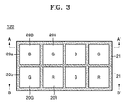
- the red color filter 20R, the green color filter 20G, and the blue color filter 20B are arranged in this order in FIG. 1 , the order is merely exemplary and the arrangement of the color filters is not limited thereto.
- the red color filter 20R, the green color filter 20G, and the blue color filter 20B, of the color filter layer 20 according to the present embodiment are also exemplary, and the color filter layer 20 may also include color filters of other colors.
- the color filter layer 20 may include cyan, yellow, green, and magenta color filters.
- filters which transmit other wavelength bands, including an infrared wavelength band, or an ultraviolet wavelength band may be used.
- the specifically-described colors and arrangement orders of the color filters of the color filter layer 20 are merely exemplary for convenience of description.
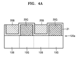
- FIG. 4A is a cross-sectional view of the first pixel row 120a of the image sensor 120 of FIG. 3 cut along a line A-A'.
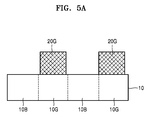
- a plurality of blue color filters 20B and a plurality of green color filters 20G are alternately arranged on the light sensing layer 10.
- the blue color filters 20B and the green color filters 20G may be respectively disposed on corresponding blue light sensing cells 10B and corresponding green light sensing cells 10G.
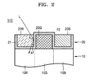
- the isolation layer 21 may extend between the blue color filter 20B and the light sensing layer 10, between the blue color filter 20B and the green color filter 20G, and on a light incident surface of the green color filter 20G.
- a distance between the bottom surface of the red color filter 20R and the light sensing layer 10 is greater than a distance between a bottom surface of the green color filter 20G and the light sensing layer 10.
- a distance between the light incident surface of the red color filter 20R and the light sensing layer 10 may be the same as a distance between the light incident surface of the green color filter 20G and the light sensing layer 10. Accordingly, a thickness of the red color filter 20R may be smaller than a thickness of the green color filter 20G by an amount equal to a thickness of the isolation layer 21 on the light sensing layer 10.
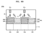
- the second pixel row 120b illustrated in FIG. 6B includes a plurality of green color filters 20G and a plurality of red color filters 20R that are alternately arranged.
- the isolation layer 21 may extend on a light incident surface of the green color filter 20G, between the green color filter 20G and the red color filter 20R, and between the red color filter 20R and the light sensing layer 10.
- an amount of light that is transmitted through the respective color filters 20G, 20R, and 20B increases, and thus, a light utilization efficiency of an image sensor may be improved.
- light separated by using the color separation element 30 may be used more efficiently.
- Light that is separated by using the color separation element 30 and is incident on the color filters 20G, 20R, and 20B proceeds approximately obliquely.
- the isolation layer 21 may totally internally reflect the light that proceeds obliquely in the color filters 20G, 20R, and 20B to thereby prevent incidence of light on other adjacent light sensing cells 10R, 10G, and 10B.
- a light utilization efficiency and color purity of an image sensor and may be simultaneously improved.
- the first color separation element 31a and the second color separation element 31b may be buried in the transparent dielectric layer 25, such that they are in fixed positions. Also, the first color separation element 31a may be disposed opposite the green color filter 20G of the first pixel row 150a, and the second color separation element 31b may be disposed opposite the green color filter 20G of the second pixel row 150b, as shown. In the above-described structure, the first color separation element 31a may be configured to transmit light C2 of a green wavelength band to the green color filter 20G, which is right below the first color separation element 31a, and to refract or diffract light C3 of a blue wavelength band toward the blue color filters 20B on the left and the right.
- 'R' and 'B' respectively denote spectrum distributions of light incident on the red and blue light sensing cells 10R and 10B when the first and second color separation elements 31a and 31b are used
- 'Gb' and 'Gr' respectively denote spectrum distributions of light incident on the green light sensing cell 10G of the first pixel row 150a and the green light sensing cell 10G of the second pixel row 150b when the first and second color separation elements 31a and 31b are used.
- a light utilization efficiency may be improved as compared to when just the color filters 20G, 20R, and 20B are used.
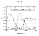
- FIG. 10 is a graph showing an exemplary spectrum distribution of light absorbed by light sensing cells 10R, 10G, and 10B of an image sensor according to a comparative example.
- the image sensor according to the comparative example has almost the same structure as the image sensors 150a and 150b illustrated in FIGS. 8A and 8B except that the isolation layer 21 is not included. That is, in the image sensor according to the comparative example, the color filters 20G, 20R, and 20B and the first and second color separation elements 31a and 31b are included but the isolation layer 21 is not disposed between the color filters 20G, 20R, and 20B. Referring to the graph of FIG.
Landscapes
- Physics & Mathematics (AREA)
- General Physics & Mathematics (AREA)
- Spectroscopy & Molecular Physics (AREA)
- Optics & Photonics (AREA)
- Solid State Image Pick-Up Elements (AREA)
Priority Applications (1)
| Application Number | Priority Date | Filing Date | Title |
|---|---|---|---|
| EP20162436.8A EP3696856B1 (de) | 2014-08-18 | 2015-08-13 | Bildsensor mit farbfilterisolierschicht und verfahren zur herstellung davon |
Applications Claiming Priority (1)
| Application Number | Priority Date | Filing Date | Title |
|---|---|---|---|
| KR1020140106964A KR102299714B1 (ko) | 2014-08-18 | 2014-08-18 | 컬러 필터 격리층을 구비하는 이미지 센서 및 상기 이미지 센서의 제조 방법 |
Related Child Applications (1)
| Application Number | Title | Priority Date | Filing Date |
|---|---|---|---|
| EP20162436.8A Division EP3696856B1 (de) | 2014-08-18 | 2015-08-13 | Bildsensor mit farbfilterisolierschicht und verfahren zur herstellung davon |
Publications (3)
| Publication Number | Publication Date |
|---|---|
| EP2996150A2 true EP2996150A2 (de) | 2016-03-16 |
| EP2996150A3 EP2996150A3 (de) | 2016-06-22 |
| EP2996150B1 EP2996150B1 (de) | 2020-03-18 |
Family
ID=53835973
Family Applications (2)
| Application Number | Title | Priority Date | Filing Date |
|---|---|---|---|
| EP15180905.0A Active EP2996150B1 (de) | 2014-08-18 | 2015-08-13 | Bildsensor mit farbfilterisolierschicht und verfahren zur herstellung davon |
| EP20162436.8A Active EP3696856B1 (de) | 2014-08-18 | 2015-08-13 | Bildsensor mit farbfilterisolierschicht und verfahren zur herstellung davon |
Family Applications After (1)
| Application Number | Title | Priority Date | Filing Date |
|---|---|---|---|
| EP20162436.8A Active EP3696856B1 (de) | 2014-08-18 | 2015-08-13 | Bildsensor mit farbfilterisolierschicht und verfahren zur herstellung davon |
Country Status (3)
| Country | Link |
|---|---|
| US (2) | US9863804B2 (de) |
| EP (2) | EP2996150B1 (de) |
| KR (1) | KR102299714B1 (de) |
Cited By (3)
| Publication number | Priority date | Publication date | Assignee | Title |
|---|---|---|---|---|
| CN109445164A (zh) * | 2018-09-30 | 2019-03-08 | 武汉天马微电子有限公司 | 一种显示面板及显示装置 |
| EP3499279A1 (de) * | 2017-12-18 | 2019-06-19 | Viavi Solutions Inc. | Optische filter |
| EP4546993A1 (de) * | 2016-08-31 | 2025-04-30 | LG Display Co., Ltd. | Anzeigevorrichtung und verfahren zur herstellung davon |
Families Citing this family (10)
| Publication number | Priority date | Publication date | Assignee | Title |
|---|---|---|---|---|
| JP2017208585A (ja) * | 2014-09-30 | 2017-11-24 | 株式会社ニコン | 撮像装置および画像データ生成プログラム |
| US10612976B1 (en) * | 2015-10-06 | 2020-04-07 | J.A. Woollan Co., Inc. | Systems and methods for producing a more uniform intensity wavelength dispersed beam of electromagnetic radiation entering a multi-element detector, while maintaining information content therein |
| JP6707418B2 (ja) * | 2016-08-05 | 2020-06-10 | 株式会社ジャパンディスプレイ | 表示装置、表示装置の製造方法、及び、カラーフィルタ基板 |
| US9880330B1 (en) * | 2016-09-06 | 2018-01-30 | Abeam Technologies, Inc. | Angle-insensitive spectral filter |
| US10103194B2 (en) * | 2016-09-26 | 2018-10-16 | Omnivision Technologies, Inc. | Self-aligned optical grid on image sensor |
| CN110767732B (zh) * | 2019-10-31 | 2022-04-05 | 昆山国显光电有限公司 | 显示装置 |
| KR102819914B1 (ko) | 2020-10-15 | 2025-06-13 | 삼성디스플레이 주식회사 | 표시 장치 |
| KR102660012B1 (ko) * | 2021-06-14 | 2024-04-23 | (재)한국나노기술원 | 광 센서 패키지 및 어레이 장치 |
| US12604550B2 (en) * | 2022-07-14 | 2026-04-14 | Visera Technologies Company Limited | Image sensor and method for reducing image signal processor |
| US20240274634A1 (en) * | 2023-02-14 | 2024-08-15 | Visera Technologies Company Ltd. | Image sensor |
Family Cites Families (23)
| Publication number | Priority date | Publication date | Assignee | Title |
|---|---|---|---|---|
| US7569804B2 (en) * | 2006-08-30 | 2009-08-04 | Dongbu Hitek Co., Ltd. | Image sensor having exposed dielectric layer in a region corresponding to a first color filter by a passivation layer |
| US20080204580A1 (en) * | 2007-02-28 | 2008-08-28 | Micron Technology, Inc. | Method, apparatus and system providing imaging device with color filter array |
| JP2009080313A (ja) * | 2007-09-26 | 2009-04-16 | Fujifilm Corp | カラーフィルタ、その製造方法、これを用いた固体撮像素子、およびその製造方法 |
| JP2009111225A (ja) * | 2007-10-31 | 2009-05-21 | Fujifilm Corp | 固体撮像素子及びその製造方法 |
| US8384818B2 (en) | 2008-06-18 | 2013-02-26 | Panasonic Corporation | Solid-state imaging device including arrays of optical elements and photosensitive cells |
| JP2010034141A (ja) * | 2008-07-25 | 2010-02-12 | Panasonic Corp | 固体撮像装置とその製造方法 |
| CN101816184B (zh) | 2008-08-05 | 2013-06-12 | 松下电器产业株式会社 | 摄像用光检测装置 |
| JP5331107B2 (ja) | 2008-12-19 | 2013-10-30 | パナソニック株式会社 | 撮像装置 |
| WO2010082455A1 (ja) | 2009-01-14 | 2010-07-22 | パナソニック株式会社 | 撮像装置 |
| EP2221606A3 (de) | 2009-02-11 | 2012-06-06 | Samsung Electronics Co., Ltd. | Integrierter Biochip und Verfahren zur Herstellung des integrierten Biochips |
| KR101563158B1 (ko) | 2009-02-11 | 2015-10-27 | 삼성전자주식회사 | 집적된 바이오칩 및 이의 제조방법 |
| JP4741015B2 (ja) | 2009-03-27 | 2011-08-03 | 富士フイルム株式会社 | 撮像素子 |
| JP2010272654A (ja) | 2009-05-20 | 2010-12-02 | Panasonic Corp | 固体撮像装置およびその製造方法 |
| JP2011119445A (ja) * | 2009-12-03 | 2011-06-16 | Toshiba Corp | 裏面照射型固体撮像装置 |
| JP5430387B2 (ja) * | 2009-12-22 | 2014-02-26 | キヤノン株式会社 | 固体撮像装置及び固体撮像装置の製造方法 |
| JP5503459B2 (ja) * | 2010-08-24 | 2014-05-28 | パナソニック株式会社 | 固体撮像素子および撮像装置 |
| JP5503458B2 (ja) | 2010-08-24 | 2014-05-28 | パナソニック株式会社 | 固体撮像素子および撮像装置 |
| JP2012074521A (ja) * | 2010-09-28 | 2012-04-12 | Sony Corp | 固体撮像装置の製造方法、固体撮像装置、および電子機器 |
| JP5736755B2 (ja) * | 2010-12-09 | 2015-06-17 | ソニー株式会社 | 固体撮像装置とその製造方法、及び電子機器 |
| JP2012238774A (ja) * | 2011-05-13 | 2012-12-06 | Fujifilm Corp | 撮像装置 |
| US8664680B2 (en) | 2012-01-13 | 2014-03-04 | Visera Technologies Company Limited | Color filter structure and method for fabricating the same |
| JP2013156463A (ja) * | 2012-01-31 | 2013-08-15 | Fujifilm Corp | 撮像素子 |
| KR20130131969A (ko) * | 2012-05-25 | 2013-12-04 | 삼성디스플레이 주식회사 | 표시 기판, 이의 제조 방법 및 표시 기판을 포함하는 표시 패널 |
-
2014
- 2014-08-18 KR KR1020140106964A patent/KR102299714B1/ko active Active
-
2015
- 2015-08-13 EP EP15180905.0A patent/EP2996150B1/de active Active
- 2015-08-13 EP EP20162436.8A patent/EP3696856B1/de active Active
- 2015-08-18 US US14/828,869 patent/US9863804B2/en active Active
-
2017
- 2017-12-04 US US15/830,649 patent/US10393576B2/en active Active
Non-Patent Citations (1)
| Title |
|---|
| None |
Cited By (4)
| Publication number | Priority date | Publication date | Assignee | Title |
|---|---|---|---|---|
| EP4546993A1 (de) * | 2016-08-31 | 2025-04-30 | LG Display Co., Ltd. | Anzeigevorrichtung und verfahren zur herstellung davon |
| EP3499279A1 (de) * | 2017-12-18 | 2019-06-19 | Viavi Solutions Inc. | Optische filter |
| US11156753B2 (en) | 2017-12-18 | 2021-10-26 | Viavi Solutions Inc. | Optical filters |
| CN109445164A (zh) * | 2018-09-30 | 2019-03-08 | 武汉天马微电子有限公司 | 一种显示面板及显示装置 |
Also Published As
| Publication number | Publication date |
|---|---|
| EP2996150A3 (de) | 2016-06-22 |
| US10393576B2 (en) | 2019-08-27 |
| EP3696856A1 (de) | 2020-08-19 |
| US20180087960A1 (en) | 2018-03-29 |
| US20160047690A1 (en) | 2016-02-18 |
| EP3696856B1 (de) | 2022-04-20 |
| KR102299714B1 (ko) | 2021-09-08 |
| KR20160021557A (ko) | 2016-02-26 |
| US9863804B2 (en) | 2018-01-09 |
| EP2996150B1 (de) | 2020-03-18 |
Similar Documents
| Publication | Publication Date | Title |
|---|---|---|
| US10393576B2 (en) | Image sensor including color filter isolation layer and method of manufacturing the same | |
| US9653501B2 (en) | Image sensor including color filter and method of manufacturing the image sensor | |
| US9853073B2 (en) | Image sensor for producing vivid colors and method of manufacturing the same | |
| US9564469B2 (en) | Image sensor comprising a color separation device separating incident light into plural of colors for having improved light utilization efficiency and method of manufacturing the same | |
| US9841604B2 (en) | Color separation device and image sensor including the color separation device | |
| EP3185296B1 (de) | Farbstrahlteilerelementanordnung, bildsensor damit und elektronische vorrichtung | |
| US9748305B2 (en) | Image sensor having improved light utilization efficiency | |
| EP3148187B1 (de) | Bildsensor mit farbtrennungselement und bildaufnahmevorrichtung mit dem bildsensor | |
| EP2955753B1 (de) | Gestapelter bildsensor mit farbteilerelement und bildaufnahmevorrichtung mit dem gestapelten bildsensor | |
| KR102219704B1 (ko) | 색분리 소자 어레이, 상기 색분리 소자 어레이를 포함하는 이미지 센서, 및 상기 색분리 소자 어레이를 포함하는 촬상 장치 | |
| EP3151056B1 (de) | Farbsplitterstruktur, verfahren zur herstellung davon, bildsensor mit farbsplitterstruktur und optische vorrichtung mit bildsensor | |
| US20170097510A1 (en) | Image sensor and method of manufacturing the same | |
| US9496300B2 (en) | Imaging device having array of spectroscopic sections wherein an interval between two spectroscopic sections at a periphery of an imaging plane is smaller than an interval between two spectroscopic sections at a center of the imaging plane | |
| US9316839B2 (en) | Image sensor having improved light utilization efficiency |
Legal Events
| Date | Code | Title | Description |
|---|---|---|---|
| PUAI | Public reference made under article 153(3) epc to a published international application that has entered the european phase |
Free format text: ORIGINAL CODE: 0009012 |
|
| AK | Designated contracting states |
Kind code of ref document: A2 Designated state(s): AL AT BE BG CH CY CZ DE DK EE ES FI FR GB GR HR HU IE IS IT LI LT LU LV MC MK MT NL NO PL PT RO RS SE SI SK SM TR |
|
| AX | Request for extension of the european patent |
Extension state: BA ME |
|
| PUAL | Search report despatched |
Free format text: ORIGINAL CODE: 0009013 |
|
| AK | Designated contracting states |
Kind code of ref document: A3 Designated state(s): AL AT BE BG CH CY CZ DE DK EE ES FI FR GB GR HR HU IE IS IT LI LT LU LV MC MK MT NL NO PL PT RO RS SE SI SK SM TR |
|
| AX | Request for extension of the european patent |
Extension state: BA ME |
|
| RIC1 | Information provided on ipc code assigned before grant |
Ipc: H01L 27/146 20060101AFI20160517BHEP Ipc: G02B 5/20 20060101ALI20160517BHEP |
|
| STAA | Information on the status of an ep patent application or granted ep patent |
Free format text: STATUS: REQUEST FOR EXAMINATION WAS MADE |
|
| 17P | Request for examination filed |
Effective date: 20161222 |
|
| RBV | Designated contracting states (corrected) |
Designated state(s): AL AT BE BG CH CY CZ DE DK EE ES FI FR GB GR HR HU IE IS IT LI LT LU LV MC MK MT NL NO PL PT RO RS SE SI SK SM TR |
|
| GRAP | Despatch of communication of intention to grant a patent |
Free format text: ORIGINAL CODE: EPIDOSNIGR1 |
|
| STAA | Information on the status of an ep patent application or granted ep patent |
Free format text: STATUS: GRANT OF PATENT IS INTENDED |
|
| INTG | Intention to grant announced |
Effective date: 20190716 |
|
| GRAJ | Information related to disapproval of communication of intention to grant by the applicant or resumption of examination proceedings by the epo deleted |
Free format text: ORIGINAL CODE: EPIDOSDIGR1 |
|
| STAA | Information on the status of an ep patent application or granted ep patent |
Free format text: STATUS: REQUEST FOR EXAMINATION WAS MADE |
|
| GRAP | Despatch of communication of intention to grant a patent |
Free format text: ORIGINAL CODE: EPIDOSNIGR1 |
|
| STAA | Information on the status of an ep patent application or granted ep patent |
Free format text: STATUS: GRANT OF PATENT IS INTENDED |
|
| INTC | Intention to grant announced (deleted) | ||
| INTG | Intention to grant announced |
Effective date: 20190926 |
|
| GRAS | Grant fee paid |
Free format text: ORIGINAL CODE: EPIDOSNIGR3 |
|
| GRAA | (expected) grant |
Free format text: ORIGINAL CODE: 0009210 |
|
| STAA | Information on the status of an ep patent application or granted ep patent |
Free format text: STATUS: THE PATENT HAS BEEN GRANTED |
|
| AK | Designated contracting states |
Kind code of ref document: B1 Designated state(s): AL AT BE BG CH CY CZ DE DK EE ES FI FR GB GR HR HU IE IS IT LI LT LU LV MC MK MT NL NO PL PT RO RS SE SI SK SM TR |
|
| REG | Reference to a national code |
Ref country code: GB Ref legal event code: FG4D |
|
| REG | Reference to a national code |
Ref country code: DE Ref legal event code: R096 Ref document number: 602015048893 Country of ref document: DE |
|
| REG | Reference to a national code |
Ref country code: AT Ref legal event code: REF Ref document number: 1246913 Country of ref document: AT Kind code of ref document: T Effective date: 20200415 Ref country code: IE Ref legal event code: FG4D |
|
| PG25 | Lapsed in a contracting state [announced via postgrant information from national office to epo] |
Ref country code: RS Free format text: LAPSE BECAUSE OF FAILURE TO SUBMIT A TRANSLATION OF THE DESCRIPTION OR TO PAY THE FEE WITHIN THE PRESCRIBED TIME-LIMIT Effective date: 20200318 Ref country code: NO Free format text: LAPSE BECAUSE OF FAILURE TO SUBMIT A TRANSLATION OF THE DESCRIPTION OR TO PAY THE FEE WITHIN THE PRESCRIBED TIME-LIMIT Effective date: 20200618 Ref country code: FI Free format text: LAPSE BECAUSE OF FAILURE TO SUBMIT A TRANSLATION OF THE DESCRIPTION OR TO PAY THE FEE WITHIN THE PRESCRIBED TIME-LIMIT Effective date: 20200318 |
|
| REG | Reference to a national code |
Ref country code: NL Ref legal event code: MP Effective date: 20200318 |
|
| PG25 | Lapsed in a contracting state [announced via postgrant information from national office to epo] |
Ref country code: BG Free format text: LAPSE BECAUSE OF FAILURE TO SUBMIT A TRANSLATION OF THE DESCRIPTION OR TO PAY THE FEE WITHIN THE PRESCRIBED TIME-LIMIT Effective date: 20200618 Ref country code: GR Free format text: LAPSE BECAUSE OF FAILURE TO SUBMIT A TRANSLATION OF THE DESCRIPTION OR TO PAY THE FEE WITHIN THE PRESCRIBED TIME-LIMIT Effective date: 20200619 Ref country code: LV Free format text: LAPSE BECAUSE OF FAILURE TO SUBMIT A TRANSLATION OF THE DESCRIPTION OR TO PAY THE FEE WITHIN THE PRESCRIBED TIME-LIMIT Effective date: 20200318 Ref country code: HR Free format text: LAPSE BECAUSE OF FAILURE TO SUBMIT A TRANSLATION OF THE DESCRIPTION OR TO PAY THE FEE WITHIN THE PRESCRIBED TIME-LIMIT Effective date: 20200318 Ref country code: SE Free format text: LAPSE BECAUSE OF FAILURE TO SUBMIT A TRANSLATION OF THE DESCRIPTION OR TO PAY THE FEE WITHIN THE PRESCRIBED TIME-LIMIT Effective date: 20200318 |
|
| REG | Reference to a national code |
Ref country code: LT Ref legal event code: MG4D |
|
| PG25 | Lapsed in a contracting state [announced via postgrant information from national office to epo] |
Ref country code: NL Free format text: LAPSE BECAUSE OF FAILURE TO SUBMIT A TRANSLATION OF THE DESCRIPTION OR TO PAY THE FEE WITHIN THE PRESCRIBED TIME-LIMIT Effective date: 20200318 |
|
| PG25 | Lapsed in a contracting state [announced via postgrant information from national office to epo] |
Ref country code: PT Free format text: LAPSE BECAUSE OF FAILURE TO SUBMIT A TRANSLATION OF THE DESCRIPTION OR TO PAY THE FEE WITHIN THE PRESCRIBED TIME-LIMIT Effective date: 20200812 Ref country code: SM Free format text: LAPSE BECAUSE OF FAILURE TO SUBMIT A TRANSLATION OF THE DESCRIPTION OR TO PAY THE FEE WITHIN THE PRESCRIBED TIME-LIMIT Effective date: 20200318 Ref country code: EE Free format text: LAPSE BECAUSE OF FAILURE TO SUBMIT A TRANSLATION OF THE DESCRIPTION OR TO PAY THE FEE WITHIN THE PRESCRIBED TIME-LIMIT Effective date: 20200318 Ref country code: SK Free format text: LAPSE BECAUSE OF FAILURE TO SUBMIT A TRANSLATION OF THE DESCRIPTION OR TO PAY THE FEE WITHIN THE PRESCRIBED TIME-LIMIT Effective date: 20200318 Ref country code: RO Free format text: LAPSE BECAUSE OF FAILURE TO SUBMIT A TRANSLATION OF THE DESCRIPTION OR TO PAY THE FEE WITHIN THE PRESCRIBED TIME-LIMIT Effective date: 20200318 Ref country code: IS Free format text: LAPSE BECAUSE OF FAILURE TO SUBMIT A TRANSLATION OF THE DESCRIPTION OR TO PAY THE FEE WITHIN THE PRESCRIBED TIME-LIMIT Effective date: 20200718 Ref country code: CZ Free format text: LAPSE BECAUSE OF FAILURE TO SUBMIT A TRANSLATION OF THE DESCRIPTION OR TO PAY THE FEE WITHIN THE PRESCRIBED TIME-LIMIT Effective date: 20200318 Ref country code: LT Free format text: LAPSE BECAUSE OF FAILURE TO SUBMIT A TRANSLATION OF THE DESCRIPTION OR TO PAY THE FEE WITHIN THE PRESCRIBED TIME-LIMIT Effective date: 20200318 |
|
| REG | Reference to a national code |
Ref country code: AT Ref legal event code: MK05 Ref document number: 1246913 Country of ref document: AT Kind code of ref document: T Effective date: 20200318 |
|
| REG | Reference to a national code |
Ref country code: DE Ref legal event code: R097 Ref document number: 602015048893 Country of ref document: DE |
|
| PLBE | No opposition filed within time limit |
Free format text: ORIGINAL CODE: 0009261 |
|
| STAA | Information on the status of an ep patent application or granted ep patent |
Free format text: STATUS: NO OPPOSITION FILED WITHIN TIME LIMIT |
|
| PG25 | Lapsed in a contracting state [announced via postgrant information from national office to epo] |
Ref country code: DK Free format text: LAPSE BECAUSE OF FAILURE TO SUBMIT A TRANSLATION OF THE DESCRIPTION OR TO PAY THE FEE WITHIN THE PRESCRIBED TIME-LIMIT Effective date: 20200318 Ref country code: IT Free format text: LAPSE BECAUSE OF FAILURE TO SUBMIT A TRANSLATION OF THE DESCRIPTION OR TO PAY THE FEE WITHIN THE PRESCRIBED TIME-LIMIT Effective date: 20200318 Ref country code: AT Free format text: LAPSE BECAUSE OF FAILURE TO SUBMIT A TRANSLATION OF THE DESCRIPTION OR TO PAY THE FEE WITHIN THE PRESCRIBED TIME-LIMIT Effective date: 20200318 Ref country code: ES Free format text: LAPSE BECAUSE OF FAILURE TO SUBMIT A TRANSLATION OF THE DESCRIPTION OR TO PAY THE FEE WITHIN THE PRESCRIBED TIME-LIMIT Effective date: 20200318 |
|
| 26N | No opposition filed |
Effective date: 20201221 |
|
| PG25 | Lapsed in a contracting state [announced via postgrant information from national office to epo] |
Ref country code: PL Free format text: LAPSE BECAUSE OF FAILURE TO SUBMIT A TRANSLATION OF THE DESCRIPTION OR TO PAY THE FEE WITHIN THE PRESCRIBED TIME-LIMIT Effective date: 20200318 |
|
| PG25 | Lapsed in a contracting state [announced via postgrant information from national office to epo] |
Ref country code: MC Free format text: LAPSE BECAUSE OF FAILURE TO SUBMIT A TRANSLATION OF THE DESCRIPTION OR TO PAY THE FEE WITHIN THE PRESCRIBED TIME-LIMIT Effective date: 20200318 |
|
| REG | Reference to a national code |
Ref country code: CH Ref legal event code: PL |
|
| PG25 | Lapsed in a contracting state [announced via postgrant information from national office to epo] |
Ref country code: LI Free format text: LAPSE BECAUSE OF NON-PAYMENT OF DUE FEES Effective date: 20200831 Ref country code: LU Free format text: LAPSE BECAUSE OF NON-PAYMENT OF DUE FEES Effective date: 20200813 Ref country code: CH Free format text: LAPSE BECAUSE OF NON-PAYMENT OF DUE FEES Effective date: 20200831 |
|
| REG | Reference to a national code |
Ref country code: BE Ref legal event code: MM Effective date: 20200831 |
|
| PG25 | Lapsed in a contracting state [announced via postgrant information from national office to epo] |
Ref country code: SI Free format text: LAPSE BECAUSE OF FAILURE TO SUBMIT A TRANSLATION OF THE DESCRIPTION OR TO PAY THE FEE WITHIN THE PRESCRIBED TIME-LIMIT Effective date: 20200318 |
|
| PG25 | Lapsed in a contracting state [announced via postgrant information from national office to epo] |
Ref country code: BE Free format text: LAPSE BECAUSE OF NON-PAYMENT OF DUE FEES Effective date: 20200831 Ref country code: IE Free format text: LAPSE BECAUSE OF NON-PAYMENT OF DUE FEES Effective date: 20200813 |
|
| PG25 | Lapsed in a contracting state [announced via postgrant information from national office to epo] |
Ref country code: TR Free format text: LAPSE BECAUSE OF FAILURE TO SUBMIT A TRANSLATION OF THE DESCRIPTION OR TO PAY THE FEE WITHIN THE PRESCRIBED TIME-LIMIT Effective date: 20200318 Ref country code: MT Free format text: LAPSE BECAUSE OF FAILURE TO SUBMIT A TRANSLATION OF THE DESCRIPTION OR TO PAY THE FEE WITHIN THE PRESCRIBED TIME-LIMIT Effective date: 20200318 Ref country code: CY Free format text: LAPSE BECAUSE OF FAILURE TO SUBMIT A TRANSLATION OF THE DESCRIPTION OR TO PAY THE FEE WITHIN THE PRESCRIBED TIME-LIMIT Effective date: 20200318 |
|
| PG25 | Lapsed in a contracting state [announced via postgrant information from national office to epo] |
Ref country code: MK Free format text: LAPSE BECAUSE OF FAILURE TO SUBMIT A TRANSLATION OF THE DESCRIPTION OR TO PAY THE FEE WITHIN THE PRESCRIBED TIME-LIMIT Effective date: 20200318 Ref country code: AL Free format text: LAPSE BECAUSE OF FAILURE TO SUBMIT A TRANSLATION OF THE DESCRIPTION OR TO PAY THE FEE WITHIN THE PRESCRIBED TIME-LIMIT Effective date: 20200318 |
|
| P01 | Opt-out of the competence of the unified patent court (upc) registered |
Effective date: 20230519 |
|
| REG | Reference to a national code |
Ref country code: DE Ref legal event code: R079 Ref document number: 602015048893 Country of ref document: DE Free format text: PREVIOUS MAIN CLASS: H01L0027146000 Ipc: H10F0039180000 |
|
| PGFP | Annual fee paid to national office [announced via postgrant information from national office to epo] |
Ref country code: DE Payment date: 20250708 Year of fee payment: 11 |
|
| PGFP | Annual fee paid to national office [announced via postgrant information from national office to epo] |
Ref country code: GB Payment date: 20250710 Year of fee payment: 11 |
|
| PGFP | Annual fee paid to national office [announced via postgrant information from national office to epo] |
Ref country code: FR Payment date: 20250708 Year of fee payment: 11 |