EP2996265A2 - Procédé et dispositif de réception de lumière, et module intégré d'émission-réception de lumière - Google Patents
Procédé et dispositif de réception de lumière, et module intégré d'émission-réception de lumière Download PDFInfo
- Publication number
- EP2996265A2 EP2996265A2 EP13806987.7A EP13806987A EP2996265A2 EP 2996265 A2 EP2996265 A2 EP 2996265A2 EP 13806987 A EP13806987 A EP 13806987A EP 2996265 A2 EP2996265 A2 EP 2996265A2
- Authority
- EP
- European Patent Office
- Prior art keywords
- signal
- module
- dispersion compensation
- electrical signal
- optical
- Prior art date
- Legal status (The legal status is an assumption and is not a legal conclusion. Google has not performed a legal analysis and makes no representation as to the accuracy of the status listed.)
- Withdrawn
Links
Images


Classifications
-
- H—ELECTRICITY
- H04—ELECTRIC COMMUNICATION TECHNIQUE
- H04B—TRANSMISSION
- H04B10/00—Transmission systems employing electromagnetic waves other than radio-waves, e.g. infrared, visible or ultraviolet light, or employing corpuscular radiation, e.g. quantum communication
- H04B10/60—Receivers
- H04B10/66—Non-coherent receivers, e.g. using direct detection
- H04B10/69—Electrical arrangements in the receiver
- H04B10/697—Arrangements for reducing noise and distortion
-
- H—ELECTRICITY
- H04—ELECTRIC COMMUNICATION TECHNIQUE
- H04B—TRANSMISSION
- H04B10/00—Transmission systems employing electromagnetic waves other than radio-waves, e.g. infrared, visible or ultraviolet light, or employing corpuscular radiation, e.g. quantum communication
- H04B10/25—Arrangements specific to fibre transmission
- H04B10/2507—Arrangements specific to fibre transmission for the reduction or elimination of distortion or dispersion
- H04B10/2513—Arrangements specific to fibre transmission for the reduction or elimination of distortion or dispersion due to chromatic dispersion
- H04B10/25133—Arrangements specific to fibre transmission for the reduction or elimination of distortion or dispersion due to chromatic dispersion including a lumped electrical or optical dispersion compensator
-
- H—ELECTRICITY
- H04—ELECTRIC COMMUNICATION TECHNIQUE
- H04B—TRANSMISSION
- H04B10/00—Transmission systems employing electromagnetic waves other than radio-waves, e.g. infrared, visible or ultraviolet light, or employing corpuscular radiation, e.g. quantum communication
- H04B10/40—Transceivers
-
- H—ELECTRICITY
- H04—ELECTRIC COMMUNICATION TECHNIQUE
- H04B—TRANSMISSION
- H04B10/00—Transmission systems employing electromagnetic waves other than radio-waves, e.g. infrared, visible or ultraviolet light, or employing corpuscular radiation, e.g. quantum communication
- H04B10/60—Receivers
- H04B10/61—Coherent receivers
- H04B10/616—Details of the electronic signal processing in coherent optical receivers
- H04B10/6161—Compensation of chromatic dispersion
-
- H—ELECTRICITY
- H04—ELECTRIC COMMUNICATION TECHNIQUE
- H04L—TRANSMISSION OF DIGITAL INFORMATION, e.g. TELEGRAPHIC COMMUNICATION
- H04L7/00—Arrangements for synchronising receiver with transmitter
- H04L7/0075—Arrangements for synchronising receiver with transmitter with photonic or optical means
Definitions
- the disclosure relates to the field of optical communications, and in particular to an optical receiver device, an optical receiver method and an optical transceiving integrated module.
- DML Direct Modulation Laser
- degradation is caused to the dispersion effect of optical signals in fibre transmission; when a signal received by a DML is transmitted through a fibre after directly modulated, dispersion will seriously shorten the transmission distance of the directly modulated optical signal in a fibre in a long-wavelength or high-speed transmission mode according to the dispersion limited theory; for example, a C-band DML transmits signals within 10km at 10Gbps, an Externally Modulated Laser (EML) generally transmits 10Gbps-signals approximately up to 40km.
- EML Externally Modulated Laser
- a conventional optical transceiving integrated module cannot perform dispersion compensation for received optical signals, resulting in a limited transmission distance for subsequently directly modulated optical signals.
- the main technical problem to be solved by the embodiments of the disclosure is to provide an optical receiver device, an optical receiver method and an optical transceiving integrated module, which can perform dispersion compensation on an optical signal and prolong the transmission distance of a subsequent optical signal in an optical fibre.
- an embodiment of the disclosure provides an optical receiver device, which includes a photoelectric conversion module and a dispersion compensation module, wherein the photoelectric conversion module is configured to receive an optical signal and to convert the optical signal into an electrical signal; and the dispersion compensation module is configured to perform dispersion compensation on the electrical signal and to output the compensated electrical signal.
- the dispersion compensation module may include an electronic dispersion compensation sub-module and a data recovery sub-module, in which, the electronic dispersion compensation sub-module is configured to perform dispersion compensation on the electrical signal; and the data recovery sub-module is configured to perform phase retrieval and data shaping on the compensated electrical signal, and to output the compensated shaped electrical signal.
- the optical receiver device further may include a processing module, wherein the processing module is configured to amplify the electrical signal according to a dispersion compensation requirement and to send the amplified electrical signal to the dispersion compensation module.
- the optical receiver device may further include a signal detection module, wherein the signal detection module is configured to detect the amplified electrical signal output by the processing module and to determine whether the amplified electrical signal is lost.
- the processing module may be a linear amplification module; and the linear amplification module is configured to linearly amplify, according to a voltage requirement of the dispersion compensation, the voltage signal converted by the photoelectric conversion module.
- the processing module may be a linear amplification module and the signal detection module is a signal amplitude decision device, in which, the linear amplification module may be configured to linearly amplify, according to a voltage requirement of dispersion compensation, the voltage signal converted by the photoelectric conversion module; and the signal amplitude decision device may be configured to: detect a voltage value of the amplified electrical signal output by the linear amplification module, compare the voltage value with a preset threshold, decide that the amplified electrical signal is lost when the voltage value is lower than the preset threshold, otherwise decide that the amplified electrical signal is not lost when the voltage value is not lower than the preset threshold.
- the photoelectric conversion module may be configured to receive a continuous-mode optical signal or a burst-mode optical signal, and to convert the continuous-mode optical signal or the burst-mode optical signal into a voltage signal.
- the electronic dispersion compensation sub-module may be a feed-forward equalizer or a decision feedback equalizer, wherein the feed-forward equalizer or the decision feedback equalizer is configured to perform adaptive dispersion compensation on the electrical signal.
- the photoelectric conversion module may be configured to receive a burst-mode optical signal and convert the burst-mode optical signal into a voltage signal; in which the dispersion sub-module is a burst-mode feed-forward equalizer or a bust-mode feedback equalizer; the data recovery sub-module is a fast clock recovery sub-module; the burst-mode feed-forward equalizer or the bust-mode feedback equalizer is configured to perform adaptive dispersion compensation on the voltage signal; the fast clock recovery sub-module is configured to perform phase retrieval and data shaping on the compensated voltage signal, and to output the compensated shaped electrical signal.
- the dispersion sub-module is a burst-mode feed-forward equalizer or a bust-mode feedback equalizer
- the data recovery sub-module is a fast clock recovery sub-module
- the burst-mode feed-forward equalizer or the bust-mode feedback equalizer is configured to perform adaptive dispersion compensation on the voltage signal
- the fast clock recovery sub-module
- An embodiment of the disclosure also provides an optical transceiving integrated module, which includes the optical receiver device described above.
- An embodiment of the disclosure also provides an optical receiver method, which includes:
- performing dispersion compensation on the electrical signal may include:
- the method may further include:
- amplifying the electrical signal according to the dispersion compensation requirement may include:
- detecting the electrical signal meeting the dispersion compensation requirement and determining whether the electrical signal is lost may include:
- receiving an optical signal and converting the optical signal into an electrical signal may include:
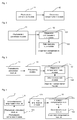
- this embodiment provides an optical receiver device, including a photoelectric conversion module 11 and a dispersion compensation module 12, wherein the photoelectric conversion module 11 is configured to receive an optical signal and to convert the optical signal into an electrical signal; and the dispersion compensation module 12 is configured to perform dispersion compensation on the electrical signal and to output the compensated electrical signal.
- the photoelectric conversion module 11 can be realized by a photoelectric converter; the dispersion compensation module 12 can be realized by a compensator. Both photoelectric converter and compensator can be realized by a light transceiver.
- the optical receiver device in this embodiment has a dispersion compensation function, which can reduce the channel chromatic dispersion cost of an optical signal, and prolong the transmission distance of the signal.
- the dispersion compensation module in this embodiment can replace a Limiting Amplifier (LA) in a conventional optical receiver device, enabling the optical receiver device to have a dispersion compensation function, and enabling cost reduction.
- the photoelectric conversion module 11 in this embodiment can be configured to receive a continuous-mode optical signal or a burst-mode optical signal, and convert the continuous-mode optical signal or burst-mode optical signal into an electrical signal.
- the optical receiver device in this embodiment can perform dispersion compensation on the received continuous-mode optical signal or burst-mode optical signal.
- the dispersion compensation module 12 in this embodiment might include an electronic dispersion compensation sub-module 121 and a data recovery sub-module 122, in which, the electronic dispersion compensation sub-module 121 is configured to perform dispersion compensation on the electrical signal; and the data recovery sub-module 122 is configured to perform phase retrieval and data shaping on the compensated electrical signal, and to output the compensated shaped electrical signal.
- both electronic dispersion compensation sub-module 121 and data recovery sub-module 122 can be realized by a Central Processing Unit (CPU), or a Digital Signal Processing (DSP) unit, or a Field-Programmable Gate Array (FPGA) and the like; all the CPU, DSP or FPGA can be embedded into a light transceiver.
- CPU Central Processing Unit
- DSP Digital Signal Processing
- FPGA Field-Programmable Gate Array
- the photoelectric conversion module 11 converts a received optical signal into an electrical signal and then transmits it to the dispersion compensation module 12, specifically to the electronic dispersion compensation sub-module 121; then, the electronic dispersion compensation sub-module 121 performs dispersion compensation on the received electrical signal, and transmits the compensated electrical signal to the data recovery sub-module 122; then, the data recovery sub-module 122 performs phase retrieval and data shaping on the compensated electrical signal, and outputs the compensated shaped electrical signal.
- the electronic dispersion compensation sub-module 121 can conduct dispersion compensation through a single or multiple tapped-delay-line feed-forward equalizer(s) or decision feedback equalizer(s). The feed-forward equalizer or the decision feedback equalizer performs adaptive dispersion compensation on the electrical signal.
- the optical receiver device in this embodiment further includes a processing module 13, which is configured to process the electrical signal according to the dispersion compensation requirement before the electronic dispersion compensation sub-module 121 performs dispersion compensation on the electrical signal, and to send the processed electrical signal to the dispersion compensation module 12, specifically, to the electronic dispersion compensation sub-module 121.
- processing module 13 processing the electrical signal according to the dispersion compensation requirement also can be understood as that: the processing module 13 processes the electrical signal so that the processed electrical signal can meet the requirement of dispersion compensation.
- the processing module 13 is a linear amplification module 131, which is configured to linearly amplify the voltage signal so that the signal meets the requirement of voltage range needed by dispersion compensation.
- the linear amplification module 131 also can be set in the photoelectrical conversion module 11, of course, the specific location can be decided as actually needed.
- the processing module 13 can be realized by an amplifier.
- the photoelectric conversion module 11 might include a photoelectric detection module 110 and a trans-impedance amplification module 111, in which, the photoelectric detection module 110 is configured to process a received optical signal and to convert it into a current signal, and the trans-impedance amplification module 111 is configured to perform trans-impedance conversion on the current signal to obtain a voltage signal; before performing dispersion compensation on the voltage signal, the linear amplification module 131 linearly amplifies the voltage signal so that the voltage signal meets the requirement of voltage range needed by dispersion compensation; the dispersion compensation module 12, specifically the electronic dispersion compensation sub-module 121 (for example, a feed-forward equalizer), performs dispersion compensation on the voltage signal meeting the requirement of voltage input range needed by dispersion compensation; the data recovery sub-module 122 performs phase retrieval and data shaping on the compensated voltage signal and finally outputs the compensated shaped signal.
- the photoelectric detection module 110 is configured to process a received optical signal and to convert it into a current signal
- the photoelectric detection module 110 might be a PIN photoelectric detection diode, or an Avalanche Photo Diode (APD); when the optical signal received by the photoelectric conversion module 11 is a burst-mode optical signal, the trans-impedance amplification module 111 in this embodiment might be a burst-mode trans-impedance amplifier; the data recovery sub-module 122 in this embodiment might be a fast data recovery sub-module, for adapting to process a burst-mode optical signal.
- APD Avalanche Photo Diode
- linear amplification module 131 configured to linearly amplify the voltage signal to enable the amplified signal to meet the requirement of voltage range needed by dispersion compensation also can be described as that:
- the optical receiver device in this embodiment further includes a signal detection module; as shown in Fig. 5 , the optical receiver device in this embodiment includes a photoelectric conversion module 11, a dispersion compensation module 12, a processing module 13 and a signal detection module 14, wherein the function and structure of the photoelectric conversion module 11 and the dispersion compensation module 12 can refer to the description in Embodiment 1; the signal detection module 14 in this embodiment is configured to detect the electrical signal output by the processing module 13, and to determine whether the signal received by the optical receiver device is lost.
- the photoelectric conversion module 11 in this embodiment converts the received optical signal into a voltage signal
- the processing module 13 is a linear amplification module 131
- the signal detection module 14 is a signal amplitude decision device 141
- the photoelectric conversion module 11 in this embodiment might include a photoelectric detection module 110 and a trans-impedance amplification module 111, wherein the photoelectric conversion module 11, specifically the photoelectric detection module 110, converts the received optical signal into a current signal, and the trans-impedance amplification module 111 converts the current signal into a voltage signal by trans-impedance conversion;
- the processing module 13, specifically the linear amplification module 131 linearly amplifies the voltage signal before performing dispersion compensation on the voltage signal, so that the voltage signal meets the requirement of voltage range needed by dispersion compensation;
- the signal detection module 14, specifically the signal amplitude decision device 141 is configured to detect the voltage value of the electrical signal output by the processing module 13, specifically the linear amplification module 131, and compare the voltage value
- the photoelectric conversion module 11 in this embodiment can receive a continuous-mode optical signal or a burst-mode optical signal, and converts the continuous-mode optical signal or burst-mode optical signal into a voltage signal.
- the optical receiver device in this embodiment can perform dispersion compensation on the received continuous-mode optical signal or burst-mode optical signal.
- the dispersion sub-module 121 might be a burst-mode feed-forward equalizer 121 a (or burst-mode feedback equalizer 121 b), the data recovery sub-module 122 is a fast clock recovery sub-module 122a; the burst-mode feed-forward equalizer 121 a (or burst-mode feedback equalizer 121 b) is configured to perform adaptive dispersion compensation on the voltage signal output by the linear amplification module 23; in Fig.
- the signal detection module 14, specifically the signal amplitude decision device 141 is configured to detect the voltage value of the electrical signal output by the linear amplification module 131, and compare the voltage value with a preset threshold, decide that the burst-mode optical signal received by the photoelectrical conversion module 11 is lost if the voltage value is lower than the preset threshold, and decide that the optical signal received is not lost if the voltage value is not lower than the preset threshold, that is, the photoelectric conversion module 11 receives signals normally; the signal amplitude decision device can notify the determination result to a subsequent system or module.
- the signal amplitude decision device 141 in this embodiment might be a fast signal amplitude decision device.
- the photoelectric detection module 110 might be a PIN photoelectric detection diode or an APD; when the optical signal received is a burst-mode optical signal, the trans-impedance amplification module 111 in this embodiment might be a burst-mode trans-impedance amplifier.
- the optical receiver device in this embodiment has a dispersion compensation function, which compensates the dispersion loss of a received optical signal (including in a burst mode and a continuous mode), reduces channel dispersion cost and prolongs the transmission distance of a subsequent modulated optical signal in an optical fibre, and meanwhile can determine whether the signal received by the device is lost, for the subsequent processing of signal.
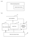
- this embodiment introduces an optical transceiving device, which includes the optical receiver devices described in Embodiment 1 and Embodiment 2; in this embodiment the optical transceiving device might be an optical transceiving integrated module; the structure of the optical transceiving device provided by this embodiment is described below in further detail.
- the optical transceiving device in this embodiment includes a light component 21, a dispersion compensation module 26, a laser driver 22, a micro controller 23 and an electrical interface module 24, wherein the light component 21, the dispersion compensation module 26 and the laser driver 22 compose an optical receiver device.
- the light component 21 is configured to perform photoelectric conversion, specifically, to convert a received optical signal into a voltage signal, and to convert an electrical data signal input by the electrical interface module 24 into an optical signal meeting requirements.
- the laser driver 22 is configured to convert a data signal input by the system via the electrical interface module 24 into a radio-frequency drive current, and then to drive the optical component 21 to convert the radio-frequency drive current into an optical signal meeting system standards.
- the micro controller 23 is configured to connect with the laser driver 22 and the electronic dispersion compensation module 12 via control signal lines or Inter-Integrated Circuit (IIC) buses, so as to monitor, collect and process related data, thereby enabling the output signal subjected to the optical-to-electrical conversion or electrical-to-optical conversion of the optical transceiving device provided by the embodiment of the disclosure to be stable, reliable and to meet system requirements.
- IIC Inter-Integrated Circuit
- the dispersion compensation module 26 is configured to perform dispersion compensation on an electrical signal output by the optical component.
- the electrical interface module 24 is configured to exchange an electrical signal between the optical receiver device and an external system.
- the optical component 21 includes the photoelectric conversion module 11 referred in Embodiment 1 and Embodiment 2; in this embodiment the function and structure of the dispersion compensation module 26 can refer to the introduction in the above embodiments.
- the optical transceiving device in this embodiment can convert an electrical signal needing transmitting into an optical signal and then transmit the optical signal out through an optical transmission network, or can receive an optical signal from the optical transmission network and convert the received optical signal into an electrical signal, and meanwhile perform dispersion compensation on the electrical signal, thereby reducing the channel dispersion cost of the optical signal and prolonging the transmission distance of the subsequent modulated optical signal.
- the light component shown in Fig. 10 might include a laser 211, a photoelectric detector 212 and a trans-impedance amplifier 213, wherein the laser 211 converts an electrical data signal to be transmitted into a standard optical signal under the driving of the laser driver; the photoelectric detector 212 converts the received optical signal into an optical current signal and the trans-impedance amplifier 213 converts the optical current signal into a differential analogue voltage signal.
- the linear amplification module 25 in Fig. 10 linearly amplifies or narrows the analogue voltage signal, so that the signal meets the requirement of voltage range needed by dispersion compensation.
- the dispersion compensation module 26 in Fig. 10 might include a feed-forward equalizer 261 (or feedback equalizer) and a Clock Data Recovery (CDR) sub-module 262; the feed-forward equalizer 261 (or a decision feedback equalizer) in the electronic dispersion compensation module 26 performs adaptive dispersion compensation on a signal output by the linear amplification module 25, and the CDR sub-module 262 performs phase retrieval and data shaping on the compensated signal, and finally outputs the compensated shaped signal to the electrical interface module.
- CDR Clock Data Recovery
- micro controller 23 in this embodiment also can be provided with an external IIC bus interface, which is connected with the IIC bus interface of a system board through the electrical interface module 24 of the optical receiver device, so that the system can diagnose and monitor the digital signal of the optical receiver device.
- the optical receiver device in this embodiment also might include a signal amplitude decision device 28, which is configured to judge the voltage signal output by the linear amplification module 26; the signal amplitude decision device 28 can preset a decision electrical level and judges the strength of a received signal; if the signal strength is higher than the decision electrical level, it is indicated that the received signal is normal, wherein RX LOS output is of low level or RX SD output is of high level; if the signal strength is lower than the decision electrical level, it is indicated that the received signal is lost, wherein RX LOS output is of high level or RX SD output is of low level; the signal decision is output to the system board through the electrical interface module 24.
- a signal amplitude decision device 28 can preset a decision electrical level and judges the strength of a received signal; if the signal strength is higher than the decision electrical level, it is indicated that the received signal is normal, wherein RX LOS output is of low level or RX SD output is of high level; if the signal strength is lower than the decision electrical level, it
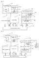
- the optical receiver device in this embodiment of the disclosure can be applied to various transceiving devices in optical communications; this embodiment introduces an Optical Network Unit (ONU) transceiving device, which as shown in Fig. 12 includes a single-fibre bidirectional device 31, a continuous-mode electronic dispersion compensator 32, a burst-mode laser driver 33, a micro controller 34, a signal amplitude decision device 35, a DC/DC booster circuit 36, an ONU electrical interface module 37 and a linear amplification module 38.
- ONU Optical Network Unit
- the single-fibre bidirectional device 31 includes a DML laser 311, an Avalanche Photo Diode (APD) 312 and a trans-impedance amplifier 313, wherein the DML laser 311 converts an electrical signal into an optical signal under the driving of the laser driver 33; the APD 312 and the trans-impedance amplifier 313 act together to convert a received optical signal into a voltage signal, the specific process please refer to the introduction of the same part in the above embodiments; the DC/DC booster circuit 36 supplies a bias voltage to the APD in the single-fibre bidirectional device 41; the linear amplification module 38 linearly amplifies the converted voltage signal for dispersion compensation; the continuous-mode electronic dispersion compensator 32 includes a feed-forward equalizer 321 (or a feedback equalizer) and a clock data recovery module, wherein the specific process can refer to that of the optical receiver device in the above embodiments; the signal amplitude decision device 35 can preset a decision electrical level and judges the strength of a received signal; if the
- the ONU transceiving device adopts a burst-mode laser driver 33 and a continuous-mode electronic dispersion compensator 32, which not only meets the photometric system indexes of ONU end but also supports an Optical Line Terminal (OLT) transceiving device to use a low-cost DML laser to replace an EML laser.
- OLT Optical Line Terminal
- the 10G EPON ONU optical transceiving device employing electronic dispersion compensation supports the 10G EPON OLT to adopt a 1577nm DML to transmit by 20km, which meets the standard requirements and effectively reduces the OLT's cost.
- the 10G EPON OLT optical module supporting an EML laser transmits a downlink signal by 60km, which effectively prolongs the transmission distance.
- This embodiment also provides an OLT transceiving device; as shown in Fig. 13 , the OLT transceiving device is similar to Fig. 12 and includes a single-fibre bidirectional device 41, a burst-mode electronic dispersion compensator 42, a continuous-mode laser driver 43, a micro controller 44, a fast signal amplitude decision device 45, a DC/DC booster circuit 46 and an OLT electrical interface module 47.
- the OLT transceiving device is similar to Fig. 12 and includes a single-fibre bidirectional device 41, a burst-mode electronic dispersion compensator 42, a continuous-mode laser driver 43, a micro controller 44, a fast signal amplitude decision device 45, a DC/DC booster circuit 46 and an OLT electrical interface module 47.
- the single-fibre bidirectional device 41 includes a DML laser 411, an APD 412 and a burst-mode trans-impedance amplifier 413, and a linear amplification module 48, wherein the DML laser 411 converts an electrical signal into an optical signal under the driving of the laser driver 43; the APD 412 and the burst-mode trans-impedance amplifier 413 act together to convert a received optical signal into a voltage signal, the specific process please refer to the introduction of the same part in the above embodiments; the linear amplification module 48 linearly amplifies the converted voltage signal for dispersion compensation; the DC/DC booster circuit 46 supplies a bias voltage to the APD in the single-fibre bidirectional device 41; the burst-mode electronic dispersion compensator 42 includes a burst-mode feed-forward equalizer 421 (or a burst-mode feedback equalizer) and a fast clock data recovery module 422 (BM CDR), wherein the two modules act together to implement the dispersion compensation function, the specific
- the OLT transceiving device in this embodiment adopts a continuous-mode laser driver and a burst-mode electronic dispersion compensator. It supports the wavelength switch of ONU, the uplink signal can adopt O band, C band or L band; besides the original O band, the ONU optical transceiving integrated module has a wider range of wavelengths to select. The ONU still can use a low-cost DML after wavelength is switched.
- this embodiment introduces an optical receiver method, which includes the following steps:
- the optical receiver method in this embodiment can perform dispersion compensation on an electrical signal converted from an optical signal when receiving the optical signal, to reduce the channel dispersion cost of the optical signal and prolong the transmission distance.
- Step 1001 performing dispersion compensation on the electrical signal includes:
- the method further includes:
- the method in this embodiment also can include:
- processing the electrical signal so that the signal meets the requirement of dispersion compensation includes:
- detecting the electrical signal meeting the dispersion compensation requirement and judging whether the received signal is lost include:
- Step 1001 the process of receiving an optical signal and converting the optical signal into an electrical signal includes:
Landscapes
- Physics & Mathematics (AREA)
- Engineering & Computer Science (AREA)
- Computer Networks & Wireless Communication (AREA)
- Signal Processing (AREA)
- Electromagnetism (AREA)
- Optics & Photonics (AREA)
- Optical Communication System (AREA)
Applications Claiming Priority (2)
| Application Number | Priority Date | Filing Date | Title |
|---|---|---|---|
| CN201310173544.3A CN104144018A (zh) | 2013-05-10 | 2013-05-10 | 光接收装置及方法、光收发一体模块 |
| PCT/CN2013/082118 WO2013189422A2 (fr) | 2013-05-10 | 2013-08-22 | Procédé et dispositif de réception de lumière, et module intégré d'émission-réception de lumière |
Publications (2)
| Publication Number | Publication Date |
|---|---|
| EP2996265A2 true EP2996265A2 (fr) | 2016-03-16 |
| EP2996265A4 EP2996265A4 (fr) | 2016-04-27 |
Family
ID=49769563
Family Applications (1)
| Application Number | Title | Priority Date | Filing Date |
|---|---|---|---|
| EP13806987.7A Withdrawn EP2996265A4 (fr) | 2013-05-10 | 2013-08-22 | Procédé et dispositif de réception de lumière, et module intégré d'émission-réception de lumière |
Country Status (4)
| Country | Link |
|---|---|
| US (1) | US20160099782A1 (fr) |
| EP (1) | EP2996265A4 (fr) |
| CN (1) | CN104144018A (fr) |
| WO (1) | WO2013189422A2 (fr) |
Cited By (1)
| Publication number | Priority date | Publication date | Assignee | Title |
|---|---|---|---|---|
| CN106330304A (zh) * | 2016-08-18 | 2017-01-11 | 青岛海信宽带多媒体技术有限公司 | 光模块的自动均衡方法及光模块 |
Families Citing this family (12)
| Publication number | Priority date | Publication date | Assignee | Title |
|---|---|---|---|---|
| JP2016536948A (ja) * | 2013-11-04 | 2016-11-24 | ゼットティーイー コーポレーションZte Corporation | 光通信における適応的予等化 |
| CN104467969B (zh) * | 2014-12-10 | 2017-03-22 | 北京理工大学 | 分数阶傅里叶变换测量光纤链路色散的方法 |
| CN105827321B (zh) * | 2015-01-05 | 2018-06-01 | 富士通株式会社 | 多载波光通信系统中的非线性补偿方法、装置和系统 |
| CN104967480B (zh) * | 2015-07-15 | 2016-12-07 | 北京理工大学 | 采用分数阶傅里叶变换监测光纤链路非线性效应的方法 |
| CN106572040B (zh) * | 2015-10-12 | 2020-04-21 | 富士通株式会社 | 发射端调制器的偏置漂移估计装置、补偿装置以及接收机 |
| FR3045992A1 (fr) * | 2015-12-18 | 2017-06-23 | Commissariat Energie Atomique | |
| CN105703824A (zh) * | 2016-04-29 | 2016-06-22 | 武汉光迅科技股份有限公司 | 一种高速光模块的接收测试装置及方法 |
| CN109302230B (zh) * | 2018-10-30 | 2020-09-08 | 新华三技术有限公司 | 一种光接口校准方法及装置 |
| CN115085804A (zh) * | 2021-03-11 | 2022-09-20 | 青岛海信宽带多媒体技术有限公司 | 一种光模块及接收光功率计算方法 |
| CN113206704B (zh) * | 2021-03-18 | 2022-11-15 | 武汉联特科技股份有限公司 | 一种带有edc功能且能实时校准接收信号的光模块及方法 |
| CN115021821B (zh) * | 2022-05-26 | 2023-05-12 | 厦门亿芯源半导体科技有限公司 | 基于xgspon搭配eml的10g速率olt端收发一体芯片 |
| CN120856233B (zh) * | 2025-09-25 | 2025-12-23 | 上海孛璞半导体技术有限公司 | 基于全链路参数优化的光互联仿真方法及系统 |
Family Cites Families (16)
| Publication number | Priority date | Publication date | Assignee | Title |
|---|---|---|---|---|
| JP2006287694A (ja) * | 2005-04-01 | 2006-10-19 | Sigma-Links Inc | 光通信システム及び光送信器 |
| US7427939B2 (en) * | 2006-12-28 | 2008-09-23 | Intel Corporation | Parallel processed electronic dispersion control |
| CN101039161B (zh) * | 2007-03-05 | 2011-10-26 | 华为技术有限公司 | 电光转换模块、光电转换模块 |
| JP2008244530A (ja) * | 2007-03-25 | 2008-10-09 | Nec Corp | 制御信号を用い波長分散を補償する光伝送装置及び方法 |
| WO2009054045A1 (fr) * | 2007-10-23 | 2009-04-30 | Fujitsu Limited | Compensateur de dispersion optique et récepteur optique |
| JP2009117921A (ja) * | 2007-11-01 | 2009-05-28 | Sumitomo Electric Ind Ltd | 光受信器、及び、光受信器の制御方法 |
| US8126338B2 (en) * | 2007-11-07 | 2012-02-28 | Discovery Semiconductors, Inc. | Method and apparatus for repeaterless high-speed optical transmission over single-mode fiber using coherent receiver and electronic dispersion compensation |
| JP5157536B2 (ja) * | 2008-03-06 | 2013-03-06 | 富士通株式会社 | トランバーサルフィルタのタップ係数制御装置及びタップ係数の制御方法、光受信装置並びに光通信システム |
| JP2010028340A (ja) * | 2008-07-17 | 2010-02-04 | Mitsubishi Electric Corp | 光受信器 |
| WO2012004890A1 (fr) * | 2010-07-09 | 2012-01-12 | 株式会社日立製作所 | Récepteur optique et système de transmission optique |
| JP5699583B2 (ja) * | 2010-12-17 | 2015-04-15 | 富士通株式会社 | 光受信機及び光受信方法 |
| US8594515B2 (en) * | 2011-03-03 | 2013-11-26 | Alcatel Lucent | Digital phase conjugation for fiber-optic links |
| EP2518914B1 (fr) * | 2011-08-01 | 2013-10-23 | Huawei Technologies Co. Ltd. | Dispositif récepteur cohérent et procédé de compensation de dispersion chromatique |
| US8593226B2 (en) * | 2011-09-07 | 2013-11-26 | International Business Machines Corporation | Transimpedance amplifier |
| US9112614B2 (en) * | 2012-03-02 | 2015-08-18 | Alcatel Lucent | Correction of a local-oscillator phase error in a coherent optical receiver |
| CN102917283B (zh) * | 2012-10-15 | 2015-09-30 | 青岛海信宽带多媒体技术有限公司 | 光网络单元以及光网络单元光模块 |
-
2013
- 2013-05-10 CN CN201310173544.3A patent/CN104144018A/zh active Pending
- 2013-08-22 WO PCT/CN2013/082118 patent/WO2013189422A2/fr not_active Ceased
- 2013-08-22 US US14/889,250 patent/US20160099782A1/en not_active Abandoned
- 2013-08-22 EP EP13806987.7A patent/EP2996265A4/fr not_active Withdrawn
Cited By (1)
| Publication number | Priority date | Publication date | Assignee | Title |
|---|---|---|---|---|
| CN106330304A (zh) * | 2016-08-18 | 2017-01-11 | 青岛海信宽带多媒体技术有限公司 | 光模块的自动均衡方法及光模块 |
Also Published As
| Publication number | Publication date |
|---|---|
| EP2996265A4 (fr) | 2016-04-27 |
| CN104144018A (zh) | 2014-11-12 |
| US20160099782A1 (en) | 2016-04-07 |
| WO2013189422A2 (fr) | 2013-12-27 |
| WO2013189422A3 (fr) | 2014-03-20 |
Similar Documents
| Publication | Publication Date | Title |
|---|---|---|
| EP2996265A2 (fr) | Procédé et dispositif de réception de lumière, et module intégré d'émission-réception de lumière | |
| CN102625199B (zh) | 双通道gepon olt csfp光模块 | |
| CN107517080B (zh) | 一种光功率检测方法、装置、设备及光模块 | |
| CN101848033B (zh) | 一种双速率接收装置 | |
| US20160248534A1 (en) | Method for processing optical signal, optical module and optical line terminal | |
| EP2833567B1 (fr) | Procédé de test de fibres optiques, appareil et système de réseau optique passif | |
| CN101895350A (zh) | 一种10g以太网无源网络单纤双向光模块 | |
| CN105703824A (zh) | 一种高速光模块的接收测试装置及方法 | |
| CN112311472B (zh) | 一种光模块接收装置、控制方法及存储介质 | |
| Omella et al. | 10 Gb/s RSOA transmission by direct duobinary modulation | |
| CN102104431A (zh) | 一种光收发模块中的双速率接收装置 | |
| US8571414B2 (en) | Optical transmission device, transmission and reception module, optical transmission system, and wavelength dispersion compensation method in optical transmission device | |
| CN102209281A (zh) | 10g epon olt单纤三向光模块 | |
| CN103281129A (zh) | 光模块及其电域色散补偿方法 | |
| CN105763245A (zh) | 一种光收发模块 | |
| CN104253651A (zh) | 一种基于光电光再生的万兆突发光放大器 | |
| CN106470075A (zh) | Olt光收发一体模块、处理多种pon的方法及系统 | |
| CN107579781B (zh) | 光信号接收模块及光信号收发装置 | |
| CN208424372U (zh) | 一种用于高速远距离传输的光收发一体组件 | |
| CN215378929U (zh) | 一种长距离光模块 | |
| CN101882958B (zh) | Apr保护方法及装置 | |
| CN201383812Y (zh) | 突发模式光发射机 | |
| CN106899352B (zh) | 一种基于qsfp28光模块的光电转换装置 | |
| EP4429129A1 (fr) | Procédés d'envoi et de réception de signaux d'enregistrement, dispositif d'émission optique, dispositif de réception optique, et système | |
| CN201937594U (zh) | Epon光线路终端用光模块 |
Legal Events
| Date | Code | Title | Description |
|---|---|---|---|
| PUAI | Public reference made under article 153(3) epc to a published international application that has entered the european phase |
Free format text: ORIGINAL CODE: 0009012 |
|
| 17P | Request for examination filed |
Effective date: 20151118 |
|
| AK | Designated contracting states |
Kind code of ref document: A2 Designated state(s): AL AT BE BG CH CY CZ DE DK EE ES FI FR GB GR HR HU IE IS IT LI LT LU LV MC MK MT NL NO PL PT RO RS SE SI SK SM TR |
|
| AX | Request for extension of the european patent |
Extension state: BA ME |
|
| A4 | Supplementary search report drawn up and despatched |
Effective date: 20160330 |
|
| RIC1 | Information provided on ipc code assigned before grant |
Ipc: H04B 10/61 20130101ALI20160322BHEP Ipc: H04B 10/2513 20130101AFI20160322BHEP Ipc: H04B 10/66 20130101ALI20160322BHEP |
|
| DAX | Request for extension of the european patent (deleted) | ||
| 17Q | First examination report despatched |
Effective date: 20180404 |
|
| STAA | Information on the status of an ep patent application or granted ep patent |
Free format text: STATUS: THE APPLICATION IS DEEMED TO BE WITHDRAWN |
|
| 18D | Application deemed to be withdrawn |
Effective date: 20180815 |