EP3000159B1 - Fehlerstromschutzschalter - Google Patents
Fehlerstromschutzschalter Download PDFInfo
- Publication number
- EP3000159B1 EP3000159B1 EP14725727.3A EP14725727A EP3000159B1 EP 3000159 B1 EP3000159 B1 EP 3000159B1 EP 14725727 A EP14725727 A EP 14725727A EP 3000159 B1 EP3000159 B1 EP 3000159B1
- Authority
- EP
- European Patent Office
- Prior art keywords
- mains voltage
- electronics
- residual current
- circuit breaker
- control
- Prior art date
- Legal status (The legal status is an assumption and is not a legal conclusion. Google has not performed a legal analysis and makes no representation as to the accuracy of the status listed.)
- Active
Links
Images
Classifications
-
- H—ELECTRICITY
- H01—ELECTRIC ELEMENTS
- H01H—ELECTRIC SWITCHES; RELAYS; SELECTORS; EMERGENCY PROTECTIVE DEVICES
- H01H47/00—Circuit arrangements not adapted to a particular application of the relay and designed to obtain desired operating characteristics or to provide energising current
- H01H47/007—Circuit arrangements not adapted to a particular application of the relay and designed to obtain desired operating characteristics or to provide energising current with galvanic isolation between controlling and controlled circuit, e.g. transformer relay
-
- H—ELECTRICITY
- H01—ELECTRIC ELEMENTS
- H01H—ELECTRIC SWITCHES; RELAYS; SELECTORS; EMERGENCY PROTECTIVE DEVICES
- H01H83/00—Protective switches, e.g. circuit-breaking switches, or protective relays operated by abnormal electrical conditions otherwise than solely by excess current
- H01H83/02—Protective switches, e.g. circuit-breaking switches, or protective relays operated by abnormal electrical conditions otherwise than solely by excess current operated by earth fault currents
-
- H—ELECTRICITY
- H02—GENERATION; CONVERSION OR DISTRIBUTION OF ELECTRIC POWER
- H02H—EMERGENCY PROTECTIVE CIRCUIT ARRANGEMENTS
- H02H3/00—Emergency protective circuit arrangements for automatic disconnection directly responsive to an undesired change from normal electric working condition with or without subsequent reconnection ; integrated protection
- H02H3/02—Details
- H02H3/04—Details with warning or supervision in addition to disconnection, e.g. for indicating that protective apparatus has functioned
- H02H3/044—Checking correct functioning of protective arrangements, e.g. by simulating a fault
-
- H—ELECTRICITY
- H02—GENERATION; CONVERSION OR DISTRIBUTION OF ELECTRIC POWER
- H02H—EMERGENCY PROTECTIVE CIRCUIT ARRANGEMENTS
- H02H3/00—Emergency protective circuit arrangements for automatic disconnection directly responsive to an undesired change from normal electric working condition with or without subsequent reconnection ; integrated protection
- H02H3/02—Details
- H02H3/05—Details with means for increasing reliability, e.g. redundancy arrangements
-
- H—ELECTRICITY
- H02—GENERATION; CONVERSION OR DISTRIBUTION OF ELECTRIC POWER
- H02H—EMERGENCY PROTECTIVE CIRCUIT ARRANGEMENTS
- H02H3/00—Emergency protective circuit arrangements for automatic disconnection directly responsive to an undesired change from normal electric working condition with or without subsequent reconnection ; integrated protection
- H02H3/26—Emergency protective circuit arrangements for automatic disconnection directly responsive to an undesired change from normal electric working condition with or without subsequent reconnection ; integrated protection responsive to difference between voltages or between currents; responsive to phase angle between voltages or between currents
- H02H3/32—Emergency protective circuit arrangements for automatic disconnection directly responsive to an undesired change from normal electric working condition with or without subsequent reconnection ; integrated protection responsive to difference between voltages or between currents; responsive to phase angle between voltages or between currents involving comparison of the voltage or current values at corresponding points in different conductors of a single system, e.g. of currents in go and return conductors
- H02H3/33—Emergency protective circuit arrangements for automatic disconnection directly responsive to an undesired change from normal electric working condition with or without subsequent reconnection ; integrated protection responsive to difference between voltages or between currents; responsive to phase angle between voltages or between currents involving comparison of the voltage or current values at corresponding points in different conductors of a single system, e.g. of currents in go and return conductors using summation current transformers
-
- H—ELECTRICITY
- H02—GENERATION; CONVERSION OR DISTRIBUTION OF ELECTRIC POWER
- H02H—EMERGENCY PROTECTIVE CIRCUIT ARRANGEMENTS
- H02H3/00—Emergency protective circuit arrangements for automatic disconnection directly responsive to an undesired change from normal electric working condition with or without subsequent reconnection ; integrated protection
- H02H3/26—Emergency protective circuit arrangements for automatic disconnection directly responsive to an undesired change from normal electric working condition with or without subsequent reconnection ; integrated protection responsive to difference between voltages or between currents; responsive to phase angle between voltages or between currents
- H02H3/32—Emergency protective circuit arrangements for automatic disconnection directly responsive to an undesired change from normal electric working condition with or without subsequent reconnection ; integrated protection responsive to difference between voltages or between currents; responsive to phase angle between voltages or between currents involving comparison of the voltage or current values at corresponding points in different conductors of a single system, e.g. of currents in go and return conductors
- H02H3/33—Emergency protective circuit arrangements for automatic disconnection directly responsive to an undesired change from normal electric working condition with or without subsequent reconnection ; integrated protection responsive to difference between voltages or between currents; responsive to phase angle between voltages or between currents involving comparison of the voltage or current values at corresponding points in different conductors of a single system, e.g. of currents in go and return conductors using summation current transformers
- H02H3/332—Emergency protective circuit arrangements for automatic disconnection directly responsive to an undesired change from normal electric working condition with or without subsequent reconnection ; integrated protection responsive to difference between voltages or between currents; responsive to phase angle between voltages or between currents involving comparison of the voltage or current values at corresponding points in different conductors of a single system, e.g. of currents in go and return conductors using summation current transformers with means responsive to DC component in the fault current
-
- H—ELECTRICITY
- H01—ELECTRIC ELEMENTS
- H01H—ELECTRIC SWITCHES; RELAYS; SELECTORS; EMERGENCY PROTECTIVE DEVICES
- H01H83/00—Protective switches, e.g. circuit-breaking switches, or protective relays operated by abnormal electrical conditions otherwise than solely by excess current
- H01H83/14—Protective switches, e.g. circuit-breaking switches, or protective relays operated by abnormal electrical conditions otherwise than solely by excess current operated by imbalance of two or more currents or voltages, e.g. for differential protection
- H01H83/144—Protective switches, e.g. circuit-breaking switches, or protective relays operated by abnormal electrical conditions otherwise than solely by excess current operated by imbalance of two or more currents or voltages, e.g. for differential protection with differential transformer
Definitions
- the invention relates to a residual current circuit breaker according to the preamble of claim 1.
- a residual current circuit breaker In many countries, it is required by law that a residual current circuit breaker must have the ability to detect and, if necessary, trigger a sinusoidal fault current completely independently of the mains voltage. However, such residual current circuit breakers have only a very limited functionality. Additional requirements for a residual current circuit breaker, such as the safe detection of smooth and / or pulsating DC residual currents, usually require a mains voltage-dependent triggering circuit for their implementation. However, it must be ensured that, in the event of a failure of this mains-voltage-dependent tripping circuit, the required basic functions continue to be fulfilled by the relevant residual current circuit breaker.
- the DE 197 35 412 A1 describes a residual current device with two trip circuits, wherein one of the trigger circuits for AC and pulse fault currents is formed, and the other DC residual current trip circuit.
- EP 1 478 069 A1 describes a universal current-sensitive residual current device with a mains voltage-independent sensor device for AC residual current and a mains voltage-dependent sensor device for smooth DC residual current, AC residual current and pulsating DC residual current.
- the object of the invention is therefore to provide a residual current circuit breaker of the type mentioned, with which the mentioned disadvantages can be avoided, and in which it can be ensured that is switched to a fault in the mains voltage-dependent tripping circuit on the mains voltage independent trigger circuit.
- the mains-voltage-dependent triggering circuit is only operated as long as it also functions properly or as intended.
- the control electronics off the mains voltage-dependent tripping electronics or electrically separated from the corresponding winding of the summation current transformer, and at the same time activates the mains voltage-independent tripping electronics by these connected in circuit technology with the corresponding winding of the summation current transformer or contacted.
- This not only ensures that one of the two tripping electronics is always active, but rather that the mains voltage-dependent tripping electronics are only in operation if they also function according to their specifications.
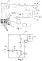
- Fig. 1 shows a block diagram of a residual current circuit breaker 1 with a summation current transformer 2, which primary windings 3 and a secondary winding 4 and a tertiary winding 6, wherein the secondary winding 4 is connected in circuit technology with a mains voltage independent tripping electronics 5, wherein the tertiary winding 6 is connected in circuit technology with a mains voltage-dependent tripping electronics 7, wherein the residual current circuit breaker 1 a Control electronics 21 which is designed to control a switch 8 at specifiable control by the mains voltage-dependent tripping electronics 7, and that the switch 8 interrupts the contact of the secondary winding 4 to the mains voltage-independent tripping electronics 5 and, in particular substantially simultaneously, the contact of the Tertiärwicklung 6 to the mains voltage-dependent tripping electronics 7 manufactures.
- the mains voltage-dependent triggering circuit 7 is only operated as long as it also functions properly or as intended.
- this no longer controls the control electronics 21 in the expected form of this, whereupon the control electronics 21, the mains voltage-dependent tripping electronics 7 turns off or electrically separated from the corresponding tertiary winding 6 of the summation current transformer 2, and at the same time the mains voltage-independent tripping electronics 5 is activated by being connected or contacted by circuitry with the corresponding secondary winding 4 of the summation current transformer 2.
- This not only ensures that one of the two tripping electronics 5, 7 is always active, but rather that the mains voltage-dependent tripping electronics 7 is only in operation, if this also works according to their specifications.
- the subject residual current circuit breaker 1 has a summation current transformer 2, which has a core, in particular a toroidal core. This core has an opening through which the primary windings 3 are guided.
- the term primary winding 3 also includes that the relevant conductors, each of which opens into connection terminals of the residual current circuit breaker 1, are only passed through the opening, without embracing the cross section of the core. It is envisaged to connect to the respective terminals of the residual current circuit breaker 1, the power line N, L 1 , L 2 , L 3 , wherein two-pole versions of the subject residual current circuit breaker 1 may be provided.
- a secondary winding 4 and a tertiary winding 6 are further arranged, which are typically around the cross section of the Kerns are wound.
- the subject residual current circuit breaker 1 has a mains voltage-independent tripping electronics 5 and a mains voltage-dependent tripping electronics 7.
- the mains voltage-independent tripping electronics 5 is circuitally connected or contacted with the secondary winding 4, and can be carried out according to the known embodiments of corresponding mains voltage-independent tripping electronics 5, wherein in particular the training selbiger comprising an energy storage circuit and a downstream of this comparator circuit is provided.
- the mains voltage-dependent tripping electronics 7 is preferred Fig. 1 formed, and connected to the tertiary winding 6 circuitry or contacted.
- the mains voltage-dependent tripping electronics 5 has a digital signal processing unit 11, which is preferably designed as a microcomputer or microcontroller.
- the mains voltage-dependent tripping electronics 7 is also designed for the detection of smooth DC residual currents.
- the illustrated preferred embodiment of the mains voltage-dependent tripping electronics 7 will be described below.
- the digital signal processing unit 11 controls a sinusoidal current source 14, which is connected in terms of circuitry to the tertiary winding 6. This makes it possible to pre-magnetize the core of the summation current transformer 2 with an exciter frequency f.
- a DC residual current occurs due to non-linear processes, signal components occur at twice the exciter frequency 2f, which are proportional to the magnitude of the DC residual current that occurs.
- the tertiary winding 6 is further connected in terms of circuitry to a signal detection unit 15, which receives the occurring signals of the tertiary winding 6 and optionally processed and passed on to the digital signal processing unit 11. It can be provided that the Signal detection unit 15 is formed in particular for detecting the occurring at the double excitation frequency 2f signal components.
- the incoming, and provided by the signal detection unit 15 error current signals are processed and thereby compared with stored limits or Auslinate biblical.
- the digital signal processing unit preferably generates a signal for predefinable activation of the control electronics 21. It is provided that the corresponding signal is a specifiable changing control signal, in particular a predeterminable and periodically alternating signal, in particular a rectangular signal. In this case, provision is made in particular to implement the generation of the relevant signal in the digital signal processing unit 11 in such a way that a disruption of the internal program sequence in the digital signal processing unit 11 also leads to a disruption of the generation of the relevant signal.
- the digital signal processing unit 11 therefore controls the control electronics 21 with the relevant signal in trouble-free operation. It is provided that the control electronics 21 in the appropriate control by the mains voltage-dependent tripping electronics 7, a switch 8, which is arranged in the residual current circuit breaker 1 between the secondary winding 4 and tertiary winding 6 and the respective associated tripping electronics 5, 7, controls. It is further provided that the switch 8 interrupts the contact of the secondary winding 4 to the mains voltage-independent tripping electronics 5 in the activated state and the contact of the tertiary winding 6 to the mains voltage-dependent tripping electronics 7 produces.
- the switch 8 is preferably designed as a semiconductor relay 9, wherein in particular it is provided that the switch is designed as a photo-MOS relay 10. Due to the design as a semiconductor relay 9, a short switching time can be achieved, as well as a safe long-term operation. Due to the preferred embodiment of the same as a photo-MOS relay 10 also a galvanic isolation of the individual circuits can be achieved, whereby the proper operation of the different circuits of the residual current circuit breaker 1 advantageous is supported.
- the switch 8 has according to the preferred embodiment, two switching paths, which are coupled so that each time the switch 8 both switching sections are switched.
- a first switching contact 16 which is arranged in the circuit connection between the tertiary winding 6 and the mains voltage-dependent tripping electronics 7, designed as a so-called.
- Normally open and a second switching contact 17, which in the circuit connection between the secondary winding 4 and the mains voltage independent tripping electronics. 5 is arranged, designed as a so-called. Opener.
- the term "normally open” means that the relevant switch 8 closes or closes the relevant switching contact 16 when it is actuated and only during such activation, and if no corresponding activation takes place, the relevant switching contact 16 is not closed, and therefore none conductive connection via this switching contact 16 is. According to the preferred embodiment, it is provided that the switch is driven by a high-time signal lasting for a long time.
- the residual current circuit breaker 1 further has a power supply unit 12 for supplying the mains voltage-dependent components.
- Fig. 2 illustrated preferred embodiment of an electronic control unit 21 described.
- the digital signal processing unit 11 is preferably designed to output a specifiable changing control signal to a control input 23 of the control electronics 21.
- the digital signal processing unit 11 comprises a processor which performs the signal analysis of the error current signal and optionally comprises an analog / digital converter
- the digital signal processing unit 11 additionally generates and outputs the prescribable changing control signal is that this specifiable changing control signal is generated only when the digital signal processing unit 11 is working properly specifiable. This can be easily achieved by programming the processor accordingly.
- a corresponding control electronics 21 is provided according to the preferred embodiment, which only activates an output when applied to the control input 23, the corresponding predetermined control signal.
- any type of corresponding circuit arrangement can be provided.
- Fig. 2 shows a particularly preferred embodiment of an electronic control unit 21 for a periodically rectangular control signal, wherein in the representation of the internationally accepted switching symbols and dimensions were used.
- the output of the control electronics 21 is connected to the input of the semiconductor relay 9, which according to Fig. 2 is designed as a photo-MOS relay 10, wherein in Fig. 2 only the LEDs provided for driving are shown, therefore not the complete photo-MOS relay 10th
- the subject residual current circuit breaker also has a tripping relay 13, which is connected by means of the diodes 19, 20 with the two tripping electronics 5, 7 circuit technology.
Landscapes
- Engineering & Computer Science (AREA)
- Power Engineering (AREA)
- Driving Mechanisms And Operating Circuits Of Arc-Extinguishing High-Tension Switches (AREA)
- Emergency Protection Circuit Devices (AREA)
Description
- Die Erfindung betrifft einen Fehlerstromschutzschalter gemäß dem Oberbegriff des Patentanspruches 1.
- In zahlreichen Ländern ist gesetzlich vorgeschrieben, dass ein Fehlerstromschutzschalter die Fähigkeit aufweisen muss vollkommen netzspannungsunabhängig einen sinusförmigen Fehlerstrom zu detektieren und gegebenenfalls auszulösen. Allerdings weisen derartige Fehlerstromschutzschalter nur eine sehr eingeschränkte Funktionalität auf. Zusätzliche Anforderungen an einen Fehlerstromschutzschalter, wie etwa das sichere Detektieren glatter und/oder pulsierender Gleichfehlerströme, erfordern in der Regel zu deren Umsetzung eine netzspannungsabhängige Auslöseschaltung. Dabei ist allerdings sicherzustellen, dass bei einem Ausfall dieser netzspannungsabhängigen Auslöseschaltung weiterhin die geforderten Grundfunktionen weiterhin durch den betreffenden Fehlerstromschutzschalter erfüllt werden.
- Es sind daher Fehlerstromschutzschalter bekannt, welche sowohl eine netzspannungsunabhängige Auslöseschaltung als auch eine netzspannungsabhängige Auslöseschaltung aufweisen. Es hat sich allerdings als problematisch herausgestellt bei derartigen Fehlerstromschutzschaltern sicherzustellen, dass die netzspannungsabhängige Auslöseschaltung auch tatsächlich nur bei einer ordnungsgemäßen Funktion derselben in Betrieb ist und ansonsten die netzspannungsunabhängige Auslöseschaltung Verwendung findet.
- Die
DE 197 35 412 A1 beschreibt eine Fehlerstromschutzeinrichtung mit zwei Auslöseschaltungen, wobei eine der Auslöseschaltungen für Wechsel-und Pulsfehlerströme ausgebildet ist, und die andere Auslöseschaltung für Gleichfehlerstrom. - Aus der
EP 1 478 069 A1 beschreibt eine allstromsensitive Fehlerstromschutzeinrichtung mit einer netzspannungsunabhängigen Sensoreinrichtung für Wechselfehlerstrom und einer netzspannungsabhängigen Sensoreinrichtung für glatten Gleichfehlerstrom, Wechselfehlerstrom und pulsierenden Gleichfehlerstrom. - Aufgabe der Erfindung ist es daher einen Fehlerstromschutzschalter der eingangs genannten Art anzugeben, mit welchem die genannten Nachteile vermieden werden können, und bei welchem sichergestellt werden kann, dass bei einem Fehler in der netzspannungsabhängigen Auslöseschaltung auf die netzspannungsunabhängige Auslöseschaltung gewechselt wird.
- Erfindungsgemäß wird dies durch die Merkmale des Patentanspruches 1 erreicht.
- Dadurch kann sichergestellt werden, dass die netzspannungsabhängige Auslöseschaltung nur betrieben wird solange diese auch ordnungsgemäß bzw. wie vorgesehen funktioniert. Bereits bei einer Störung der Funktion der Auslöseelektronik steuert diese nicht mehr ordnungsgemäß die Steuerelektronik in der von dieser erwarteten Form an, woraufhin die Steuerelektronik die netzspannungsabhängige Auslöseelektronik abschaltet bzw. von der entsprechenden Wicklung des Summenstromwandlers elektrisch trennt, und gleichzeitig die netzspannungsunabhängige Auslöseelektronik aktiviert, indem diese mit der entsprechenden Wicklung des Summenstromwandlers schaltungstechnisch verbunden bzw. kontaktiert wird. Dadurch kann nicht nur sichergestellt werden, dass stets eine der beiden Auslöseelektroniken aktiv ist, sondern vielmehr, dass die netzspannungsabhängige Auslöseelektronik nur in Betrieb ist, wenn diese auch entsprechend deren Vorgaben funktioniert.
- Die Unteransprüche betreffen weitere vorteilhafte Ausgestaltungen der Erfindung.
- Ausdrücklich wird hiermit auf den Wortlaut der Patentansprüche Bezug genommen, wodurch die Ansprüche an dieser Stelle durch Bezugnahme in die Beschreibung eingefügt sind und als wörtlich wiedergegeben gelten.
- Die Erfindung wird unter Bezugnahme auf die beigeschlossenen Zeichnungen, in welchen eine lediglich bevorzugte Ausführungsform beispielhaft dargestellt ist, näher beschrieben. Dabei zeigt:
-
Fig. 1 ein Blockschaltbild der bevorzugten Ausführungsform eines Fehlerstromschutzschalters; und -
Fig. 2 eine bevorzugte Ausführungsform einer Steuerelektronik eines Fehlerstromschutzschalters gemäßFig. 1 . -
Fig. 1 zeigt ein Blockschaltbild eines Fehlerstromschutzschalters 1 mit einem Summenstromwandler 2, welcher Primärwicklungen 3 sowie eine Sekundärwicklung 4 und eine Tertiärwicklung 6 aufweist, wobei die Sekundärwicklung 4 mit einer netzspannungsunabhängigen Auslöseelektronik 5 schaltungstechnisch verbunden ist, wobei die Tertiärwicklung 6 mit einer netzspannungsabhängigen Auslöseelektronik 7 schaltungstechnisch verbunden ist, wobei der Fehlerstromschutzschalter 1 eine Steuerelektronik 21 aufweist, welche dazu ausgebildet ist, bei vorgebbarer Ansteuerung durch die netzspannungsabhängige Auslöseelektronik 7 einen Schalter 8 anzusteuern, und dass der Schalter 8 im angesteuerten Zustand den Kontakt der Sekundärwicklung 4 zur netzspannungsunabhängigen Auslöseelektronik 5 unterbricht und, insbesondere im Wesentlichen gleichzeitig, den Kontakt der Tertiärwicklung 6 zur netzspannungsabhängigen Auslöseelektronik 7 herstellt. - Dadurch kann sichergestellt werden, dass die netzspannungsabhängige Auslöseschaltung 7 nur betrieben wird solange diese auch ordnungsgemäß bzw. wie vorgesehen funktioniert. Bereits bei einer Störung der Funktion der netzspannungsabhängigen Auslöseelektronik 7 steuert diese nicht mehr ordnungsgemäß die Steuerelektronik 21 in der von dieser erwarteten Form an, woraufhin die Steuerelektronik 21 die netzspannungsabhängige Auslöseelektronik 7 abschaltet bzw. von der entsprechenden Tertiärwicklung 6 des Summenstromwandlers 2 elektrisch trennt, und gleichzeitig die netzspannungsunabhängige Auslöseelektronik 5 aktiviert, indem diese mit der entsprechenden Sekundärwicklung 4 des Summenstromwandlers 2 schaltungstechnisch verbunden bzw. kontaktiert wird. Dadurch kann nicht nur sichergestellt werden, dass stets eine der beiden Auslöseelektroniken 5, 7 aktiv ist, sondern vielmehr, dass die netzspannungsabhängige Auslöseelektronik 7 nur in Betrieb ist, wenn diese auch entsprechend deren Vorgaben funktioniert.
- Der gegenständliche Fehlerstromschutzschalter 1 weist einen Summenstromwandler 2 auf, welcher einen Kern aufweist, insbesondere einen Ringbandkern. Dieser Kern weist eine Öffnung auf, durch welche die Primärwicklungen 3 geführt sind. Die Bezeichnung Primärwicklung 3 schließ dabei auch ein, dass die betreffenden Leiter, die jeweils in Anschlussklemmen des Fehlerstromschutzschalters 1 münden, lediglich durch die Öffnung hindurchgeführt sind, ohne den Querschnitt des Kerns zu umfassen. Es ist vorgesehen an die betreffenden Anschlussklemmen des Fehlerstromschutzschalters 1 die Netzleiter N, L1, L2, L3 anzuschließen, wobei auch zweipolige Ausführungen des gegenständlichen Fehlerstromschutzschalters 1 vorgesehen sein können.
- Auf dem Summenstromwandler 2 sind weiters eine Sekundärwicklung 4 und eine Tertiärwicklung 6 angeordnet, welche dabei typischerweise um den Querschnitt des Kerns gewickelt sind.
- Der gegenständliche Fehlerstromschutzschalter 1 weist eine netzspannungsunabhängige Auslöseelektronik 5 sowie eine netzspannungsabhängigen Auslöseelektronik 7 auf.
- Die netzspannungsunabhängige Auslöseelektronik 5 ist schaltungstechnisch mit der Sekundärwicklung 4 verbunden bzw. kontaktiert, und kann entsprechend den bekannten Ausführungsformen entsprechender netzspannungsunabhängiger Auslöseelektroniken 5 ausgeführt sind, wobei insbesondere die Ausbildung selbiger umfassend eine Energiespeicherschaltung sowie eine dieser nachgeschaltete Komparatorschaltung vorgesehen ist.
- Die netzspannungsabhängige Auslöseelektronik 7 ist bevorzugt zufolge
Fig. 1 ausgebildet, und mit der Tertiärwicklung 6 schaltungstechnisch verbunden bzw. kontaktiert. Die netzspannungsabhängige Auslöseelektronik 5 weist eine digitale Signalverarbeitungseinheit 11 auf, welche bevorzugt als Mikrocomputer bzw. Mikrocontroller ausgebildet ist. - Gemäß der bevorzugten Ausführungsform ist vorgesehen, dass die netzspannungsabhängige Auslöseelektronik 7 auch zur Detektion glatter Gleichfehlerströme ausgebildet ist. Nachfolgend wird die dargestellte bevorzugte Ausführungsform der netzspannungsabhängigen Auslöseelektronik 7 beschrieben.
- Die digitale Signalverarbeitungseinheit 11 steuert dabei eine Sinusstromquelle14 an, welche schaltungstechnisch mit der Tertiärwicklung 6 verbunden ist. Dadurch besteht die Möglichkeit den Kern des Summenstromwandlers 2 mit einer Erregerfrequenz f vorzumagnetisieren. Beim Auftreten eines Gleichfehlerstromes kommt es aufgrund nichtlinearer Vorgänge zum Auftreten von Signalkomponenten bei der doppelten Erregerfrequenz 2f, welche proportional der Höhe des auftretenden Gleichfehlerstromes sind.
- Die Tertiärwicklung 6 ist weiters schaltungstechnisch mit einer Signalerfassungseinheit 15 verbunden, welche die auftretenden Signale der Tertiärwicklung 6 aufnimmt und gegebenenfalls aufbereitet und an die digitale Signalverarbeitungseinheit 11 weitergibt. Es kann dabei vorgesehen sein, dass die Signalerfassungseinheit 15 insbesondere auch zur Detektion der bei der doppelten Erregerfrequenz 2f auftretenden Signalkomponenten ausgebildet ist.
- In der digitalen Signalverarbeitungseinheit 11 werden die eingehenden, und durch die Signalerfassungseinheit 15 bereitgestellten, Fehlerstromsignale verarbeitet und dabei mit gespeicherten Grenzwerten bzw. Auslösebedingungen verglichen.
- Zudem Erzeugt die digitale Signalverarbeitungseinheit bevorzugt ein Signal zur vorgebbaren Ansteuerung der Steuerelektronik 21. Dabei ist vorgesehen, dass es sich bei dem entsprechenden Signal um ein vorgebbar änderndes Steuersignal handelt, insbesondere um ein vorgebbar und periodisch alternierendes Signal, insbesondere um ein Rechtecksignal. Es ist dabei insbesondere vorgesehen die Erzeugung des betreffenden Signals derart in die digitale Signalverarbeitungseinheit 11 zu implementieren, dass eine Störung des internen Programmablaufes in der digitale Signalverarbeitungseinheit 11 auch zu einer Störung der Erzeugung des betreffenden Signals führt.
- Die digitale Signalverarbeitungseinheit 11 steuert daher bei störungsfreiem Betrieb die Steuerelektronik 21 mit dem betreffenden Signal an. Es ist dabei vorgesehen, dass die Steuerelektronik 21 bei der entsprechenden Ansteuerung durch die netzspannungsabhängige Auslöseelektronik 7 einen Schalter 8, welcher in dem Fehlerstromschutzschalter 1 zwischen Sekundärwicklung 4 bzw. Tertiärwicklung 6 und den jeweils zugehörigen Auslöseelektroniken 5, 7 angeordnet ist, ansteuert. Dabei ist weiters vorgesehen, dass der Schalter 8 im angesteuerten Zustand den Kontakt der Sekundärwicklung 4 zur netzspannungsunabhängigen Auslöseelektronik 5 unterbricht und den Kontakt der Tertiärwicklung 6 zur netzspannungsabhängigen Auslöseelektronik 7 herstellt.
- Der Schalter 8 ist dabei bevorzugt als Halbleiterrelais 9 ausgebildet, wobei insbesondere vorgesehen ist, dass der Schalter als Photo-MOS-Relais 10 ausgebildet ist. Durch die Ausbildung als Halbleiterrelais 9 kann eine kurze Schaltzeit erzielt werden, sowie ein sicherer Langzeitbetrieb. Durch die bevorzugte Ausbildung desselben als Photo-MOS-Relais 10 kann zudem eine galvanische Trennung der einzelnen Schaltkreise erzielt werden, wodurch die ordnungsgemäße Funktion der unterschiedlichen Schaltkreise des Fehlerstromschutzschalters 1 vorteilhaft unterstützt wird.
- Der Schalter 8 weist gemäß der bevorzugten Ausführungsform zwei Schaltstrecken auf, welche gekoppelt sind, sodass bei jeder Betätigung des Schalters 8 jeweils beide Schalstrecken geschaltet werden. Dabei ist ein erster Schaltkontakt 16, welcher in der schaltungstechnischen Verbindung zwischen der Tertiärwicklung 6 und der netzspannungsabhängigen Auslöseelektronik 7 angeordnet ist, als sog. Schließer ausgebildet, und ein zweiter Schaltkontakt 17, welcher in der schaltungstechnischen Verbindung zwischen der Sekundärwicklung 4 und der netzspannungsunabhängigen Auslöseelektronik 5 angeordnet ist, als sog. Öffner ausgebildet. Der Begriff "Schließer" bedeutet dabei, dass der betreffende Schalter 8 bei einer Ansteuerung und nur während einer solchen Ansteuerung den betreffenden Schaltkontakt 16 schließt bzw. geschlossen hält, und sofern keine entsprechende Ansteuerung erfolgt, der betreffende Schaltkontakt 16 nicht geschlossen ist, und daher keine leitende Verbindung über diesen Schaltkontakt 16 besteht. Gemäß der bevorzugten Ausführungsform ist vorgesehen, dass der Schalter durch ein zeitlich andauerndes High-Signal angesteuert wird.
- Der Fehlerstromschutzschalter 1 weist weiters ein Netzteil 12 auf, zur Versorgung der netzspannungsabhängigen Komponenten.
- Nachfolgend wird eine in
Fig. 2 dargestellte bevorzugte Ausführungsform einer Steuerelektronik 21 beschrieben. - Wie bereits dargelegt ist die digitale Signalverarbeitungseinheit 11 bevorzugt zur Ausgabe eines sich vorgebbar ändernden Steuersignals an einen Steuereingang 23 der Steuerelektronik 21 ausgebildet. Gemäß der bevorzugten Ausführungsform, dergemäß die digitale Signalverarbeitungseinheit 11 einen Prozessor aufweist, welcher die Signalanalyse des Fehlerstromsignals durchführt, und hiezu gegebenenfalls einen Analog/Digitalwandler umfasst, ist vorgesehen, dass die digitale Signalverarbeitungseinheit 11 zusätzlich das sich vorgebbar ändernde Steuersignal erzeugt und ausgibt, wobei vorgesehen ist, dass dieses sich vorgebbar ändernde Steuersignal nur dann erzeugt wird, wenn die digitale Signalverarbeitungseinheit 11 ordnungsgemäß vorgebbar arbeitet. Dies kann durch entsprechende Programmierung des Prozessors einfach erreicht werden. Bevorzugt ist hiebei vorgesehen, dass - zusätzlich zu den anderen Arbeitsroutinen - weiters etwa ein vorgebbar periodisches Rechtecksignal als Steuersignal an den Steuereingang 23 der Steuerelektronik 21 ausgegeben wird, wie dies auch in
Fig. 2 dargestellt ist. Es können aber auch andere Arten eines Steuersignals generiert und ausgegeben werden. Dadurch wird erreicht, dass bei einem Fehlerstromschutzschalter 1 mit netzspannungsabhängiger Auslöseelektronik 7 nicht nur das Vorhandensein der Versorgungsspannung oder der Bauteile überprüft wird, sondern tatsächlich die korrekte bzw. vorgegebene Funktion der für die netzspannungsabhängige Auslösung notwendigen Baugruppen. Dadurch kann sichergestellt werden, dass ein derartiger Fehlerstromschutzschalter 1 bei einer nicht funktionierenden netzspannungsabhängigen Auslöseelektronik 7 als voll netzspannungsunabhängiger Fehlerstromschutzschalter 1 weiterarbeitet. Dadurch werden auch die Normen voll erfüllt, welche netzspannungsabhängige Fehlerstromschutzschalter 1 nicht zulassen. - Für die entsprechende Funktion des Schalters 8 ist gemäß der bevorzugten Ausführungsform eine entsprechende Steuerelektronik 21 vorgesehen, welche einen Ausgang lediglich dann aktiviert, wenn an deren Steuereingang 23 das entsprechend vorgegebene Steuersignal anliegt. Grundsätzlich kann dabei jede Art einer entsprechenden Schaltungsanordnung vorgesehen sein.
-
Fig. 2 zeigt eine besonders bevorzugte Ausbildung einer Steuerelektronik 21 für ein periodisch rechteckförmiges Steuersignal, wobei in der Darstellung die international gängigen Schaltsymbole und Dimensionsangaben verwendet wurden. - Der Ausgang der Steuerelektronik 21 ist mit dem Eingang des Halbleiterrelais 9 verbunden, welches gemäß
Fig. 2 als Photo-MOS-Relais 10 ausgebildet ist, wobei inFig. 2 lediglich die zur Ansteuerung vorgesehenen LEDs dargestellt sind, daher nicht das vollständige Photo-MOS-Relais 10. - Der gegenständliche Fehlerstromschutzschalter weist zudem ein Auslöserelais 13 auf, welches mittels der Dioden 19, 20 mit den beiden Auslöseelektroniken 5, 7 schaltungstechnisch verbunden ist.
Claims (4)
- Fehlerstromschutzschalter (1) mit einem Summenstromwandler (2), welcher Primärwicklungen (3) sowie eine Sekundärwicklung (4) und eine Tertiärwicklung (6) aufweist, wobei die Sekundärwicklung (4) mit einer netzspannungsunabhängigen Auslöseelektronik (5) schaltungstechnisch verbunden ist, wobei die Tertiärwicklung (6) mit einer netzspannungsabhängigen Auslöseelektronik (7) schaltungstechnisch verbunden ist, wobei der Fehlerstromschutzschalter (1) eine Steuerelektronik (21) aufweist, welche dazu ausgebildet ist, bei vorgebbarer Ansteuerung durch die ordnungsgemäß funktionierende netzspannungsabhängige Auslöseelektronik (7) einen Schalter (8) anzusteuern, wobei der Schalter (8) im angesteuerten Zustand den Kontakt der Sekundärwicklung (4) zur netzspannungsunabhängigen Auslöseelektronik (5) unterbricht und den Kontakt der Tertiärwicklung (6) zur netzspannungsabhängigen Auslöseelektronik (7) herstellt, und wobei anderenfalls die Steuerelektronik 21 die netzspannungsabhängige Auslöseelektronik 7 von der Tertiärwicklung 6 des Summenstromwandlers 2 elektrisch trennt, und gleichzeitig die netzspannungsunabhängige Auslöseelektronik 5 mit der Sekundärwicklung 4 des Summenstromwandlers 2 kontaktiert.
- Fehlerstromschutzschalter (1) nach Anspruch 1, dadurch gekennzeichnet, dass der Schalter (8) als Halbleiterrelais (9) ausgebildet ist.
- Fehlerstromschutzschalter (1) nach Anspruch 1 oder 2, dadurch gekennzeichnet, dass der Schalter (8) als Photo-MOS-Relais (10) ausgebildet ist.
- Fehlerstromschutzschalter (1) nach Anspruch 1, dadurch gekennzeichnet, dass die netzspannungsabhängige Auslöseelektronik (7) eine digitale Signalverarbeitungseinheit (11) aufweist, welche zur Ausgabe eines sich vorgebbar ändernden Steuersignals an einen Steuereingang (23) der Steuerelektronik (21) ausgebildet ist, und dass die Steuerelektronik (21) dazu ausgebildet ist, bei Anliegen des sich vorgebbar ändernden Steuersignals an dem Steuereingang (23) den Schalter (8) anzusteuern.
Applications Claiming Priority (2)
| Application Number | Priority Date | Filing Date | Title |
|---|---|---|---|
| DE102013105310.6A DE102013105310A1 (de) | 2013-05-23 | 2013-05-23 | Fehlerstromschutzschalter |
| PCT/EP2014/060671 WO2014187961A1 (de) | 2013-05-23 | 2014-05-23 | Fehlerstromschutzschalter |
Publications (2)
| Publication Number | Publication Date |
|---|---|
| EP3000159A1 EP3000159A1 (de) | 2016-03-30 |
| EP3000159B1 true EP3000159B1 (de) | 2019-03-13 |
Family
ID=50771511
Family Applications (1)
| Application Number | Title | Priority Date | Filing Date |
|---|---|---|---|
| EP14725727.3A Active EP3000159B1 (de) | 2013-05-23 | 2014-05-23 | Fehlerstromschutzschalter |
Country Status (5)
| Country | Link |
|---|---|
| US (1) | US10056212B2 (de) |
| EP (1) | EP3000159B1 (de) |
| CN (1) | CN105324898B (de) |
| DE (1) | DE102013105310A1 (de) |
| WO (1) | WO2014187961A1 (de) |
Families Citing this family (1)
| Publication number | Priority date | Publication date | Assignee | Title |
|---|---|---|---|---|
| DE102015224890A1 (de) * | 2015-04-30 | 2016-11-03 | Siemens Aktiengesellschaft | Fehlerstromschutzschalter |
Family Cites Families (8)
| Publication number | Priority date | Publication date | Assignee | Title |
|---|---|---|---|---|
| FR2430680A1 (fr) * | 1978-07-05 | 1980-02-01 | Saparel | Detecteur de courant de defaut continu ou alternatif |
| US5668692A (en) * | 1993-10-27 | 1997-09-16 | Square D Company | Self-powered circuit interruption arrangement |
| DE19735412A1 (de) * | 1997-08-14 | 1999-02-18 | Siemens Ag | Fehlerstrom-Schutzeinrichtung |
| IT1319714B1 (it) | 2000-12-28 | 2003-11-03 | Abb Ricerca Spa | Interruttore differenziale elettronico di bassa tensione aventefunzionalita' migliorate |
| DE50312885D1 (de) * | 2003-05-15 | 2010-08-26 | Siemens Ag | Allstromsensitive Fehlerstrom-Schutzeinrichtung |
| GB0607331D0 (en) * | 2006-04-12 | 2006-05-24 | Deepstream Technologies Ltd | Residual current device having voltage dependent and voltage independent modes of operation |
| AT503541B1 (de) * | 2006-04-20 | 2008-10-15 | Moeller Produktions Und Vertri | Schalteinrichtung |
| AT506346B1 (de) | 2008-02-14 | 2010-01-15 | Moeller Gebaeudeautomation Gmb | Fehlerstromschutzschalter |
-
2013
- 2013-05-23 DE DE102013105310.6A patent/DE102013105310A1/de not_active Ceased
-
2014
- 2014-05-23 WO PCT/EP2014/060671 patent/WO2014187961A1/de not_active Ceased
- 2014-05-23 EP EP14725727.3A patent/EP3000159B1/de active Active
- 2014-05-23 CN CN201480029741.0A patent/CN105324898B/zh active Active
- 2014-05-23 US US14/892,202 patent/US10056212B2/en active Active
Non-Patent Citations (1)
| Title |
|---|
| None * |
Also Published As
| Publication number | Publication date |
|---|---|
| CN105324898B (zh) | 2017-12-22 |
| CN105324898A (zh) | 2016-02-10 |
| EP3000159A1 (de) | 2016-03-30 |
| WO2014187961A1 (de) | 2014-11-27 |
| US10056212B2 (en) | 2018-08-21 |
| US20160141129A1 (en) | 2016-05-19 |
| DE102013105310A1 (de) | 2014-11-27 |
Similar Documents
| Publication | Publication Date | Title |
|---|---|---|
| DE112012001189B4 (de) | Verfahren, Systeme und Einrichtungen zum Erkennen paralleler elektrischer Fehlerlichtbögen | |
| EP2622622B1 (de) | Fehlerstromschutzschalter | |
| DE112008000929T5 (de) | Stromunterbrechungsvorrichtung mit automatischer Betätigung beim Auftreten von Funken an einer elektrischen Leitung | |
| EP0990292A1 (de) | Verfahren und einrichtung zur isolations- und fehlerstromüberwachung in einem elektrischen wechselstromnetz | |
| DE102017217040B4 (de) | Fehlerstromschutzschalter | |
| EP3300199B1 (de) | Verfahren und einrichtung zum ansteuern eines leistungsschalters für ein elektrisches energieversorgungsnetz im nulldurchgang des stromes | |
| EP3837746B1 (de) | Elektrische ac/dc-umwandlungs-anordnung | |
| DE102009040692B4 (de) | Leistungsschalter | |
| WO2012021909A1 (de) | Schaltgerät | |
| DE112016001332T5 (de) | Mehrphasenwandler | |
| EP2559127B1 (de) | Fehlerstromschutzschalter | |
| AT517200B1 (de) | Fehlerstromschutzschalter | |
| EP3138170B1 (de) | Energieversorgungsgerät | |
| DE102014221658A1 (de) | Fehlerstromschutzvorrichtung mit rein netzspannungsabhängiger Erfassung | |
| EP2926427B1 (de) | Fehlerstromschutzschalter | |
| EP2548214B1 (de) | Fehlerstromschutzschalter | |
| EP1478069B1 (de) | Allstromsensitive Fehlerstrom-Schutzeinrichtung | |
| DE102013105310A1 (de) | Fehlerstromschutzschalter | |
| DE102011005563A1 (de) | Verfahren und Vorrichtung zur Umschaltung von Stromeinspeisungen | |
| EP2899872B1 (de) | Versorgungssystem für einen Gleichstromantrieb und Verfahren zur sicherheitsrelevanten Abschaltung eines Gleichstromantriebs | |
| EP2523304A1 (de) | Batterieladegerät und Verfahren hierfür | |
| WO2014187952A1 (de) | Fehlerstromschutzschalter | |
| EP2634888A2 (de) | PV-Wechselrichter, NA-Schutz und PV-System | |
| DE102010034001A1 (de) | Anordnung zur Erfassung und Abschaltung von Gleichfehlerströmen und gleichstromsensitiver Fehlerstromschutzschalter | |
| DE102014222311A1 (de) | Fehlerstromschutzvorrichtung mit Selbstüberwachung |
Legal Events
| Date | Code | Title | Description |
|---|---|---|---|
| PUAI | Public reference made under article 153(3) epc to a published international application that has entered the european phase |
Free format text: ORIGINAL CODE: 0009012 |
|
| 17P | Request for examination filed |
Effective date: 20151026 |
|
| AK | Designated contracting states |
Kind code of ref document: A1 Designated state(s): AL AT BE BG CH CY CZ DE DK EE ES FI FR GB GR HR HU IE IS IT LI LT LU LV MC MK MT NL NO PL PT RO RS SE SI SK SM TR |
|
| AX | Request for extension of the european patent |
Extension state: BA ME |
|
| RAP1 | Party data changed (applicant data changed or rights of an application transferred) |
Owner name: EATON INDUSTRIES (AUSTRIA) GMBH |
|
| DAX | Request for extension of the european patent (deleted) | ||
| GRAP | Despatch of communication of intention to grant a patent |
Free format text: ORIGINAL CODE: EPIDOSNIGR1 |
|
| STAA | Information on the status of an ep patent application or granted ep patent |
Free format text: STATUS: GRANT OF PATENT IS INTENDED |
|
| RAP1 | Party data changed (applicant data changed or rights of an application transferred) |
Owner name: EATON INTELLIGENT POWER LIMITED |
|
| INTG | Intention to grant announced |
Effective date: 20181015 |
|
| GRAS | Grant fee paid |
Free format text: ORIGINAL CODE: EPIDOSNIGR3 |
|
| GRAA | (expected) grant |
Free format text: ORIGINAL CODE: 0009210 |
|
| STAA | Information on the status of an ep patent application or granted ep patent |
Free format text: STATUS: THE PATENT HAS BEEN GRANTED |
|
| AK | Designated contracting states |
Kind code of ref document: B1 Designated state(s): AL AT BE BG CH CY CZ DE DK EE ES FI FR GB GR HR HU IE IS IT LI LT LU LV MC MK MT NL NO PL PT RO RS SE SI SK SM TR |
|
| REG | Reference to a national code |
Ref country code: GB Ref legal event code: FG4D Free format text: NOT ENGLISH |
|
| REG | Reference to a national code |
Ref country code: CH Ref legal event code: EP Ref country code: AT Ref legal event code: REF Ref document number: 1109001 Country of ref document: AT Kind code of ref document: T Effective date: 20190315 |
|
| REG | Reference to a national code |
Ref country code: IE Ref legal event code: FG4D Free format text: LANGUAGE OF EP DOCUMENT: GERMAN |
|
| REG | Reference to a national code |
Ref country code: DE Ref legal event code: R096 Ref document number: 502014011120 Country of ref document: DE |
|
| REG | Reference to a national code |
Ref country code: NL Ref legal event code: MP Effective date: 20190313 |
|
| REG | Reference to a national code |
Ref country code: LT Ref legal event code: MG4D |
|
| PG25 | Lapsed in a contracting state [announced via postgrant information from national office to epo] |
Ref country code: LT Free format text: LAPSE BECAUSE OF FAILURE TO SUBMIT A TRANSLATION OF THE DESCRIPTION OR TO PAY THE FEE WITHIN THE PRESCRIBED TIME-LIMIT Effective date: 20190313 Ref country code: FI Free format text: LAPSE BECAUSE OF FAILURE TO SUBMIT A TRANSLATION OF THE DESCRIPTION OR TO PAY THE FEE WITHIN THE PRESCRIBED TIME-LIMIT Effective date: 20190313 Ref country code: SE Free format text: LAPSE BECAUSE OF FAILURE TO SUBMIT A TRANSLATION OF THE DESCRIPTION OR TO PAY THE FEE WITHIN THE PRESCRIBED TIME-LIMIT Effective date: 20190313 Ref country code: NO Free format text: LAPSE BECAUSE OF FAILURE TO SUBMIT A TRANSLATION OF THE DESCRIPTION OR TO PAY THE FEE WITHIN THE PRESCRIBED TIME-LIMIT Effective date: 20190613 |
|
| PG25 | Lapsed in a contracting state [announced via postgrant information from national office to epo] |
Ref country code: BG Free format text: LAPSE BECAUSE OF FAILURE TO SUBMIT A TRANSLATION OF THE DESCRIPTION OR TO PAY THE FEE WITHIN THE PRESCRIBED TIME-LIMIT Effective date: 20190613 Ref country code: GR Free format text: LAPSE BECAUSE OF FAILURE TO SUBMIT A TRANSLATION OF THE DESCRIPTION OR TO PAY THE FEE WITHIN THE PRESCRIBED TIME-LIMIT Effective date: 20190614 Ref country code: LV Free format text: LAPSE BECAUSE OF FAILURE TO SUBMIT A TRANSLATION OF THE DESCRIPTION OR TO PAY THE FEE WITHIN THE PRESCRIBED TIME-LIMIT Effective date: 20190313 Ref country code: RS Free format text: LAPSE BECAUSE OF FAILURE TO SUBMIT A TRANSLATION OF THE DESCRIPTION OR TO PAY THE FEE WITHIN THE PRESCRIBED TIME-LIMIT Effective date: 20190313 Ref country code: HR Free format text: LAPSE BECAUSE OF FAILURE TO SUBMIT A TRANSLATION OF THE DESCRIPTION OR TO PAY THE FEE WITHIN THE PRESCRIBED TIME-LIMIT Effective date: 20190313 Ref country code: NL Free format text: LAPSE BECAUSE OF FAILURE TO SUBMIT A TRANSLATION OF THE DESCRIPTION OR TO PAY THE FEE WITHIN THE PRESCRIBED TIME-LIMIT Effective date: 20190313 |
|
| PG25 | Lapsed in a contracting state [announced via postgrant information from national office to epo] |
Ref country code: CZ Free format text: LAPSE BECAUSE OF FAILURE TO SUBMIT A TRANSLATION OF THE DESCRIPTION OR TO PAY THE FEE WITHIN THE PRESCRIBED TIME-LIMIT Effective date: 20190313 Ref country code: AL Free format text: LAPSE BECAUSE OF FAILURE TO SUBMIT A TRANSLATION OF THE DESCRIPTION OR TO PAY THE FEE WITHIN THE PRESCRIBED TIME-LIMIT Effective date: 20190313 Ref country code: PT Free format text: LAPSE BECAUSE OF FAILURE TO SUBMIT A TRANSLATION OF THE DESCRIPTION OR TO PAY THE FEE WITHIN THE PRESCRIBED TIME-LIMIT Effective date: 20190713 Ref country code: RO Free format text: LAPSE BECAUSE OF FAILURE TO SUBMIT A TRANSLATION OF THE DESCRIPTION OR TO PAY THE FEE WITHIN THE PRESCRIBED TIME-LIMIT Effective date: 20190313 Ref country code: ES Free format text: LAPSE BECAUSE OF FAILURE TO SUBMIT A TRANSLATION OF THE DESCRIPTION OR TO PAY THE FEE WITHIN THE PRESCRIBED TIME-LIMIT Effective date: 20190313 Ref country code: EE Free format text: LAPSE BECAUSE OF FAILURE TO SUBMIT A TRANSLATION OF THE DESCRIPTION OR TO PAY THE FEE WITHIN THE PRESCRIBED TIME-LIMIT Effective date: 20190313 Ref country code: SK Free format text: LAPSE BECAUSE OF FAILURE TO SUBMIT A TRANSLATION OF THE DESCRIPTION OR TO PAY THE FEE WITHIN THE PRESCRIBED TIME-LIMIT Effective date: 20190313 Ref country code: IT Free format text: LAPSE BECAUSE OF FAILURE TO SUBMIT A TRANSLATION OF THE DESCRIPTION OR TO PAY THE FEE WITHIN THE PRESCRIBED TIME-LIMIT Effective date: 20190313 |
|
| PG25 | Lapsed in a contracting state [announced via postgrant information from national office to epo] |
Ref country code: PL Free format text: LAPSE BECAUSE OF FAILURE TO SUBMIT A TRANSLATION OF THE DESCRIPTION OR TO PAY THE FEE WITHIN THE PRESCRIBED TIME-LIMIT Effective date: 20190313 Ref country code: SM Free format text: LAPSE BECAUSE OF FAILURE TO SUBMIT A TRANSLATION OF THE DESCRIPTION OR TO PAY THE FEE WITHIN THE PRESCRIBED TIME-LIMIT Effective date: 20190313 |
|
| REG | Reference to a national code |
Ref country code: DE Ref legal event code: R097 Ref document number: 502014011120 Country of ref document: DE |
|
| REG | Reference to a national code |
Ref country code: CH Ref legal event code: PL |
|
| PG25 | Lapsed in a contracting state [announced via postgrant information from national office to epo] |
Ref country code: IS Free format text: LAPSE BECAUSE OF FAILURE TO SUBMIT A TRANSLATION OF THE DESCRIPTION OR TO PAY THE FEE WITHIN THE PRESCRIBED TIME-LIMIT Effective date: 20190713 |
|
| PLBE | No opposition filed within time limit |
Free format text: ORIGINAL CODE: 0009261 |
|
| STAA | Information on the status of an ep patent application or granted ep patent |
Free format text: STATUS: NO OPPOSITION FILED WITHIN TIME LIMIT |
|
| PG25 | Lapsed in a contracting state [announced via postgrant information from national office to epo] |
Ref country code: CH Free format text: LAPSE BECAUSE OF NON-PAYMENT OF DUE FEES Effective date: 20190531 Ref country code: MC Free format text: LAPSE BECAUSE OF FAILURE TO SUBMIT A TRANSLATION OF THE DESCRIPTION OR TO PAY THE FEE WITHIN THE PRESCRIBED TIME-LIMIT Effective date: 20190313 Ref country code: LI Free format text: LAPSE BECAUSE OF NON-PAYMENT OF DUE FEES Effective date: 20190531 Ref country code: DK Free format text: LAPSE BECAUSE OF FAILURE TO SUBMIT A TRANSLATION OF THE DESCRIPTION OR TO PAY THE FEE WITHIN THE PRESCRIBED TIME-LIMIT Effective date: 20190313 |
|
| REG | Reference to a national code |
Ref country code: BE Ref legal event code: MM Effective date: 20190531 |
|
| 26N | No opposition filed |
Effective date: 20191216 |
|
| GBPC | Gb: european patent ceased through non-payment of renewal fee |
Effective date: 20190613 |
|
| PG25 | Lapsed in a contracting state [announced via postgrant information from national office to epo] |
Ref country code: SI Free format text: LAPSE BECAUSE OF FAILURE TO SUBMIT A TRANSLATION OF THE DESCRIPTION OR TO PAY THE FEE WITHIN THE PRESCRIBED TIME-LIMIT Effective date: 20190313 Ref country code: LU Free format text: LAPSE BECAUSE OF NON-PAYMENT OF DUE FEES Effective date: 20190523 |
|
| PG25 | Lapsed in a contracting state [announced via postgrant information from national office to epo] |
Ref country code: TR Free format text: LAPSE BECAUSE OF FAILURE TO SUBMIT A TRANSLATION OF THE DESCRIPTION OR TO PAY THE FEE WITHIN THE PRESCRIBED TIME-LIMIT Effective date: 20190313 |
|
| PG25 | Lapsed in a contracting state [announced via postgrant information from national office to epo] |
Ref country code: GB Free format text: LAPSE BECAUSE OF NON-PAYMENT OF DUE FEES Effective date: 20190613 Ref country code: IE Free format text: LAPSE BECAUSE OF NON-PAYMENT OF DUE FEES Effective date: 20190523 |
|
| PG25 | Lapsed in a contracting state [announced via postgrant information from national office to epo] |
Ref country code: BE Free format text: LAPSE BECAUSE OF NON-PAYMENT OF DUE FEES Effective date: 20190531 |
|
| PG25 | Lapsed in a contracting state [announced via postgrant information from national office to epo] |
Ref country code: FR Free format text: LAPSE BECAUSE OF NON-PAYMENT OF DUE FEES Effective date: 20190531 |
|
| REG | Reference to a national code |
Ref country code: AT Ref legal event code: MM01 Ref document number: 1109001 Country of ref document: AT Kind code of ref document: T Effective date: 20190523 |
|
| PG25 | Lapsed in a contracting state [announced via postgrant information from national office to epo] |
Ref country code: AT Free format text: LAPSE BECAUSE OF NON-PAYMENT OF DUE FEES Effective date: 20190523 |
|
| PG25 | Lapsed in a contracting state [announced via postgrant information from national office to epo] |
Ref country code: CY Free format text: LAPSE BECAUSE OF FAILURE TO SUBMIT A TRANSLATION OF THE DESCRIPTION OR TO PAY THE FEE WITHIN THE PRESCRIBED TIME-LIMIT Effective date: 20190313 |
|
| PG25 | Lapsed in a contracting state [announced via postgrant information from national office to epo] |
Ref country code: HU Free format text: LAPSE BECAUSE OF FAILURE TO SUBMIT A TRANSLATION OF THE DESCRIPTION OR TO PAY THE FEE WITHIN THE PRESCRIBED TIME-LIMIT; INVALID AB INITIO Effective date: 20140523 Ref country code: MT Free format text: LAPSE BECAUSE OF FAILURE TO SUBMIT A TRANSLATION OF THE DESCRIPTION OR TO PAY THE FEE WITHIN THE PRESCRIBED TIME-LIMIT Effective date: 20190313 |
|
| PG25 | Lapsed in a contracting state [announced via postgrant information from national office to epo] |
Ref country code: MK Free format text: LAPSE BECAUSE OF FAILURE TO SUBMIT A TRANSLATION OF THE DESCRIPTION OR TO PAY THE FEE WITHIN THE PRESCRIBED TIME-LIMIT Effective date: 20190313 |
|
| P01 | Opt-out of the competence of the unified patent court (upc) registered |
Effective date: 20230521 |
|
| PGFP | Annual fee paid to national office [announced via postgrant information from national office to epo] |
Ref country code: DE Payment date: 20250423 Year of fee payment: 12 |