EP3001243A2 - Anzeigevorrichtung - Google Patents
Anzeigevorrichtung Download PDFInfo
- Publication number
- EP3001243A2 EP3001243A2 EP15182576.7A EP15182576A EP3001243A2 EP 3001243 A2 EP3001243 A2 EP 3001243A2 EP 15182576 A EP15182576 A EP 15182576A EP 3001243 A2 EP3001243 A2 EP 3001243A2
- Authority
- EP
- European Patent Office
- Prior art keywords
- display panel
- reinforcement
- display apparatus
- functional layer
- optical functional
- Prior art date
- Legal status (The legal status is an assumption and is not a legal conclusion. Google has not performed a legal analysis and makes no representation as to the accuracy of the status listed.)
- Granted
Links
Images


Classifications
-
- G—PHYSICS
- G02—OPTICS
- G02F—OPTICAL DEVICES OR ARRANGEMENTS FOR THE CONTROL OF LIGHT BY MODIFICATION OF THE OPTICAL PROPERTIES OF THE MEDIA OF THE ELEMENTS INVOLVED THEREIN; NON-LINEAR OPTICS; FREQUENCY-CHANGING OF LIGHT; OPTICAL LOGIC ELEMENTS; OPTICAL ANALOGUE/DIGITAL CONVERTERS
- G02F1/00—Devices or arrangements for the control of the intensity, colour, phase, polarisation or direction of light arriving from an independent light source, e.g. switching, gating or modulating; Non-linear optics
- G02F1/01—Devices or arrangements for the control of the intensity, colour, phase, polarisation or direction of light arriving from an independent light source, e.g. switching, gating or modulating; Non-linear optics for the control of the intensity, phase, polarisation or colour
- G02F1/13—Devices or arrangements for the control of the intensity, colour, phase, polarisation or direction of light arriving from an independent light source, e.g. switching, gating or modulating; Non-linear optics for the control of the intensity, phase, polarisation or colour based on liquid crystals, e.g. single liquid crystal display cells
- G02F1/133—Constructional arrangements; Operation of liquid crystal cells; Circuit arrangements
- G02F1/1333—Constructional arrangements; Manufacturing methods
- G02F1/133308—Support structures for LCD panels, e.g. frames or bezels
-
- G—PHYSICS
- G06—COMPUTING OR CALCULATING; COUNTING
- G06F—ELECTRIC DIGITAL DATA PROCESSING
- G06F3/00—Input arrangements for transferring data to be processed into a form capable of being handled by the computer; Output arrangements for transferring data from processing unit to output unit, e.g. interface arrangements
- G06F3/01—Input arrangements or combined input and output arrangements for interaction between user and computer
- G06F3/03—Arrangements for converting the position or the displacement of a member into a coded form
- G06F3/041—Digitisers, e.g. for touch screens or touch pads, characterised by the transducing means
- G06F3/0412—Digitisers structurally integrated in a display
-
- G—PHYSICS
- G09—EDUCATION; CRYPTOGRAPHY; DISPLAY; ADVERTISING; SEALS
- G09F—DISPLAYING; ADVERTISING; SIGNS; LABELS OR NAME-PLATES; SEALS
- G09F9/00—Indicating arrangements for variable information in which the information is built-up on a support by selection or combination of individual elements
-
- G—PHYSICS
- G02—OPTICS
- G02F—OPTICAL DEVICES OR ARRANGEMENTS FOR THE CONTROL OF LIGHT BY MODIFICATION OF THE OPTICAL PROPERTIES OF THE MEDIA OF THE ELEMENTS INVOLVED THEREIN; NON-LINEAR OPTICS; FREQUENCY-CHANGING OF LIGHT; OPTICAL LOGIC ELEMENTS; OPTICAL ANALOGUE/DIGITAL CONVERTERS
- G02F1/00—Devices or arrangements for the control of the intensity, colour, phase, polarisation or direction of light arriving from an independent light source, e.g. switching, gating or modulating; Non-linear optics
- G02F1/01—Devices or arrangements for the control of the intensity, colour, phase, polarisation or direction of light arriving from an independent light source, e.g. switching, gating or modulating; Non-linear optics for the control of the intensity, phase, polarisation or colour
- G02F1/13—Devices or arrangements for the control of the intensity, colour, phase, polarisation or direction of light arriving from an independent light source, e.g. switching, gating or modulating; Non-linear optics for the control of the intensity, phase, polarisation or colour based on liquid crystals, e.g. single liquid crystal display cells
- G02F1/133—Constructional arrangements; Operation of liquid crystal cells; Circuit arrangements
- G02F1/1333—Constructional arrangements; Manufacturing methods
- G02F1/13338—Input devices, e.g. touch panels
-
- G—PHYSICS
- G02—OPTICS
- G02F—OPTICAL DEVICES OR ARRANGEMENTS FOR THE CONTROL OF LIGHT BY MODIFICATION OF THE OPTICAL PROPERTIES OF THE MEDIA OF THE ELEMENTS INVOLVED THEREIN; NON-LINEAR OPTICS; FREQUENCY-CHANGING OF LIGHT; OPTICAL LOGIC ELEMENTS; OPTICAL ANALOGUE/DIGITAL CONVERTERS
- G02F1/00—Devices or arrangements for the control of the intensity, colour, phase, polarisation or direction of light arriving from an independent light source, e.g. switching, gating or modulating; Non-linear optics
- G02F1/01—Devices or arrangements for the control of the intensity, colour, phase, polarisation or direction of light arriving from an independent light source, e.g. switching, gating or modulating; Non-linear optics for the control of the intensity, phase, polarisation or colour
- G02F1/13—Devices or arrangements for the control of the intensity, colour, phase, polarisation or direction of light arriving from an independent light source, e.g. switching, gating or modulating; Non-linear optics for the control of the intensity, phase, polarisation or colour based on liquid crystals, e.g. single liquid crystal display cells
- G02F1/133—Constructional arrangements; Operation of liquid crystal cells; Circuit arrangements
- G02F1/1333—Constructional arrangements; Manufacturing methods
- G02F1/1335—Structural association of cells with optical devices, e.g. polarisers or reflectors
- G02F1/133528—Polarisers
-
- G—PHYSICS
- G02—OPTICS
- G02F—OPTICAL DEVICES OR ARRANGEMENTS FOR THE CONTROL OF LIGHT BY MODIFICATION OF THE OPTICAL PROPERTIES OF THE MEDIA OF THE ELEMENTS INVOLVED THEREIN; NON-LINEAR OPTICS; FREQUENCY-CHANGING OF LIGHT; OPTICAL LOGIC ELEMENTS; OPTICAL ANALOGUE/DIGITAL CONVERTERS
- G02F1/00—Devices or arrangements for the control of the intensity, colour, phase, polarisation or direction of light arriving from an independent light source, e.g. switching, gating or modulating; Non-linear optics
- G02F1/01—Devices or arrangements for the control of the intensity, colour, phase, polarisation or direction of light arriving from an independent light source, e.g. switching, gating or modulating; Non-linear optics for the control of the intensity, phase, polarisation or colour
- G02F1/13—Devices or arrangements for the control of the intensity, colour, phase, polarisation or direction of light arriving from an independent light source, e.g. switching, gating or modulating; Non-linear optics for the control of the intensity, phase, polarisation or colour based on liquid crystals, e.g. single liquid crystal display cells
- G02F1/133—Constructional arrangements; Operation of liquid crystal cells; Circuit arrangements
- G02F1/1333—Constructional arrangements; Manufacturing methods
- G02F1/1345—Conductors connecting electrodes to cell terminals
- G02F1/13452—Conductors connecting driver circuitry and terminals of panels
-
- G—PHYSICS
- G09—EDUCATION; CRYPTOGRAPHY; DISPLAY; ADVERTISING; SEALS
- G09F—DISPLAYING; ADVERTISING; SIGNS; LABELS OR NAME-PLATES; SEALS
- G09F9/00—Indicating arrangements for variable information in which the information is built-up on a support by selection or combination of individual elements
- G09F9/30—Indicating arrangements for variable information in which the information is built-up on a support by selection or combination of individual elements in which the desired character or characters are formed by combining individual elements
- G09F9/35—Indicating arrangements for variable information in which the information is built-up on a support by selection or combination of individual elements in which the desired character or characters are formed by combining individual elements being liquid crystals
-
- G—PHYSICS
- G09—EDUCATION; CRYPTOGRAPHY; DISPLAY; ADVERTISING; SEALS
- G09G—ARRANGEMENTS OR CIRCUITS FOR CONTROL OF INDICATING DEVICES USING STATIC MEANS TO PRESENT VARIABLE INFORMATION
- G09G3/00—Control arrangements or circuits, of interest only in connection with visual indicators other than cathode-ray tubes
- G09G3/20—Control arrangements or circuits, of interest only in connection with visual indicators other than cathode-ray tubes for presentation of an assembly of a number of characters, e.g. a page, by composing the assembly by combination of individual elements arranged in a matrix no fixed position being assigned to or needed to be assigned to the individual characters or partial characters
- G09G3/22—Control arrangements or circuits, of interest only in connection with visual indicators other than cathode-ray tubes for presentation of an assembly of a number of characters, e.g. a page, by composing the assembly by combination of individual elements arranged in a matrix no fixed position being assigned to or needed to be assigned to the individual characters or partial characters using controlled light sources
- G09G3/30—Control arrangements or circuits, of interest only in connection with visual indicators other than cathode-ray tubes for presentation of an assembly of a number of characters, e.g. a page, by composing the assembly by combination of individual elements arranged in a matrix no fixed position being assigned to or needed to be assigned to the individual characters or partial characters using controlled light sources using electroluminescent panels
-
- H—ELECTRICITY
- H01—ELECTRIC ELEMENTS
- H01J—ELECTRIC DISCHARGE TUBES OR DISCHARGE LAMPS
- H01J11/00—Gas-filled discharge tubes with alternating current induction of the discharge, e.g. alternating current plasma display panels [AC-PDP]; Gas-filled discharge tubes without any main electrode inside the vessel; Gas-filled discharge tubes with at least one main electrode outside the vessel
- H01J11/20—Constructional details
-
- G—PHYSICS
- G02—OPTICS
- G02F—OPTICAL DEVICES OR ARRANGEMENTS FOR THE CONTROL OF LIGHT BY MODIFICATION OF THE OPTICAL PROPERTIES OF THE MEDIA OF THE ELEMENTS INVOLVED THEREIN; NON-LINEAR OPTICS; FREQUENCY-CHANGING OF LIGHT; OPTICAL LOGIC ELEMENTS; OPTICAL ANALOGUE/DIGITAL CONVERTERS
- G02F1/00—Devices or arrangements for the control of the intensity, colour, phase, polarisation or direction of light arriving from an independent light source, e.g. switching, gating or modulating; Non-linear optics
- G02F1/01—Devices or arrangements for the control of the intensity, colour, phase, polarisation or direction of light arriving from an independent light source, e.g. switching, gating or modulating; Non-linear optics for the control of the intensity, phase, polarisation or colour
- G02F1/13—Devices or arrangements for the control of the intensity, colour, phase, polarisation or direction of light arriving from an independent light source, e.g. switching, gating or modulating; Non-linear optics for the control of the intensity, phase, polarisation or colour based on liquid crystals, e.g. single liquid crystal display cells
- G02F1/133—Constructional arrangements; Operation of liquid crystal cells; Circuit arrangements
- G02F1/1333—Constructional arrangements; Manufacturing methods
- G02F1/133308—Support structures for LCD panels, e.g. frames or bezels
- G02F1/133311—Environmental protection, e.g. against dust or humidity
-
- G—PHYSICS
- G02—OPTICS
- G02F—OPTICAL DEVICES OR ARRANGEMENTS FOR THE CONTROL OF LIGHT BY MODIFICATION OF THE OPTICAL PROPERTIES OF THE MEDIA OF THE ELEMENTS INVOLVED THEREIN; NON-LINEAR OPTICS; FREQUENCY-CHANGING OF LIGHT; OPTICAL LOGIC ELEMENTS; OPTICAL ANALOGUE/DIGITAL CONVERTERS
- G02F1/00—Devices or arrangements for the control of the intensity, colour, phase, polarisation or direction of light arriving from an independent light source, e.g. switching, gating or modulating; Non-linear optics
- G02F1/01—Devices or arrangements for the control of the intensity, colour, phase, polarisation or direction of light arriving from an independent light source, e.g. switching, gating or modulating; Non-linear optics for the control of the intensity, phase, polarisation or colour
- G02F1/13—Devices or arrangements for the control of the intensity, colour, phase, polarisation or direction of light arriving from an independent light source, e.g. switching, gating or modulating; Non-linear optics for the control of the intensity, phase, polarisation or colour based on liquid crystals, e.g. single liquid crystal display cells
- G02F1/133—Constructional arrangements; Operation of liquid crystal cells; Circuit arrangements
- G02F1/1333—Constructional arrangements; Manufacturing methods
- G02F1/133308—Support structures for LCD panels, e.g. frames or bezels
- G02F1/133331—Cover glasses
-
- G—PHYSICS
- G02—OPTICS
- G02F—OPTICAL DEVICES OR ARRANGEMENTS FOR THE CONTROL OF LIGHT BY MODIFICATION OF THE OPTICAL PROPERTIES OF THE MEDIA OF THE ELEMENTS INVOLVED THEREIN; NON-LINEAR OPTICS; FREQUENCY-CHANGING OF LIGHT; OPTICAL LOGIC ELEMENTS; OPTICAL ANALOGUE/DIGITAL CONVERTERS
- G02F2201/00—Constructional arrangements not provided for in groups G02F1/00 - G02F7/00
- G02F2201/07—Constructional arrangements not provided for in groups G02F1/00 - G02F7/00 buffer layer
-
- G—PHYSICS
- G02—OPTICS
- G02F—OPTICAL DEVICES OR ARRANGEMENTS FOR THE CONTROL OF LIGHT BY MODIFICATION OF THE OPTICAL PROPERTIES OF THE MEDIA OF THE ELEMENTS INVOLVED THEREIN; NON-LINEAR OPTICS; FREQUENCY-CHANGING OF LIGHT; OPTICAL LOGIC ELEMENTS; OPTICAL ANALOGUE/DIGITAL CONVERTERS
- G02F2201/00—Constructional arrangements not provided for in groups G02F1/00 - G02F7/00
- G02F2201/50—Protective arrangements
- G02F2201/503—Arrangements improving the resistance to shock
-
- G—PHYSICS
- G02—OPTICS
- G02F—OPTICAL DEVICES OR ARRANGEMENTS FOR THE CONTROL OF LIGHT BY MODIFICATION OF THE OPTICAL PROPERTIES OF THE MEDIA OF THE ELEMENTS INVOLVED THEREIN; NON-LINEAR OPTICS; FREQUENCY-CHANGING OF LIGHT; OPTICAL LOGIC ELEMENTS; OPTICAL ANALOGUE/DIGITAL CONVERTERS
- G02F2201/00—Constructional arrangements not provided for in groups G02F1/00 - G02F7/00
- G02F2201/56—Substrates having a particular shape, e.g. non-rectangular
-
- G—PHYSICS
- G02—OPTICS
- G02F—OPTICAL DEVICES OR ARRANGEMENTS FOR THE CONTROL OF LIGHT BY MODIFICATION OF THE OPTICAL PROPERTIES OF THE MEDIA OF THE ELEMENTS INVOLVED THEREIN; NON-LINEAR OPTICS; FREQUENCY-CHANGING OF LIGHT; OPTICAL LOGIC ELEMENTS; OPTICAL ANALOGUE/DIGITAL CONVERTERS
- G02F2202/00—Materials and properties
- G02F2202/02—Materials and properties organic material
-
- G—PHYSICS
- G02—OPTICS
- G02F—OPTICAL DEVICES OR ARRANGEMENTS FOR THE CONTROL OF LIGHT BY MODIFICATION OF THE OPTICAL PROPERTIES OF THE MEDIA OF THE ELEMENTS INVOLVED THEREIN; NON-LINEAR OPTICS; FREQUENCY-CHANGING OF LIGHT; OPTICAL LOGIC ELEMENTS; OPTICAL ANALOGUE/DIGITAL CONVERTERS
- G02F2202/00—Materials and properties
- G02F2202/28—Adhesive materials or arrangements
Definitions
- One or more embodiments of the present invention relate to a display apparatus.
- Display apparatuses have recently become more diversely used. In particular, as display apparatuses have become thinner and more light-weight, the range of uses thereof has widened.
- One type of display apparatus is a self-emissive light emitting display apparatus having an excellent angle of view and an excellent image quality.
- a display apparatus includes a display panel that includes a display device that is configured to form an image toward a user's side.
- Various components are attached on a display panel of a display apparatus, such as a component used to operate the display panel or a component for improving image quality of images formed on the display panel.
- An area of a display panel near an edge of the display apparatus may be deformed, or cracks may be generated in that area due to an external impact.
- One or more embodiments of the present invention include display apparatuses having an improved durability.
- a display apparatus includes: a display panel including a display device; an optical functional layer on a surface of the display panel; a circuit on the surface of the display panel on which the optical functional layer is disposed; and a reinforcement on the display panel without overlapping with the optical functional layer and the circuit.
- the reinforcement may not overlap with the optical functional layer.
- the reinforcement may be spaced apart from the optical functional layer.
- the reinforcement may be spaced apart from the circuit.
- the display apparatus may further include a cutting portion in at least an area of an edge of the display panel.
- a width of the reinforcement in at least a direction may correspond to a length of the cutting portion or may be greater than the length of the cutting portion.
- the cutting portion may be spaced apart from the circuit and the optical functional layer.
- the cutting portion may be formed to correspond to corners at two sides of the display panel with the circuit located therebetween.
- the reinforcement may include two portions that are respectively formed at the two sides of the display panel with the circuit located therebetween, so as to correspond to the cutting portion.
- the reinforcement may have an edge that is parallel to a boundary line of the cutting portion.
- the display apparatus may include a bending area, wherein the reinforcement is in the bending area.
- the display apparatus may further include a cutting portion in an area of an edge of the display panel, wherein the cutting portion is in the bending area.
- the display apparatus may further include a touch panel on the display panel, wherein the reinforcement is between the display panel and the touch panel.
- the display apparatus may further include a touch circuit configured to transmit an electrical signal to the touch panel, wherein the reinforcement does not overlap with the touch circuit.
- the display apparatus may further include a cover on the display panel, wherein the reinforcement is between the display panel and the cover.
- the optical functional layer may include a polarization layer.
- the reinforcement may include an organic material.
- the reinforcement may include an adhesive material.
- the reinforcement may include an adhesive tape.
- the display panel may further include a substrate and an encapsulation on the substrate, wherein the display device is between the substrate and the encapsulation, and the reinforcement is on the substrate.
- the reinforcement may include the same material as that of the substrate.
- the substrate may include a plastic material.
- the substrate may include a polyethylene terephthalate (PET).
- PET polyethylene terephthalate
- the reinforcement may include the same material as that of the optical functional layer.
- the reinforcement may be formed as a single body with the optical functional layer.
- An uppermost surface of the reinforcement may correspond to an uppermost surface of the optical functional layer.
- An uppermost surface of the reinforcement may be either higher or lower than an uppermost surface of the optical functional layer.
- a display apparatus includes: a display panel including a display device; an optical functional layer on a surface of the display panel; a circuit on the surface of the display panel on which the optical functional layer is disposed; a cover on the optical functional layer; a touch pattern between the display panel and the cover and configured to recognize a touch of a user; and a reinforcement on the display panel without overlapping with the optical functional layer and the circuit.
- the reinforcement may overlap with the cover.
- a portion such as a layer, an area, or an element is referred to as being “on” or “above” another portion, it can be directly on or above the other portion, or an intervening portion may also be present.
- first element when a first element is described as being “connected” or “coupled” to a second element, the first element may be “directly connected” or “directly coupled” to the second element, or “indirectly connected” or “indirectly coupled” to the second element with one or more other elements interposed therebetween.
- an x-axis, a y-axis, and a z-axis are not limited to three axes on a rectangular coordinates system but may be construed as including these axes.
- an-x axis, a y-axis, and a z-axis may be at right angles or may also indicate different directions from one another, which are not at right angles.
- a predetermined process order may be different from a described one.
- two processes that are consecutively described may be concurrently or substantially simultaneously performed or may be performed in an opposite order to the described order.
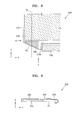
- FIG. 1 is a schematic plan view illustrating an area of a display apparatus according to an embodiment of the present invention.
- FIG. 2 is a side view of the area of FIG. 1 viewed from a direction A.
- the display apparatus 100 includes a display panel 110, an optical functional layer 120, a circuit member (or a circuit) 130, and a reinforcement member (or a reinforcement) 140.
- the display panel 110 may include one or more display devices to form an image toward a user's side (e.g., to project an image in the direction of the user).
- the display panel 110 may include a display device such as an organic light emitting device or a liquid crystal display device.
- the display panel 110 may also include one or more of other various suitable display devices.
- the display device of the display panel 110 will be described later with reference to FIGS. 3 and 4 .
- the optical functional layer 120 is disposed to face a surface of the display panel 110, for example, an upper surface of the display panel 110.
- the optical functional layer 120 is disposed such that a visible ray generated within the display panel 110 passes through the optical functional layer 120.
- the optical functional layer 120 improves image quality characteristics of the display panel 110.
- the optical functional layer 120 may be a polarization layer. According to another example embodiment, the optical functional layer 120 may be a film-type polarization layer.
- the circuit member 130 is formed to overlap with at least one edge of the display panel 110.
- the circuit member 130 may transmit an electrical signal used to operate the display panel 110, for example, to operate the display device of the display panel 110, to the display panel 110.
- an integrated circuit (IC) (not shown) that applies an electrical signal to the display panel 110 may be formed on a surface of the display panel 110, and the circuit member 130 may be disposed to be electrically connected to the IC.
- an end of the circuit member 130 may be connected to a circuit board (not shown) to receive an electrical signal from the circuit board and transmit the electrical signal to the IC or receive an electrical signal from the IC and transmit the electrical signal to the circuit board.
- the circuit member 130 may include a flexible material.
- the circuit member 130 may be a flexible printed circuit (FPC).
- the circuit member 130 may be a chip-on-film (COF).
- the circuit member 130 may be a flexible printed circuit board (FPCB).
- an end of the circuit member 130 may be curved as illustrated in FIG. 2 so that a portion of the circuit member 130 is disposed to face an opposite surface of the display panel 110 to the surface of the display panel 110 facing the optical functional layer 120.
- the reinforcement member 140 is disposed on a surface of the display panel 110 facing the optical functional layer 120, that is, on an upper surface of the display panel 110.
- the display panel 110 includes a first area 110a that is not overlapped with the optical functional layer 120 and the circuit member 130.
- the first area 110a is an area including at least one edge of the display panel 110.
- the reinforcement member 140 is disposed in the first area 110a so as not to overlap with the circuit member 130 and the optical functional layer 120.
- the reinforcement member 140 may be spaced apart from the optical functional layer 120 and the circuit member 130.
- the reinforcement member 140 may be formed to abut a side surface of the optical functional layer 120 or a side surface of the circuit member 130.
- the reinforcement member 140 is formed in the first area 110a, and the first area 110a is an area including an edge of the display panel 110.
- An edge area of the display panel 110 may be a point (or location) where cracks are generated or propagated if, for example, an external force is applied to the display panel 110.
- the reinforcement member 140 may be disposed adjacent to an edge of the display panel 110 so as to reduce generation or propagation of cracks or to prevent the same according to circumstances.
- the reinforcement member 140 may be formed of one or more of various suitable materials, may be formed of an organic material, and according to an example embodiment, the reinforcement member 140 may be formed of an organic material including an adhesive material.
- the reinforcement member 140 may be formed in the form of an adhesive tape and may be attached (e.g., easily attached) to the display panel 110.
- the reinforcement member 140 may include the same or substantially the same material as that of the display panel 110.
- the reinforcement member 140 may have various thicknesses, and may have a thickness such that steps generated due to the optical functional layer 120 included in the display apparatus 100 may be compensated.
- an extension line of an uppermost surface of the reinforcement member 140 may correspond to an extension line of an uppermost surface of the optical functional layer 120.
- the uppermost surfaces of the optical functional layer 120 and the reinforcement member 140 may be co-planar or substantially co-planar.
- the extension line of the uppermost surface of the reinforcement member 140 may be slightly below or slightly above the extension line of the uppermost surface of the optical functional layer 120, such that the uppermost surfaces are close to being co-planar.
- the display panel 110 may have various suitable forms, and will be described with reference to FIGS. 3 and 4 .
- FIG. 3 is an expanded view of a portion J of FIG. 2
- FIG. 4 illustrates a modified example of the portion J of FIG. 3 .
- the display panel 110 includes a substrate 101, an encapsulation member (or an encapsulation) 102, and a display device DU.
- the substrate 101 may be formed of one or more of various suitable materials.
- the substrate 101 may be formed of a glass material including SiO 2 as a main component.
- the substrate 101 may be formed of a flexible material such as a plastic material.
- the substrate 101 may be formed of a metal.
- the encapsulation member 102 is disposed to face the substrate 101.
- the encapsulation member 102 may also be formed of the same or substantially the same material as that of the substrate 101, for example, a glass material including SiO 2 as a main component.
- the substrate 101 may be formed of a flexible material such as a plastic material.
- the display device DU may be disposed between the substrate 101 and the encapsulation member 102.
- the display device DU may have one or more of various suitable forms to generate a visible ray.
- the display device DU may include an organic light emitting device, and the organic light emitting device includes a first electrode, a second electrode, and an intermediate layer disposed between the first and second electrodes.
- the intermediate layer includes an organic emissive layer that emits at least a visible ray.
- the first electrode (not shown) may function as an anode, and the second electrode (not shown) may function as a cathode, and polarities of the first and second electrodes may also be opposite.
- the first electrode may include ITO, IZO, ZnO, or In 2 O 3 having a high work function. Also, the first electrode may further include a reflective layer formed of, for example, Ag, Mg, Al, Pt, Pd, Au, Ni, Nd, Ir, Cr, Li, Yb or Ca according to purpose and design conditions.
- the second electrode may be formed of a metal such as Ag, Mg, Al, Pt, Pd, Au, Ni, Nd, Ir, Cr, Li, or Ca. Also, the second electrode may include ITO, IZO, ZnO, or In 2 O 3 so that light may transmit therethrough.
- the intermediate layer (not shown) includes at least an emissive layer to emit a visible ray.
- the intermediate layer includes an organic emissive layer and may additionally selectively include one or more of a hole injection layer, a hole transport layer, an electron transport layer, and an electron injection layer.
- the displays panel 110 may include at least one thin film transistor (not shown) that is electrically connected to an organic light emitting device. Also, the display panel 110 may include at least one capacitor that is electrically connected to the organic light emitting device.
- a sealing member SM may be disposed to adhere the substrate 101 and the encapsulation member 102.
- the sealing member SM may be disposed, for example, around the display device DU disposed between the substrate 101 and the encapsulation member 102 to adhere the substrate 101 and the encapsulation member 102 to each other.
- the optical functional layer 120 described above may be disposed on an upper surface of the encapsulation member 102.
- the encapsulation member 102 may not cover an area of a surface of the substrate 101. That is, in the first area 110a of the display panel 110 described above, an area of the substrate 101 may not be covered by the encapsulation member 102 but may be exposed.
- the encapsulation member 102 may be smaller than the substrate 101.
- the reinforcement member 140 may be formed on a surface of the substrate 101. As described above, the reinforcement member 140 may be formed to have an uppermost surface that corresponds to or almost corresponds to an extension line of an uppermost surface of the optical functional layer 120 so as to compensate for a step due to the optical functional layer 120. In other words, the uppermost surfaces of the optical functional layer 120 and the reinforcement member 140 may be co-planar or close to being co-planar. In the described embodiment, a thickness of the reinforcement member 140 may be greater than a thickness of the optical functional layer 120 as illustrated in FIG. 3 .
- the reinforcement member 140 may be formed not only in an area of the substrate 101 but also in an area of the encapsulation member 102.
- the first area 110a of the display panel 110 may be an area of the encapsulation member 102. That is, the encapsulation member 102 may have almost the same or substantially the same size as the substrate 101 so that an area of the substrate 101 may not be exposed or may be hardly exposed.
- the first area 110a may be an area of an upper surface of the encapsulation member 102 and the reinforcement member 140 may be formed on an upper surface of the encapsulation member 102.
- the reinforcement member 140 may be formed of the same or substantially the same material as that of the encapsulation member 102.
- the encapsulation member 102 may include a thin film or a film-type element.
- the encapsulation member 102 may include at least one organic layer or at least one inorganic layer.
- the encapsulation member 102 may have a structure in which at least one organic layer and at least one inorganic layer are alternately stacked at least once.
- the encapsulation member 102 may not cover an area of a surface of the substrate 101. That is, an area of a surface of the substrate 101 may not be covered by the encapsulation member 102 but may be exposed.
- the encapsulation member 102 may be smaller than the substrate 101. That is, in the described embodiment, in the first area 110a of the display panel 110, an area of the substrate 101 may not be covered by the encapsulation member 102 but may be exposed.
- the first area 110a of the display panel 110 may be an area of the encapsulation member 102. That is, the encapsulation member 102 may have almost the same or substantially the same size as the substrate 101 so that an area of the substrate 101 may not be exposed or may be hardly exposed.
- the first area 110a may be an area of an upper surface of the encapsulation member 102 or the reinforcement member 140 may be formed on the upper surface of the encapsulation member 102.
- the reinforcement member 140 may include the same or substantially the same material as that of the substrate 101 or the encapsulation member 102.
- the reinforcement member 140 when the substrate 101 is formed of a plastic material having flexibility, for example, when the substrate 101 includes polyethylene terephthalate (PET), the reinforcement member 140 may be formed to include PET. Accordingly, if an external force is applied to the substrate 101, the reinforcement member 140 may effectively buffer a stress applied to the substrate 101 so as to effectively reduce or block generation or propagation of cracks that may be caused to the substrate 101 or the display panel 110 including the substrate 101.
- PET polyethylene terephthalate
- FIG. 5 illustrates a modified example of the area of FIG. 2 .
- a display apparatus 100' illustrated in FIG. 5 includes a display panel 110', an optical functional layer 120', a circuit member (or a circuit) 130', a reinforcement member (or a reinforcement) 140', a touch panel 160', and a cover member (or a cover) 170'.
- a display panel 110' an optical functional layer 120'
- a circuit member 130' a circuit member 130'
- a reinforcement member 140' a reinforcement
- touch panel 160' a touch panel 160'
- cover member or a cover 170'.
- the display panel 110', the optical functional layer 120', the circuit member 130', and the reinforcement member 140' are the same or substantially the same as those described in the above-described embodiment, and thus detailed description thereof will be omitted.
- the touch panel 160' is disposed on the optical functional layer 120'.
- the touch panel 160' may include at least one touch pattern so as to recognize a touch of a user, and this will be described later with reference to FIGS. 6 and 7 .
- an adhesion member 150' may be disposed between the touch panel 160' and the optical functional layer 120', and the adhesion member 150' may be formed such that at least a portion of light generated within the display panel 110' is transmitted through the adhesion member 150'.
- the cover member 170' is disposed on the touch panel 160'. Accordingly, the touch panel 160' is disposed between the cover member 170' and the display panel 110' or between the cover member 170' and the optical functional layer 120'. According to an example embodiment, according to circumstances, the cover member 170' may be omitted. Also, the touch panel 160' may be omitted and the cover member 170' may be disposed on the display panel 110'.
- the cover member 170' prevents or reduces damages due to an impact applied to the display panel 110' or the touch panel 160', thereby improving durability of the display panel 110'.
- the cover member 170' may be formed of one or more of various suitable materials, for example, of a glass material or a plastic material. According to an example embodiment, when light generated within the display panel 110' is transmitted to the user's side through the cover member 170', the cover member 170' may be formed of a light-transmissive material.
- an adhesive material (not shown) may be disposed between the cover member 170' and the display panel 110'.
- a light blocking layer 171' may be formed in an area of the cover member 170' that is not covered by the touch panel 160'.
- the reinforcement member 140' may be disposed to correspond to space between the display panel 110' and the touch panel 160'. Accordingly, an area of the display panel 110' corresponding to the space between the touch panel 160' and the display panel 110' may be prevented or substantially prevented from being damaged due to an external force, or generation or propagation of cracks due to an external force may be effectively reduced, blocked, or substantially blocked.
- the reinforcement member 140' may be disposed to correspond to space between the display panel 110' and the cover member 170'. Accordingly, an area of the display panel 110' corresponding to the space between the cover member 170' and the display panel 110' may be prevented or substantially prevented from being damaged due to an external force, or generation or propagation of cracks due to an external force may be effectively reduced, blocked, or substantially blocked.
- FIG. 6 is an expanded view of a portion K of FIG. 5
- FIG. 7 illustrates a modified example of the portion K of FIG. 6 .
- the touch panel 160' may have one or more of various suitable forms. Referring to FIG. 6 , the touch panel 160' includes a base member 161' and a touch pattern 162'.
- the touch pattern 162' may be formed on an upper surface of the base member 161'. That is, the touch pattern 162' may be formed on a surface of the base member 161'facing the cover member 170'.
- the touch pattern 162' may be formed on a lower surface of the base member 161', that is, on a surface of the base member 161'facing the display panel 110'.
- the touch pattern 162' may have one or more of various suitable forms. That is, the touch pattern 162' may include a single conductive pattern or a plurality of conductive pattern layers, or may include two or more conductive pattern layers with at least one insulation layer included (or located) therebetween.
- the touch pattern 162' may be formed at least on a surface of an encapsulation member (or an encapsulation).
- FIG. 8 is a schematic plan view illustrating an area of a display apparatus 200 according to another embodiment of the present invention.
- the display apparatus 200 includes a display panel 210, an optical functional layer 220, a circuit member (or a circuit) 230, and a reinforcement member (or a reinforcement) 240.
- the display apparatus 200 may be bent with respect to a bending axis BL. Alternatively, the display apparatus 200 may be maintained in a bent state with respect to the bending axis BL.
- the display apparatus 200 includes a bending area with respect to the bending axis BL.
- the display panel 210 may include at least one display device to form an image toward a user's side.
- the display panel 210 may include a display device such as an organic light emitting device or a liquid crystal display device.
- the display panel 210 may also include one or more of other various suitable display devices.
- the optical functional layer 220 is disposed to face a surface of the display panel 210, for example, an upper surface of the display panel 210.
- the optical functional layer 220 is disposed such that a visible ray generated within the display panel 210 passes through the optical functional layer 220.
- the optical functional layer 220 improves image quality characteristics of the display panel 210.
- the optical functional layer 220 may be a polarization layer. According to another example embodiment, the optical functional layer 220 may be a film-type polarization layer.
- the circuit member 230 is formed to overlap with at least one edge of the display panel 210.
- the circuit member 230 may transmit an electrical signal used to operate the display panel 210, for example, to operate the display device of the display panel 210, to the display panel 210.
- an integrated circuit (IC) (not shown) that applies an electrical signal to the display panel 210 may be formed on a surface of the display panel 210, and the circuit member 230 may be disposed to be electrically connected to the IC.
- an end of the circuit member 230 may be connected to a circuit board (not shown) to receive an electrical signal from the circuit board and transmit the electrical signal to the IC or receive an electrical signal from the IC and transmit the electrical signal to the circuit board.
- the circuit member 230 may include a flexible material.
- the circuit member 230 may be an FPC.
- the circuit member 230 may be an FPCB.
- the circuit member 230 may be a chip-on-film (COF).
- an end of the circuit member 230 may be curved as illustrated in FIG. 9 so that a portion of the circuit member 230 is disposed to face an opposite surface to the surface of the display panel 210 facing the optical functional layer 220.
- the reinforcement member 240 is disposed on a surface of the display panel 210 facing the optical functional layer 220, that is, on an upper surface of the display panel 210.
- the display panel 210 includes a first area 210a that is not overlapped with the optical functional layer 220 and the circuit member 230.
- the first area 210a is an area including at least one edge of the display panel 210.
- the display panel 210 includes a cutting portion CL in at least an area of an edge thereof.
- the cutting portion CL is an area where a cutting process is performed when forming the display panel 210, and when manufacturing the display apparatus 200 by using the display panel 210, the cutting portion CL improves space utilization efficiency for disposing other elements (not shown) of the display panel apparatus 200.
- the cutting portion CL may be formed at various positions. According to an example embodiment, the cutting portion CL may be formed in a corner area of an edge area of the display panel 210, that is, in an area where two edges of the display panel 210 meet each other.
- the display panel 210 may include a substrate (not shown) and an encapsulation member (or an encapsulation, not shown) as described above, and the cutting portion CL may be formed on the substrate. According to an example embodiment, the cutting portion CL may be formed on the encapsulation member.
- the cutting portion CL may be overlapped with the bending axis BL.
- the cutting portion CL is included in the first area 210a. That is, the cutting portion CL may be formed in an area that is not overlapped with the optical functional layer 220 and the circuit member 230.
- the reinforcement member 240 may be disposed in the first area 210a so as not to be overlapped with the circuit member 230 and the optical functional layer 220.
- the reinforcement member 240 may be spaced apart from the optical functional layer 220 and the circuit member 230.
- the reinforcement member 240 may be formed to abut a side surface of the optical functional layer 220 or a side surface of the circuit member 230.
- the reinforcement member 240 may overlap with the bending axis BL.
- the reinforcement member 240 is formed in the first area 210a, and the first area 210a is an area including an edge of the display panel 210.
- An edge area of the display panel 210 may be a point where cracks are generated or propagated if, for example, an external force is applied to the display panel 210.
- the reinforcement member 240 is disposed adjacent to the edge of the display panel 210 so as to reduce generation or propagation of cracks, or to prevent or substantially prevent the same according to circumstances.
- the reinforcement member 240 may be disposed adjacent to the cutting portion CL as much as possible. Also, according to an example embodiment, a width of the reinforcement member 240 in at least a direction may correspond to or be greater than a length of the cutting portion CL.
- the cutting portion CL is an area among edge areas of the display panel 210 where high stresses are generated due to an external force, and thus cracks are more likely to be generated.
- the reinforcement member 240 may effectively support the cutting portion CL and mitigate stresses in the cutting portion CL, thereby reducing generation or propagation of cracks or preventing or substantially preventing the same according to circumstances.
- the reinforcement member 240 may be formed to have a parallel edge to a boundary line of the cutting portion CL.
- the display apparatus 200 may have a planar shape as illustrated in FIG 10A , but may also have a bent (or curved) shape as illustrated in FIG. 10B .
- the display apparatus 200 may maintain a bent (or curved) shape or may have a bent (or curved) shape only when desired according to user's convenience.
- the display apparatus 200 may include at least one bending axis BL.
- the bending axis BL may overlap with the cutting portion CL.
- the reinforcement member 240 may effectively mitigate stress applied to the cutting portion CL even if the display apparatus 200 is bent with respect to the bending axis BL, thereby reducing generation and propagation of the cracks.
- the reinforcement member 240 may overlap with the bending axis BL, and is formed in an area of a bending area, accordingly.
- the reinforcement member 240 may reduce the step formed due to the optical functional layer 220, thereby reducing the stress in the cutting portion CL and effectively reducing, substantially preventing, or preventing generation or propagation of cracks.
- the reinforcement member 240 may be formed of one or more of various suitable materials, for example, an organic material. According to an example embodiment, the reinforcement member 240 may be formed of an organic material including an adhesive material.
- the reinforcement member 240 may be formed in the form of an adhesive tape and may be attached (e.g., easily attached) to the display panel 210.
- the reinforcement member 240 may include the same or substantially the same material as that of the display panel 210.
- the reinforcement member 240 may have various thicknesses, and may have a thickness such that steps generated due to the optical functional layer 220 included in the display apparatus 200 may be compensated.
- an extension line of an uppermost surface of the reinforcement member 240 may correspond to an extension line of an uppermost surface of the optical functional layer 220, such that the uppermost surfaces of the optical functional layer 220 and the reinforcement member 240 may be co-planar or substantially co-planar with each other.
- the extension line of the uppermost surface of the reinforcement member 240 may be slightly below or slightly above the extension line of the uppermost surface of the optical functional layer 220, such that the uppermost surfaces of the optical functional layer 220 and the reinforcement member 240 may be close to being co-planar.
- the display panel 210 in some embodiments may selectively include a structure of FIGS. 3 and 4 described above.
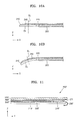
- FIG. 11 illustrates a modified example of the area of FIG. 9 .
- a display apparatus 200' illustrated in FIG. 11 includes a display panel 210', an optical functional layer 220', a circuit member (or a circuit) 230', a reinforcement member (or a reinforcement) 240', a touch panel 260', and a cover member (or a cover) 270'.
- a display panel 210' an optical functional layer 220'
- a circuit member (or a circuit) 230' a reinforcement member (or a reinforcement) 240'
- a touch panel 260' a touch panel 260'
- cover member or a cover
- the display panel 210', the optical functional layer 220', the circuit member 230', and the reinforcement member 240', are the same or substantially the same as those described in the above-described embodiment of FIG. 9 , and thus detailed description thereof will be omitted.
- the touch panel 260' is disposed on the optical functional layer 220'.
- the touch panel 260' may include at least one touch pattern to recognize a touch of a user, and the structure of the touch panel 260' is the same or substantially the same as that described with reference to FIGS. 6 and 7 .
- an adhesion member 250' may be disposed between the touch panel 260' and the optical functional layer 220', and the adhesion member 250' may be formed such that at least a portion of light generated within the display panel 210' is transmitted through the adhesion member 250'.
- the cover member 270' is disposed on the touch panel 260'. Accordingly, the touch panel 260' is disposed between the cover member 270' and the display panel 210' or between the cover member 270' and the optical functional layer 220'. According to an example embodiment, according to circumstances, the cover member 270' may be omitted. Also, the touch panel 260' may be omitted and the cover member 270' may be disposed on the display panel 210'.
- the cover member 270' prevents or substantially prevents damages due to an impact applied to the display panel 210' or the touch panel 260', thereby improving durability of the display panel 210'.
- the cover member 270' may be formed of one or more of various suitable materials, for example, of a glass material or a plastic material. According to an example embodiment, when light generated within the display panel 210' is transmitted to the user's side through the cover member 270', the cover member 270' may be formed of a light-transmissive material.
- an adhesive material (not shown) may be disposed between the cover member 270' and the display panel 210'.
- a light blocking layer 271' may be formed in an area of the cover member 270' that is not covered by the touch panel 260'.
- the reinforcement member 240' may be disposed to correspond to space between the display panel 210' and the touch panel 260'. Accordingly, an area of the display panel 210' corresponding to the space between the touch panel 260' and the display panel 210' may be prevented or substantially prevented from being damaged due to an external force, or generation or propagation of cracks due to an external force may be effectively reduced, substantially blocked, or blocked.
- the reinforcement member 240' may be disposed to correspond to space between the display panel 210' and the cover member 270'. Accordingly, an area of the display panel 210' corresponding to the space between the cover member 270' and the display panel 210' may be prevented or substantially prevented from being damaged due to an external force, or generation or propagation of cracks due to an external force may be effectively reduced, substantially blocked, or blocked.
- the touch panel 260' may selectively include the structure illustrated in FIGS. 6 and 7 .
- the touch panel 260' may include a base member (not shown) and a touch pattern (not shown), and the touch pattern may be formed on an upper surface or a lower surface of the base member.
- FIG. 12 is a schematic plan view illustrating an area of a display apparatus 300 according to another embodiment of the present invention.
- the display apparatus 300 includes a display panel 310, an optical functional layer 320, a circuit member (or a circuit) 330, and a reinforcement member (or a reinforcement) 340.
- the display apparatus 300 may be bent with respect to a bending axis (not shown). Alternatively, the display apparatus 300 may be maintained in a bent state with respect to a bending axis (not shown). According to an example embodiment, the display apparatus 300 may be bent with respect to two bending axes (not shown), and may include cutting portions CL1 and CL2 that overlap with a bending axis (not shown).
- the display panel 310 may include at least one display device to form an image toward a user's side.
- the display panel 310 may include a display device such as an organic light emitting device or a liquid crystal display device.
- the display panel 310 may also include one or more of other various suitable display devices.
- the optical functional layer 320 is disposed to face a surface of the display panel 310, for example, an upper surface of the display panel 310.
- the optical functional layer 320 is disposed such that a visible ray generated within the display panel 310 passes through the optical functional layer 320.
- the optical functional layer 320 improves image quality characteristics of the display panel 310.
- the optical functional layer 320 may be a polarization layer. According to another example embodiment, the optical functional layer 320 may be a film-type polarization layer.
- the circuit member 330 is formed to overlap with at least one edge of the display panel 310.
- the circuit member 330 may transmit an electrical signal used to operate the display panel 310, for example, to operate the display device of the display panel 310, to the display panel 310.
- an integrated circuit (IC) (not shown) that applies an electrical signal to the display panel 310 may be formed on a surface of the display panel 310, and the circuit member 330 may be disposed to be electrically connected to the IC.
- an end of the circuit member 330 may be connected to a circuit board (not shown) to receive an electrical signal from the circuit board and transmit the electrical signal to the IC or receive an electrical signal from the IC and transmit the electrical signal to the circuit board.
- the circuit member 330 may include a flexible material.
- the circuit member 330 may be an FPC.
- the circuit member 330 may be an FPCB.
- the circuit member 330 may be a chip-on-film (COF).
- the reinforcement member 340 is disposed on a surface of the display panel 310 facing the optical functional layer 320, that is, on an upper surface of the display panel 310.
- the reinforcement member 340 includes a first reinforcement member (or a first reinforcement) 341 and a second reinforcement member (or a second reinforcement) 342.
- the display panel 310 includes a first area 310a that is not overlapped with the optical functional layer 320 and the circuit member 330.
- the first area 310a is an area including at least one edge of the display panel 310.
- the first reinforcement member 341 and the second reinforcement member 342 of the reinforcement member 340 are disposed in the first area 310a at two sides with the circuit member 330 included (or located) therebetween.
- the display panel 310 includes first and second cutting portions CL1 and CL2 in at least two areas of an edge thereof.
- the first cutting portion CL1 and the second cutting portion CL2 are spaced apart from each other and may be formed at two sides with the circuit member 330 included (or located) therebetween.
- the first and second cutting portions CL1 and CL2 are areas where a cutting process is performed when forming the display panel 310, and when manufacturing the display apparatus 300 by using the display panel 310.
- the first and second cutting portions CL1 and CL2 improve space utilization efficiency for disposing other elements (not shown) of the display apparatus 300.
- the display panel 310 may also include a substrate (not shown) and an encapsulation member (or an encapsulation, not shown), and the first cutting portion CL1 and the second cutting portion CL2 may be formed on the substrate. According to an example embodiment, the first cutting portion CL1 and the second cutting portion CL2 may be formed on the encapsulation member.
- the first cutting portion CL1 and the second cutting portion CL2 may be formed at two corners of an edge area of the display panel 310. According to an example embodiment, the first cutting portion CL1 and the second cutting portion CL2 may overlap with a bending axis (not shown).
- the first cutting portion CL1 and the second cutting portion CL2 are included in the first area 310a. That is, the first cutting portion CL1 and the second cutting portion CL2 may be formed in an area that is not overlapped with the optical functional layer 320 and the circuit member 330.
- the first reinforcement member 341 and the second reinforcement member 342 of the reinforcement member 340 are disposed in the first area 310a and thus do not overlap with the circuit member 330 and the optical functional layer 320.
- the reinforcement member 340 may be spaced apart from the optical functional layer 320 and the circuit member 330.
- the reinforcement member 340 may be formed to abut a side surface of the optical functional layer 320 or a side surface of the circuit member 330.
- the reinforcement member 340 is formed in the first area 310a, and the first area 310a is an area including an edge of the display panel 310.
- An edge area of the display panel 310 may be a point where cracks are generated or propagated if, for example, an external force is applied to the display panel 310.
- the reinforcement member 340 is disposed adjacent to an edge of the display panel 310 so as to reduce generation or propagation of cracks or prevent or substantially prevent the same according to circumstances.
- the reinforcement member 340 may be disposed adjacent to the first and second cutting portions CL1 and CL2 as much as possible. That is, the first reinforcement member 341 may be disposed adjacent to the first cutting portion CL1, and according to an example embodiment, a width of the first reinforcement member 341 in at least a direction may correspond to a length of the first cutting portion CL1.
- the second reinforcement member 342 may be disposed adjacent to the second cutting portion CL2, and according to an example embodiment, a width of the second reinforcement member 342 in at least a direction may correspond to a length of the second cutting portion CL2.
- the first reinforcement member 341 may be formed to have a parallel edge to a boundary line of the first cutting portion CL1
- the second reinforcement member 342 may be formed to have a parallel edge to a boundary line of the second cutting portion CL2.
- the display apparatus 300 may have a planar shape or a bent (or curved) shape as illustrated in FIG 10A and in FIG. 10B .
- the reinforcement member 340 may be formed of one or more of various suitable materials, for example, an organic material. According to an example embodiment, the reinforcement member 340 may be formed of an organic material including an adhesive material.
- the reinforcement member 340 may be formed in the form of an adhesive tape and may be attached (e.g., easily attached) to the display panel 310.
- the reinforcement member 340 may include the same or substantially the same material as that of the display panel 310.
- the reinforcement member 340 may have various thicknesses, and may have a thickness such that steps generated due to the optical functional layer 320 included in the display apparatus 300 may be compensated.
- an extension line of an uppermost surface of the reinforcement member 340 may correspond to an extension line of an uppermost surface of the optical functional layer 320, such that the uppermost surfaces of the optical functional layer 320 and the reinforcement member 340 may be co-planar or substantially co-planar.
- the extension line of the uppermost surface of the reinforcement member 340 may be slightly below or slightly above the extension line of the uppermost surface of the optical functional layer 320, such that the uppermost surfaces of the optical functional layer 320 and the reinforcement member 340 may be close to being co-planar.
- the display panel 310 in some embodiments may selectively include the structure of FIGS. 3 and 4 described above.
- the display apparatus 300 may include a touch panel (not shown) or a cover member (or cover, not shown) as illustrated in FIG. 11 .
- the touch panel included in the display apparatus 300 has the same or substantially the same structure as that of FIGS. 6 and 7 described above.
- FIG. 13 is a schematic plan view illustrating an area of a display apparatus 400 according to another embodiment of the present invention
- FIG. 14 is a side view of the area of FIG. 13 viewed from a direction B.
- the display apparatus 400 includes a display panel 410, an optical functional layer 420, a reinforcement member (or a reinforcement) 440, a touch panel 460, and a touch circuit member (or a touch circuit) 435 for transmitting a signal to the touch panel 460.
- a reinforcement member or a reinforcement
- a touch panel 460 for transmitting a signal to the touch panel 460.
- a touch circuit member or a touch circuit
- the display apparatus 400 may be bent with respect to a bending axis (not shown). Alternatively, the display apparatus 400 may be maintained in a bent state with respect to a bending axis (not shown). According to an example embodiment, the display apparatus 400 may be bent with respect to two bending axes (not shown), and may include cutting portions CL1 and CL2 that overlap with a bending axis (not shown).
- the display panel 410 may include at least one display device to form an image toward a user's side.
- the display panel 410 may include a display device such as an organic light emitting device or a liquid crystal display device.
- the display panel 410 may also include one or more of other various suitable display devices.
- the optical functional layer 420 is disposed to face a surface of the display panel 410, for example, an upper surface of the display panel 410.
- the optical functional layer 420 is disposed such that a visible ray generated within the display panel 410 passes through the optical functional layer 420.
- the optical functional layer 420 improves image quality characteristics of the display panel 410.
- the optical functional layer 420 may be a polarization layer.
- the optical functional layer 420 may be a film-type polarization layer.
- the circuit member 430 is formed to overlap with at least one edge of the display panel 410.
- the circuit member 430 may transmit an electrical signal used to operate the display panel 410, for example, to operate the display device of the display panel 410, to the display panel 410.
- an integrated circuit (IC) (not shown) that applies an electrical signal to the display panel 410 may be formed on a surface of the display panel 410, and the circuit member 430 may be disposed to be electrically connected to the IC.
- an end of the circuit member 430 may be connected to a circuit board (not shown) to receive an electrical signal from the circuit board and transmit the electrical signal to the IC or receive an electrical signal from the IC and transmit the electrical signal to the circuit board.
- the circuit member 430 may include a flexible material.
- the circuit member 430 may be an FPC.
- the circuit member 430 may be an FPCB.
- the circuit member 430 may be a chip-on-film (COF).
- the touch panel 460 is disposed on the optical functional layer 420.
- the touch panel 460 may include at least one touch pattern to recognize a touch of a user, and an example of the touch panel 460 is the same or substantially the same as that illustrated in FIGS. 6 and 7 .
- an adhesion member 450 may be disposed between the touch panel 460 and the optical functional layer 420, and the adhesion member 450 may be formed such that at least a portion of light generated within the display panel 410 is transmitted through the adhesion member 450.
- the touch circuit member 435 is formed to transmit an electrical signal to the touch panel 460. According to an exemplary embodiment, the touch circuit member 435 may transmit an electrical signal to the touch panel 460.
- the touch circuit member 435 may be electrically connected to the touch panel 460 via a wiring (not shown) or a conductive pattern (not shown).
- the touch circuit member 435 may have various suitable forms and/or of various suitable types. According to an example embodiment, the touch circuit member 435 may include a flexible material.
- the touch circuit member 435 may be an FPC.
- the touch circuit member 435 may be an FPCB.
- An end of the touch circuit member 435 which is flexible may be curved so that a portion of the touch circuit member 435 faces an opposite surface to a surface of the display panel 410 that faces the touch panel 460.
- a cover member 470 is disposed on the touch panel 460. Accordingly, the touch panel 460 is disposed between the cover member 470 and the display panel 410 or between the cover member 470 and the optical functional layer 420. According to an example embodiment, the cover member 470 may be omitted according to circumstances.
- the cover member 470 prevents or substantially prevents damages due to an impact applied to the display panel 410 or the touch panel 460, thereby improving durability of the display panel 410.
- the cover member 470 may be formed of one or more of various suitable materials, for example, of a glass material or a plastic material. According to an example embodiment, when light generated within the display panel 410 is transmitted to the user's side through the cover member 470, the cover member 470 may be formed of a light-transmissive material.
- an adhesive material (not shown) may be disposed between the cover member 470 and the display panel 410.
- a light blocking layer 471 may be formed in an area of the cover member 470 that is not covered by the touch panel 460.
- the reinforcement member 440 is disposed on a surface of the display panel 410 facing the optical functional layer 420, that is, on an upper surface of the display panel 410.
- the reinforcement member 440 includes a first reinforcement member (or a first reinforcement) 441 and a second reinforcement member (or a second reinforcement) 442.
- the display panel 410 includes a first area 410a that is not overlapped with the optical functional layer 420, the circuit member 430, and the touch circuit member 435.
- the first area 410a is an area including at least one edge of the display panel 410.
- the first reinforcement member 441 and the second reinforcement member 442 of the reinforcement member 440 are disposed in the first area 410a and at two sides with the circuit member 430 and the touch circuit member 435 included (or located) therebetween.
- the display panel 410 includes first and second cutting portions CL1 and CL2 in at least two areas of an edge thereof.
- the first cutting portion CL1 and the second cutting portion CL2 are spaced apart from each other and may be formed at two sides with the circuit member 430 and the touch circuit member 435 included (or located) therebetween.
- the display panel 410 may also include a substrate (not shown) and an encapsulation member (or an encapsulation, not shown), and the first cutting portion CL1 and the second cutting portion CL2 may be formed on the substrate.
- the first cutting portion CL1 and the second cutting portion CL2 may be formed on the encapsulation member.
- the first cutting portion CL1 and the second cutting portion CL2 may overlap with a bending axis (not shown).
- the first cutting portion CL1 and the second cutting portion CL2 are included in the first area 410a. That is, the first cutting portion CL1 and the second cutting portion CL2 may be formed in an area that is not overlapped with the optical functional layer 420, the circuit member 430, and the touch circuit member 435.
- the first reinforcement member 441 and the second reinforcement member 442 of the reinforcement member 440 are disposed in the first area 410a and thus do not overlap with the circuit member 430 and the touch circuit member 435 and the optical functional layer 420.
- the reinforcement member 440 may be spaced apart from the optical functional layer 420 and the touch circuit member 435.
- the reinforcement member 440 may be formed to abut a side surface of the optical functional layer 420 or a side surface of the circuit member 430 or a side surface of the touch circuit member 435.
- the reinforcement member 440 may be disposed adjacent to the first and second cutting portions CL1 and CL2 as much as possible. That is, the first reinforcement member 441 may be disposed adjacent to the first cutting portion CL1, and according to an example embodiment, a width of the first reinforcement member 441 in at least a direction may correspond to a length of the first cutting portion CL1.
- the second reinforcement member 442 may be disposed adjacent to the second cutting portion CL2, and according to an example embodiment, a width of the second reinforcement member 442 in at least a direction may correspond to a length of the second cutting portion CL2.
- the first reinforcement member 441 may be formed to have a parallel edge to a boundary line of the first cutting portion CL1
- the second reinforcement member 442 may be formed to have a parallel edge to a boundary line of the second cutting portion CL2.
- the display apparatus 400 may have a planar shape or a bent (or curved) shape as illustrated in FIG 10A and in FIG. 10B .
- the reinforcement member 440 may be formed of one or more of various suitable materials, for example, an organic material. According to an example embodiment, the reinforcement member 440 may be formed of an organic material including an adhesive material.
- the reinforcement member 440 may be formed in the form of an adhesive tape and may be attached (e.g., easily attached) to the display panel 410.
- the reinforcement member 440 may include the same or substantially the same material as that of the display panel 410.
- the reinforcement member 440 may have various thicknesses, and may have a thickness such that steps generated due to the optical functional layer 420 included in the display apparatus 400 may be compensated.
- an extension line of an uppermost surface of the reinforcement member 440 may correspond to an extension line of an uppermost surface of the optical functional layer 420, such that the uppermost surfaces of the optical functional layer 420 and the reinforcement member 440 may be co-planar or substantially co-planar.
- the extension line of the uppermost surface of the reinforcement member 440 may be slightly below or slightly above the extension line of the uppermost surface of the optical functional layer 420, such that the uppermost surfaces of the optical functional layer 420 and the reinforcement member 440 may be close to being co-planar.
- the display panel 410 in some embodiments may selectively include the structure of FIGS. 3 and 4 described above.
- FIG. 15 is a schematic plan view illustrating an area of a display apparatus 500 according to another embodiment of the present invention.
- the display apparatus 500 includes a display panel 510, an optical functional layer 520, a reinforcement member 540, and a circuit member 530. Although not illustrated, according to an example embodiment, the display apparatus 500 may include a touch panel (not shown), and may further include a touch circuit member (not shown).
- the display apparatus 500 may be bent with respect to a bending axis (not shown). Alternatively, the display apparatus 500 may be maintained in a bent state with respect to a bending axis (not shown). According to an example embodiment, the display apparatus 500 may be bent with respect to two bending axes (not shown), and may include cutting portions CL1 and CL2 that overlap with a bending axis (not shown).
- the display panel 510 may include one or more display devices to form an image toward a user's side.
- the display panel 510 may include a display device such as an organic light emitting device or a liquid crystal display device.
- the display panel 510 may also include one or more of other various suitable display devices.
- the optical functional layer 520 is disposed to face a surface of the display panel 510, for example, an upper surface of the display panel 510.
- the optical functional layer 520 is disposed such that a visible ray generated within the display panel 510 passes through the optical functional layer 520.
- the optical functional layer 520 improves image quality characteristics of the display panel 510.
- the optical functional layer 520 may be a polarization layer. According to another example embodiment, the optical functional layer 520 may be a film-type polarization layer.
- the circuit member 530 is formed to overlap with at least one edge of the display panel 510.
- the circuit member 530 may transmit an electrical signal used to operate the display panel 510, for example, to operate the display device of the display panel 510, to the display panel 510.
- an integrated circuit (IC) (not shown) that applies an electrical signal to the display panel 510 may be formed on a surface of the display panel 510, and the circuit member 530 may be disposed to be electrically connected to the IC.
- an end of the circuit member 530 may be connected to a circuit board (not shown) to receive an electrical signal from the circuit board and transmit the electrical signal to the IC or receive an electrical signal from the IC and transmit the electrical signal to the circuit board.
- the circuit member 530 may include a flexible material.
- the circuit member 530 may be an FPC.
- the circuit member 530 may be an FPCB.
- the reinforcement member 540 is disposed on a surface of the display panel 510 facing the optical functional layer 520, that is, on an upper surface of the display panel 510.
- the reinforcement member 540 includes a first reinforcement member (or a first reinforcement) 541 and a second reinforcement member (or a second reinforcement) 542.
- the first reinforcement member 541 and the second reinforcement member 542 are connected to the optical functional layer 520.
- the first reinforcement member 541 and the second reinforcement member 542 may be formed of the same or substantially the same material as that of the optical functional layer 520, and according to an exemplary embodiment, the first reinforcement member 541 and the second reinforcement member 542 may be formed as a single body with the optical functional layer 520.
- a pattern may be formed to extend to a first area 510a of the display panel 510 and to be disposed with the circuit member 530 included (or located) between the first reinforcement member 541 and the second reinforcement member 542, thereby forming (e.g., easily forming) the first reinforcement member 541 and the second reinforcement member 542.
- the display panel 510 includes the first area 510a that does not overlap with the optical functional layer 520 and the circuit member 530.
- the first area 510a is an area including at least an edge of the display panel 510.
- the first reinforcement member 541 and the second reinforcement member 542 of the reinforcement member 540 are disposed in the first area 510a and at two sides with the circuit member 530 and a touch circuit member (or a touch circuit) 535 included (or located) therebetween.
- the display panel 510 includes first and second cutting portions CL1 and CL2 in at least two areas of an edge thereof.
- the first cutting portion CL1 and the second cutting portion CL2 are spaced apart from each other and may be formed at two sides with the circuit member 520 included (or located) therebetween.
- the display panel 510 may also include a substrate (not shown) and an encapsulation member (or an encapsulation, not shown), and the first cutting portion CL1 and the second cutting portion CL2 may be formed on the substrate. According to an example embodiment, the first cutting portion CL1 and the second cutting portion CL2 may be formed on the encapsulation member.
- the first cutting portion CL1 and the second cutting portion CL2 may overlap with a bending axis (not shown).
- the first cutting portion CL1 and the second cutting portion CL2 are included in the first area 510a. That is, the first cutting portion CL1 and the second cutting portion CL2 may be formed in an area that is not overlapped with the optical functional layer 520 and the circuit member 530.
- the first reinforcement member 541 and the second reinforcement member 542 of the reinforcement member 540 are disposed in the first area 510a and thus do not overlap with the circuit member 530 and the optical functional layer 520.
- the reinforcement member 540 may be spaced apart from the circuit member 530.
- the reinforcement member 540 may be formed to abut a side surface of the circuit member 530.
- the reinforcement member 540 may be disposed adjacent to the first and second cutting portions CL1 and CL2 as much as possible. That is, the first reinforcement member 541 may be disposed adjacent to the first cutting portion CL1, and according to an example embodiment, a width of the first reinforcement member 541 in at least a direction may correspond to a length of the first cutting portion CL1.
- the second reinforcement member 542 may be disposed adjacent to the second cutting portion CL2, and according to an example embodiment, a width of the second reinforcement member 542 in at least a direction may correspond to a length of the second cutting portion CL2.
- the first reinforcement member 541 may be formed to have a parallel edge to a boundary line of the first cutting portion CL1
- the second reinforcement member 542 may be formed to have a parallel edge to a boundary line of the second cutting portion CL2.
- the display apparatus 500 may have a planar shape or a bent (or curved) shape as illustrated in FIG 10A and in FIG. 10B .
- the reinforcement member 540 may be formed of one or more of various suitable materials, for example, an organic material. According to an example embodiment, the reinforcement member 540 may be formed of an organic material including an adhesive material.
- the reinforcement member 540 may be formed in the form of an adhesive tape and may be attached (e.g., easily attached) to the display panel 510.
- the reinforcement member 540 may include the same or substantially the same material as that of the display panel 510.
- the reinforcement member 540 may have various thicknesses, and may have a thickness such that steps generated due to the optical functional layer 520 included in the display apparatus 500 may be compensated.
- an extension line of an uppermost surface of the reinforcement member 540 may correspond to an extension line of an uppermost surface of the optical functional layer 520, such that the uppermost surfaces of the optical functional layer 520 and the reinforcement member 540 may be co-planar or substantially co-planar.
- the extension line of the uppermost surface of the reinforcement member 540 may be slightly below or slightly above the extension line of the uppermost surface of the optical functional layer 520, such that the uppermost surfaces of the optical functional layer 520 and the reinforcement member 540 may be close to being co-planar.
- the display panel 510 in some embodiments may selectively include the structure of FIGS. 3 and 4 described above.
- the display apparatus 500 may include a touch panel (not shown) or a cover member (or a cover, not shown) as illustrated in FIG. 11 .
- the touch panel included in the display apparatus 500 has the same or substantially the same structure as that of FIGS. 6 and 7 described above.
- a structure including a touch circuit member (or a touch circuit, not shown) as illustrated in FIGS. 13 and 14 may be selectively applied.
- the optical functional layer 520 and the reinforcement member 540 are connected so as to improve durability of the display panel 510 by using the reinforcement member 540. That is, as the reinforcement member 540 is connected to the optical functional layer 520, a pressure applied to the display panel 510 is reduced first via the reinforcement member 540, and then a pressure transmitted to the reinforcement member 540 may also be partially transmitted to the optical functional layer 520. Thus, generation or propagation of cracks due to abnormal concentration of stress on the display panel 510 may be reduced, substantially prevented, or prevented as described above.
- the reinforcement member 540 is formed as a single body with the optical functional layer 520 so that the reinforcement member 540 may be formed (e.g., easily formed) without any additional process except formation of the optical functional layer 520.
- no gap is formed between the optical functional layer 520 and the reinforcement member 540.
- a gap might act as a path through which abnormal pressure may pass if an external force is applied to the display panel 510, and cracks may be suddenly generated due to the abnormal pressure.
- a structure according to the present embodiment in which the optical functional layer 520 and the reinforcement member 540 are formed as a single body may prevent (e.g., easily prevent) the above problem.
- durability of the display apparatus may be improved (e.g., easily improved).
Landscapes
- Physics & Mathematics (AREA)
- Nonlinear Science (AREA)
- General Physics & Mathematics (AREA)
- Engineering & Computer Science (AREA)
- Crystallography & Structural Chemistry (AREA)
- Chemical & Material Sciences (AREA)
- Optics & Photonics (AREA)
- Mathematical Physics (AREA)
- Theoretical Computer Science (AREA)
- General Engineering & Computer Science (AREA)
- Human Computer Interaction (AREA)
- Computer Hardware Design (AREA)
- Plasma & Fusion (AREA)
- Devices For Indicating Variable Information By Combining Individual Elements (AREA)
- Electroluminescent Light Sources (AREA)
Applications Claiming Priority (1)
| Application Number | Priority Date | Filing Date | Title |
|---|---|---|---|
| KR1020140117030A KR101797729B1 (ko) | 2014-09-03 | 2014-09-03 | 디스플레이 장치 |
Publications (3)
| Publication Number | Publication Date |
|---|---|
| EP3001243A2 true EP3001243A2 (de) | 2016-03-30 |
| EP3001243A3 EP3001243A3 (de) | 2016-07-13 |
| EP3001243B1 EP3001243B1 (de) | 2021-04-07 |
Family
ID=54146918
Family Applications (1)
| Application Number | Title | Priority Date | Filing Date |
|---|---|---|---|
| EP15182576.7A Active EP3001243B1 (de) | 2014-09-03 | 2015-08-26 | Anzeigevorrichtung |
Country Status (4)
| Country | Link |
|---|---|
| US (1) | US11209922B2 (de) |
| EP (1) | EP3001243B1 (de) |
| KR (1) | KR101797729B1 (de) |
| CN (1) | CN105389035B (de) |
Families Citing this family (7)
| Publication number | Priority date | Publication date | Assignee | Title |
|---|---|---|---|---|
| KR101797729B1 (ko) * | 2014-09-03 | 2017-11-16 | 삼성디스플레이 주식회사 | 디스플레이 장치 |
| US10664009B2 (en) * | 2017-01-20 | 2020-05-26 | Dell Products L.P. | Narrow border plastic cover with optimal opto-mechanical properties |
| KR102374561B1 (ko) * | 2017-06-19 | 2022-03-15 | 삼성디스플레이 주식회사 | 표시 장치 및 입력감지부재 |
| US10847908B2 (en) * | 2018-07-25 | 2020-11-24 | Sharp Kabushiki Kaisha | Connected board and display device |
| CN109377890B (zh) * | 2018-12-21 | 2020-01-21 | 武汉华星光电半导体显示技术有限公司 | 柔性显示装置 |
| KR102760149B1 (ko) * | 2019-11-04 | 2025-01-31 | 삼성디스플레이 주식회사 | 표시장치 |
| KR102879898B1 (ko) | 2020-08-05 | 2025-11-03 | 삼성디스플레이 주식회사 | 터치 감지 장치, 그를 포함하는 표시 장치, 및 그의 구동 방법 |
Family Cites Families (32)
| Publication number | Priority date | Publication date | Assignee | Title |
|---|---|---|---|---|
| TWI284230B (en) * | 2002-05-17 | 2007-07-21 | Merck Patent Gmbh | Compensator comprising a positive and a negative birefringent retardation film and use thereof |
| JP4938239B2 (ja) | 2004-04-23 | 2012-05-23 | シャープ株式会社 | 表示装置 |
| US20100045705A1 (en) * | 2006-03-30 | 2010-02-25 | Roel Vertegaal | Interaction techniques for flexible displays |
| JP2008070584A (ja) | 2006-09-14 | 2008-03-27 | Hitachi Displays Ltd | 液晶表示装置 |
| US20080094561A1 (en) * | 2006-10-19 | 2008-04-24 | Chih-Shun Fan | System for providing a flat display panel |
| JP4561729B2 (ja) | 2006-11-06 | 2010-10-13 | エプソンイメージングデバイス株式会社 | 電気光学装置及び電子機器 |
| US7786559B2 (en) * | 2006-11-08 | 2010-08-31 | Corning Incorporated | Bezel packaging of frit-sealed OLED devices |
| KR101481682B1 (ko) * | 2007-04-09 | 2015-01-12 | 삼성디스플레이 주식회사 | 터치스크린 표시장치 |
| KR20090037547A (ko) | 2007-10-12 | 2009-04-16 | 삼성전자주식회사 | 표시장치 |
| JP4917582B2 (ja) * | 2008-07-25 | 2012-04-18 | 住友化学株式会社 | アクティブマトリクス基板、ディスプレイパネル、表示装置およびアクティブマトリクス基板の製造方法 |
| JP2010072380A (ja) * | 2008-09-19 | 2010-04-02 | Hitachi Displays Ltd | 表示装置 |
| KR101521219B1 (ko) * | 2008-11-10 | 2015-05-18 | 엘지전자 주식회사 | 플렉서블 디스플레이를 이용하는 휴대 단말기 및 그 제어방법 |
| TW201110802A (en) * | 2009-06-24 | 2011-03-16 | Seiko Epson Corp | Electro-optical device, electronic device, and illumination apparatus |
| KR101309862B1 (ko) * | 2009-12-10 | 2013-09-16 | 엘지디스플레이 주식회사 | 터치 패널 일체형 액정 표시 장치 |
| KR20110091380A (ko) * | 2010-02-05 | 2011-08-11 | 삼성전자주식회사 | 터치 패널의 노이즈 보상 방법 및 장치 |
| TWI424388B (zh) | 2010-04-30 | 2014-01-21 | Au Optronics Corp | 可撓式顯示器及其製造方法 |
| KR101759577B1 (ko) * | 2010-08-23 | 2017-07-19 | 삼성전자 주식회사 | 온-셀 tsp 능동형유기발광다이오드 구조 |
| KR101216326B1 (ko) * | 2011-03-02 | 2012-12-27 | 하이디스 테크놀로지 주식회사 | 액정표시장치의 디스플레이 패널 및 그 제조방법 |
| US9400576B2 (en) | 2011-07-19 | 2016-07-26 | Apple Inc. | Touch sensor arrangements for organic light-emitting diode displays |
| US8804347B2 (en) * | 2011-09-09 | 2014-08-12 | Apple Inc. | Reducing the border area of a device |
| TWI468785B (zh) | 2011-11-30 | 2015-01-11 | Au Optronics Corp | 顯示模組 |
| KR20130089513A (ko) | 2012-02-02 | 2013-08-12 | 삼성디스플레이 주식회사 | 표시장치 |
| KR102013587B1 (ko) * | 2012-05-03 | 2019-08-23 | 엘지전자 주식회사 | 이동 단말기 및 그것의 제어방법 |
| KR101953249B1 (ko) * | 2012-05-09 | 2019-06-03 | 삼성디스플레이 주식회사 | 터치 감지 및 입체 영상 표시 겸용 표시 장치 및 그 구동 방법 |
| CN202661978U (zh) | 2012-06-12 | 2013-01-09 | 深圳市灵畅互动科技有限公司 | 一种触摸一体机的外框结构 |
| KR101373235B1 (ko) | 2012-06-29 | 2014-03-13 | (주)넥스디스플레이 | 단차 보상 테잎을 포함하는 백라이트 유닛 및 이를 포함하는 lcd 모듈 |
| CN103593080B (zh) | 2012-08-17 | 2016-11-23 | 宸鸿光电科技股份有限公司 | 触控模块及其制造方法 |
| TWI522857B (zh) * | 2013-10-11 | 2016-02-21 | 群創光電股份有限公司 | 觸控顯示面板、觸控顯示裝置及顯示裝置 |
| KR101797729B1 (ko) * | 2014-09-03 | 2017-11-16 | 삼성디스플레이 주식회사 | 디스플레이 장치 |
| KR102204378B1 (ko) * | 2014-09-04 | 2021-01-19 | 삼성디스플레이 주식회사 | 표시장치 및 그 구동방법 |
| US9287329B1 (en) * | 2014-12-30 | 2016-03-15 | Lg Display Co., Ltd. | Flexible display device with chamfered polarization layer |
| KR101913394B1 (ko) * | 2016-07-29 | 2018-10-31 | 삼성디스플레이 주식회사 | 표시 장치 |
-
2014
- 2014-09-03 KR KR1020140117030A patent/KR101797729B1/ko active Active
-
2015
- 2015-03-16 US US14/659,457 patent/US11209922B2/en active Active
- 2015-08-18 CN CN201510508323.6A patent/CN105389035B/zh active Active
- 2015-08-26 EP EP15182576.7A patent/EP3001243B1/de active Active
Non-Patent Citations (1)
| Title |
|---|
| None |
Also Published As
| Publication number | Publication date |
|---|---|
| CN105389035B (zh) | 2020-09-18 |
| KR101797729B1 (ko) | 2017-11-16 |
| EP3001243A3 (de) | 2016-07-13 |
| EP3001243B1 (de) | 2021-04-07 |
| KR20160028583A (ko) | 2016-03-14 |
| CN105389035A (zh) | 2016-03-09 |
| US20160062525A1 (en) | 2016-03-03 |
| US11209922B2 (en) | 2021-12-28 |
Similar Documents
| Publication | Publication Date | Title |
|---|---|---|
| EP3001243B1 (de) | Anzeigevorrichtung | |
| US12242685B2 (en) | Display module | |
| JP6313408B2 (ja) | 曲面表示装置 | |
| CN107731790B (zh) | 有机发光显示装置 | |
| US20100245271A1 (en) | Display apparatus comprising alignment mark | |
| US11234349B2 (en) | Display apparatus including an insulating material and heat transfer particles | |
| US11510010B2 (en) | Display device including circuit board having sound generator | |
| US9600111B2 (en) | Display device | |
| US10872949B2 (en) | Display panel and display device | |
| CN111165072A (zh) | 柔性显示器用的弹性支撑基板、柔性显示器及柔性显示器层叠体 | |
| US9287338B2 (en) | Portable electronic apparatus | |
| CN112218214B (zh) | 显示装置 | |
| KR102844561B1 (ko) | 플렉서블 표시장치 | |
| US10845907B2 (en) | Display panel | |
| US20200404403A1 (en) | Display device and sound providing method | |
| US12232403B2 (en) | Display apparatus | |
| US11294423B2 (en) | Display device | |
| CN120239471A (zh) | 显示装置 |
Legal Events
| Date | Code | Title | Description |
|---|---|---|---|
| PUAI | Public reference made under article 153(3) epc to a published international application that has entered the european phase |
Free format text: ORIGINAL CODE: 0009012 |
|
| AK | Designated contracting states |
Kind code of ref document: A2 Designated state(s): AL AT BE BG CH CY CZ DE DK EE ES FI FR GB GR HR HU IE IS IT LI LT LU LV MC MK MT NL NO PL PT RO RS SE SI SK SM TR |
|
| AX | Request for extension of the european patent |
Extension state: BA ME |
|
| PUAL | Search report despatched |
Free format text: ORIGINAL CODE: 0009013 |
|
| AK | Designated contracting states |
Kind code of ref document: A3 Designated state(s): AL AT BE BG CH CY CZ DE DK EE ES FI FR GB GR HR HU IE IS IT LI LT LU LV MC MK MT NL NO PL PT RO RS SE SI SK SM TR |
|
| AX | Request for extension of the european patent |
Extension state: BA ME |
|
| RIC1 | Information provided on ipc code assigned before grant |
Ipc: G02F 1/1333 20060101AFI20160603BHEP |
|
| STAA | Information on the status of an ep patent application or granted ep patent |
Free format text: STATUS: REQUEST FOR EXAMINATION WAS MADE |
|
| 17P | Request for examination filed |
Effective date: 20170113 |
|
| RBV | Designated contracting states (corrected) |
Designated state(s): AL AT BE BG CH CY CZ DE DK EE ES FI FR GB GR HR HU IE IS IT LI LT LU LV MC MK MT NL NO PL PT RO RS SE SI SK SM TR |
|
| STAA | Information on the status of an ep patent application or granted ep patent |
Free format text: STATUS: EXAMINATION IS IN PROGRESS |
|
| 17Q | First examination report despatched |
Effective date: 20181011 |
|
| GRAP | Despatch of communication of intention to grant a patent |
Free format text: ORIGINAL CODE: EPIDOSNIGR1 |
|
| STAA | Information on the status of an ep patent application or granted ep patent |
Free format text: STATUS: GRANT OF PATENT IS INTENDED |
|
| INTG | Intention to grant announced |
Effective date: 20201022 |
|
| GRAS | Grant fee paid |
Free format text: ORIGINAL CODE: EPIDOSNIGR3 |
|
| GRAA | (expected) grant |
Free format text: ORIGINAL CODE: 0009210 |
|
| STAA | Information on the status of an ep patent application or granted ep patent |
Free format text: STATUS: THE PATENT HAS BEEN GRANTED |
|
| AK | Designated contracting states |
Kind code of ref document: B1 Designated state(s): AL AT BE BG CH CY CZ DE DK EE ES FI FR GB GR HR HU IE IS IT LI LT LU LV MC MK MT NL NO PL PT RO RS SE SI SK SM TR |
|
| REG | Reference to a national code |
Ref country code: GB Ref legal event code: FG4D |
|
| REG | Reference to a national code |
Ref country code: AT Ref legal event code: REF Ref document number: 1380454 Country of ref document: AT Kind code of ref document: T Effective date: 20210415 Ref country code: CH Ref legal event code: EP |
|
| REG | Reference to a national code |
Ref country code: NL Ref legal event code: FP |
|
| REG | Reference to a national code |
Ref country code: DE Ref legal event code: R096 Ref document number: 602015067689 Country of ref document: DE |
|
| REG | Reference to a national code |
Ref country code: IE Ref legal event code: FG4D |
|
| REG | Reference to a national code |
Ref country code: LT Ref legal event code: MG9D |
|
| REG | Reference to a national code |
Ref country code: AT Ref legal event code: MK05 Ref document number: 1380454 Country of ref document: AT Kind code of ref document: T Effective date: 20210407 |
|
| PG25 | Lapsed in a contracting state [announced via postgrant information from national office to epo] |
Ref country code: LT Free format text: LAPSE BECAUSE OF FAILURE TO SUBMIT A TRANSLATION OF THE DESCRIPTION OR TO PAY THE FEE WITHIN THE PRESCRIBED TIME-LIMIT Effective date: 20210407 Ref country code: FI Free format text: LAPSE BECAUSE OF FAILURE TO SUBMIT A TRANSLATION OF THE DESCRIPTION OR TO PAY THE FEE WITHIN THE PRESCRIBED TIME-LIMIT Effective date: 20210407 Ref country code: BG Free format text: LAPSE BECAUSE OF FAILURE TO SUBMIT A TRANSLATION OF THE DESCRIPTION OR TO PAY THE FEE WITHIN THE PRESCRIBED TIME-LIMIT Effective date: 20210707 Ref country code: AT Free format text: LAPSE BECAUSE OF FAILURE TO SUBMIT A TRANSLATION OF THE DESCRIPTION OR TO PAY THE FEE WITHIN THE PRESCRIBED TIME-LIMIT Effective date: 20210407 Ref country code: HR Free format text: LAPSE BECAUSE OF FAILURE TO SUBMIT A TRANSLATION OF THE DESCRIPTION OR TO PAY THE FEE WITHIN THE PRESCRIBED TIME-LIMIT Effective date: 20210407 |
|
| PG25 | Lapsed in a contracting state [announced via postgrant information from national office to epo] |
Ref country code: ES Free format text: LAPSE BECAUSE OF FAILURE TO SUBMIT A TRANSLATION OF THE DESCRIPTION OR TO PAY THE FEE WITHIN THE PRESCRIBED TIME-LIMIT Effective date: 20210407 Ref country code: PT Free format text: LAPSE BECAUSE OF FAILURE TO SUBMIT A TRANSLATION OF THE DESCRIPTION OR TO PAY THE FEE WITHIN THE PRESCRIBED TIME-LIMIT Effective date: 20210809 Ref country code: NO Free format text: LAPSE BECAUSE OF FAILURE TO SUBMIT A TRANSLATION OF THE DESCRIPTION OR TO PAY THE FEE WITHIN THE PRESCRIBED TIME-LIMIT Effective date: 20210707 Ref country code: PL Free format text: LAPSE BECAUSE OF FAILURE TO SUBMIT A TRANSLATION OF THE DESCRIPTION OR TO PAY THE FEE WITHIN THE PRESCRIBED TIME-LIMIT Effective date: 20210407 Ref country code: RS Free format text: LAPSE BECAUSE OF FAILURE TO SUBMIT A TRANSLATION OF THE DESCRIPTION OR TO PAY THE FEE WITHIN THE PRESCRIBED TIME-LIMIT Effective date: 20210407 Ref country code: SE Free format text: LAPSE BECAUSE OF FAILURE TO SUBMIT A TRANSLATION OF THE DESCRIPTION OR TO PAY THE FEE WITHIN THE PRESCRIBED TIME-LIMIT Effective date: 20210407 Ref country code: IS Free format text: LAPSE BECAUSE OF FAILURE TO SUBMIT A TRANSLATION OF THE DESCRIPTION OR TO PAY THE FEE WITHIN THE PRESCRIBED TIME-LIMIT Effective date: 20210807 Ref country code: GR Free format text: LAPSE BECAUSE OF FAILURE TO SUBMIT A TRANSLATION OF THE DESCRIPTION OR TO PAY THE FEE WITHIN THE PRESCRIBED TIME-LIMIT Effective date: 20210708 Ref country code: LV Free format text: LAPSE BECAUSE OF FAILURE TO SUBMIT A TRANSLATION OF THE DESCRIPTION OR TO PAY THE FEE WITHIN THE PRESCRIBED TIME-LIMIT Effective date: 20210407 |
|
| REG | Reference to a national code |
Ref country code: DE Ref legal event code: R097 Ref document number: 602015067689 Country of ref document: DE |
|
| PG25 | Lapsed in a contracting state [announced via postgrant information from national office to epo] |
Ref country code: EE Free format text: LAPSE BECAUSE OF FAILURE TO SUBMIT A TRANSLATION OF THE DESCRIPTION OR TO PAY THE FEE WITHIN THE PRESCRIBED TIME-LIMIT Effective date: 20210407 Ref country code: DK Free format text: LAPSE BECAUSE OF FAILURE TO SUBMIT A TRANSLATION OF THE DESCRIPTION OR TO PAY THE FEE WITHIN THE PRESCRIBED TIME-LIMIT Effective date: 20210407 Ref country code: CZ Free format text: LAPSE BECAUSE OF FAILURE TO SUBMIT A TRANSLATION OF THE DESCRIPTION OR TO PAY THE FEE WITHIN THE PRESCRIBED TIME-LIMIT Effective date: 20210407 Ref country code: SK Free format text: LAPSE BECAUSE OF FAILURE TO SUBMIT A TRANSLATION OF THE DESCRIPTION OR TO PAY THE FEE WITHIN THE PRESCRIBED TIME-LIMIT Effective date: 20210407 Ref country code: SM Free format text: LAPSE BECAUSE OF FAILURE TO SUBMIT A TRANSLATION OF THE DESCRIPTION OR TO PAY THE FEE WITHIN THE PRESCRIBED TIME-LIMIT Effective date: 20210407 Ref country code: RO Free format text: LAPSE BECAUSE OF FAILURE TO SUBMIT A TRANSLATION OF THE DESCRIPTION OR TO PAY THE FEE WITHIN THE PRESCRIBED TIME-LIMIT Effective date: 20210407 |
|
| PLBE | No opposition filed within time limit |
Free format text: ORIGINAL CODE: 0009261 |
|
| STAA | Information on the status of an ep patent application or granted ep patent |
Free format text: STATUS: NO OPPOSITION FILED WITHIN TIME LIMIT |
|
| 26N | No opposition filed |
Effective date: 20220110 |
|
| REG | Reference to a national code |
Ref country code: CH Ref legal event code: PL |
|
| PG25 | Lapsed in a contracting state [announced via postgrant information from national office to epo] |
Ref country code: MC Free format text: LAPSE BECAUSE OF FAILURE TO SUBMIT A TRANSLATION OF THE DESCRIPTION OR TO PAY THE FEE WITHIN THE PRESCRIBED TIME-LIMIT Effective date: 20210407 |
|
| REG | Reference to a national code |
Ref country code: BE Ref legal event code: MM Effective date: 20210831 |
|
| PG25 | Lapsed in a contracting state [announced via postgrant information from national office to epo] |
Ref country code: LI Free format text: LAPSE BECAUSE OF NON-PAYMENT OF DUE FEES Effective date: 20210831 Ref country code: CH Free format text: LAPSE BECAUSE OF NON-PAYMENT OF DUE FEES Effective date: 20210831 |
|
| PG25 | Lapsed in a contracting state [announced via postgrant information from national office to epo] |
Ref country code: IS Free format text: LAPSE BECAUSE OF FAILURE TO SUBMIT A TRANSLATION OF THE DESCRIPTION OR TO PAY THE FEE WITHIN THE PRESCRIBED TIME-LIMIT Effective date: 20210807 Ref country code: LU Free format text: LAPSE BECAUSE OF NON-PAYMENT OF DUE FEES Effective date: 20210826 Ref country code: AL Free format text: LAPSE BECAUSE OF FAILURE TO SUBMIT A TRANSLATION OF THE DESCRIPTION OR TO PAY THE FEE WITHIN THE PRESCRIBED TIME-LIMIT Effective date: 20210407 |
|
| PG25 | Lapsed in a contracting state [announced via postgrant information from national office to epo] |
Ref country code: IT Free format text: LAPSE BECAUSE OF FAILURE TO SUBMIT A TRANSLATION OF THE DESCRIPTION OR TO PAY THE FEE WITHIN THE PRESCRIBED TIME-LIMIT Effective date: 20210407 Ref country code: IE Free format text: LAPSE BECAUSE OF NON-PAYMENT OF DUE FEES Effective date: 20210826 Ref country code: BE Free format text: LAPSE BECAUSE OF NON-PAYMENT OF DUE FEES Effective date: 20210831 |
|
| PG25 | Lapsed in a contracting state [announced via postgrant information from national office to epo] |
Ref country code: HU Free format text: LAPSE BECAUSE OF FAILURE TO SUBMIT A TRANSLATION OF THE DESCRIPTION OR TO PAY THE FEE WITHIN THE PRESCRIBED TIME-LIMIT; INVALID AB INITIO Effective date: 20150826 |
|
| P01 | Opt-out of the competence of the unified patent court (upc) registered |
Effective date: 20230515 |
|
| PG25 | Lapsed in a contracting state [announced via postgrant information from national office to epo] |
Ref country code: CY Free format text: LAPSE BECAUSE OF FAILURE TO SUBMIT A TRANSLATION OF THE DESCRIPTION OR TO PAY THE FEE WITHIN THE PRESCRIBED TIME-LIMIT Effective date: 20210407 |
|
| PG25 | Lapsed in a contracting state [announced via postgrant information from national office to epo] |
Ref country code: MK Free format text: LAPSE BECAUSE OF FAILURE TO SUBMIT A TRANSLATION OF THE DESCRIPTION OR TO PAY THE FEE WITHIN THE PRESCRIBED TIME-LIMIT Effective date: 20210407 |
|
| PG25 | Lapsed in a contracting state [announced via postgrant information from national office to epo] |
Ref country code: TR Free format text: LAPSE BECAUSE OF FAILURE TO SUBMIT A TRANSLATION OF THE DESCRIPTION OR TO PAY THE FEE WITHIN THE PRESCRIBED TIME-LIMIT Effective date: 20210407 |
|
| PG25 | Lapsed in a contracting state [announced via postgrant information from national office to epo] |
Ref country code: MT Free format text: LAPSE BECAUSE OF FAILURE TO SUBMIT A TRANSLATION OF THE DESCRIPTION OR TO PAY THE FEE WITHIN THE PRESCRIBED TIME-LIMIT Effective date: 20210407 |
|
| PGFP | Annual fee paid to national office [announced via postgrant information from national office to epo] |
Ref country code: NL Payment date: 20250722 Year of fee payment: 11 |
|
| PGFP | Annual fee paid to national office [announced via postgrant information from national office to epo] |
Ref country code: DE Payment date: 20250721 Year of fee payment: 11 |
|
| PGFP | Annual fee paid to national office [announced via postgrant information from national office to epo] |
Ref country code: GB Payment date: 20250722 Year of fee payment: 11 |
|
| PGFP | Annual fee paid to national office [announced via postgrant information from national office to epo] |
Ref country code: FR Payment date: 20250725 Year of fee payment: 11 |