EP3007360A1 - Circuit de protection contre les surtensions pour un transistor de pilotage - Google Patents
Circuit de protection contre les surtensions pour un transistor de pilotage Download PDFInfo
- Publication number
- EP3007360A1 EP3007360A1 EP15187680.2A EP15187680A EP3007360A1 EP 3007360 A1 EP3007360 A1 EP 3007360A1 EP 15187680 A EP15187680 A EP 15187680A EP 3007360 A1 EP3007360 A1 EP 3007360A1
- Authority
- EP
- European Patent Office
- Prior art keywords
- circuit
- over
- signal
- voltage
- pwm
- Prior art date
- Legal status (The legal status is an assumption and is not a legal conclusion. Google has not performed a legal analysis and makes no representation as to the accuracy of the status listed.)
- Granted
Links
Images
Classifications
-
- H—ELECTRICITY
- H03—ELECTRONIC CIRCUITRY
- H03K—PULSE TECHNIQUE
- H03K17/00—Electronic switching or gating, i.e. not by contact-making and –breaking
- H03K17/08—Modifications for protecting switching circuit against overcurrent or overvoltage
- H03K17/082—Modifications for protecting switching circuit against overcurrent or overvoltage by feedback from the output to the control circuit
- H03K17/0828—Modifications for protecting switching circuit against overcurrent or overvoltage by feedback from the output to the control circuit in composite switches
-
- H—ELECTRICITY
- H02—GENERATION; CONVERSION OR DISTRIBUTION OF ELECTRIC POWER
- H02H—EMERGENCY PROTECTIVE CIRCUIT ARRANGEMENTS
- H02H7/00—Emergency protective circuit arrangements specially adapted for specific types of electric machines or apparatus or for sectionalised protection of cable or line systems, and effecting automatic switching in the event of an undesired change from normal working conditions
- H02H7/20—Emergency protective circuit arrangements specially adapted for specific types of electric machines or apparatus or for sectionalised protection of cable or line systems, and effecting automatic switching in the event of an undesired change from normal working conditions for electronic equipment
- H02H7/205—Emergency protective circuit arrangements specially adapted for specific types of electric machines or apparatus or for sectionalised protection of cable or line systems, and effecting automatic switching in the event of an undesired change from normal working conditions for electronic equipment for controlled semi-conductors which are not included in a specific circuit arrangement
-
- H—ELECTRICITY
- H02—GENERATION; CONVERSION OR DISTRIBUTION OF ELECTRIC POWER
- H02H—EMERGENCY PROTECTIVE CIRCUIT ARRANGEMENTS
- H02H1/00—Details of emergency protective circuit arrangements
- H02H1/0007—Details of emergency protective circuit arrangements concerning the detecting means
-
- H—ELECTRICITY
- H03—ELECTRONIC CIRCUITRY
- H03K—PULSE TECHNIQUE
- H03K17/00—Electronic switching or gating, i.e. not by contact-making and –breaking
- H03K17/16—Modifications for eliminating interference voltages or currents
- H03K17/161—Modifications for eliminating interference voltages or currents in field-effect transistor switches
- H03K17/165—Modifications for eliminating interference voltages or currents in field-effect transistor switches by feedback from the output circuit to the control circuit
- H03K17/166—Soft switching
-
- H—ELECTRICITY
- H03—ELECTRONIC CIRCUITRY
- H03K—PULSE TECHNIQUE
- H03K17/00—Electronic switching or gating, i.e. not by contact-making and –breaking
- H03K17/16—Modifications for eliminating interference voltages or currents
- H03K17/168—Modifications for eliminating interference voltages or currents in composite switches
-
- H—ELECTRICITY
- H05—ELECTRIC TECHNIQUES NOT OTHERWISE PROVIDED FOR
- H05B—ELECTRIC HEATING; ELECTRIC LIGHT SOURCES NOT OTHERWISE PROVIDED FOR; CIRCUIT ARRANGEMENTS FOR ELECTRIC LIGHT SOURCES, IN GENERAL
- H05B6/00—Heating by electric, magnetic or electromagnetic fields
- H05B6/02—Induction heating
- H05B6/06—Control, e.g. of temperature, of power
- H05B6/062—Control, e.g. of temperature, of power for cooking plates or the like
Definitions
- This disclosure relates generally to an over-voltage protection circuit, and more particularly to an over-voltage protection circuit configured to protect a pulse width modulation (PWM) controlled drive transistor.
- PWM pulse width modulation
- the low-side drive transistor may comprise an insulated gate bi-polar transistor (IGBT) and the load circuit may comprise a resonant tank circuit.
- IGBT insulated gate bi-polar transistor
- the resonant tank circuit may, for example, comprise an inductance and capacitance coupled in parallel.
- a first terminal of the resonant tank circuit is coupled to a DC supply node.
- a second terminal of the resonant tank circuit is coupled to a collector terminal of the IGBT.
- the emitter terminal of the IGBT is coupled to a reference supply node (for example, ground).
- the gate terminal of the IGBT is driven by a drive signal output from a gate driver circuit.
- the gate driver circuit may, for example, comprise a totem pole push-pull driver circuit as known in the art.
- the gate driver circuit is actuated by a pulse width modulation (PWM) control signal generated by a PWM generator circuit.
- PWM pulse width modulation
- the IGBT may be damaged as a result of an over-voltage condition. There is a need in the art to protect the IGBT.
- a circuit comprises: a drive transistor having a control terminal configured to receive a drive signal and having a first conduction terminal and a second conduction terminal, wherein said first conduction terminal is configured for connection to a load circuit; a sense circuit configured to sense a voltage across the first and second conduction terminals; a comparator circuit configured to compare the sensed voltage to voltage threshold and generate a signal indicative of an over-voltage condition; and drive circuitry configured to generate said drive signal in response to a pulse width modulation (PWM) signal, said drive circuit including a force on circuit actuated in response to said signal indicative of the over-voltage condition to force said drive transistor to turn on irrespective of the PWM signal.
- the drive transistor may be an insulated gate bi-polar transistor (IGBT).
- the circuit may further comprise said load circuit.
- the load circuit may be a resonant tank circuit.
- the drive transistor may be a low-side drive transistor.
- the circuit may further comprise a PWM generator circuit configured to generate said PWM signal.
- the PWM generator circuit may include a soft start circuit, and wherein the soft start circuit may be actuated in response to said signal indicative of the over-voltage condition.
- the PWM generator circuit may include an excessive over-voltage condition detection circuit configured to disable generation of the PWM signal if a number of signals indicative of the over-voltage condition are received in excess of a shut down threshold.
- the PWM generator circuit may include an excessive over-voltage condition detection circuit configured to reduce a pulse width of the PWM signal if a number of signals indicative of the over-voltage condition are received in excess of a reduction threshold.
- the excessive over-voltage condition detection circuit may be further configured to incrementally reduce pulse width of the PWM signal with each reception of the signal indicative of the over-voltage condition in excess of said reduction threshold.
- the excessive over-voltage condition detection circuit may be further configured to disable generation of the PWM signal if the number of signals indicative of the over-voltage condition received is in excess of a shut down threshold.
- the PWM generator circuit may include a disable circuit configured to disable generation of the PWM signal in response to said signal indicative of the over-voltage condition.
- a method comprises: applying a drive signal to a control terminal of a drive transistor including a conduction terminal configured for connection to a load circuit; sensing a voltage across the first and second conduction terminals; comparing the sensed voltage to voltage threshold; generating a signal indicative of an over-voltage condition in response to said comparing; and generating said drive signal in response to a pulse width modulation (PWM) signal, wherein generating further comprises forcing said drive transistor to turn on in response to said signal indicative of the over-voltage condition irrespective of the PWM signal.
- the method may further comprise actuating a soft start process for PWM signal generation in response to said signal indicative of the over-voltage condition.
- the method may further comprise disabling PWM signal generation in response to said signal indicative of the over-voltage condition.
- the method may further comprise disabling PWM signal generation if a number of signals indicative of the over-voltage condition are received in excess of a shut down threshold.
- the method may further comprise reducing a pulse width of the PWM signal if a number of signals indicative of the over-voltage condition are received in excess of a reduction threshold.
- the method may further comprise incrementally reducing pulse width of the PWM signal with each reception of the signal indicative of the over-voltage condition in excess of said reduction threshold.
- the method may further comprise disabling generation of the PWM signal if the number of signals indicative of the over-voltage condition received is in excess of a shut down threshold.
- a circuit comprises: a drive transistor having a control terminal configured to receive a drive signal and having a first conduction terminal and a second conduction terminal, wherein said first conduction terminal is configured for connection to a load circuit; a sense circuit configured to sense a voltage across the first and second conduction terminals; a comparator circuit configured to compare the sensed voltage to voltage threshold and generate a signal indicative of an over-voltage condition; a pulse width modulation (PWM) signal generator configured to generate a PWM signal; and a drive circuit configured to generate said drive signal in response to said PWM signal if the signal indicative of an over-voltage condition is not asserted and otherwise force said drive transistor to turn on if the signal indicative of the over-voltage condition is asserted.
- PWM pulse width modulation
- the PWM signal generator may comprise a soft start circuit actuated when the signal indicative of the over-voltage condition is asserted.
- the PWM signal generator may comprise a disable circuit actuated when the signal indicative of the over-voltage condition is asserted.
- the PWM signal generator may comprise a pulse width control circuit configured to reduce a pulse width of the PWM signal in response to assertion of the signal indicative of the over-voltage condition.
- the pulse width control circuit may be further configured to incrementally reduce the pulse width of the PWM signal with each assertion of the signal indicative of the over-voltage condition.
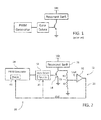
- the circuit 10 includes a low-side drive transistor 14 coupled to a load circuit 16.
- the low-side drive transistor 14 may comprise an insulated gate bi-polar transistor (IGBT) and the load circuit 16 may comprise a resonant tank circuit.
- the resonant tank circuit may, for example, comprise an inductance and capacitance coupled in parallel.
- a first terminal of the resonant tank circuit is coupled to a DC supply node configured to receive a DC supply voltage Vdc.
- a second terminal of the resonant tank circuit is coupled to a collector terminal of the IGBT 14.
- the emitter terminal of the IGBT 14 is coupled to a reference supply node (for example, ground).
- the gate terminal of the IGBT is driven by a drive signal output from a gate driver circuit 18.
- the gate driver circuit 18 may, for example, comprise a totem pole push-pull driver circuit as known in the art.
- the gate driver circuit 18 is actuated by a pulse width modulation (PWM) control signal generated by a PWM generator circuit 24.
- PWM pulse width modulation
- the gate driver circuit 18 further includes a force on circuit 20 that is configured, when actuated by the assertion of an over-voltage control (OVC) signal on feedback line 22, to cause the gate driver circuit 18 to output a drive signal that forces the IGBT 14 to turn on irrespective of the PWM control signal.
- OFC over-voltage control
- the over-voltage protection circuit 12 includes a resistive divider circuit formed by series connected resistors R1 and R2 and configured to function as a voltage sensor. One terminal of the resistive divider circuit is coupled to the collector terminal of the IGBT 14. The other terminal of the resistive divider circuit is coupled to the reference supply node. Thus, the voltage drop across the resistive divider circuit is equal to (or at least representative of) the voltage drop across the collector and emitter terminals of the IGBT 14 (i.e., the voltage drop equals Vce).
- the resistive divider circuit includes a tap node 30 at the series connection point of the resistors R1 and R2.
- the voltage at tap node 30 is a fraction of the voltage Vce, wherein that fraction is set by the resistance values of the resistors R1 and R2.
- the voltage V30 is applied to the noninverting input terminal of a comparator circuit 32.
- the inverting input terminal of the comparator 32 receives a reference voltage Vref.
- the comparator circuit 32 compares the voltage V30 to the voltage Vref and generates the OVC signal on line 22 having a logic state responsive to the comparison. In particular, the OVC signal transitions to logic high (i.e., is asserted) when the voltage V30 exceeds the voltage Vref.
- the comparator circuit 32 is a hysteresis comparator, so the comparison of voltage V30 and Vref leading the state changes for the OVC signal is subject to a built-in hysteresis.
- the force on circuit 20 operates responsive to assertion of the OVC signal. When the OVC signal is logic high, the force on circuit 20 causes the gate driver circuit 18 to force the drive signal to a logic high state (and thus turn on the IGBT 14) regardless of the state of the received PWM signal.
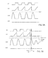
- the first waveform shows the drive signal (DS) applied to the control terminal of the IGBT 14.
- the IGBT 14 is turned on when the drive signal DS is logic high.
- the current flowing through the IGBT 14 (referenced as I14) will ramp up until the IGBT 14 is turned off when the drive signal DS transitions to logic low. At that point, the voltage across the collector to emitter terminals rises and then falls in accordance with the resonance characteristics of the load circuit 16.
- FIG. 3B showing operating waveforms for the low-side drive circuit 10 in the presence of an over-voltage condition.
- the waveforms of Figure 3B are similar to those of Figure 3A except that at time tovc, the voltage across the collector to emitter terminals rises to experience an over-voltage condition.
- the over-voltage condition may arise due to a transient spike on the voltage Vdc, or perhaps due to an increase in the voltage Vdc. This is represented by the voltage V30 exceeding the reference voltage Vref.
- time td the OVC signal at the output of the comparator circuit 32 changes state (i.e., transitions to logic high).
- the force on circuit 20 is responsive to the assertion of the OVC signal and forces the gate driver circuit 18 to output a logic high state for the drive signal DS (even though the PWM signal is logic low). This causes the IGBT 14 to turn on and current increases through the IGBT 14.
- the over-voltage condition is suppressed as the voltage V30 is shown to fall back below the reference voltage Vref in response to the IGBT 14 turning on. Thus occurs prior to the over-voltage rising to exceed either the essential margin set as a function of propagation delay or the maximum limit of the transistor device.
- the output of the comparator circuit 32 transitions the OVC signal back to logic low (at time tf) and the force on circuit 20 is deactuated.
- the gate driver circuit 18 is thereafter once again responsive to the PWM signal.
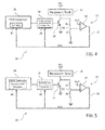
- the PWM generator 24 includes disable circuitry 40 configured to disable operation of the PWM generator (i.e., terminate output of the PWM signal) in response to the logic high state of the OVC signal.
- the PWM signal remains logic low after time tovc, and the drive signal DS remains logic low after the OVC signal transitions back to logic low.
- the IGBT 14 is no longer actuated and the voltage across the collector to emitter terminals is left to ring out in accordance with the resonance characteristics of the load circuit 16.
- the PWM generator 24 includes soft-start circuitry 42 configured to implement a soft-start mode of operation for the PWM generator in response to the logic high state of the OVC signal.
- the PWM signal is initially driven logic low at time tovc, and the drive signal DS transitions to logic low after the OVC signal transitions back to logic low.
- the IGBT 14 is turned off and the voltage across the collector to emitter terminals is left to ring out in accordance with the resonance characteristics of the load circuit 16.
- the PWM generator 24 is restarted with a reduced PWM duty cycle during start up.
- normal PWM drive operation proceeds (for example, like that present before time tovc).
- the PWM generator 24 includes excessive over-voltage condition detection circuitry 44 configured to modify the pulse width of the PWM signal output by the PWM generator in response to the number of incidents where the OVC signal has been asserted.
- the PWM signal is initially driven logic low at time tovc, and the drive signal DS remains logic low after the OVC signal transitions back to logic low.
- the IGBT 14 is turned off and the voltage across the collector to emitter terminals is left to ring out in accordance with the resonance characteristics of the load circuit 16.
- the PWM generator 24 is restarted with a reduced PWM duty cycle (for example, in soft-start mode as discussed above with respect to Figure 4 ).
- the duty cycle of the PWM signal during that normal operating mode is dependent on the number of times the OVC signal has previously been asserted logic high. If the number of times exceeds a first threshold (TH1), the PWM generator 24 will generate the PWM signal with a progressively reduced duty cycle. If the over-voltage condition persists and the number of times exceeds a second threshold (TH2>TH1), this is indicative of a persistent problem and operation of the PWM generator is disabled (for example, as discussed above with respect to Figure 3 ).
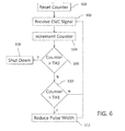
- the PWM generator 24 includes a counter configured to track the number of instances that the OVC signal is asserted. That counter is reset in step 100.
- the PWM generator waits for assertion of the OVC signal.
- the counter is incremented in step 104.
- a comparison of the count value stored in the counter is then made in step 106 against the second threshold (TH2). If the count value exceeds the second threshold, the PWM generator enters a shut down or disable mode of operation in step 108 wherein no PWM signal is generated.
- step 106 If the comparison in step 106 is not satisfied, the count value is instead compared against the first threshold (TH1) in step 110. If the count value exceeds the first threshold, the PWM generator incrementally reduces the pulse width (duty cycle) of the PWM signal in step 112. The process then returns to step 102 to waits for assertion of the next OVC signal. Upon receipt of the next OVC signal assertion, the comparison processes of steps 106 and 110 (if necessary) are repeated. With each pass through the comparison of step 110, the duty cycle of the PWM signal is progressively reduced. Eventually, in the presence of a persistent over-voltage condition (indicated when the second threshold is exceeded), the comparison of step 106 will be satisfied and a shut down in step 108 occurs.
- TH1 first threshold
- the PWM generator 24 is implemented, in one example, as integrated circuit device, such as a microcontroller.
- the excessive over-voltage condition detection circuitry 44 may then be implemented on the microcontroller as a mixture of hardware and software. Additionally, the functionalities for the disable circuitry 40 and the soft-start circuitry 42 may be supported by the microcontroller using hardware or a combination of hardware and software.
- the inductor of the resonant tank circuit 16 may comprise the heating coil for an induction heating/cooking system.
- a quasi-resonant single switch topology is implemented through the IGBT 14.
- a transient increase of the supply voltage Vdc can result in damage to the IGBT 14.
- the assertion of the OVC signal in response to that transient increase protects the IGBT 14 by forcing a turn on of the IGBT 14 and reducing the collector to emitter voltage Vce below the over-voltage threshold.
Landscapes
- Physics & Mathematics (AREA)
- Electromagnetism (AREA)
- Engineering & Computer Science (AREA)
- Power Engineering (AREA)
- Inverter Devices (AREA)
- Electronic Switches (AREA)
- Power Conversion In General (AREA)
- Dc-Dc Converters (AREA)
Applications Claiming Priority (1)
| Application Number | Priority Date | Filing Date | Title |
|---|---|---|---|
| US14/509,427 US9331474B1 (en) | 2014-10-08 | 2014-10-08 | Over-voltage protection circuit for a drive transistor |
Publications (2)
| Publication Number | Publication Date |
|---|---|
| EP3007360A1 true EP3007360A1 (fr) | 2016-04-13 |
| EP3007360B1 EP3007360B1 (fr) | 2021-01-20 |
Family
ID=54251396
Family Applications (1)
| Application Number | Title | Priority Date | Filing Date |
|---|---|---|---|
| EP15187680.2A Active EP3007360B1 (fr) | 2014-10-08 | 2015-09-30 | Circuit de protection contre les surtensions pour un transistor de pilotage |
Country Status (3)
| Country | Link |
|---|---|
| US (1) | US9331474B1 (fr) |
| EP (1) | EP3007360B1 (fr) |
| CN (3) | CN108988301B (fr) |
Families Citing this family (12)
| Publication number | Priority date | Publication date | Assignee | Title |
|---|---|---|---|---|
| US9331474B1 (en) * | 2014-10-08 | 2016-05-03 | Stmicroelectronics International N.V. | Over-voltage protection circuit for a drive transistor |
| US10018676B2 (en) * | 2014-11-06 | 2018-07-10 | Rockwell Automation Technologies, Inc. | Electromagnetic switch interlock system and method |
| CN204967246U (zh) * | 2015-09-25 | 2016-01-13 | 江森自控空调冷冻设备(无锡)有限公司 | Igbt短路检测保护电路及基于igbt的可控整流电路 |
| US10477626B2 (en) | 2016-11-23 | 2019-11-12 | Alpha And Omega Semiconductor (Cayman) Ltd. | Hard switching disable for switching power device |
| US10411692B2 (en) | 2016-11-23 | 2019-09-10 | Alpha And Omega Semiconductor Incorporated | Active clamp overvoltage protection for switching power device |
| US10476494B2 (en) | 2017-03-20 | 2019-11-12 | Alpha And Omega Semiconductor (Cayman) Ltd. | Intelligent power modules for resonant converters |
| US10110216B1 (en) * | 2017-06-30 | 2018-10-23 | Dialog Semiconductor (Uk) Limited | Over voltage protection of a transistor device |
| US10778082B2 (en) | 2018-06-08 | 2020-09-15 | Stmicroelectronics International N.V. | Control circuitry for increasing power output in quasi-resonant converters |
| US11678410B2 (en) * | 2019-07-24 | 2023-06-13 | Haier Us Appliance Solutions, Inc. | Determining presence of compatible cookware in induction heating systems |
| US11768000B2 (en) * | 2020-03-24 | 2023-09-26 | Johnson Controls Tyco IP Holdings LLP | System and method to operate HVAC system during voltage variation event |
| CN113162593B (zh) * | 2021-04-27 | 2022-11-04 | 杭州士兰微电子股份有限公司 | 晶体管的驱动系统 |
| CN116054094B (zh) * | 2023-01-19 | 2025-01-28 | 苏州纳芯微电子股份有限公司 | 一种用于igbt驱动的自适应vce过压保护电路 |
Citations (6)
| Publication number | Priority date | Publication date | Assignee | Title |
|---|---|---|---|---|
| GB2062985A (en) * | 1979-11-12 | 1981-05-28 | Matsushita Electric Industrial Co Ltd | Small load detection by comparison between input and output parameters of an induction heat cooking apparatus |
| US4890185A (en) * | 1987-12-23 | 1989-12-26 | Lenze Gmbh & Co. Kg Aerzen | Circuit for protecting a switching transistor |
| US7315439B2 (en) * | 2002-07-10 | 2008-01-01 | Eupec Europaeische Gesellschaft Fur Leistungshalbleiter Mbh | Method and circuit arrangement for limiting an overvoltage |
| US20120320476A1 (en) * | 2011-06-16 | 2012-12-20 | Disney Donald R | High-voltage devices with integrated over-voltage protection and associated methods |
| US20130277362A1 (en) * | 2012-04-19 | 2013-10-24 | International Rectifier Corporation | Power Converter with Over-Voltage Protection |
| EP2690923A1 (fr) * | 2012-07-23 | 2014-01-29 | Whirlpool Corporation | Dispositif dýalimentation électrique pour appareil électroménager et son procédé d'utilisation |
Family Cites Families (14)
| Publication number | Priority date | Publication date | Assignee | Title |
|---|---|---|---|---|
| US4371824A (en) * | 1979-07-05 | 1983-02-01 | Eaton Corporation | Base drive and overlap protection circuit |
| US7254000B1 (en) * | 2005-06-20 | 2007-08-07 | Nexem, Inc. | Over voltage protection scheme for synchronous buck converter |
| CN101295872B (zh) * | 2007-04-28 | 2010-04-14 | 昂宝电子(上海)有限公司 | 为功率转换器提供过电流和过功率保护的系统和方法 |
| JP4748356B2 (ja) | 2005-10-13 | 2011-08-17 | サンケン電気株式会社 | 誘導加熱装置 |
| US7304464B2 (en) * | 2006-03-15 | 2007-12-04 | Micrel, Inc. | Switching voltage regulator with low current trickle mode |
| US7821750B2 (en) * | 2006-08-30 | 2010-10-26 | Leadtrend Technology Corp. | Voltage converter for preventing switch device from being damaged by voltage spike by utilizing protection circuit |
| CN201178498Y (zh) * | 2008-04-03 | 2009-01-07 | 深圳和而泰智能控制股份有限公司 | 电磁炉浪涌保护电路 |
| KR101643762B1 (ko) * | 2009-10-29 | 2016-08-11 | 페어차일드코리아반도체 주식회사 | 역률 보상 회로 및 역률보상 회로의 구동 방법 |
| US8487705B2 (en) * | 2010-05-26 | 2013-07-16 | Triquint Semiconductor, Inc. | Protection circuit for radio frequency power amplifier |
| CN101916985B (zh) * | 2010-07-20 | 2013-10-09 | 美的集团股份有限公司 | 一种igbt集电极过压双重保护的监控方法 |
| TW201240257A (en) * | 2011-03-17 | 2012-10-01 | Green Solution Tech Co Ltd | Transistor circuit with protecting function |
| US8982521B2 (en) * | 2013-01-21 | 2015-03-17 | Shenzhen China Star | Overvoltage protection method for backlight driver |
| CN203166499U (zh) * | 2013-03-25 | 2013-08-28 | 长沙理工大学 | 电磁炉的igbt过压保护电路 |
| US9331474B1 (en) * | 2014-10-08 | 2016-05-03 | Stmicroelectronics International N.V. | Over-voltage protection circuit for a drive transistor |
-
2014
- 2014-10-08 US US14/509,427 patent/US9331474B1/en active Active
-
2015
- 2015-09-24 CN CN201810763090.8A patent/CN108988301B/zh active Active
- 2015-09-24 CN CN201510615928.5A patent/CN105514943B/zh active Active
- 2015-09-24 CN CN201520747630.5U patent/CN205004739U/zh not_active Expired - Fee Related
- 2015-09-30 EP EP15187680.2A patent/EP3007360B1/fr active Active
Patent Citations (6)
| Publication number | Priority date | Publication date | Assignee | Title |
|---|---|---|---|---|
| GB2062985A (en) * | 1979-11-12 | 1981-05-28 | Matsushita Electric Industrial Co Ltd | Small load detection by comparison between input and output parameters of an induction heat cooking apparatus |
| US4890185A (en) * | 1987-12-23 | 1989-12-26 | Lenze Gmbh & Co. Kg Aerzen | Circuit for protecting a switching transistor |
| US7315439B2 (en) * | 2002-07-10 | 2008-01-01 | Eupec Europaeische Gesellschaft Fur Leistungshalbleiter Mbh | Method and circuit arrangement for limiting an overvoltage |
| US20120320476A1 (en) * | 2011-06-16 | 2012-12-20 | Disney Donald R | High-voltage devices with integrated over-voltage protection and associated methods |
| US20130277362A1 (en) * | 2012-04-19 | 2013-10-24 | International Rectifier Corporation | Power Converter with Over-Voltage Protection |
| EP2690923A1 (fr) * | 2012-07-23 | 2014-01-29 | Whirlpool Corporation | Dispositif dýalimentation électrique pour appareil électroménager et son procédé d'utilisation |
Also Published As
| Publication number | Publication date |
|---|---|
| CN108988301A (zh) | 2018-12-11 |
| US20160105017A1 (en) | 2016-04-14 |
| CN108988301B (zh) | 2020-08-18 |
| EP3007360B1 (fr) | 2021-01-20 |
| CN205004739U (zh) | 2016-01-27 |
| US9331474B1 (en) | 2016-05-03 |
| CN105514943A (zh) | 2016-04-20 |
| CN105514943B (zh) | 2018-08-14 |
Similar Documents
| Publication | Publication Date | Title |
|---|---|---|
| US9331474B1 (en) | Over-voltage protection circuit for a drive transistor | |
| US10411692B2 (en) | Active clamp overvoltage protection for switching power device | |
| CN105577153B (zh) | 半导体装置 | |
| TWI448029B (zh) | A system and method for protecting a power conversion system under open circuit and / or short circuit conditions | |
| US9385617B2 (en) | Overcurrent protection circuit for a switching power supply apparatus | |
| US11271559B2 (en) | Intelligent power module control method for resonant converter | |
| US11159009B2 (en) | Voltage regulator over-current protection | |
| US8680837B2 (en) | Driver for driving power switch element | |
| US20130155560A1 (en) | Semiconductor Device | |
| US20180145676A1 (en) | Hard switching disable for switching power device | |
| TWI501519B (zh) | System controller and method for protecting and adjusting the power conversion system | |
| US9755508B2 (en) | Startup circuit and power supply circuit | |
| CN109462323B (zh) | 一种耦合到可以流通负载电流的负载上的功率半导体器件 | |
| US20120176827A1 (en) | Controller for secondary side control of a switch, power converter, and related synchronous rectification control method | |
| CN109428484A (zh) | 电源转换电路 | |
| CN114303309B (zh) | 过流保护电路及开关电路 | |
| CN112534668A (zh) | 升压转换器短路保护 | |
| US10120429B2 (en) | Current control circuit and a method therefor | |
| JP2013255304A (ja) | 異常検出装置 | |
| US10447027B1 (en) | Method and apparatus for reverse over current protection | |
| WO2018134839A1 (fr) | Régulateur de courant autopiloté |
Legal Events
| Date | Code | Title | Description |
|---|---|---|---|
| PUAI | Public reference made under article 153(3) epc to a published international application that has entered the european phase |
Free format text: ORIGINAL CODE: 0009012 |
|
| AK | Designated contracting states |
Kind code of ref document: A1 Designated state(s): AL AT BE BG CH CY CZ DE DK EE ES FI FR GB GR HR HU IE IS IT LI LT LU LV MC MK MT NL NO PL PT RO RS SE SI SK SM TR |
|
| AX | Request for extension of the european patent |
Extension state: BA ME |
|
| 17P | Request for examination filed |
Effective date: 20161006 |
|
| RBV | Designated contracting states (corrected) |
Designated state(s): AL AT BE BG CH CY CZ DE DK EE ES FI FR GB GR HR HU IE IS IT LI LT LU LV MC MK MT NL NO PL PT RO RS SE SI SK SM TR |
|
| STAA | Information on the status of an ep patent application or granted ep patent |
Free format text: STATUS: EXAMINATION IS IN PROGRESS |
|
| 17Q | First examination report despatched |
Effective date: 20171009 |
|
| GRAP | Despatch of communication of intention to grant a patent |
Free format text: ORIGINAL CODE: EPIDOSNIGR1 |
|
| STAA | Information on the status of an ep patent application or granted ep patent |
Free format text: STATUS: GRANT OF PATENT IS INTENDED |
|
| INTG | Intention to grant announced |
Effective date: 20200313 |
|
| GRAJ | Information related to disapproval of communication of intention to grant by the applicant or resumption of examination proceedings by the epo deleted |
Free format text: ORIGINAL CODE: EPIDOSDIGR1 |
|
| GRAL | Information related to payment of fee for publishing/printing deleted |
Free format text: ORIGINAL CODE: EPIDOSDIGR3 |
|
| GRAS | Grant fee paid |
Free format text: ORIGINAL CODE: EPIDOSNIGR3 |
|
| STAA | Information on the status of an ep patent application or granted ep patent |
Free format text: STATUS: EXAMINATION IS IN PROGRESS |
|
| INTC | Intention to grant announced (deleted) | ||
| GRAP | Despatch of communication of intention to grant a patent |
Free format text: ORIGINAL CODE: EPIDOSNIGR1 |
|
| STAA | Information on the status of an ep patent application or granted ep patent |
Free format text: STATUS: GRANT OF PATENT IS INTENDED |
|
| INTG | Intention to grant announced |
Effective date: 20200903 |
|
| RIN1 | Information on inventor provided before grant (corrected) |
Inventor name: MALLIK, RANAJAY Inventor name: JAIN, AKSHAT Inventor name: CATALISANO, GIUSEPPE Inventor name: ABBATELLI, LUIGI |
|
| GRAA | (expected) grant |
Free format text: ORIGINAL CODE: 0009210 |
|
| STAA | Information on the status of an ep patent application or granted ep patent |
Free format text: STATUS: THE PATENT HAS BEEN GRANTED |
|
| AK | Designated contracting states |
Kind code of ref document: B1 Designated state(s): AL AT BE BG CH CY CZ DE DK EE ES FI FR GB GR HR HU IE IS IT LI LT LU LV MC MK MT NL NO PL PT RO RS SE SI SK SM TR |
|
| REG | Reference to a national code |
Ref country code: GB Ref legal event code: FG4D |
|
| REG | Reference to a national code |
Ref country code: CH Ref legal event code: EP |
|
| REG | Reference to a national code |
Ref country code: DE Ref legal event code: R096 Ref document number: 602015064907 Country of ref document: DE |
|
| REG | Reference to a national code |
Ref country code: AT Ref legal event code: REF Ref document number: 1357233 Country of ref document: AT Kind code of ref document: T Effective date: 20210215 |
|
| REG | Reference to a national code |
Ref country code: IE Ref legal event code: FG4D |
|
| REG | Reference to a national code |
Ref country code: NL Ref legal event code: MP Effective date: 20210120 |
|
| REG | Reference to a national code |
Ref country code: LT Ref legal event code: MG9D |
|
| REG | Reference to a national code |
Ref country code: AT Ref legal event code: MK05 Ref document number: 1357233 Country of ref document: AT Kind code of ref document: T Effective date: 20210120 |
|
| PG25 | Lapsed in a contracting state [announced via postgrant information from national office to epo] |
Ref country code: PT Free format text: LAPSE BECAUSE OF FAILURE TO SUBMIT A TRANSLATION OF THE DESCRIPTION OR TO PAY THE FEE WITHIN THE PRESCRIBED TIME-LIMIT Effective date: 20210520 Ref country code: LT Free format text: LAPSE BECAUSE OF FAILURE TO SUBMIT A TRANSLATION OF THE DESCRIPTION OR TO PAY THE FEE WITHIN THE PRESCRIBED TIME-LIMIT Effective date: 20210120 Ref country code: GR Free format text: LAPSE BECAUSE OF FAILURE TO SUBMIT A TRANSLATION OF THE DESCRIPTION OR TO PAY THE FEE WITHIN THE PRESCRIBED TIME-LIMIT Effective date: 20210421 Ref country code: FI Free format text: LAPSE BECAUSE OF FAILURE TO SUBMIT A TRANSLATION OF THE DESCRIPTION OR TO PAY THE FEE WITHIN THE PRESCRIBED TIME-LIMIT Effective date: 20210120 Ref country code: HR Free format text: LAPSE BECAUSE OF FAILURE TO SUBMIT A TRANSLATION OF THE DESCRIPTION OR TO PAY THE FEE WITHIN THE PRESCRIBED TIME-LIMIT Effective date: 20210120 Ref country code: BG Free format text: LAPSE BECAUSE OF FAILURE TO SUBMIT A TRANSLATION OF THE DESCRIPTION OR TO PAY THE FEE WITHIN THE PRESCRIBED TIME-LIMIT Effective date: 20210420 Ref country code: NL Free format text: LAPSE BECAUSE OF FAILURE TO SUBMIT A TRANSLATION OF THE DESCRIPTION OR TO PAY THE FEE WITHIN THE PRESCRIBED TIME-LIMIT Effective date: 20210120 Ref country code: NO Free format text: LAPSE BECAUSE OF FAILURE TO SUBMIT A TRANSLATION OF THE DESCRIPTION OR TO PAY THE FEE WITHIN THE PRESCRIBED TIME-LIMIT Effective date: 20210420 |
|
| PG25 | Lapsed in a contracting state [announced via postgrant information from national office to epo] |
Ref country code: LV Free format text: LAPSE BECAUSE OF FAILURE TO SUBMIT A TRANSLATION OF THE DESCRIPTION OR TO PAY THE FEE WITHIN THE PRESCRIBED TIME-LIMIT Effective date: 20210120 Ref country code: PL Free format text: LAPSE BECAUSE OF FAILURE TO SUBMIT A TRANSLATION OF THE DESCRIPTION OR TO PAY THE FEE WITHIN THE PRESCRIBED TIME-LIMIT Effective date: 20210120 Ref country code: RS Free format text: LAPSE BECAUSE OF FAILURE TO SUBMIT A TRANSLATION OF THE DESCRIPTION OR TO PAY THE FEE WITHIN THE PRESCRIBED TIME-LIMIT Effective date: 20210120 Ref country code: AT Free format text: LAPSE BECAUSE OF FAILURE TO SUBMIT A TRANSLATION OF THE DESCRIPTION OR TO PAY THE FEE WITHIN THE PRESCRIBED TIME-LIMIT Effective date: 20210120 Ref country code: SE Free format text: LAPSE BECAUSE OF FAILURE TO SUBMIT A TRANSLATION OF THE DESCRIPTION OR TO PAY THE FEE WITHIN THE PRESCRIBED TIME-LIMIT Effective date: 20210120 |
|
| PG25 | Lapsed in a contracting state [announced via postgrant information from national office to epo] |
Ref country code: IS Free format text: LAPSE BECAUSE OF FAILURE TO SUBMIT A TRANSLATION OF THE DESCRIPTION OR TO PAY THE FEE WITHIN THE PRESCRIBED TIME-LIMIT Effective date: 20210520 |
|
| REG | Reference to a national code |
Ref country code: DE Ref legal event code: R097 Ref document number: 602015064907 Country of ref document: DE |
|
| PG25 | Lapsed in a contracting state [announced via postgrant information from national office to epo] |
Ref country code: EE Free format text: LAPSE BECAUSE OF FAILURE TO SUBMIT A TRANSLATION OF THE DESCRIPTION OR TO PAY THE FEE WITHIN THE PRESCRIBED TIME-LIMIT Effective date: 20210120 Ref country code: CZ Free format text: LAPSE BECAUSE OF FAILURE TO SUBMIT A TRANSLATION OF THE DESCRIPTION OR TO PAY THE FEE WITHIN THE PRESCRIBED TIME-LIMIT Effective date: 20210120 Ref country code: SM Free format text: LAPSE BECAUSE OF FAILURE TO SUBMIT A TRANSLATION OF THE DESCRIPTION OR TO PAY THE FEE WITHIN THE PRESCRIBED TIME-LIMIT Effective date: 20210120 |
|
| PLBE | No opposition filed within time limit |
Free format text: ORIGINAL CODE: 0009261 |
|
| STAA | Information on the status of an ep patent application or granted ep patent |
Free format text: STATUS: NO OPPOSITION FILED WITHIN TIME LIMIT |
|
| PG25 | Lapsed in a contracting state [announced via postgrant information from national office to epo] |
Ref country code: DK Free format text: LAPSE BECAUSE OF FAILURE TO SUBMIT A TRANSLATION OF THE DESCRIPTION OR TO PAY THE FEE WITHIN THE PRESCRIBED TIME-LIMIT Effective date: 20210120 Ref country code: ES Free format text: LAPSE BECAUSE OF FAILURE TO SUBMIT A TRANSLATION OF THE DESCRIPTION OR TO PAY THE FEE WITHIN THE PRESCRIBED TIME-LIMIT Effective date: 20210120 Ref country code: SK Free format text: LAPSE BECAUSE OF FAILURE TO SUBMIT A TRANSLATION OF THE DESCRIPTION OR TO PAY THE FEE WITHIN THE PRESCRIBED TIME-LIMIT Effective date: 20210120 Ref country code: RO Free format text: LAPSE BECAUSE OF FAILURE TO SUBMIT A TRANSLATION OF THE DESCRIPTION OR TO PAY THE FEE WITHIN THE PRESCRIBED TIME-LIMIT Effective date: 20210120 |
|
| 26N | No opposition filed |
Effective date: 20211021 |
|
| PG25 | Lapsed in a contracting state [announced via postgrant information from national office to epo] |
Ref country code: AL Free format text: LAPSE BECAUSE OF FAILURE TO SUBMIT A TRANSLATION OF THE DESCRIPTION OR TO PAY THE FEE WITHIN THE PRESCRIBED TIME-LIMIT Effective date: 20210120 |
|
| PG25 | Lapsed in a contracting state [announced via postgrant information from national office to epo] |
Ref country code: SI Free format text: LAPSE BECAUSE OF FAILURE TO SUBMIT A TRANSLATION OF THE DESCRIPTION OR TO PAY THE FEE WITHIN THE PRESCRIBED TIME-LIMIT Effective date: 20210120 |
|
| PG25 | Lapsed in a contracting state [announced via postgrant information from national office to epo] |
Ref country code: IT Free format text: LAPSE BECAUSE OF FAILURE TO SUBMIT A TRANSLATION OF THE DESCRIPTION OR TO PAY THE FEE WITHIN THE PRESCRIBED TIME-LIMIT Effective date: 20210120 |
|
| REG | Reference to a national code |
Ref country code: CH Ref legal event code: PL |
|
| REG | Reference to a national code |
Ref country code: BE Ref legal event code: MM Effective date: 20210930 |
|
| GBPC | Gb: european patent ceased through non-payment of renewal fee |
Effective date: 20210930 |
|
| PG25 | Lapsed in a contracting state [announced via postgrant information from national office to epo] |
Ref country code: IS Free format text: LAPSE BECAUSE OF FAILURE TO SUBMIT A TRANSLATION OF THE DESCRIPTION OR TO PAY THE FEE WITHIN THE PRESCRIBED TIME-LIMIT Effective date: 20210520 Ref country code: MC Free format text: LAPSE BECAUSE OF FAILURE TO SUBMIT A TRANSLATION OF THE DESCRIPTION OR TO PAY THE FEE WITHIN THE PRESCRIBED TIME-LIMIT Effective date: 20210120 |
|
| PG25 | Lapsed in a contracting state [announced via postgrant information from national office to epo] |
Ref country code: LU Free format text: LAPSE BECAUSE OF NON-PAYMENT OF DUE FEES Effective date: 20210930 Ref country code: IE Free format text: LAPSE BECAUSE OF NON-PAYMENT OF DUE FEES Effective date: 20210930 Ref country code: GB Free format text: LAPSE BECAUSE OF NON-PAYMENT OF DUE FEES Effective date: 20210930 Ref country code: FR Free format text: LAPSE BECAUSE OF NON-PAYMENT OF DUE FEES Effective date: 20210930 Ref country code: BE Free format text: LAPSE BECAUSE OF NON-PAYMENT OF DUE FEES Effective date: 20210930 |
|
| PG25 | Lapsed in a contracting state [announced via postgrant information from national office to epo] |
Ref country code: LI Free format text: LAPSE BECAUSE OF NON-PAYMENT OF DUE FEES Effective date: 20210930 Ref country code: CH Free format text: LAPSE BECAUSE OF NON-PAYMENT OF DUE FEES Effective date: 20210930 |
|
| REG | Reference to a national code |
Ref country code: DE Ref legal event code: R081 Ref document number: 602015064907 Country of ref document: DE Owner name: STMICROELECTRONICS INTERNATIONAL N.V., PLAN-LE, CH Free format text: FORMER OWNERS: STMICROELECTRONICS INTERNATIONAL N.V., AMSTERDAM, NL; STMICROELECTRONICS S.R.L., AGRATE BRIANZA, IT |
|
| PG25 | Lapsed in a contracting state [announced via postgrant information from national office to epo] |
Ref country code: HU Free format text: LAPSE BECAUSE OF FAILURE TO SUBMIT A TRANSLATION OF THE DESCRIPTION OR TO PAY THE FEE WITHIN THE PRESCRIBED TIME-LIMIT; INVALID AB INITIO Effective date: 20150930 |
|
| PG25 | Lapsed in a contracting state [announced via postgrant information from national office to epo] |
Ref country code: CY Free format text: LAPSE BECAUSE OF FAILURE TO SUBMIT A TRANSLATION OF THE DESCRIPTION OR TO PAY THE FEE WITHIN THE PRESCRIBED TIME-LIMIT Effective date: 20210120 |
|
| PG25 | Lapsed in a contracting state [announced via postgrant information from national office to epo] |
Ref country code: MK Free format text: LAPSE BECAUSE OF FAILURE TO SUBMIT A TRANSLATION OF THE DESCRIPTION OR TO PAY THE FEE WITHIN THE PRESCRIBED TIME-LIMIT Effective date: 20210120 |
|
| PG25 | Lapsed in a contracting state [announced via postgrant information from national office to epo] |
Ref country code: TR Free format text: LAPSE BECAUSE OF FAILURE TO SUBMIT A TRANSLATION OF THE DESCRIPTION OR TO PAY THE FEE WITHIN THE PRESCRIBED TIME-LIMIT Effective date: 20210120 |
|
| PG25 | Lapsed in a contracting state [announced via postgrant information from national office to epo] |
Ref country code: MT Free format text: LAPSE BECAUSE OF FAILURE TO SUBMIT A TRANSLATION OF THE DESCRIPTION OR TO PAY THE FEE WITHIN THE PRESCRIBED TIME-LIMIT Effective date: 20210120 |
|
| PGFP | Annual fee paid to national office [announced via postgrant information from national office to epo] |
Ref country code: DE Payment date: 20250820 Year of fee payment: 11 |
|
| REG | Reference to a national code |
Ref country code: DE Ref legal event code: R082 Ref document number: 602015064907 Country of ref document: DE Representative=s name: WESTPHAL, MUSSGNUG & PARTNER PATENTANWAELTE MI, DE |