EP3010064B1 - Composé de transfert de charge dans l'espace et diode électroluminescente organique et dispositif d'affichage utilisant celui-ci - Google Patents
Composé de transfert de charge dans l'espace et diode électroluminescente organique et dispositif d'affichage utilisant celui-ci Download PDFInfo
- Publication number
- EP3010064B1 EP3010064B1 EP15188932.6A EP15188932A EP3010064B1 EP 3010064 B1 EP3010064 B1 EP 3010064B1 EP 15188932 A EP15188932 A EP 15188932A EP 3010064 B1 EP3010064 B1 EP 3010064B1
- Authority
- EP
- European Patent Office
- Prior art keywords
- compound
- equivalent
- mixture
- charge transfer
- space
- Prior art date
- Legal status (The legal status is an assumption and is not a legal conclusion. Google has not performed a legal analysis and makes no representation as to the accuracy of the status listed.)
- Active
Links
- 0 *c(cc1)ccc1-c1cccc2c1c(-c(cc1)ccc1O)ccc2 Chemical compound *c(cc1)ccc1-c1cccc2c1c(-c(cc1)ccc1O)ccc2 0.000 description 13
- SWJPEBQEEAHIGZ-UHFFFAOYSA-N Brc(cc1)ccc1Br Chemical compound Brc(cc1)ccc1Br SWJPEBQEEAHIGZ-UHFFFAOYSA-N 0.000 description 3
- NBPVDUKMHKDRPR-UHFFFAOYSA-N Brc(cc1)ccc1-c(cc1)cc2c1[nH]c1ccccc21 Chemical compound Brc(cc1)ccc1-c(cc1)cc2c1[nH]c1ccccc21 NBPVDUKMHKDRPR-UHFFFAOYSA-N 0.000 description 2
- JEYLGFCAZBGCMC-UHFFFAOYSA-N Brc(cc1)ccc1-c(cc1)cc(c2ccccc22)c1[n]2-c1ccccc1 Chemical compound Brc(cc1)ccc1-c(cc1)cc(c2ccccc22)c1[n]2-c1ccccc1 JEYLGFCAZBGCMC-UHFFFAOYSA-N 0.000 description 1
- FCHUOBPHXDXZBK-UHFFFAOYSA-N Brc(cc1)ccc1-c1cccnc1 Chemical compound Brc(cc1)ccc1-c1cccnc1 FCHUOBPHXDXZBK-UHFFFAOYSA-N 0.000 description 1
- GJBAOBLGEYEVMJ-UHFFFAOYSA-N Brc(cc1)ccc1-c1cncnc1 Chemical compound Brc(cc1)ccc1-c1cncnc1 GJBAOBLGEYEVMJ-UHFFFAOYSA-N 0.000 description 1
- PEYQCEFPKMIOFP-UHFFFAOYSA-N CC1(C)OB(c(cc2)ccc2-c2nc3ccccc3[n]2-c2ccccc2)OC1(C)C Chemical compound CC1(C)OB(c(cc2)ccc2-c2nc3ccccc3[n]2-c2ccccc2)OC1(C)C PEYQCEFPKMIOFP-UHFFFAOYSA-N 0.000 description 1
- MGKPDVRJFZOSFV-UHFFFAOYSA-N Cc1nc(cccc2)c2[n]1-c1ccccc1 Chemical compound Cc1nc(cccc2)c2[n]1-c1ccccc1 MGKPDVRJFZOSFV-UHFFFAOYSA-N 0.000 description 1
- QILPWYYRSLAATK-UHFFFAOYSA-N c(cc1)cc(c2ccccc22)c1[n]2-c(cc1)ccc1-c1ccc(ccc(-c(cc2)ccc2-c2ccncc2)c2)c2c1 Chemical compound c(cc1)cc(c2ccccc22)c1[n]2-c(cc1)ccc1-c1ccc(ccc(-c(cc2)ccc2-c2ccncc2)c2)c2c1 QILPWYYRSLAATK-UHFFFAOYSA-N 0.000 description 1
- YJUXXUHHCBXQPH-UHFFFAOYSA-N c(cc1)ccc1-[n]1c(-c(cc2)ccc2-c2cccc3cccc(-c(cc4)ccc4-[n]4c5ccccc5c5c4cccc5)c23)nc2c1cccc2 Chemical compound c(cc1)ccc1-[n]1c(-c(cc2)ccc2-c2cccc3cccc(-c(cc4)ccc4-[n]4c5ccccc5c5c4cccc5)c23)nc2c1cccc2 YJUXXUHHCBXQPH-UHFFFAOYSA-N 0.000 description 1
- IXSDZRIFOSVZQA-UHFFFAOYSA-N c(cc1)ccc1-[n]1c(ccc(-c(cc2)ccc2-c2c3c(-c(cc4)ccc4-c4ccncn4)cccc3ccc2)c2)c2c2ccccc12 Chemical compound c(cc1)ccc1-[n]1c(ccc(-c(cc2)ccc2-c2c3c(-c(cc4)ccc4-c4ccncn4)cccc3ccc2)c2)c2c2ccccc12 IXSDZRIFOSVZQA-UHFFFAOYSA-N 0.000 description 1
Images


Classifications
-
- H—ELECTRICITY
- H10—SEMICONDUCTOR DEVICES; ELECTRIC SOLID-STATE DEVICES NOT OTHERWISE PROVIDED FOR
- H10K—ORGANIC ELECTRIC SOLID-STATE DEVICES
- H10K85/00—Organic materials used in the body or electrodes of devices covered by this subclass
- H10K85/60—Organic compounds having low molecular weight
- H10K85/615—Polycyclic condensed aromatic hydrocarbons, e.g. anthracene
- H10K85/626—Polycyclic condensed aromatic hydrocarbons, e.g. anthracene containing more than one polycyclic condensed aromatic rings, e.g. bis-anthracene
-
- C—CHEMISTRY; METALLURGY
- C09—DYES; PAINTS; POLISHES; NATURAL RESINS; ADHESIVES; COMPOSITIONS NOT OTHERWISE PROVIDED FOR; APPLICATIONS OF MATERIALS NOT OTHERWISE PROVIDED FOR
- C09K—MATERIALS FOR MISCELLANEOUS APPLICATIONS, NOT PROVIDED FOR ELSEWHERE
- C09K11/00—Luminescent materials, e.g. electroluminescent or chemiluminescent
- C09K11/06—Luminescent materials, e.g. electroluminescent or chemiluminescent containing organic luminescent materials
-
- C—CHEMISTRY; METALLURGY
- C07—ORGANIC CHEMISTRY
- C07D—HETEROCYCLIC COMPOUNDS
- C07D213/00—Heterocyclic compounds containing six-membered rings, not condensed with other rings, with one nitrogen atom as the only ring hetero atom and three or more double bonds between ring members or between ring members and non-ring members
- C07D213/02—Heterocyclic compounds containing six-membered rings, not condensed with other rings, with one nitrogen atom as the only ring hetero atom and three or more double bonds between ring members or between ring members and non-ring members having three double bonds between ring members or between ring members and non-ring members
- C07D213/04—Heterocyclic compounds containing six-membered rings, not condensed with other rings, with one nitrogen atom as the only ring hetero atom and three or more double bonds between ring members or between ring members and non-ring members having three double bonds between ring members or between ring members and non-ring members having no bond between the ring nitrogen atom and a non-ring member or having only hydrogen or carbon atoms directly attached to the ring nitrogen atom
- C07D213/24—Heterocyclic compounds containing six-membered rings, not condensed with other rings, with one nitrogen atom as the only ring hetero atom and three or more double bonds between ring members or between ring members and non-ring members having three double bonds between ring members or between ring members and non-ring members having no bond between the ring nitrogen atom and a non-ring member or having only hydrogen or carbon atoms directly attached to the ring nitrogen atom with substituted hydrocarbon radicals attached to ring carbon atoms
- C07D213/36—Radicals substituted by singly-bound nitrogen atoms
- C07D213/38—Radicals substituted by singly-bound nitrogen atoms having only hydrogen or hydrocarbon radicals attached to the substituent nitrogen atom
-
- C—CHEMISTRY; METALLURGY
- C07—ORGANIC CHEMISTRY
- C07D—HETEROCYCLIC COMPOUNDS
- C07D235/00—Heterocyclic compounds containing 1,3-diazole or hydrogenated 1,3-diazole rings, condensed with other rings
- C07D235/02—Heterocyclic compounds containing 1,3-diazole or hydrogenated 1,3-diazole rings, condensed with other rings condensed with carbocyclic rings or ring systems
- C07D235/04—Benzimidazoles; Hydrogenated benzimidazoles
- C07D235/18—Benzimidazoles; Hydrogenated benzimidazoles with aryl radicals directly attached in position 2
-
- C—CHEMISTRY; METALLURGY
- C07—ORGANIC CHEMISTRY
- C07D—HETEROCYCLIC COMPOUNDS
- C07D401/00—Heterocyclic compounds containing two or more hetero rings, having nitrogen atoms as the only ring hetero atoms, at least one ring being a six-membered ring with only one nitrogen atom
- C07D401/02—Heterocyclic compounds containing two or more hetero rings, having nitrogen atoms as the only ring hetero atoms, at least one ring being a six-membered ring with only one nitrogen atom containing two hetero rings
- C07D401/10—Heterocyclic compounds containing two or more hetero rings, having nitrogen atoms as the only ring hetero atoms, at least one ring being a six-membered ring with only one nitrogen atom containing two hetero rings linked by a carbon chain containing aromatic rings
-
- C—CHEMISTRY; METALLURGY
- C07—ORGANIC CHEMISTRY
- C07D—HETEROCYCLIC COMPOUNDS
- C07D403/00—Heterocyclic compounds containing two or more hetero rings, having nitrogen atoms as the only ring hetero atoms, not provided for by group C07D401/00
- C07D403/02—Heterocyclic compounds containing two or more hetero rings, having nitrogen atoms as the only ring hetero atoms, not provided for by group C07D401/00 containing two hetero rings
- C07D403/10—Heterocyclic compounds containing two or more hetero rings, having nitrogen atoms as the only ring hetero atoms, not provided for by group C07D401/00 containing two hetero rings linked by a carbon chain containing aromatic rings
-
- C—CHEMISTRY; METALLURGY
- C09—DYES; PAINTS; POLISHES; NATURAL RESINS; ADHESIVES; COMPOSITIONS NOT OTHERWISE PROVIDED FOR; APPLICATIONS OF MATERIALS NOT OTHERWISE PROVIDED FOR
- C09K—MATERIALS FOR MISCELLANEOUS APPLICATIONS, NOT PROVIDED FOR ELSEWHERE
- C09K11/00—Luminescent materials, e.g. electroluminescent or chemiluminescent
- C09K11/02—Use of particular materials as binders, particle coatings or suspension media therefor
- C09K11/025—Use of particular materials as binders, particle coatings or suspension media therefor non-luminescent particle coatings or suspension media
-
- H—ELECTRICITY
- H10—SEMICONDUCTOR DEVICES; ELECTRIC SOLID-STATE DEVICES NOT OTHERWISE PROVIDED FOR
- H10K—ORGANIC ELECTRIC SOLID-STATE DEVICES
- H10K50/00—Organic light-emitting devices
- H10K50/10—OLEDs or polymer light-emitting diodes [PLED]
- H10K50/11—OLEDs or polymer light-emitting diodes [PLED] characterised by the electroluminescent [EL] layers
-
- H—ELECTRICITY
- H10—SEMICONDUCTOR DEVICES; ELECTRIC SOLID-STATE DEVICES NOT OTHERWISE PROVIDED FOR
- H10K—ORGANIC ELECTRIC SOLID-STATE DEVICES
- H10K59/00—Integrated devices, or assemblies of multiple devices, comprising at least one organic light-emitting element covered by group H10K50/00
- H10K59/10—OLED displays
- H10K59/12—Active-matrix OLED [AMOLED] displays
- H10K59/124—Insulating layers formed between TFT elements and OLED elements
-
- H—ELECTRICITY
- H10—SEMICONDUCTOR DEVICES; ELECTRIC SOLID-STATE DEVICES NOT OTHERWISE PROVIDED FOR
- H10K—ORGANIC ELECTRIC SOLID-STATE DEVICES
- H10K85/00—Organic materials used in the body or electrodes of devices covered by this subclass
- H10K85/60—Organic compounds having low molecular weight
- H10K85/615—Polycyclic condensed aromatic hydrocarbons, e.g. anthracene
-
- H—ELECTRICITY
- H10—SEMICONDUCTOR DEVICES; ELECTRIC SOLID-STATE DEVICES NOT OTHERWISE PROVIDED FOR
- H10K—ORGANIC ELECTRIC SOLID-STATE DEVICES
- H10K85/00—Organic materials used in the body or electrodes of devices covered by this subclass
- H10K85/60—Organic compounds having low molecular weight
- H10K85/631—Amine compounds having at least two aryl rest on at least one amine-nitrogen atom, e.g. triphenylamine
- H10K85/633—Amine compounds having at least two aryl rest on at least one amine-nitrogen atom, e.g. triphenylamine comprising polycyclic condensed aromatic hydrocarbons as substituents on the nitrogen atom
-
- H—ELECTRICITY
- H10—SEMICONDUCTOR DEVICES; ELECTRIC SOLID-STATE DEVICES NOT OTHERWISE PROVIDED FOR
- H10K—ORGANIC ELECTRIC SOLID-STATE DEVICES
- H10K85/00—Organic materials used in the body or electrodes of devices covered by this subclass
- H10K85/60—Organic compounds having low molecular weight
- H10K85/631—Amine compounds having at least two aryl rest on at least one amine-nitrogen atom, e.g. triphenylamine
- H10K85/636—Amine compounds having at least two aryl rest on at least one amine-nitrogen atom, e.g. triphenylamine comprising heteroaromatic hydrocarbons as substituents on the nitrogen atom
-
- H—ELECTRICITY
- H10—SEMICONDUCTOR DEVICES; ELECTRIC SOLID-STATE DEVICES NOT OTHERWISE PROVIDED FOR
- H10K—ORGANIC ELECTRIC SOLID-STATE DEVICES
- H10K85/00—Organic materials used in the body or electrodes of devices covered by this subclass
- H10K85/60—Organic compounds having low molecular weight
- H10K85/649—Aromatic compounds comprising a hetero atom
- H10K85/654—Aromatic compounds comprising a hetero atom comprising only nitrogen as heteroatom
-
- H—ELECTRICITY
- H10—SEMICONDUCTOR DEVICES; ELECTRIC SOLID-STATE DEVICES NOT OTHERWISE PROVIDED FOR
- H10K—ORGANIC ELECTRIC SOLID-STATE DEVICES
- H10K85/00—Organic materials used in the body or electrodes of devices covered by this subclass
- H10K85/60—Organic compounds having low molecular weight
- H10K85/649—Aromatic compounds comprising a hetero atom
- H10K85/657—Polycyclic condensed heteroaromatic hydrocarbons
- H10K85/6572—Polycyclic condensed heteroaromatic hydrocarbons comprising only nitrogen in the heteroaromatic polycondensed ring system, e.g. phenanthroline or carbazole
-
- C—CHEMISTRY; METALLURGY
- C09—DYES; PAINTS; POLISHES; NATURAL RESINS; ADHESIVES; COMPOSITIONS NOT OTHERWISE PROVIDED FOR; APPLICATIONS OF MATERIALS NOT OTHERWISE PROVIDED FOR
- C09K—MATERIALS FOR MISCELLANEOUS APPLICATIONS, NOT PROVIDED FOR ELSEWHERE
- C09K2211/00—Chemical nature of organic luminescent or tenebrescent compounds
- C09K2211/10—Non-macromolecular compounds
- C09K2211/1003—Carbocyclic compounds
- C09K2211/1007—Non-condensed systems
-
- C—CHEMISTRY; METALLURGY
- C09—DYES; PAINTS; POLISHES; NATURAL RESINS; ADHESIVES; COMPOSITIONS NOT OTHERWISE PROVIDED FOR; APPLICATIONS OF MATERIALS NOT OTHERWISE PROVIDED FOR
- C09K—MATERIALS FOR MISCELLANEOUS APPLICATIONS, NOT PROVIDED FOR ELSEWHERE
- C09K2211/00—Chemical nature of organic luminescent or tenebrescent compounds
- C09K2211/10—Non-macromolecular compounds
- C09K2211/1003—Carbocyclic compounds
- C09K2211/1011—Condensed systems
-
- C—CHEMISTRY; METALLURGY
- C09—DYES; PAINTS; POLISHES; NATURAL RESINS; ADHESIVES; COMPOSITIONS NOT OTHERWISE PROVIDED FOR; APPLICATIONS OF MATERIALS NOT OTHERWISE PROVIDED FOR
- C09K—MATERIALS FOR MISCELLANEOUS APPLICATIONS, NOT PROVIDED FOR ELSEWHERE
- C09K2211/00—Chemical nature of organic luminescent or tenebrescent compounds
- C09K2211/10—Non-macromolecular compounds
- C09K2211/1018—Heterocyclic compounds
- C09K2211/1025—Heterocyclic compounds characterised by ligands
- C09K2211/1029—Heterocyclic compounds characterised by ligands containing one nitrogen atom as the heteroatom
-
- C—CHEMISTRY; METALLURGY
- C09—DYES; PAINTS; POLISHES; NATURAL RESINS; ADHESIVES; COMPOSITIONS NOT OTHERWISE PROVIDED FOR; APPLICATIONS OF MATERIALS NOT OTHERWISE PROVIDED FOR
- C09K—MATERIALS FOR MISCELLANEOUS APPLICATIONS, NOT PROVIDED FOR ELSEWHERE
- C09K2211/00—Chemical nature of organic luminescent or tenebrescent compounds
- C09K2211/10—Non-macromolecular compounds
- C09K2211/1018—Heterocyclic compounds
- C09K2211/1025—Heterocyclic compounds characterised by ligands
- C09K2211/1044—Heterocyclic compounds characterised by ligands containing two nitrogen atoms as heteroatoms
-
- C—CHEMISTRY; METALLURGY
- C09—DYES; PAINTS; POLISHES; NATURAL RESINS; ADHESIVES; COMPOSITIONS NOT OTHERWISE PROVIDED FOR; APPLICATIONS OF MATERIALS NOT OTHERWISE PROVIDED FOR
- C09K—MATERIALS FOR MISCELLANEOUS APPLICATIONS, NOT PROVIDED FOR ELSEWHERE
- C09K2211/00—Chemical nature of organic luminescent or tenebrescent compounds
- C09K2211/10—Non-macromolecular compounds
- C09K2211/1018—Heterocyclic compounds
- C09K2211/1025—Heterocyclic compounds characterised by ligands
- C09K2211/1059—Heterocyclic compounds characterised by ligands containing three nitrogen atoms as heteroatoms
-
- H—ELECTRICITY
- H10—SEMICONDUCTOR DEVICES; ELECTRIC SOLID-STATE DEVICES NOT OTHERWISE PROVIDED FOR
- H10K—ORGANIC ELECTRIC SOLID-STATE DEVICES
- H10K2101/00—Properties of the organic materials covered by group H10K85/00
- H10K2101/10—Triplet emission
-
- H—ELECTRICITY
- H10—SEMICONDUCTOR DEVICES; ELECTRIC SOLID-STATE DEVICES NOT OTHERWISE PROVIDED FOR
- H10K—ORGANIC ELECTRIC SOLID-STATE DEVICES
- H10K2101/00—Properties of the organic materials covered by group H10K85/00
- H10K2101/30—Highest occupied molecular orbital [HOMO], lowest unoccupied molecular orbital [LUMO] or Fermi energy values
-
- H—ELECTRICITY
- H10—SEMICONDUCTOR DEVICES; ELECTRIC SOLID-STATE DEVICES NOT OTHERWISE PROVIDED FOR
- H10K—ORGANIC ELECTRIC SOLID-STATE DEVICES
- H10K2101/00—Properties of the organic materials covered by group H10K85/00
- H10K2101/40—Interrelation of parameters between multiple constituent active layers or sublayers, e.g. HOMO values in adjacent layers
Definitions
- the embodiments of the invention relate to an organic light emitting diode (OLED) and more particularly to a space-through charge transfer compound having excellent emitting efficiency and an OLED and a display device using the space-through charge transfer compound.
- OLED organic light emitting diode
- the OLED when the electron and the hole from a cathode, which serves as an electron-injecting electrode, and an anode, which serves as a hole-injecting electrode, are injected into an emitting material layer, the electron and the hole are combined and become extinct such that the light is emitted from the OLED.
- a flexible substrate for example, a plastic substrate, can be used as a base substrate for the OLED, and the OLED has excellent characteristics of driving voltage, power consumption and color purity.
- the OLED includes a first electrode as an anode on a substrate, a second electrode as a cathode facing the first electrode and an organic emitting layer therebetween.
- the organic emitting layer may include a hole injection layer (HIL), a hole transporting layer (HTL), an emitting material layer (EML), an electron transporting layer (HTL) and an electron injection layer (EIL) sequentially stacked on the first electrode.
- HIL hole injection layer
- HTL hole transporting layer
- EML emitting material layer
- HTL electron transporting layer
- EIL electron injection layer
- the hole is transferred into the EML from the first electrode through the HIL and the HTL, and the electron is transferred into the EML from the second electrode through the EIL and the ETL.
- the electron and the hole are combined in the EML to generated excitons, and the excitons are transited from an excited state to a ground state such the light is emitted.
- the charge balance factor "r” means a balance between the hole and the electron generating the exciton. Generally, assuming 1:1 matching of the hole and the electrode, the charge balance factor has a value of "1".
- the radiative quantum efficiency " ⁇ " is a value regarding an effective emitting efficiency of the emitting material. In the host-dopant system, the radiative quantum efficiency depends on a fluorescent quantum efficiency of the dopant.
- the internal quantum efficiency " ⁇ int” is a ratio of the excitons generating the light to the excitons generated by the combination of the hole and the electron.
- a maximum value of the internal quantum efficiency is 0.25.
- a ratio of the singlet excitons to the triplet excitons is 1:3 according to the spin structure.
- the fluorescent compound only the singlet excitons excluding the triplet excitons are engaged in the emission.
- the out-coupling efficiency " ⁇ out-coupling " is a ratio of the light emitted from the display device to the light emitted from the EML.
- the isotropic compounds are deposited in a thermal evaporation method to form a thin film, the emitting materials are randomly oriented. In this instance, the out-coupling efficiency of the display device may be assumed as 0.2.
- the maximum emitting efficiency of the OLED including the fluorescent compound as the emitting material is less than about 5%.
- the phosphorescent compound where both the singlet excitons and the triplet excitons are engaged in the emission, has been developed for the OLED.
- the red and green phosphorescent compound having a relatively high efficiency are introduced and developed. However, there is no blue phosphorescent compound meeting the requirements in the emitting efficiency and the reliability.
- the embodiment of the invention is directed to a space-through charge transfer compound according to claim 1 and an OLED according to claim 4 and a display device according to claim 12 using the same that substantially obviate one or more of the problems due to limitations and disadvantages of the related art.
- An object of the embodiment of the invention is to provide a space-through charge transfer compound having high emitting efficiency.
- Another object of the embodiment of the invention is to provide an OLED and a display device having an improved emission efficiency.
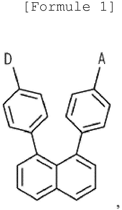
- an aspect of an embodiment of the invention provides a space-through charge transfer compound including a naphthalene core; an electron donor moiety selected from carbazole, phenylcarbazole and biphenylamine; and an electron acceptor moiety selected from pyridine, diazine, pyrrole, diazole, triazole and phenyl benzodiazole, wherein the electron donor moiety and the electron acceptor moiety are combined to first and eighth positions of the naphthalene core with a benzene linker, respectively.
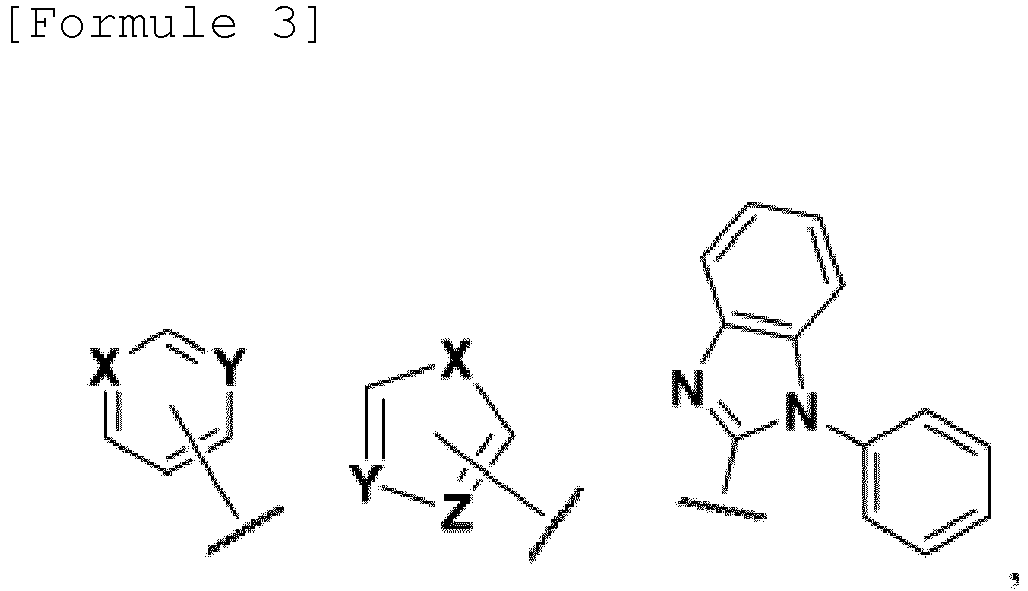
- a space-through charge transfer compound of Formula 1 wherein D is selected from and A is selected from wherein R is selected from hydrogen, C1 ⁇ C8 alkyl and C6 ⁇ C20 aryl, and wherein X, Y, Z are independently selected from carbon and nitrogen, and at least one selected from X and Y is nitrogen.
- an organic light emitting diode including a first electrode; a second electrode facing the first electrode; and an organic emitting layer between the first and second electrodes and including a space-through charge transfer compound, wherein the space-through charge transfer compound includes a naphthalene core, an electron donor moiety selected from carbazole and phenylcarbazole, and an electron acceptor moiety selected from pyridine, diazine, triazole and phenyl benzodiazole, and wherein the electron donor moiety and the electron acceptor moiety are combined to first and eighth positions of the naphthalene core with a benzene linker, respectively.
- the space-through charge transfer compound includes a naphthalene core, an electron donor moiety selected from carbazole and phenylcarbazole, and an electron acceptor moiety selected from pyridine, diazine, triazole and phenyl benzodiazole, and wherein the electron donor moiety and the electron acceptor moiety are combined to first and
- an organic light emitting diode including a first electrode; a second electrode facing the first electrode; and an organic emitting layer between the first and second electrodes and including a space-through charge transfer compound of wherein D is selected from and A is selected from wherein R is selected from hydrogen, C1 ⁇ C8 alkyl and C6 ⁇ C20 aryl, and wherein X, Y, Z are independently selected from carbon and nitrogen, and at least one selected from X and Y is nitrogen.
- a display device including a substrate; an organic light emitting diode on the substrate and including a first electrode, a second electrode facing the first electrode and an organic emitting layer between the first and second electrodes and including a space-through charge transfer compound; an encapsulation film on the organic light emitting diode; and a cover window on the encapsulation film, wherein the space-through charge transfer compound includes a naphthalene core, an electron donor moiety selected from carbazole and phenylcarbazole, and an electron acceptor moiety selected from pyridine, diazine, triazole and phenyl benzodiazole, and wherein the electron donor moiety and the electron acceptor moiety are combined to first and eighth positions of the naphthalene core with a benzene linker, respectively.
- the space-through charge transfer compound includes a naphthalene core, an electron donor moiety selected from carbazole and phenylcarbazole, and an electron acceptor moiety selected from pyr
- a display device including a substrate; an organic light emitting diode on the substrate and including a first electrode, a second electrode facing the first electrode and an organic emitting layer between the first and second electrodes and including a space-through charge transfer compound of Formula 1; an encapsulation film on the organic light emitting diode; and a cover window on the encapsulation film, wherein D is selected from and A is selected from wherein R is selected from hydrogen, C1 ⁇ C8 alkyl and C6 ⁇ C20 aryl, and wherein X, Y, Z are independently selected from carbon and nitrogen, and at least one selected from X and Y is nitrogen.
- the meanings of "at least one selected from a first item, a second item, and a third item” includes not only each of the first item, the second item, and the third item, but also all combinations of these items that may be suggested from two or more ones of the first item, the second item, and the third item.
- any one element when any one element is referred to as being "on" another element, it can be directly on the upper surface of the other element or a third intervening element may also be present.
- a space-through charge transfer compound of the present invention has a structure in that an electron donor moiety and an electron acceptor moiety are combined to first and eighth positions of a naphthalene core with a benzene linker and has Formula 1 of following.
- the electron donor moiety "D" is selected from formula 2.
- R is hydrogen, C1 ⁇ C8 alkyl or C6 ⁇ C20 aryl.
- the electron donor moiety "D” may be selected from carbazole, phenylcarbazole and biphenylamine.
- the electron acceptor moiety "A” is selected from Formula 3.
- X, Y and Z are independently selected from carbon and nitrogen, and at least one selected from X and Y is nitrogen.
- X, Y and Z are same or different.
- the electron acceptor "A” may be selected from pyridine, diazine, triazole and phenyl benzodiazole.
- the electron donor moiety and the electron acceptor moiety are combined or linked in the molecule such that an overlap between highest occupied molecular orbital (HOMO) and lowest unoccupied molecular orbital (LUMO) is reduced.
- HOMO highest occupied molecular orbital
- LUMO lowest unoccupied molecular orbital
- the triplet exciton is used to the emission such that the emitting efficiency is improved.
- the space-through charge transfer compound of the present invention includes both of the electron donor moiety and the electron acceptor moiety, the charge is easily transferred in the molecule, and the emission efficiency is improved.
- the space-through charge transfer compound of the present invention since the electron donor moiety and the electron acceptor moiety are combined or linked to the first and eighth positions of the naphthalene core, a gap or a distance between the electron donor moiety and the electron acceptor moiety is decreased or minimized. Accordingly, the charge transfer is directly generated through a space between the electron donor moiety and the electron acceptor moiety such that the conjugation length in the space-through charge transfer compound becomes shorter than other compound where the charge transfer is generated through a bonding orbital. As a result, a red shift problem in the emitted light can be prevented, and the space-through charge transfer compound of the present invention can provide the deep blue emission.
- the space-through charge transfer compound of the present invention includes the benzene linker being capable of minimizing the steric hinderance between the electron donor acceptor moiety and the electron acceptor moiety such that the stability of the compound is increased.
- FIG. 1 is a view illustrating an emission mechanism of a space-through charge transfer compound according to the present invention
- the triplet excitons as well as the singlet excitons are engaged in the emission such that the emitting efficiency is improved.
- the triplet exciton is activated by a field, and the triplet exciton and the singlet exciton are transferred into an intermediated state "I 1 " and transited into a ground state “So” to emit the light.
- the singlet state "S 1 " and the triplet state “T 1 " are transited into the intermediated state "I 1 " (S 1 -> I 1 ⁇ -T 1 ), and the singlet exciton and the triplet exciton in the intermediated state "I 1 " are engaged in the emission such that the emitting efficiency is improved.
- the compound having the above emission mechanism may be referred to as a field activated delayed fluorescence (FADF) compound.
- FADF field activated delayed fluorescence
- the dipole moment is generated in a polarized state.
- the interaction between the HOMO and the LUMO is further reduced such that the emission mechanism does not comply the Selection Rule. Accordingly, in the FADF compound, the transition from the triplet state "T 1 " and the singlet state "S 1 " into the intermediated state "I 1 " can be generated such that the triplet exciton can be engaged in the emission.
- the intersystem transition (intersystem crossing) from 25% singlet state “S 1 " excitons and 75% triplet state “T 1 " excitons to the intermediated state "I 1 " is generated, and the singlet and triplet excitons in the intermediated state "I 1 " are transited into the ground state to emit the light.
- the FADF compound has the theoretic quantum efficiency of 100%.
- the space-through charge transfer compound in the Formula 1 may be one of compounds in Formula 4. (Compounds 1 to 17 in an order)
- the space-through charge transfer compound of the present invention has a wide energy band gap such that the emission efficiency of the OLED using the compound is improved.
- HOMO HOMO
- LUMO eV
- Band gap compound 1 -5.53 -1.57 3.96 compound 2 -5.54 -1.64 3.90 compound 3 -5.57 -1.72 3.85 compound 4 -5.55 -1.69 3.86 compound 5 -5.54 -1.77 3.77 compound 6 -5.89 -1.55 4.34 compound 7 -5.86 -1.62 4.24 compound 8 -5.87 -1.70 4.17 compound 9 -5.86 -1.65 4.21 compound 10 -5.86 -1.81 4.05 compound 11 -5.17 -1.70 3.47 compound 12 -5.18 -1.59 3.59
- compound A compound B of 0.9 equivalent, Pd(0) of 0.05 equivalent and potassium carbonate of 4.0 equivalent were put into toluene, and the mixture was stirred in an oil bath under a temperature of 80 °C. 16 hours after, water was added into the mixture to be extracted, and the resultant was columned using the developing solvent of hexane and methyl chloride (2:1) such that compound C of white solid was obtained.
- compound E compound E, compound F of 0.9 equivalent, Pd(0) of 0.05 equivalent and potassium carbonate of 4.0 equivalent were put into toluene, and the mixture was stirred in an oil bath under a temperature of 80 °C. 16 hours after, water was added into the mixture to be extracted, and the resultant was columned using the developing solvent of hexane such that compound G of white solid was obtained.
- compound G compound G, compound D of 1.2 equivalent, Pd(0) of 0.05 equivalent and potassium carbonate of 4.0 equivalent were put into toluene, and the mixture was stirred in an oil bath under a temperature of 80 °C. 16 hours after, water was added into the mixture to be extracted, and the resultant was columned using the developing solvent of hexane and ethylene acetate (8:2) such that the compound 1 of white solid was obtained.
- compound A compound B of 0.9 equivalent, Pd(0) of 0.05 equivalent and potassium carbonate of 4.0 equivalent were put into toluene, and the mixture was stirred in an oil bath under a temperature of 80 °C. 16 hours after, water was added into the mixture to be extracted, and the resultant was columned using the developing solvent of hexane and methyl chloride (2:1) such that compound C of white solid was obtained.
- compound E compound E, compound F of 0.9 equivalent, Pd(0) of 0.05 equivalent and potassium carbonate of 4.0 equivalent were put into toluene, and the mixture was stirred in an oil bath under a temperature of 80 °C. 16 hours after, water was added into the mixture to be extracted, and the resultant was columned using the developing solvent of hexane such that compound G of white solid was obtained.
- compound G compound G, compound D of 1.2 equivalent, Pd(0) of 0.05 equivalent and potassium carbonate of 4.0 equivalent were put into toluene, and the mixture was stirred in an oil bath under a temperature of 80 °C. 16 hours after, water was added into the mixture to be extracted, and the resultant was columned using the developing solvent of hexane and ethylene acetate (8:2) such that the compound 2 of white solid was obtained.
- compound A compound B of 0.9 equivalent, Pd(0) of 0.05 equivalent and potassium carbonate of 4.0 equivalent were put into toluene, and the mixture was stirred in an oil bath under a temperature of 80 °C. 16 hours after, water was added into the mixture to be extracted, and the resultant was columned using the developing solvent of hexane and methyl chloride (2:1) such that compound C of white solid was obtained.
- compound E compound E, compound F of 0.9 equivalent, Pd(0) of 0.05 equivalent and potassium carbonate of 4.0 equivalent were put into toluene, and the mixture was stirred in an oil bath under a temperature of 80 °C. 16 hours after, water was added into the mixture to be extracted, and the resultant was columned using the developing solvent of hexane such that compound G of white solid was obtained.
- compound G compound G, compound D of 1.2 equivalent, Pd(0) of 0.05 equivalent and potassium carbonate of 4.0 equivalent were put into toluene, and the mixture was stirred in an oil bath under a temperature of 80 °C. 16 hours after, water was added into the mixture to be extracted, and the resultant was columned using the developing solvent of hexane and ethylene acetate (9:1) such that the compound 3 of white solid was obtained.
- compound D compound D, compound E of 0.9 equivalent, Pd(0) of 0.05 equivalent and potassium carbonate of 4.0 equivalent were put into toluene, and the mixture was stirred in an oil bath under a temperature of 80 °C. 16 hours after, water was added into the mixture to be extracted, and the resultant was columned using the developing solvent of hexane such that compound F of white solid was obtained.
- compound F compound F, compound C of 1.2 equivalent, Pd(0) of 0.05 equivalent and potassium carbonate of 4.0 equivalent were put into toluene, and the mixture was stirred in an oil bath under a temperature of 80 °C. 16 hours after, water was added into the mixture to be extracted, and the resultant was columned using the developing solvent of hexane and ethylene acetate (6:4) such that the compound 4 of white solid was obtained.
- compound A compound A, compound B of 0.9 equivalent, Pd(0) of 0.05 equivalent and potassium carbonate of 4.0 equivalent were put into toluene, and the mixture was stirred in an oil bath under a temperature of 80 °C. 16 hours after, water was added into the mixture to be extracted, and the resultant was columned using the developing solvent of hexane such that compound C of white solid was obtained.
- compound E compound E, compound F of 0.9 equivalent, Pd(0) of 0.05 equivalent and potassium carbonate of 4.0 equivalent were put into toluene, and the mixture was stirred in an oil bath under a temperature of 80 °C. 16 hours after, water was added into the mixture to be extracted, and the resultant was columned using the developing solvent of hexane such that compound G of white solid was obtained.
- compound G compound G, compound D of 1.2 equivalent, Pd(0) of 0.05 equivalent and potassium carbonate of 4.0 equivalent were put into toluene, and the mixture was stirred in an oil bath under a temperature of 80 °C. 16 hours after, water was added into the mixture to be extracted, and the resultant was columned using the developing solvent of hexane and methylene chloride (7:3) such that the compound 5 of white solid was obtained.
- compound A compound B of 0.9 equivalent, Pd(0) of 0.05 equivalent and potassium carbonate of 4.0 equivalent were put into toluene, and the mixture was stirred in an oil bath under a temperature of 80 °C. 16 hours after, water was added into the mixture to be extracted, and the resultant was columned using the developing solvent of hexane and methyl chloride (2:1) such that compound C of white solid was obtained.
- compound E compound E, compound F of 0.9 equivalent, Pd(0) of 0.05 equivalent and potassium carbonate of 4.0 equivalent were put into toluene, and the mixture was stirred in an oil bath under a temperature of 80 °C. 12 hours after, water was added into the mixture to be extracted, and the resultant was columned using the developing solvent of hexane such that compound G of white solid was obtained.
- compound I compound I, compound H of 0.9 equivalent, Pd(0) of 0.05 equivalent and potassium carbonate of 4.0 equivalent were put into toluene, and the mixture was stirred in an oil bath under a temperature of 80 °C. 8 hours after, water was added into the mixture to be extracted, and the resultant was columned using the developing solvent of hexane such that compound J of white solid was obtained.
- compound J compound J, compound D of 1.2 equivalent, Pd(0) of 0.05 equivalent and potassium carbonate of 4.0 equivalent were put into toluene, and the mixture was stirred in an oil bath under a temperature of 80 °C. 16 hours after, water was added into the mixture to be extracted, and the resultant was columned using the developing solvent of hexane and ethylene acetate (8:2) such that the compound 6 of white solid was obtained.
- compound A compound B of 0.9 equivalent, Pd(0) of 0.05 equivalent and potassium carbonate of 4.0 equivalent were put into toluene, and the mixture was stirred in an oil bath under a temperature of 80 °C. 16 hours after, water was added into the mixture to be extracted, and the resultant was columned using the developing solvent of hexane and methyl chloride (2:1) such that compound C of white solid was obtained.
- compound E compound E, compound F of 0.9 equivalent, Pd(0) of 0.05 equivalent and potassium carbonate of 4.0 equivalent were put into toluene, and the mixture was stirred in an oil bath under a temperature of 80 °C. 12 hours after, water was added into the mixture to be extracted, and the resultant was columned using the developing solvent of hexane such that compound G of white solid was obtained.
- compound I compound I, compound H of 0.9 equivalent, Pd(0) of 0.05 equivalent and potassium carbonate of 4.0 equivalent were put into toluene, and the mixture was stirred in an oil bath under a temperature of 80 °C. 8 hours after, water was added into the mixture to be extracted, and the resultant was columned using the developing solvent of hexane such that compound J of white solid was obtained.
- compound J compound J, compound D of 1.2 equivalent, Pd(0) of 0.05 equivalent and potassium carbonate of 4.0 equivalent were put into toluene, and the mixture was stirred in an oil bath under a temperature of 80 °C. 16 hours after, water was added into the mixture to be extracted, and the resultant was columned using the developing solvent of hexane and ethylene acetate (8:2) such that the compound 7 of white solid was obtained.
- compound A compound B of 0.9 equivalent, Pd(0) of 0.05 equivalent and potassium carbonate of 4.0 equivalent were put into toluene, and the mixture was stirred in an oil bath under a temperature of 80 °C. 16 hours after, water was added into the mixture to be extracted, and the resultant was columned using the developing solvent of hexane and methyl chloride (2:1) such that compound C of white solid was obtained.
- compound E compound E, compound F of 0.9 equivalent, Pd(0) of 0.05 equivalent and potassium carbonate of 4.0 equivalent were put into toluene, and the mixture was stirred in an oil bath under a temperature of 80 °C. 12 hours after, water was added into the mixture to be extracted, and the resultant was columned using the developing solvent of hexane such that compound G of white solid was obtained.
- compound I compound I, compound H of 0.9 equivalent, Pd(0) of 0.05 equivalent and potassium carbonate of 4.0 equivalent were put into toluene, and the mixture was stirred in an oil bath under a temperature of 80 °C. 8 hours after, water was added into the mixture to be extracted, and the resultant was columned using the developing solvent of hexane such that compound J of white solid was obtained.
- compound J compound J, compound D of 1.2 equivalent, Pd(0) of 0.05 equivalent and potassium carbonate of 4.0 equivalent were put into toluene, and the mixture was stirred in an oil bath under a temperature of 80 °C. 16 hours after, water was added into the mixture to be extracted, and the resultant was columned using the developing solvent of hexane and ethylene acetate (9:1) such that the compound 8 of white solid was obtained.
- compound D compound D, compound E of 0.9 equivalent, Pd(0) of 0.05 equivalent and potassium carbonate of 4.0 equivalent were put into toluene, and the mixture was stirred in an oil bath under a temperature of 80 °C. 12 hours after, water was added into the mixture to be extracted, and the resultant was columned using the developing solvent of hexane such that compound F of white solid was obtained.
- compound H compound H, compound G of 0.9 equivalent, Pd(0) of 0.05 equivalent and potassium carbonate of 4.0 equivalent were put into toluene, and the mixture was stirred in an oil bath under a temperature of 80 °C. 8 hours after, water was added into the mixture to be extracted, and the resultant was columned using the developing solvent of hexane such that compound I of white solid was obtained.
- compound I compound I, compound C of 1.2 equivalent, Pd(0) of 0.05 equivalent and potassium carbonate of 4.0 equivalent were put into toluene, and the mixture was stirred in an oil bath under a temperature of 80 °C. 16 hours after, water was added into the mixture to be extracted, and the resultant was columned using the developing solvent of hexane and ethylene acetate (9:1) such that the compound 9 of white solid was obtained.
- compound A compound A, compound B of 0.9 equivalent, Pd(0) of 0.05 equivalent and potassium carbonate of 4.0 equivalent were put into toluene, and the mixture was stirred in an oil bath under a temperature of 80 °C. 16 hours after, water was added into the mixture to be extracted, and the resultant was columned using the developing solvent of hexane such that compound C of white solid was obtained.
- compound E compound E, compound F of 0.9 equivalent, Pd(0) of 0.05 equivalent and potassium carbonate of 4.0 equivalent were put into toluene, and the mixture was stirred in an oil bath under a temperature of 80 °C. 12 hours after, water was added into the mixture to be extracted, and the resultant was columned using the developing solvent of hexane such that compound G of white solid was obtained.
- compound I compound I, compound H of 0.9 equivalent, Pd(0) of 0.05 equivalent and potassium carbonate of 4.0 equivalent were put into toluene, and the mixture was stirred in an oil bath under a temperature of 80 °C. 8 hours after, water was added into the mixture to be extracted, and the resultant was columned using the developing solvent of hexane such that compound J of white solid was obtained.
- compound J compound J, compound D of 1.2 equivalent, Pd(0) of 0.05 equivalent and potassium carbonate of 4.0 equivalent were put into toluene, and the mixture was stirred in an oil bath under a temperature of 80 °C. 16 hours after, water was added into the mixture to be extracted, and the resultant was columned using the developing solvent of hexane and methylene chloride (7:3) such that the compound 10 of white solid was obtained.
- compound F compound F, compound E of 0.9 equivalent, Pd(0) of 0.05 equivalent and potassium carbonate of 4.0 equivalent were put into toluene, and the mixture was stirred in an oil bath under a temperature of 80 °C. 12 hours after, water was added into the mixture to be extracted, and the resultant was columned using the developing solvent of hexane such that compound G of white solid was obtained.
- compound G compound G, compound C of 1.2 equivalent, Pd(0) of 0.05 equivalent and potassium carbonate of 4.0 equivalent were put into toluene, and the mixture was stirred in an oil bath under a temperature of 80 °C. 18 hours after, water was added into the mixture to be extracted, and the resultant was columned using the developing solvent of hexane and methylene chloride (6:4) such that the compound 11 of white solid was obtained.
- compound A compound B of 0.9 equivalent, Pd(0) of 0.05 equivalent and potassium carbonate of 4.0 equivalent were put into toluene, and the mixture was stirred in an oil bath under a temperature of 80 °C. 16 hours after, water was added into the mixture to be extracted, and the resultant was columned using the developing solvent of hexane and methyl chloride (2:1) such that compound C of white solid was obtained.
- compound F compound F, compound E of 0.9 equivalent, Pd(0) of 0.05 equivalent and potassium carbonate of 4.0 equivalent were put into toluene, and the mixture was stirred in an oil bath under a temperature of 80 °C. 12 hours after, water was added into the mixture to be extracted, and the resultant was columned using the developing solvent of hexane such that compound G of white solid was obtained.
- compound G compound G, compound D of 1.2 equivalent, Pd(0) of 0.05 equivalent and potassium carbonate of 4.0 equivalent were put into toluene, and the mixture was stirred in an oil bath under a temperature of 80 °C. 18 hours after, water was added into the mixture to be extracted, and the resultant was columned using the developing solvent of hexane and methylene chloride (8:2) such that the compound 12 of white solid was obtained.
- compound A compound B of 0.9 equivalent, Pd(0) of 0.05 equivalent and potassium carbonate of 4.0 equivalent were put into toluene, and the mixture was stirred in an oil bath under a temperature of 80 °C. 16 hours after, water was added into the mixture to be extracted, and the resultant was columned using the developing solvent of hexane and methyl chloride (2:1) such that compound C of white solid was obtained.
- compound E compound E, compound F of 0.9 equivalent, Pd(0) of 0.05 equivalent and potassium carbonate of 4.0 equivalent were put into toluene, and the mixture was stirred in an oil bath under a temperature of 80 °C. 12 hours after, water was added into the mixture to be extracted, and the resultant was columned using the developing solvent of hexane such that compound G of white solid was obtained.
- compound I compound I, compound H of 0.9 equivalent, Pd(0) of 0.05 equivalent and potassium carbonate of 4.0 equivalent were put into toluene, and the mixture was stirred in an oil bath under a temperature of 80 °C. 8 hours after, water was added into the mixture to be extracted, and the resultant was columned using the developing solvent of hexane such that compound J of white solid was obtained.
- compound J compound J, compound D of 1.2 equivalent, Pd(0) of 0.05 equivalent and potassium carbonate of 4.0 equivalent were put into toluene, and the mixture was stirred in an oil bath under a temperature of 80 °C. 16 hours after, water was added into the mixture to be extracted, and the resultant was columned using the developing solvent of hexane and ethylene acetate (8:2) such that the compound 13 of white solid was obtained.
- compound A compound B of 0.9 equivalent, Pd(0) of 0.05 equivalent and potassium carbonate of 4.0 equivalent were put into toluene, and the mixture was stirred in an oil bath under a temperature of 80 °C. 16 hours after, water was added into the mixture to be extracted, and the resultant was columned using the developing solvent of hexane and methyl chloride (2:1) such that compound C of white solid was obtained.
- compound E compound E, compound F of 0.9 equivalent, Pd(0) of 0.05 equivalent and potassium carbonate of 4.0 equivalent were put into toluene, and the mixture was stirred in an oil bath under a temperature of 80 °C. 12 hours after, water was added into the mixture to be extracted, and the resultant was columned using the developing solvent of hexane such that compound G of white solid was obtained.
- compound I compound I, compound H of 0.9 equivalent, Pd(0) of 0.05 equivalent and potassium carbonate of 4.0 equivalent were put into toluene, and the mixture was stirred in an oil bath under a temperature of 80 °C. 8 hours after, water was added into the mixture to be extracted, and the resultant was columned using the developing solvent of hexane such that compound J of white solid was obtained.
- compound J compound J, compound D of 1.2 equivalent, Pd(0) of 0.05 equivalent and potassium carbonate of 4.0 equivalent were put into toluene, and the mixture was stirred in an oil bath under a temperature of 80 °C. 16 hours after, water was added into the mixture to be extracted, and the resultant was columned using the developing solvent of hexane and ethylene acetate (8:2) such that the compound 14 of white solid was obtained.
- compound A compound B of 0.9 equivalent, Pd(0) of 0.05 equivalent and potassium carbonate of 4.0 equivalent were put into toluene, and the mixture was stirred in an oil bath under a temperature of 80 °C. 16 hours after, water was added into the mixture to be extracted, and the resultant was columned using the developing solvent of hexane and methyl chloride (2:1) such that compound C of white solid was obtained.
- compound E compound E, compound F of 0.9 equivalent, Pd(0) of 0.05 equivalent and potassium carbonate of 4.0 equivalent were put into toluene, and the mixture was stirred in an oil bath under a temperature of 80 °C. 12 hours after, water was added into the mixture to be extracted, and the resultant was columned using the developing solvent of hexane such that compound G of white solid was obtained.
- compound I compound I, compound H of 0.9 equivalent, Pd(0) of 0.05 equivalent and potassium carbonate of 4.0 equivalent were put into toluene, and the mixture was stirred in an oil bath under a temperature of 80 °C. 8 hours after, water was added into the mixture to be extracted, and the resultant was columned using the developing solvent of hexane such that compound J of white solid was obtained.
- compound J compound J, compound D of 1.2 equivalent, Pd(0) of 0.05 equivalent and potassium carbonate of 4.0 equivalent were put into toluene, and the mixture was stirred in an oil bath under a temperature of 80 °C. 16 hours after, water was added into the mixture to be extracted, and the resultant was columned using the developing solvent of hexane and ethylene acetate (9:1) such that the compound 15 of white solid was obtained.
- compound D compound D, compound E of 0.9 equivalent, Pd(0) of 0.05 equivalent and potassium carbonate of 4.0 equivalent were put into toluene, and the mixture was stirred in an oil bath under a temperature of 80 °C. 12 hours after, water was added into the mixture to be extracted, and the resultant was columned using the developing solvent of hexane such that compound F of white solid was obtained.
- compound H compound H, compound G of 0.9 equivalent, Pd(0) of 0.05 equivalent and potassium carbonate of 4.0 equivalent were put into toluene, and the mixture was stirred in an oil bath under a temperature of 80 °C. 8 hours after, water was added into the mixture to be extracted, and the resultant was columned using the developing solvent of hexane such that compound I of white solid was obtained.
- compound I compound I, compound C of 1.2 equivalent, Pd(0) of 0.05 equivalent and potassium carbonate of 4.0 equivalent were put into toluene, and the mixture was stirred in an oil bath under a temperature of 80 °C. 16 hours after, water was added into the mixture to be extracted, and the resultant was columned using the developing solvent of hexane and ethylene acetate (9:1) such that the compound 16 of white solid was obtained.
- compound A compound A, compound B of 0.9 equivalent, Pd(0) of 0.05 equivalent and potassium carbonate of 4.0 equivalent were put into toluene, and the mixture was stirred in an oil bath under a temperature of 80 °C. 16 hours after, water was added into the mixture to be extracted, and the resultant was columned using the developing solvent of hexane such that compound C of white solid was obtained.
- compound E compound E, compound F of 0.9 equivalent, Pd(0) of 0.05 equivalent and potassium carbonate of 4.0 equivalent were put into toluene, and the mixture was stirred in an oil bath under a temperature of 80 °C. 12 hours after, water was added into the mixture to be extracted, and the resultant was columned using the developing solvent of hexane such that compound G of white solid was obtained.
- compound I compound I, compound H of 0.9 equivalent, Pd(0) of 0.05 equivalent and potassium carbonate of 4.0 equivalent were put into toluene, and the mixture was stirred in an oil bath under a temperature of 80 °C. 8 hours after, water was added into the mixture to be extracted, and the resultant was columned using the developing solvent of hexane such that compound J of white solid was obtained.
- compound J compound J, compound D of 1.2 equivalent, Pd(0) of 0.05 equivalent and potassium carbonate of 4.0 equivalent were put into toluene, and the mixture was stirred in an oil bath under a temperature of 80 °C. 16 hours after, water was added into the mixture to be extracted, and the resultant was columned using the developing solvent of hexane and methylene chloride (7:3) such that the compound 17 of white solid was obtained.
- MAP maximum absorption peak
- MEP maximum emission peak
- Stocks-shift value of the above compounds 1 and 2 and reference compounds in Formulas 5 and 6 are listed in Tables 2 to 5, respectively.
- the space-through charge transfer compounds of the present invention has the maximum absorption peak of 338nm regardless the kinds of the solvents, while the emission spectrums are various according to the kinds of the solvents. Namely, the space-through charge transfer compound of the present invention has a relatively low maximum emission peak in the solvent of toluene having a relatively low polarity and a relatively high maximum emission peak in the solvent of CHCl 3 and THF having a relatively low polarity. As a result, as the polarity of the solvent is increased, the maximum emission peak of the space-through charge transfer compound is red-shifted.
- the reference compounds (Ref1 and Ref2) only show the fluorescent emission (Prompt).
- the space-through charge transfer compounds (Com1 and Com2) of the present invention show the delayed fluorescent emission (Delayed) of hundreds of thousands nano-seconds (ns) with the fluorescent emission (Prompt).
- the space-through charge transfer compound of the present invention is activated by the field such that the excitons in the singlet state “S 1 " and the triplet state “T 1 " are transited into the intermediated state "I 1 ".
- both the exciton in the singlet state "S 1 " and the exciton in the triplet state “T 1 " are engaged in the emission.
- the FADF compound is a single molecule compound having the electron donor moiety and the electron acceptor moiety in the single molecule such that the charge transfer is easily generated through a space in the molecule.
- the charge can be separated from the electron donor moiety to the electron acceptor moiety through the space between the electron donor moiety to the electron acceptor moiety.
- the FADF compound is activated by outer factors. It can be verified by comparing the absorption peak and the emission peak of the solution of the compounds.
- ⁇ ⁇ " is the Stock-shift value
- ⁇ abs and ⁇ fl are the wave-number of the maximum absorption peak and the maximum emission peak, respectively.
- h is Planck's constant
- c is the velocity of light
- a is the onsager cavity radius
- ⁇ is a difference between the dipole moment of the excited state and the dipole moment of the ground state.
- ⁇ f is a value indicating the orientational polarizability of the solvent and may be a function of the dielectric constant of the solvent ( ⁇ ) and the refractive index of the solvent (n).
- ⁇ f ⁇ ⁇ 1 2 ⁇ + 1 ⁇ n 2 ⁇ 1 2 n 2 + 1
- the FADF can be verified by comparing the absorption peak and the emission peak of the solution of the compounds.
- the orientational polarizability ( ⁇ f) of the mixed solvent can be calculated by using the orientational polarizability of each pure solvent and their mole fraction.
- ⁇ f and ⁇ ⁇ are linearly plotted by using above “Lippert-Mataga equation”
- the compound may provide the FADF emission.
- the compounds 1 and 2 provides the linear relation (R 2 >0.90). Namely, the compounds 1 and 2 provide the FADF emission where both the singlet exciton and the triplet exciton are engaged in the emission.
- FIG. 4C which is "Lippert-Mataga plot" graphs of the reference compound 1 (Ref1) in the Formula 5, the reference compound 1 also provides the linear relation.
- the reference compound 1 (Ref1) since the charge is transferred through the bonding orbital of the molecule, the conjugation length is increased such that the red-shift problem is generated.
- the 25% excitons in the singlet state and the 75% excitons in the triplet state are transited into the intermediate state by an outer force, i.e., a field generated when the OLED is driven.
- the excitons in the intermediate state are transited into the ground state such that the emitting efficiency is improved. Namely, in the fluorescent compound, since the singlet exciton and the triplet exciton are engaged in the emission, the emitting efficiency is improved.
- An ITO layer is deposited on a substrate and washed to form an anode (3mm*3mm).
- the substrate is loaded in a vacuum chamber, and a hole injecting layer (40 ⁇ , NPB(N,N'-di(naphthalen-1-yl)-N,N'-diphenyl-benzidine)), a hole transporting layer (10 ⁇ , mCP(N,N'-Dicarbazolyl-3,5-benzene)), an emitting material layer (200 ⁇ , host (bis ⁇ 2-[di(phenyl)phosphino]phenyl ⁇ ether oxide) and dopant (12%)), an electron transporting layer (300 ⁇ , 1,3,5-tri(phenyl-2-benzimidazole)-benzene), an electron injecting layer (10 ⁇ , LiF), and a cathode (Al) are sequentially formed on the anode under a base pressure of about 10 -6 to 10 -7 Torr.
- a hole injecting layer 40 ⁇ , NPB(N,
- the compound 1 is used as the dopant to form the OLED.
- the compound 2 is used as the dopant to form the OLED.
- the compound 11 is used as the dopant to form the OLED.
- the compound 12 is used as the dopant to form the OLED.
- the compound 13 is used as the dopant to form the OLED.
- the compound 14 is used as the dopant to form the OLED.
- the reference compound 1 in the Formula 5 is used as the dopant to form the OLED.
- the reference compound 2 in the Formula 6 is used as the dopant to form the OLED.
- Table 7 Voltage (V) Efficiency EQE (%) CIE(X) CIE(Y) Cd/A Lm/W Ex1 4.3 6.1 4.4 6.8 0.142 0.092 Ex2 4.5 6.4 4.5 6.9 0.143 0.089 Ex3 4.2 9.2 6.9 9.7 0.157 0.136 Ex4 4.4 8.8 6.3 9.2 0.149 0.127 Ex5 4.3 6.7 4.9 7.0 0.148 0.097 Ex6 4.4 7.3 5.2 8.1 0.151 0.103 Ref1 4.7 5.9 3.9 6.3 0.142 0.203 Ref2 4.6 4.2 4.2 4.7 0.144 0.091
- the OLEDs using the compounds of the present invention (Ex1 to Ex6) and the OLED using the reference compound 1 (Ref1) have the improved efficiency. However, there is difference in the color purity. Namely, in comparison to the OLED using the reference compound 1 (Ref1), the OLEDs using the compounds of the present invention (Ex1 to Ex6) provide the deep blue image.
- the OLEDs using the compounds of the present invention (Ex1 to Ex6) and the OLED using the reference compound 2 (Ref2) have similar color purity. However, there is difference in the emitting efficiency. Namely, in comparison to the OLED using the reference compound 2 (Ref2), the OLEDs using the compounds of the present invention (Ex1 to Ex6), which is the charge transfer complex, have excellent emitting efficiency.
- the OLED using the space-through charge transfer compound of the present invention has advantages in both the emitting efficiency and the color purity.
- FIG. 5 is a schematic cross-sectional view of an OLED according to the invention.
- the OLED “E” is formed on a substrate (not shown).
- the OLED “E” includes a first electrode 110 as an anode, a second electrode 130 as a cathode and an organic emitting layer 120 therebetween.
- an encapsulation film which includes at least one inorganic layer and at least one organic layer and covers the OLED "E", and a cover window on the encapsulation film may be further formed to form a display device including the OLED "E".
- the substrate, the encapsulation film and the cover window may have a flexible property such that a flexible display device may be provided.
- the first electrode 110 is formed of a material having a relatively high work function
- the second electrode 130 is formed of a material having a relatively low work function.
- the first electrode 110 may be formed of indium-tin-oxide (ITO)
- the second electrode 130 may be formed of aluminum (Al) or Al alloy (AlNd).
- the organic emitting layer 120 may include red, green and blue emitting patterns.
- the organic emitting layer 120 may have a single-layered structure.
- the organic emitting layer 120 includes a hole injection layer (HIL) 121, a hole transporting layer (HTL) 122, an emitting material layer (EML) 123, an electron transporting layer (ETL) 124 and an electron injection layer (EIL) 125 sequentially stacked on the first electrode 110.
- HIL hole injection layer
- HTL hole transporting layer
- EML electron transporting layer
- EIL electron injection layer
- At least one selected from the HIL 121, the HTL 122, the EML 123, the ETL 124 and the EIL 125 includes the space-through charge transfer compound in the Formula 1.
- the EML 123 may include the space-through charge transfer compound in the Formula 1.
- the space-through charge transfer compound acts as the dopant, and the EML 123 may further include a host to emit the blue light.
- the dopant has about 1 to 30 weight % with respect to the host.
- a difference between the HOMO of the host "HOMO Host” and the HOMO of the dopant "HOMO Dopant " or a difference between the LUMO of the host "LUMO Host " and the LUMO of the dopant "LUMO Dopant " is less than 0.5 eV. (
- the triplet energy of the dopant is smaller than the triplet energy of the host, and a difference between the singlet energy of the dopant and the triplet energy of the dopant is less than 0.3eV. ( ⁇ E ST ⁇ 0.3eV) As the difference " ⁇ E ST " is smaller, the emitting efficiency is higher. In the space-through charge transfer compound of the present invention, even if the difference " ⁇ E ST " between the singlet energy of the dopant and the triplet energy of the dopant is about 0.3eV, which is relatively large, the excitons in the singlet state "S 1 " and the excitons in the triplet state "T 1 " can be transited into the intermediate state "I 1 ".
- the host which meets the above condition, may be selected from materials in Formula 7.
- materials in Formula 7. Bis[2-(diphenylphosphino)phenyl]ether oxide (DPEPO), 2,8-bis(diphenylphosphoryl)dibenzothiophene (PPT), 2,8-di(9H-carbazol-9-yl)dibenzothiophene (DCzDBT), m-bis(carbazol-9-yl)biphenyl (m-CBP), Diphenyl-4-triphenylsilylphenyl-phosphine oxide (TPSO1), 9-(9-phenyl-9H-carbazol-6-yl)-9H-carbazole (CCP) in an order)
- DPEPO 2,8-bis(diphenylphosphoryl)dibenzothiophene
- DCzDBT 2,8-di(9H-carbazol-9-yl)dibenzothiophene
- m-CBP m-bis(
- the space-through charge transfer compound of the present invention may act as a host in the EML 123, and the EML 123 may further include a dopant to emit the blue light.
- the dopant has about 1 to 30 weight % with respect to the host. Since the development of the blue host having excellent properties is insufficient, the space-through charge transfer compound of the present invention may be used as the host to increase the degree of freedom for the host. In this instance, the triplet energy of the dopant may be smaller than the triplet energy of the host of the space-through charge transfer compound of the present invention.
- the EML 123 may include a first dopant of the space-through charge transfer compound of the present invention, a host and a second dopant.
- the weight % summation of the first and second dopants may be about 1 to 30 to emit the blue light. In this instance, the emitting efficiency and the color purity may be further improved.
- the triplet energy of the first dopant i.e., the space-through charge transfer compound of the present invention
- the triplet energy of the first dopant may be smaller than the triplet energy of the host and larger than the triplet energy of the second dopant.
- a difference between the singlet energy of the first dopant and the triplet energy of the first dopant is less than 0.3eV. ( ⁇ E ST ⁇ 0.3eV) As the difference " ⁇ E ST " is smaller, the emitting efficiency is higher.
- the space-through charge transfer compound of the present invention since the electron donor moiety and the electron acceptor moiety are combined or linked in one molecule and the overlap between the HOMO and the LUMO is decreased, the space-through charge transfer compound of the present invention acts as a charge transfer complex such that the emitting efficiency of the compound is improved. Namely, in the space-through charge transfer compound of the present invention, the excitons in the triplet state are engaged in the emission such that the emitting efficiency of the compound is improved.
- the electron donor moiety and the electron acceptor moiety are combined or linked to the first and eighth positions of the naphthalene core, a space between the electron donor moiety and the electron acceptor moiety is decreased or minimized. Accordingly, the charge transfer is directly generated through the space between the electron donor moiety and the electron acceptor moiety such that the conjugation length is decreased. As a result, the red shift problem in the emitted light is prevented. Namely, the OLED using the space-through charge transfer compound of the present invention can emit the deep blue light. Accordingly, the OLED using the space-through charge transfer compound of the present invention has advantages in the emitting efficiency and the image quality.
Landscapes
- Chemical & Material Sciences (AREA)
- Organic Chemistry (AREA)
- Engineering & Computer Science (AREA)
- Materials Engineering (AREA)
- Physics & Mathematics (AREA)
- Spectroscopy & Molecular Physics (AREA)
- Optics & Photonics (AREA)
- Microelectronics & Electronic Packaging (AREA)
- Electroluminescent Light Sources (AREA)
Claims (12)
- Composé de transfert de charge dans l'espace, comprenant :un noyau de naphtalène ;une fraction de donneur d'électron sélectionnée parmi le carbazole, phénylcarbazole et biphénylamine ; etune fraction d'accepteur d'électron sélectionnée parmi le pyridine, diazine, pyrrole, diazole, triazole et phényl benzodiazole,dans lequel la fraction de donneur d'électron et la fraction d'accepteur d'électron sont combinées à une première et huitième position du noyau de naphtalène avec un lieur benzène, respectivement.
- Composé de transfert de charge dans l'espace selon la revendication 1, qui est défini par la Formule 1 :


- Composé de transfert de charge dans l'espace selon la revendication 1 et/ou 2, dans lequel une différence entre l'énergie de singlet du composé de transfert de charge dans l'espace et une énergie de triplet du composé de transfert de charge dans l'espace est inférieure à 0,3eV.
- Diode électroluminescente organique, comprenant :une première électrode (110) ;une seconde électrode (130) faisant face à la première électrode ; etune couche organique émettrice (120) entre la première et la seconde électrode et incluant un composé de transfert de charge dans l'espace,dans lequel le composé de transfert de charge dans l'espace est défini comme dans la revendication 1.
- Diode électroluminescente organique selon la revendication 4, dans laquelle le composé de transfert de charge dans l'espace est défini par la Formule 1 :


- Diode électroluminescente organique selon la revendication 4 et/ou 5, dans laquelle la couche organique émettrice inclut une couche d'injection à trou (HIL)(121), une couche de transport à trou (HTL)(122), une couche de matériau émetteur (EML)(123), une couche de transport d'électron (ETL) (124) et une couche d'injection d'électron (EIL) (125), et
dans lequel au moins une sélectionnée parmi les HIL, HTL, EML, ETL et EIL inclut le composé de transfert de charge dans l'espace. - Diode électroluminescente organique selon une quelconque des revendications 4 à 6, dans laquelle une différence entre l'énergie de singlet du composé de transfert de charge dans l'espace et une énergie de triplet du composé de transfert de charge dans l'espace est inférieure à 0,3eV.
- Diode électroluminescente organique selon une quelconque des revendications 4 à 7, dans laquelle la couche organique émettrice inclut en outre un hôte et le composé de transfert de charge dans l'espace est utilisé comme un dopant.
- Diode électroluminescente organique selon la revendication 8, dans laquelle une différence entre un HOMO de l'hôte et un HOMO du dopant ou une différence entre le LUMO de l'hôte et le LUMO du dopant est inférieure à 0.5eV.
- Diode électroluminescente organique selon une quelconque des revendications 4 à 7, dans lequel la couche organique émettrice inclut en outre un dopant, et le composé de transfert de charge dans l'espace est utilisé comme un hôte.
- Diode électroluminescente organique selon une quelconque des revendications 4 à 7, dans laquelle la couche organique émettrice inclut en outre un hôte et un premier dopant, et le composé de transfert de charge dans l'espace est utilisé comme un second dopant, et
dans laquelle une énergie de triplet du second hôte est plus petite que l'énergie de triplet de l'hôte et plus grande que l'énergie de triplet du premier dopant. - Dispositif d'affichage, comprenant :un substrat ;une diode électroluminescente organique définie selon une quelconque des revendications 4 à 11 sur le substrat ;un film d'encapsulation sur la diode électroluminescente organique ; etune fenêtre de couverture sur le film d'encapsulation.
Applications Claiming Priority (2)
| Application Number | Priority Date | Filing Date | Title |
|---|---|---|---|
| KR20140140971 | 2014-10-17 | ||
| KR1020150129084A KR102440238B1 (ko) | 2014-10-17 | 2015-09-11 | 공간 전하 이동 화합물, 이를 포함하는 유기발광다이오드소자 및 표시장치 |
Publications (2)
| Publication Number | Publication Date |
|---|---|
| EP3010064A1 EP3010064A1 (fr) | 2016-04-20 |
| EP3010064B1 true EP3010064B1 (fr) | 2017-07-19 |
Family
ID=54291140
Family Applications (1)
| Application Number | Title | Priority Date | Filing Date |
|---|---|---|---|
| EP15188932.6A Active EP3010064B1 (fr) | 2014-10-17 | 2015-10-08 | Composé de transfert de charge dans l'espace et diode électroluminescente organique et dispositif d'affichage utilisant celui-ci |
Country Status (2)
| Country | Link |
|---|---|
| US (2) | US10141515B2 (fr) |
| EP (1) | EP3010064B1 (fr) |
Families Citing this family (6)
| Publication number | Priority date | Publication date | Assignee | Title |
|---|---|---|---|---|
| EP3010064B1 (fr) * | 2014-10-17 | 2017-07-19 | LG Display Co., Ltd. | Composé de transfert de charge dans l'espace et diode électroluminescente organique et dispositif d'affichage utilisant celui-ci |
| US10879471B2 (en) | 2017-05-10 | 2020-12-29 | Samsung Display Co., Ltd. | Organic electroluminescence device and amine compound for organic electroluminescence device |
| KR102516057B1 (ko) * | 2017-11-17 | 2023-03-31 | 삼성디스플레이 주식회사 | 유기 발광 소자 |
| CN108864068B (zh) * | 2018-07-27 | 2021-12-28 | 武汉天马微电子有限公司 | 一种化合物以及有机发光显示装置 |
| KR102784885B1 (ko) * | 2018-12-05 | 2025-03-20 | 엘지디스플레이 주식회사 | 유기 화합물, 이를 포함하는 유기발광다이오드 및 유기발광장치 |
| KR102773495B1 (ko) | 2020-02-10 | 2025-02-28 | 삼성디스플레이 주식회사 | 유기 발광 소자 |
Family Cites Families (7)
| Publication number | Priority date | Publication date | Assignee | Title |
|---|---|---|---|---|
| KR20070009306A (ko) * | 2005-07-15 | 2007-01-18 | 삼성에스디아이 주식회사 | 백색 유기 발광 소자의 제조 방법 |
| KR20100113204A (ko) * | 2009-04-13 | 2010-10-21 | 주식회사 엘지화학 | 새로운 유기 발광 소자 재료 및 이를 이용한 유기 발광 소자 |
| JP5783749B2 (ja) * | 2011-02-15 | 2015-09-24 | ケミプロ化成株式会社 | エキシマー特性を有する1,8−アリール置換ナフタレン誘導体及びこれを用いた有機el素子 |
| WO2013089424A1 (fr) * | 2011-12-12 | 2013-06-20 | 제일모직 주식회사 | Composé pour un dispositif opto-électrique organique, diode électroluminescente organique le comprenant et dispositif d'affichage comprenant la diode électroluminescente organique |
| KR101499356B1 (ko) * | 2013-06-28 | 2015-03-05 | 주식회사 엘지화학 | 헤테로환 화합물 및 이를 포함하는 유기 발광 소자 |
| KR101639867B1 (ko) * | 2013-07-08 | 2016-07-14 | 주식회사 엘지화학 | 헤테로환 화합물 및 이를 포함하는 유기 발광 소자 |
| EP3010064B1 (fr) * | 2014-10-17 | 2017-07-19 | LG Display Co., Ltd. | Composé de transfert de charge dans l'espace et diode électroluminescente organique et dispositif d'affichage utilisant celui-ci |
-
2015
- 2015-10-08 EP EP15188932.6A patent/EP3010064B1/fr active Active
- 2015-10-16 US US14/885,707 patent/US10141515B2/en active Active
-
2018
- 2018-10-11 US US16/158,087 patent/US10892419B2/en active Active
Non-Patent Citations (1)
| Title |
|---|
| None * |
Also Published As
| Publication number | Publication date |
|---|---|
| US10141515B2 (en) | 2018-11-27 |
| EP3010064A1 (fr) | 2016-04-20 |
| US10892419B2 (en) | 2021-01-12 |
| US20160111650A1 (en) | 2016-04-21 |
| US20190081244A1 (en) | 2019-03-14 |
Similar Documents
| Publication | Publication Date | Title |
|---|---|---|
| EP3009494B1 (fr) | Composé à fluorescence différée et diode électroluminescente organique et dispositif d'affichage utilisant celui-ci | |
| EP3029125B1 (fr) | Composé à fluorescence différée et diode électroluminescente organique et dispositif d'affichage utilisant celui-ci | |
| EP3020783B1 (fr) | Composé à fluorescence différée et diode électroluminescente organique et dispositif d'affichage utilisant celui-ci | |
| EP3389107B1 (fr) | Appareil électroluminescent el organique et instrument électronique | |
| EP3010052B1 (fr) | Composé à fluorescence différée et diode électroluminescente organique et dispositif d'affichage utilisant celui-ci | |
| EP2881446B1 (fr) | Composé organique et dispositif électroluminescent organique l'utilisant | |
| EP2665342B1 (fr) | Composition pour élément électroluminescent organique, élément électroluminesecent organique, dispositif d'affichage et dispositif d'éclairage | |
| KR101597855B1 (ko) | 유기 발광 소자 및 이에 사용하기 위한 재료 | |
| KR101583097B1 (ko) | 유기 el 소자 및 유기 el 재료 함유 용액 | |
| US9153790B2 (en) | Organic electroluminescent device | |
| EP2085371B1 (fr) | Composé de fluoranthène, dispositif électroluminescent organique utilisant le composé de fluoranthène et solution contenant un matériau électroluminescent organique | |
| EP2434559B1 (fr) | Élément électroluminescent organique | |
| US9812661B2 (en) | Organic electroluminescent device | |
| EP3010064B1 (fr) | Composé de transfert de charge dans l'espace et diode électroluminescente organique et dispositif d'affichage utilisant celui-ci | |
| US20060222886A1 (en) | Arylpyrene compounds | |
| US7794855B2 (en) | Compound and organic light-emitting element | |
| EP2434558A1 (fr) | Élément électroluminescent organique | |
| CN105601613B (zh) | 空间电荷转移化合物和使用该化合物的有机发光二极管和显示装置 | |
| CN116761868A (zh) | 有机电致发光元件、有机电致发光显示装置和电子设备 | |
| EP3029753B1 (fr) | Composé de transfert de charge dans l'espace et diode électroluminescente organique et dispositif d'affichage utilisant celui-ci | |
| US20100156285A1 (en) | Trinaphthyl monoamine or derivative thereof, organic electroluminescent device using the same, and organic electroluminescent material-containing solution | |
| KR100881573B1 (ko) | 유기 전계발광 소자 | |
| KR102954603B1 (ko) | 유기 전계발광 재료 및 유기 전계발광 디바이스 |
Legal Events
| Date | Code | Title | Description |
|---|---|---|---|
| PUAI | Public reference made under article 153(3) epc to a published international application that has entered the european phase |
Free format text: ORIGINAL CODE: 0009012 |
|
| 17P | Request for examination filed |
Effective date: 20151008 |
|
| AK | Designated contracting states |
Kind code of ref document: A1 Designated state(s): AL AT BE BG CH CY CZ DE DK EE ES FI FR GB GR HR HU IE IS IT LI LT LU LV MC MK MT NL NO PL PT RO RS SE SI SK SM TR |
|
| AX | Request for extension of the european patent |
Extension state: BA ME |
|
| RBV | Designated contracting states (corrected) |
Designated state(s): AL AT BE BG CH CY CZ DE DK EE ES FI FR GB GR HR HU IE IS IT LI LT LU LV MC MK MT NL NO PL PT RO RS SE SI SK SM TR |
|
| GRAP | Despatch of communication of intention to grant a patent |
Free format text: ORIGINAL CODE: EPIDOSNIGR1 |
|
| INTG | Intention to grant announced |
Effective date: 20170202 |
|
| RAP1 | Party data changed (applicant data changed or rights of an application transferred) |
Owner name: LG DISPLAY CO., LTD. |
|
| GRAS | Grant fee paid |
Free format text: ORIGINAL CODE: EPIDOSNIGR3 |
|
| GRAA | (expected) grant |
Free format text: ORIGINAL CODE: 0009210 |
|
| AK | Designated contracting states |
Kind code of ref document: B1 Designated state(s): AL AT BE BG CH CY CZ DE DK EE ES FI FR GB GR HR HU IE IS IT LI LT LU LV MC MK MT NL NO PL PT RO RS SE SI SK SM TR |
|
| REG | Reference to a national code |
Ref country code: GB Ref legal event code: FG4D |
|
| REG | Reference to a national code |
Ref country code: CH Ref legal event code: EP |
|
| REG | Reference to a national code |
Ref country code: IE Ref legal event code: FG4D |
|
| REG | Reference to a national code |
Ref country code: AT Ref legal event code: REF Ref document number: 911158 Country of ref document: AT Kind code of ref document: T Effective date: 20170815 |
|
| REG | Reference to a national code |
Ref country code: DE Ref legal event code: R096 Ref document number: 602015003632 Country of ref document: DE |
|
| REG | Reference to a national code |
Ref country code: FR Ref legal event code: PLFP Year of fee payment: 3 |
|
| REG | Reference to a national code |
Ref country code: NL Ref legal event code: MP Effective date: 20170719 |
|
| REG | Reference to a national code |
Ref country code: LT Ref legal event code: MG4D |
|
| REG | Reference to a national code |
Ref country code: AT Ref legal event code: MK05 Ref document number: 911158 Country of ref document: AT Kind code of ref document: T Effective date: 20170719 |
|
| PG25 | Lapsed in a contracting state [announced via postgrant information from national office to epo] |
Ref country code: HR Free format text: LAPSE BECAUSE OF FAILURE TO SUBMIT A TRANSLATION OF THE DESCRIPTION OR TO PAY THE FEE WITHIN THE PRESCRIBED TIME-LIMIT Effective date: 20170719 Ref country code: NL Free format text: LAPSE BECAUSE OF FAILURE TO SUBMIT A TRANSLATION OF THE DESCRIPTION OR TO PAY THE FEE WITHIN THE PRESCRIBED TIME-LIMIT Effective date: 20170719 Ref country code: SE Free format text: LAPSE BECAUSE OF FAILURE TO SUBMIT A TRANSLATION OF THE DESCRIPTION OR TO PAY THE FEE WITHIN THE PRESCRIBED TIME-LIMIT Effective date: 20170719 Ref country code: AT Free format text: LAPSE BECAUSE OF FAILURE TO SUBMIT A TRANSLATION OF THE DESCRIPTION OR TO PAY THE FEE WITHIN THE PRESCRIBED TIME-LIMIT Effective date: 20170719 Ref country code: FI Free format text: LAPSE BECAUSE OF FAILURE TO SUBMIT A TRANSLATION OF THE DESCRIPTION OR TO PAY THE FEE WITHIN THE PRESCRIBED TIME-LIMIT Effective date: 20170719 Ref country code: LT Free format text: LAPSE BECAUSE OF FAILURE TO SUBMIT A TRANSLATION OF THE DESCRIPTION OR TO PAY THE FEE WITHIN THE PRESCRIBED TIME-LIMIT Effective date: 20170719 Ref country code: NO Free format text: LAPSE BECAUSE OF FAILURE TO SUBMIT A TRANSLATION OF THE DESCRIPTION OR TO PAY THE FEE WITHIN THE PRESCRIBED TIME-LIMIT Effective date: 20171019 |
|
| PG25 | Lapsed in a contracting state [announced via postgrant information from national office to epo] |
Ref country code: IS Free format text: LAPSE BECAUSE OF FAILURE TO SUBMIT A TRANSLATION OF THE DESCRIPTION OR TO PAY THE FEE WITHIN THE PRESCRIBED TIME-LIMIT Effective date: 20171119 Ref country code: LV Free format text: LAPSE BECAUSE OF FAILURE TO SUBMIT A TRANSLATION OF THE DESCRIPTION OR TO PAY THE FEE WITHIN THE PRESCRIBED TIME-LIMIT Effective date: 20170719 Ref country code: RS Free format text: LAPSE BECAUSE OF FAILURE TO SUBMIT A TRANSLATION OF THE DESCRIPTION OR TO PAY THE FEE WITHIN THE PRESCRIBED TIME-LIMIT Effective date: 20170719 Ref country code: GR Free format text: LAPSE BECAUSE OF FAILURE TO SUBMIT A TRANSLATION OF THE DESCRIPTION OR TO PAY THE FEE WITHIN THE PRESCRIBED TIME-LIMIT Effective date: 20171020 Ref country code: PL Free format text: LAPSE BECAUSE OF FAILURE TO SUBMIT A TRANSLATION OF THE DESCRIPTION OR TO PAY THE FEE WITHIN THE PRESCRIBED TIME-LIMIT Effective date: 20170719 Ref country code: ES Free format text: LAPSE BECAUSE OF FAILURE TO SUBMIT A TRANSLATION OF THE DESCRIPTION OR TO PAY THE FEE WITHIN THE PRESCRIBED TIME-LIMIT Effective date: 20170719 Ref country code: BG Free format text: LAPSE BECAUSE OF FAILURE TO SUBMIT A TRANSLATION OF THE DESCRIPTION OR TO PAY THE FEE WITHIN THE PRESCRIBED TIME-LIMIT Effective date: 20171019 |
|
| REG | Reference to a national code |
Ref country code: DE Ref legal event code: R097 Ref document number: 602015003632 Country of ref document: DE |
|
| PG25 | Lapsed in a contracting state [announced via postgrant information from national office to epo] |
Ref country code: RO Free format text: LAPSE BECAUSE OF FAILURE TO SUBMIT A TRANSLATION OF THE DESCRIPTION OR TO PAY THE FEE WITHIN THE PRESCRIBED TIME-LIMIT Effective date: 20170719 Ref country code: DK Free format text: LAPSE BECAUSE OF FAILURE TO SUBMIT A TRANSLATION OF THE DESCRIPTION OR TO PAY THE FEE WITHIN THE PRESCRIBED TIME-LIMIT Effective date: 20170719 Ref country code: CZ Free format text: LAPSE BECAUSE OF FAILURE TO SUBMIT A TRANSLATION OF THE DESCRIPTION OR TO PAY THE FEE WITHIN THE PRESCRIBED TIME-LIMIT Effective date: 20170719 |
|
| PLBE | No opposition filed within time limit |
Free format text: ORIGINAL CODE: 0009261 |
|
| STAA | Information on the status of an ep patent application or granted ep patent |
Free format text: STATUS: NO OPPOSITION FILED WITHIN TIME LIMIT |
|
| PG25 | Lapsed in a contracting state [announced via postgrant information from national office to epo] |
Ref country code: MC Free format text: LAPSE BECAUSE OF FAILURE TO SUBMIT A TRANSLATION OF THE DESCRIPTION OR TO PAY THE FEE WITHIN THE PRESCRIBED TIME-LIMIT Effective date: 20170719 Ref country code: EE Free format text: LAPSE BECAUSE OF FAILURE TO SUBMIT A TRANSLATION OF THE DESCRIPTION OR TO PAY THE FEE WITHIN THE PRESCRIBED TIME-LIMIT Effective date: 20170719 Ref country code: IT Free format text: LAPSE BECAUSE OF FAILURE TO SUBMIT A TRANSLATION OF THE DESCRIPTION OR TO PAY THE FEE WITHIN THE PRESCRIBED TIME-LIMIT Effective date: 20170719 Ref country code: SK Free format text: LAPSE BECAUSE OF FAILURE TO SUBMIT A TRANSLATION OF THE DESCRIPTION OR TO PAY THE FEE WITHIN THE PRESCRIBED TIME-LIMIT Effective date: 20170719 Ref country code: SM Free format text: LAPSE BECAUSE OF FAILURE TO SUBMIT A TRANSLATION OF THE DESCRIPTION OR TO PAY THE FEE WITHIN THE PRESCRIBED TIME-LIMIT Effective date: 20170719 |
|
| 26N | No opposition filed |
Effective date: 20180420 |
|
| REG | Reference to a national code |
Ref country code: IE Ref legal event code: MM4A |
|
| PG25 | Lapsed in a contracting state [announced via postgrant information from national office to epo] |
Ref country code: LU Free format text: LAPSE BECAUSE OF NON-PAYMENT OF DUE FEES Effective date: 20171008 |
|
| REG | Reference to a national code |
Ref country code: FR Ref legal event code: PLFP Year of fee payment: 4 Ref country code: BE Ref legal event code: MM Effective date: 20171031 |
|
| PG25 | Lapsed in a contracting state [announced via postgrant information from national office to epo] |
Ref country code: BE Free format text: LAPSE BECAUSE OF NON-PAYMENT OF DUE FEES Effective date: 20171031 Ref country code: SI Free format text: LAPSE BECAUSE OF FAILURE TO SUBMIT A TRANSLATION OF THE DESCRIPTION OR TO PAY THE FEE WITHIN THE PRESCRIBED TIME-LIMIT Effective date: 20170719 |
|
| PG25 | Lapsed in a contracting state [announced via postgrant information from national office to epo] |
Ref country code: MT Free format text: LAPSE BECAUSE OF NON-PAYMENT OF DUE FEES Effective date: 20171008 |
|
| PG25 | Lapsed in a contracting state [announced via postgrant information from national office to epo] |
Ref country code: IE Free format text: LAPSE BECAUSE OF NON-PAYMENT OF DUE FEES Effective date: 20171008 |
|
| REG | Reference to a national code |
Ref country code: CH Ref legal event code: PL |
|
| PG25 | Lapsed in a contracting state [announced via postgrant information from national office to epo] |
Ref country code: HU Free format text: LAPSE BECAUSE OF FAILURE TO SUBMIT A TRANSLATION OF THE DESCRIPTION OR TO PAY THE FEE WITHIN THE PRESCRIBED TIME-LIMIT; INVALID AB INITIO Effective date: 20151008 |
|
| PG25 | Lapsed in a contracting state [announced via postgrant information from national office to epo] |
Ref country code: LI Free format text: LAPSE BECAUSE OF NON-PAYMENT OF DUE FEES Effective date: 20181031 Ref country code: CH Free format text: LAPSE BECAUSE OF NON-PAYMENT OF DUE FEES Effective date: 20181031 |
|
| PG25 | Lapsed in a contracting state [announced via postgrant information from national office to epo] |
Ref country code: CY Free format text: LAPSE BECAUSE OF FAILURE TO SUBMIT A TRANSLATION OF THE DESCRIPTION OR TO PAY THE FEE WITHIN THE PRESCRIBED TIME-LIMIT Effective date: 20170719 |
|
| PG25 | Lapsed in a contracting state [announced via postgrant information from national office to epo] |
Ref country code: MK Free format text: LAPSE BECAUSE OF FAILURE TO SUBMIT A TRANSLATION OF THE DESCRIPTION OR TO PAY THE FEE WITHIN THE PRESCRIBED TIME-LIMIT Effective date: 20170719 |
|
| PG25 | Lapsed in a contracting state [announced via postgrant information from national office to epo] |
Ref country code: TR Free format text: LAPSE BECAUSE OF FAILURE TO SUBMIT A TRANSLATION OF THE DESCRIPTION OR TO PAY THE FEE WITHIN THE PRESCRIBED TIME-LIMIT Effective date: 20170719 |
|
| PG25 | Lapsed in a contracting state [announced via postgrant information from national office to epo] |
Ref country code: PT Free format text: LAPSE BECAUSE OF FAILURE TO SUBMIT A TRANSLATION OF THE DESCRIPTION OR TO PAY THE FEE WITHIN THE PRESCRIBED TIME-LIMIT Effective date: 20170719 |
|
| PG25 | Lapsed in a contracting state [announced via postgrant information from national office to epo] |
Ref country code: AL Free format text: LAPSE BECAUSE OF FAILURE TO SUBMIT A TRANSLATION OF THE DESCRIPTION OR TO PAY THE FEE WITHIN THE PRESCRIBED TIME-LIMIT Effective date: 20170719 |
|
| REG | Reference to a national code |
Ref country code: DE Ref legal event code: R079 Ref document number: 602015003632 Country of ref document: DE Free format text: PREVIOUS MAIN CLASS: H01L0051540000 Ipc: H10K0085000000 |
|
| REG | Reference to a national code |
Ref country code: DE Ref legal event code: R082 Ref document number: 602015003632 Country of ref document: DE Representative=s name: TER MEER STEINMEISTER & PARTNER PATENTANWAELTE, DE |
|
| PGFP | Annual fee paid to national office [announced via postgrant information from national office to epo] |
Ref country code: GB Payment date: 20250820 Year of fee payment: 11 |
|
| PGFP | Annual fee paid to national office [announced via postgrant information from national office to epo] |
Ref country code: FR Payment date: 20250821 Year of fee payment: 11 |
|
| PGFP | Annual fee paid to national office [announced via postgrant information from national office to epo] |
Ref country code: DE Payment date: 20250820 Year of fee payment: 11 |