EP3012904B1 - Kommunikationsvorrichtung und Antenne dafür - Google Patents
Kommunikationsvorrichtung und Antenne dafür Download PDFInfo
- Publication number
- EP3012904B1 EP3012904B1 EP14190198.3A EP14190198A EP3012904B1 EP 3012904 B1 EP3012904 B1 EP 3012904B1 EP 14190198 A EP14190198 A EP 14190198A EP 3012904 B1 EP3012904 B1 EP 3012904B1
- Authority
- EP
- European Patent Office
- Prior art keywords
- metal frame
- conductor
- circuit block
- communication device
- metal
- Prior art date
- Legal status (The legal status is an assumption and is not a legal conclusion. Google has not performed a legal analysis and makes no representation as to the accuracy of the status listed.)
- Active
Links
Images


Classifications
-
- H—ELECTRICITY
- H01—ELECTRIC ELEMENTS
- H01Q—ANTENNAS, i.e. RADIO AERIALS
- H01Q1/00—Details of, or arrangements associated with, antennas
- H01Q1/12—Supports; Mounting means
- H01Q1/22—Supports; Mounting means by structural association with other equipment or articles
- H01Q1/24—Supports; Mounting means by structural association with other equipment or articles with receiving set
- H01Q1/241—Supports; Mounting means by structural association with other equipment or articles with receiving set used in mobile communications, e.g. GSM
- H01Q1/242—Supports; Mounting means by structural association with other equipment or articles with receiving set used in mobile communications, e.g. GSM specially adapted for hand-held use
- H01Q1/243—Supports; Mounting means by structural association with other equipment or articles with receiving set used in mobile communications, e.g. GSM specially adapted for hand-held use with built-in antennas
-
- H—ELECTRICITY
- H01—ELECTRIC ELEMENTS
- H01Q—ANTENNAS, i.e. RADIO AERIALS
- H01Q21/00—Antenna arrays or systems
- H01Q21/28—Combinations of substantially independent non-interacting antenna units or systems
Definitions
- the present invention relates to a communication device and an antenna capable of utilizing a metal frame as a common antenna for emitting and receiving radio signals of the communication device.
- plastic housings are mainly used by manufacturers due to cost concerns, in order to maintain basic radiation characteristics of an antenna.
- metal housing is currently brought by Apple iPhones and Macbooks. Since the metal housing has light weight, good heat dissipation, high strength, high impact resistance, good looking, anti-electromagnetic and recyclable characteristics, the metal housing is getting more and more popular. Therefore, the metal housings are mainly used in development of new generations of the mobile communication products.
- US patent No. 8,054,231 B2 disclosed by Ahn et al. teaches a metal case having a slot, which can be used as a slot antenna of a mobile device.
- the Apple iPhone cell phone from 4 series to 5 series utilizes some of metal structural components of the cell phone as a part of an antenna for radiation. Antenna design using the metal structural components can reduce size for being arranged in a limited space.
- the iPhone 4 has a metal loop antenna
- the iPhone 5 has a dynamic metal loop antenna. Both of them have slits formed on the metal loop antennas, as such, antenna performance can be improved, but appearance is ruined as well.
- US 2014/132457 A1 discloses a communication device wherein a metal frame is used as a loop antenna for multiple transceivers.
- the present invention aims at providing a communication device and an antenna capable of utilizing a metal frame as a common antenna for emitting and receiving radio signals of the communication device.
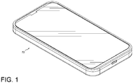
- Fig. 1 and FIG. 2 are diagrams showing a communication device 10 according to an embodiment of the present invention.
- the communication device 10 comprises a metal frame 12, a display module 14, a display panel 16, a metal back cover 18, a printed circuited board 20, and a main body 22.
- the metal frame 12 substantially is a rectangular frame defining an opening 24, and can be utilized as a front cover of the communication device 10.
- the display module 14 and the display panel 16 can be separated from each other or integrated together, but the present invention is not limited to the above structure.
- the display panel 16 is installed between the display module 14 and the metal frame 12, and corresponding to the opening 24 of the metal frame 12.
- the display panel 16 is made of glass, but not limited to it.
- the metal back cover 18 is substantially rectangular and located at a position corresponding to a bottom of the main body 22, for being utilized as a rear cover of the communication device 10.
- the printed circuit board 20 is located between the metal frame 12 and the metal back cover 18.
- the printed circuit board 20 comprises a first circuit block 26 and a second circuit block 28 electrically connected to the first circuit block 26.
- the main body 22 is located between the metal frame 12 and the metal back cover 18, for installing the display module 14, the display panel 16 and the printed circuited board 20 on the main body 22.
- the main body 22 is made of a non-conductive material, such as a plastic material, but not limited to it.
- FIG. 3 is a diagram showing arrangement of an antenna of the communication device according to an embodiment of the present invention.
- FIG. 4 to FIG. 6 are diagrams showing antenna arrangement of the communication device 10 supporting a first communication function, such as a global positioning system (GPS) function.
- the arrangement in FIG. 4 to FIG. 6 comprises the metal frame 12, the first circuit block 26 of the printed circuit board 20, a first conductor 30, a second conductor 32 and the metal back cover 18.
- the metal frame 12 has a first part 34 and a second part 36 located at a position different from a position of the first part 34.
- the first part 34 and the second part 36 of the metal frame 12 are located close to an upper right position of the display panel 16.
- the first circuit block 26 of the printed circuit board 20 comprises a signal terminal 38 and a ground terminal 40.
- the first conductor 30 is connected between the first part 34 of the metal frame 12 and the signal terminal 38 of the first circuit block 26 of the print circuit board 20.
- the second conductor 32 is connected between the second part 36 of the metal frame 12 and the ground terminal 40 of the first circuit block 26 of the print circuit board 20.
- FIG. 7 to FIG. 10 are diagrams showing antenna arrangement of the communication device 10 supporting a second communication function, such as a global system for mobile communication (GSM) function.
- the arrangement in FIG. 7 to FIG. 10 utilizes the metal frame 12 as a common antenna, wherein the arrangement comprises the second circuit block 28 of the printed circuit board 20, a third conductor 42, a fourth conductor 44 and a signal line 46.
- the second circuit block 28 of the printed circuit board 20 comprises a signal terminal 48 and a ground terminal 50.
- the metal frame 12 further has a third part 52 and a fourth part 54 located at a position different from a position of the third part 52. In a preferred embodiment, the third part 52 and the fourth part 54 of the metal frame 12 are located close to a lower right position of the display panel 16.
- the third conductor 42 is connected to the third part 52 of the metal frame 12, and extended in length to be close to the second circuit block 28 of the printed circuit board 20.
- the fourth conductor 44 is connected to a ground surface of the second circuit block 28 of the print circuit board 20 for conducting to the ground terminal 50, and at least one coupling gap 56 is defined between the third conductor 42 and the fourth conductor 44.
- the signal terminal 48 of the second circuit block 28 of the printed circuit board 20 is electrically connected to the fourth part 54 of the metal frame 12.
- the signal terminal 48 of the second circuit block 28 of the printed circuit board 20 can be electrically connected to the fourth part 54 of the metal frame 12 through the signal line 46 connecting or contacting the fourth part 54 of the metal frame 12; or, in another embodiment, the signal terminal 48 of the second circuit block 28 of the printed circuit board 20 can directly connect or contact the fourth part 54 of the metal frame 12, the present invention is not limited to the above.
- the metal back cover 18 contacts the ground terminal 50 of the second circuit block 28 of the printed circuit board 20.
- the metal frame 12 can work as a common antenna for the first communication function (GPS) and the second communication function (GSM).
- the antenna forms an approximate large loop antenna to cooperate with the first conductor 30 and the second conductor 32 forming a small loop antenna smaller than the metal frame 12, in order to provide required communication capability to the communication device 10 through calculation processing of the printed circuit board 20.
- the third conductor 42 and the fourth conductor 44 are pre-arranged to form an open circuit state through the at least one coupling gap 56, so as to adjust required antenna matching, such as impedance matching, according to requirement.
- the signal terminal 48 of the second circuit block 28 of the printed circuit board 20 is coupled to the ground surface and the ground terminal 50 of the second circuit block 28 of the printed circuit board 20 for grounding through the at least one coupling gap 56, and the ground terminal 50 contacts the metal back cover after assembling.
- the advantages of the present invention is that appearances of the metal back cover and the metal frame are not ruined by design of the antenna, and the present invention can have better appearance in contrast to the prior art, so as to allow the communication device to have great diversity of design.
Landscapes
- Engineering & Computer Science (AREA)
- Computer Networks & Wireless Communication (AREA)
- Support Of Aerials (AREA)
- Telephone Set Structure (AREA)
Claims (4)
- Kommunikationsgerät (10), welches umfasst:einen Metallrahmen (12), der eine Öffnung (24) definiert, worin der Metallrahmen (12) aufweist, ein erstes Teil (34), ein zweites Teil (36), das in Bezug zu dem ersten Teil (34) gebogen ist, ein drittes Teil (52) neben dem zweiten Teil (36), und ein viertes Teil (54), das in Bezug zu dem dritten Teil (52) gebogen und verschieden von dem ersten Teil ist;ein Anzeigemodul (14);ein Anzeigepaneel (16), das zwischen dem Anzeigemodul (14) und dem Metallrahmen (12) installiert ist und der Öffnung (24) des Metallrahmens (12) entspricht;eine metallene Rückseitenabdeckung (18);eine Leiterplatte (20), die einen ersten Schaltkreisblock (26) und einen zweiten Schaltkreisblock (28), der elektrisch mit dem ersten Schaltkreisblock (26) gekoppelt ist, umfasst, worin der erste und der zweite Schaltkreisblock (26, 28) einen Signal-Anschluss (38, 48) und einen Erdungs-Anschluss (40, 50) umfasst, worin der Erdungs-Anschluss (40, 50) mit der metallenen Rückseitenabdeckung (18) in Kontakt steht;einen Hauptkörper (22), der zwischen dem Metallrahmen (12) und der metallenen Rückseitenabdeckung (18) angeordnet ist, worin der Hauptkörper (22) aus einem nicht-leitendem Material besteht;dadurch gekennzeichnet, dass:ein erster Leiter (30) zwischen dem ersten Teil (34) des Metallrahmens (12) und dem Signalanschluss (38) des ersten Schaltkreisblock (26) der Leiterplatte (20) verbunden ist;ein zweiter Leiter (32) zwischen dem zweiten Teil (36) des Metallrahmens (12) und den Erdungsanschluss (40) des ersten Schaltkreisblock (26) der Leiterplatte (20) verbunden ist;ein dritter Leiter (42) aufweist, einen ersten Bereich, der entlang des dritten Teils (52) angeordnet und mit dem dritten Teil (52) des Metallrahmens (12) verbunden ist, und einen zweiten Bereich, der sich von dem ersten Bereich entlang einer Längsrichtung des zweite Schaltkreisblock (28) erstreckt, worin die Längsrichtung entlang de Richtung des vierten Teils (54) definiert wird; undein vierter Leiter (44) entlang einer Längsrichtung des zweiten Schaltkreisblock (28) angeordnet und mit dem Erdungsanschluss (50) des zweiten Schaltkreisblock (28) der Leiterplatte (20) verbunden ist, worin mindestens ein Kupplungs-Spalt (56) zwischen dem zweiten Bereich des dritten Leiters (42) und dem vierten Leiter (44) definiert ist;worin der Signal-Anschluss (48) des zweiten Schaltkreisblock (28) der Leiterplatte (20) elektrisch mit dem vierten Teil (54) des Metallrahmens (12) verbunden ist.
- Kommunikationsgerät nach Anspruch 1, dadurch gekennzeichnet, dass das erste Teil (34) und das zweite Teil (36) des Metallrahmens (12) einer ersten Ecke des Anzeigepaneels (16) entspricht.
- Kommunikationsgerät nach Anspruch 2, dadurch gekennzeichnet, dass das dritte Teil (52) und das vierte Teil (54) des Metallrahmens (12) einer zweiten Ecke des Anzeigepaneels (16), die verschieden ist von der ersten Ecke entspricht.
- Kommunikationsgerät nach einem der Ansprüche 1-3, dadurch gekennzeichnet, dass der erste Leiter (30) entlang des ersten Teils (34) und des zweiten Teil (36) angeordnet ist, dass der zweite Leiter (32) entlang des zweiten Teils (36) angeordnet ist, worin the erste Leiter (30), der zweite Leiter (32), das erste Teil (34) und das zweite Teil (36) eine Schleifenantenne ausbilden.
Priority Applications (1)
| Application Number | Priority Date | Filing Date | Title |
|---|---|---|---|
| EP14190198.3A EP3012904B1 (de) | 2014-10-24 | 2014-10-24 | Kommunikationsvorrichtung und Antenne dafür |
Applications Claiming Priority (1)
| Application Number | Priority Date | Filing Date | Title |
|---|---|---|---|
| EP14190198.3A EP3012904B1 (de) | 2014-10-24 | 2014-10-24 | Kommunikationsvorrichtung und Antenne dafür |
Publications (2)
| Publication Number | Publication Date |
|---|---|
| EP3012904A1 EP3012904A1 (de) | 2016-04-27 |
| EP3012904B1 true EP3012904B1 (de) | 2019-05-08 |
Family
ID=51794778
Family Applications (1)
| Application Number | Title | Priority Date | Filing Date |
|---|---|---|---|
| EP14190198.3A Active EP3012904B1 (de) | 2014-10-24 | 2014-10-24 | Kommunikationsvorrichtung und Antenne dafür |
Country Status (1)
| Country | Link |
|---|---|
| EP (1) | EP3012904B1 (de) |
Families Citing this family (3)
| Publication number | Priority date | Publication date | Assignee | Title |
|---|---|---|---|---|
| CN108232428A (zh) * | 2018-01-03 | 2018-06-29 | 上海传英信息技术有限公司 | 移动终端及其天线设置方法 |
| CN110767987A (zh) * | 2018-07-27 | 2020-02-07 | 深圳富泰宏精密工业有限公司 | 天线结构及具有该天线结构的无线通信装置 |
| CN119108790A (zh) * | 2023-06-08 | 2024-12-10 | Oppo广东移动通信有限公司 | 电子设备 |
Family Cites Families (4)
| Publication number | Priority date | Publication date | Assignee | Title |
|---|---|---|---|---|
| KR101501921B1 (ko) | 2008-05-06 | 2015-03-13 | 삼성전자주식회사 | 금속 케이스를 갖는 휴대 단말기 및 그의 안테나 구조 |
| US9041606B2 (en) * | 2011-11-30 | 2015-05-26 | Motorola Solutions, Inc. | Uninterrupted bezel antenna |
| US9203456B2 (en) * | 2012-09-25 | 2015-12-01 | Htc Corporation | Mobile device |
| US9142879B2 (en) * | 2012-11-13 | 2015-09-22 | Sony Corporation | Wireless electronic devices with a metal perimeter including a plurality of antennas |
-
2014
- 2014-10-24 EP EP14190198.3A patent/EP3012904B1/de active Active
Non-Patent Citations (1)
| Title |
|---|
| None * |
Also Published As
| Publication number | Publication date |
|---|---|
| EP3012904A1 (de) | 2016-04-27 |
Similar Documents
| Publication | Publication Date | Title |
|---|---|---|
| US9343802B2 (en) | Communication device and antenna thereof | |
| US9203141B1 (en) | Communication device and antenna thereof | |
| US10403966B2 (en) | Communication device and antenna assembly thereof | |
| US9331391B2 (en) | Mobile device | |
| KR101606145B1 (ko) | 휴대용 단말기의 안테나 장치 | |
| EP3012908B1 (de) | Mobiles endgerät mit neuartiger antennenstruktur | |
| US20150303551A1 (en) | Communication device antenna | |
| KR101600268B1 (ko) | 모바일 전자 장치 | |
| US8358777B2 (en) | Wireless telephone having support with built-in antenna | |
| EP3012904B1 (de) | Kommunikationsvorrichtung und Antenne dafür | |
| US10122069B2 (en) | Mobile terminal device | |
| CN108321492B (zh) | 电子设备 | |
| US10468749B2 (en) | Mobile display terminal | |
| JP2015043572A (ja) | アンテナ及びアンテナを備えた無線通信装置 | |
| EP2958189B1 (de) | Kommunikationsvorrichtung und Antenne dafür | |
| US9331379B2 (en) | Mobile device and manufacturing method thereof | |
| US20150303550A1 (en) | Communication device antenna | |
| ZA202401428B (en) | Electronic device comprising antenna | |
| US20150303552A1 (en) | Communication device antenna | |
| US20130093631A1 (en) | Mobile wireless terminal | |
| JP3195354U (ja) | 通信機器及び通信機器のアンテナ | |
| JP2012227743A (ja) | 携帯無線機 | |
| EP3343694B1 (de) | Antennenvorrichtung für mobiles endgerät sowie mobiles endgerät | |
| CN105514570B (zh) | 通讯装置及其天线 | |
| JP3193046U (ja) | 通信装置及び通信装置のアンテナ |
Legal Events
| Date | Code | Title | Description |
|---|---|---|---|
| PUAI | Public reference made under article 153(3) epc to a published international application that has entered the european phase |
Free format text: ORIGINAL CODE: 0009012 |
|
| AK | Designated contracting states |
Kind code of ref document: A1 Designated state(s): AL AT BE BG CH CY CZ DE DK EE ES FI FR GB GR HR HU IE IS IT LI LT LU LV MC MK MT NL NO PL PT RO RS SE SI SK SM TR |
|
| AX | Request for extension of the european patent |
Extension state: BA ME |
|
| 17P | Request for examination filed |
Effective date: 20160513 |
|
| RBV | Designated contracting states (corrected) |
Designated state(s): AL AT BE BG CH CY CZ DE DK EE ES FI FR GB GR HR HU IE IS IT LI LT LU LV MC MK MT NL NO PL PT RO RS SE SI SK SM TR |
|
| GRAP | Despatch of communication of intention to grant a patent |
Free format text: ORIGINAL CODE: EPIDOSNIGR1 |
|
| STAA | Information on the status of an ep patent application or granted ep patent |
Free format text: STATUS: GRANT OF PATENT IS INTENDED |
|
| INTG | Intention to grant announced |
Effective date: 20181211 |
|
| RIN1 | Information on inventor provided before grant (corrected) |
Inventor name: LIN, SHU-CHEN Inventor name: LIU, CHUN-TA Inventor name: SU, HSIN-CHENG |
|
| GRAS | Grant fee paid |
Free format text: ORIGINAL CODE: EPIDOSNIGR3 |
|
| GRAA | (expected) grant |
Free format text: ORIGINAL CODE: 0009210 |
|
| STAA | Information on the status of an ep patent application or granted ep patent |
Free format text: STATUS: THE PATENT HAS BEEN GRANTED |
|
| AK | Designated contracting states |
Kind code of ref document: B1 Designated state(s): AL AT BE BG CH CY CZ DE DK EE ES FI FR GB GR HR HU IE IS IT LI LT LU LV MC MK MT NL NO PL PT RO RS SE SI SK SM TR |
|
| REG | Reference to a national code |
Ref country code: GB Ref legal event code: FG4D |
|
| REG | Reference to a national code |
Ref country code: CH Ref legal event code: EP Ref country code: AT Ref legal event code: REF Ref document number: 1131677 Country of ref document: AT Kind code of ref document: T Effective date: 20190515 |
|
| REG | Reference to a national code |
Ref country code: DE Ref legal event code: R096 Ref document number: 602014046175 Country of ref document: DE Ref country code: IE Ref legal event code: FG4D |
|
| REG | Reference to a national code |
Ref country code: NL Ref legal event code: MP Effective date: 20190508 |
|
| REG | Reference to a national code |
Ref country code: LT Ref legal event code: MG4D |
|
| PG25 | Lapsed in a contracting state [announced via postgrant information from national office to epo] |
Ref country code: NO Free format text: LAPSE BECAUSE OF FAILURE TO SUBMIT A TRANSLATION OF THE DESCRIPTION OR TO PAY THE FEE WITHIN THE PRESCRIBED TIME-LIMIT Effective date: 20190808 Ref country code: HR Free format text: LAPSE BECAUSE OF FAILURE TO SUBMIT A TRANSLATION OF THE DESCRIPTION OR TO PAY THE FEE WITHIN THE PRESCRIBED TIME-LIMIT Effective date: 20190508 Ref country code: SE Free format text: LAPSE BECAUSE OF FAILURE TO SUBMIT A TRANSLATION OF THE DESCRIPTION OR TO PAY THE FEE WITHIN THE PRESCRIBED TIME-LIMIT Effective date: 20190508 Ref country code: FI Free format text: LAPSE BECAUSE OF FAILURE TO SUBMIT A TRANSLATION OF THE DESCRIPTION OR TO PAY THE FEE WITHIN THE PRESCRIBED TIME-LIMIT Effective date: 20190508 Ref country code: PT Free format text: LAPSE BECAUSE OF FAILURE TO SUBMIT A TRANSLATION OF THE DESCRIPTION OR TO PAY THE FEE WITHIN THE PRESCRIBED TIME-LIMIT Effective date: 20190908 Ref country code: AL Free format text: LAPSE BECAUSE OF FAILURE TO SUBMIT A TRANSLATION OF THE DESCRIPTION OR TO PAY THE FEE WITHIN THE PRESCRIBED TIME-LIMIT Effective date: 20190508 Ref country code: ES Free format text: LAPSE BECAUSE OF FAILURE TO SUBMIT A TRANSLATION OF THE DESCRIPTION OR TO PAY THE FEE WITHIN THE PRESCRIBED TIME-LIMIT Effective date: 20190508 Ref country code: NL Free format text: LAPSE BECAUSE OF FAILURE TO SUBMIT A TRANSLATION OF THE DESCRIPTION OR TO PAY THE FEE WITHIN THE PRESCRIBED TIME-LIMIT Effective date: 20190508 Ref country code: LT Free format text: LAPSE BECAUSE OF FAILURE TO SUBMIT A TRANSLATION OF THE DESCRIPTION OR TO PAY THE FEE WITHIN THE PRESCRIBED TIME-LIMIT Effective date: 20190508 |
|
| PG25 | Lapsed in a contracting state [announced via postgrant information from national office to epo] |
Ref country code: BG Free format text: LAPSE BECAUSE OF FAILURE TO SUBMIT A TRANSLATION OF THE DESCRIPTION OR TO PAY THE FEE WITHIN THE PRESCRIBED TIME-LIMIT Effective date: 20190808 Ref country code: LV Free format text: LAPSE BECAUSE OF FAILURE TO SUBMIT A TRANSLATION OF THE DESCRIPTION OR TO PAY THE FEE WITHIN THE PRESCRIBED TIME-LIMIT Effective date: 20190508 Ref country code: RS Free format text: LAPSE BECAUSE OF FAILURE TO SUBMIT A TRANSLATION OF THE DESCRIPTION OR TO PAY THE FEE WITHIN THE PRESCRIBED TIME-LIMIT Effective date: 20190508 Ref country code: GR Free format text: LAPSE BECAUSE OF FAILURE TO SUBMIT A TRANSLATION OF THE DESCRIPTION OR TO PAY THE FEE WITHIN THE PRESCRIBED TIME-LIMIT Effective date: 20190809 |
|
| REG | Reference to a national code |
Ref country code: AT Ref legal event code: MK05 Ref document number: 1131677 Country of ref document: AT Kind code of ref document: T Effective date: 20190508 |
|
| REG | Reference to a national code |
Ref country code: DE Ref legal event code: R082 Ref document number: 602014046175 Country of ref document: DE Representative=s name: STRAUS, ALEXANDER, DIPL.-CHEM.UNIV. DR.PHIL., DE Ref country code: DE Ref legal event code: R082 Ref document number: 602014046175 Country of ref document: DE Representative=s name: 2K PATENT- UND RECHTSANWAELTE PARTNERSCHAFT MB, DE |
|
| PG25 | Lapsed in a contracting state [announced via postgrant information from national office to epo] |
Ref country code: RO Free format text: LAPSE BECAUSE OF FAILURE TO SUBMIT A TRANSLATION OF THE DESCRIPTION OR TO PAY THE FEE WITHIN THE PRESCRIBED TIME-LIMIT Effective date: 20190508 Ref country code: SK Free format text: LAPSE BECAUSE OF FAILURE TO SUBMIT A TRANSLATION OF THE DESCRIPTION OR TO PAY THE FEE WITHIN THE PRESCRIBED TIME-LIMIT Effective date: 20190508 Ref country code: AT Free format text: LAPSE BECAUSE OF FAILURE TO SUBMIT A TRANSLATION OF THE DESCRIPTION OR TO PAY THE FEE WITHIN THE PRESCRIBED TIME-LIMIT Effective date: 20190508 Ref country code: EE Free format text: LAPSE BECAUSE OF FAILURE TO SUBMIT A TRANSLATION OF THE DESCRIPTION OR TO PAY THE FEE WITHIN THE PRESCRIBED TIME-LIMIT Effective date: 20190508 Ref country code: DK Free format text: LAPSE BECAUSE OF FAILURE TO SUBMIT A TRANSLATION OF THE DESCRIPTION OR TO PAY THE FEE WITHIN THE PRESCRIBED TIME-LIMIT Effective date: 20190508 Ref country code: CZ Free format text: LAPSE BECAUSE OF FAILURE TO SUBMIT A TRANSLATION OF THE DESCRIPTION OR TO PAY THE FEE WITHIN THE PRESCRIBED TIME-LIMIT Effective date: 20190508 |
|
| REG | Reference to a national code |
Ref country code: DE Ref legal event code: R097 Ref document number: 602014046175 Country of ref document: DE |
|
| PG25 | Lapsed in a contracting state [announced via postgrant information from national office to epo] |
Ref country code: SM Free format text: LAPSE BECAUSE OF FAILURE TO SUBMIT A TRANSLATION OF THE DESCRIPTION OR TO PAY THE FEE WITHIN THE PRESCRIBED TIME-LIMIT Effective date: 20190508 Ref country code: IT Free format text: LAPSE BECAUSE OF FAILURE TO SUBMIT A TRANSLATION OF THE DESCRIPTION OR TO PAY THE FEE WITHIN THE PRESCRIBED TIME-LIMIT Effective date: 20190508 |
|
| PLBE | No opposition filed within time limit |
Free format text: ORIGINAL CODE: 0009261 |
|
| STAA | Information on the status of an ep patent application or granted ep patent |
Free format text: STATUS: NO OPPOSITION FILED WITHIN TIME LIMIT |
|
| PG25 | Lapsed in a contracting state [announced via postgrant information from national office to epo] |
Ref country code: TR Free format text: LAPSE BECAUSE OF FAILURE TO SUBMIT A TRANSLATION OF THE DESCRIPTION OR TO PAY THE FEE WITHIN THE PRESCRIBED TIME-LIMIT Effective date: 20190508 |
|
| 26N | No opposition filed |
Effective date: 20200211 |
|
| PG25 | Lapsed in a contracting state [announced via postgrant information from national office to epo] |
Ref country code: PL Free format text: LAPSE BECAUSE OF FAILURE TO SUBMIT A TRANSLATION OF THE DESCRIPTION OR TO PAY THE FEE WITHIN THE PRESCRIBED TIME-LIMIT Effective date: 20190508 |
|
| PG25 | Lapsed in a contracting state [announced via postgrant information from national office to epo] |
Ref country code: SI Free format text: LAPSE BECAUSE OF FAILURE TO SUBMIT A TRANSLATION OF THE DESCRIPTION OR TO PAY THE FEE WITHIN THE PRESCRIBED TIME-LIMIT Effective date: 20190508 Ref country code: MC Free format text: LAPSE BECAUSE OF FAILURE TO SUBMIT A TRANSLATION OF THE DESCRIPTION OR TO PAY THE FEE WITHIN THE PRESCRIBED TIME-LIMIT Effective date: 20190508 |
|
| REG | Reference to a national code |
Ref country code: CH Ref legal event code: PL |
|
| PG25 | Lapsed in a contracting state [announced via postgrant information from national office to epo] |
Ref country code: LI Free format text: LAPSE BECAUSE OF NON-PAYMENT OF DUE FEES Effective date: 20191031 Ref country code: CH Free format text: LAPSE BECAUSE OF NON-PAYMENT OF DUE FEES Effective date: 20191031 Ref country code: LU Free format text: LAPSE BECAUSE OF NON-PAYMENT OF DUE FEES Effective date: 20191024 |
|
| REG | Reference to a national code |
Ref country code: BE Ref legal event code: MM Effective date: 20191031 |
|
| PG25 | Lapsed in a contracting state [announced via postgrant information from national office to epo] |
Ref country code: BE Free format text: LAPSE BECAUSE OF NON-PAYMENT OF DUE FEES Effective date: 20191031 |
|
| PG25 | Lapsed in a contracting state [announced via postgrant information from national office to epo] |
Ref country code: IE Free format text: LAPSE BECAUSE OF NON-PAYMENT OF DUE FEES Effective date: 20191024 Ref country code: FR Free format text: LAPSE BECAUSE OF NON-PAYMENT OF DUE FEES Effective date: 20191031 |
|
| PG25 | Lapsed in a contracting state [announced via postgrant information from national office to epo] |
Ref country code: CY Free format text: LAPSE BECAUSE OF FAILURE TO SUBMIT A TRANSLATION OF THE DESCRIPTION OR TO PAY THE FEE WITHIN THE PRESCRIBED TIME-LIMIT Effective date: 20190508 |
|
| PG25 | Lapsed in a contracting state [announced via postgrant information from national office to epo] |
Ref country code: IS Free format text: LAPSE BECAUSE OF FAILURE TO SUBMIT A TRANSLATION OF THE DESCRIPTION OR TO PAY THE FEE WITHIN THE PRESCRIBED TIME-LIMIT Effective date: 20190908 |
|
| PG25 | Lapsed in a contracting state [announced via postgrant information from national office to epo] |
Ref country code: MT Free format text: LAPSE BECAUSE OF FAILURE TO SUBMIT A TRANSLATION OF THE DESCRIPTION OR TO PAY THE FEE WITHIN THE PRESCRIBED TIME-LIMIT Effective date: 20190508 Ref country code: HU Free format text: LAPSE BECAUSE OF FAILURE TO SUBMIT A TRANSLATION OF THE DESCRIPTION OR TO PAY THE FEE WITHIN THE PRESCRIBED TIME-LIMIT; INVALID AB INITIO Effective date: 20141024 |
|
| PG25 | Lapsed in a contracting state [announced via postgrant information from national office to epo] |
Ref country code: MK Free format text: LAPSE BECAUSE OF FAILURE TO SUBMIT A TRANSLATION OF THE DESCRIPTION OR TO PAY THE FEE WITHIN THE PRESCRIBED TIME-LIMIT Effective date: 20190508 |
|
| REG | Reference to a national code |
Ref country code: DE Ref legal event code: R082 Ref document number: 602014046175 Country of ref document: DE Representative=s name: STRAUS, ALEXANDER, DIPL.-CHEM.UNIV. DR.PHIL., DE |
|
| PGFP | Annual fee paid to national office [announced via postgrant information from national office to epo] |
Ref country code: GB Payment date: 20250805 Year of fee payment: 12 |
|
| PGFP | Annual fee paid to national office [announced via postgrant information from national office to epo] |
Ref country code: DE Payment date: 20250611 Year of fee payment: 12 |