EP3012954A2 - Magnetisierungs-ausgleichsverfahren - Google Patents
Magnetisierungs-ausgleichsverfahren Download PDFInfo
- Publication number
- EP3012954A2 EP3012954A2 EP15191295.3A EP15191295A EP3012954A2 EP 3012954 A2 EP3012954 A2 EP 3012954A2 EP 15191295 A EP15191295 A EP 15191295A EP 3012954 A2 EP3012954 A2 EP 3012954A2
- Authority
- EP
- European Patent Office
- Prior art keywords
- mosfet
- gate
- time
- power supply
- magnetization
- Prior art date
- Legal status (The legal status is an assumption and is not a legal conclusion. Google has not performed a legal analysis and makes no representation as to the accuracy of the status listed.)
- Granted
Links
- 238000000034 method Methods 0.000 title claims abstract description 21
- 230000005415 magnetization Effects 0.000 title claims abstract description 20
- 238000005516 engineering process Methods 0.000 description 11
- 241000699670 Mus sp. Species 0.000 description 1
- 238000003491 array Methods 0.000 description 1
- 239000003990 capacitor Substances 0.000 description 1
- 239000000969 carrier Substances 0.000 description 1
- 238000004891 communication Methods 0.000 description 1
- 230000008878 coupling Effects 0.000 description 1
- 238000010168 coupling process Methods 0.000 description 1
- 238000005859 coupling reaction Methods 0.000 description 1
- 230000005669 field effect Effects 0.000 description 1
- 230000014509 gene expression Effects 0.000 description 1
- 230000010354 integration Effects 0.000 description 1
- 230000003993 interaction Effects 0.000 description 1
- 239000000463 material Substances 0.000 description 1
- 238000012986 modification Methods 0.000 description 1
- 230000004048 modification Effects 0.000 description 1
- 230000003287 optical effect Effects 0.000 description 1
- 239000004065 semiconductor Substances 0.000 description 1
Images



Classifications
-
- H—ELECTRICITY
- H02—GENERATION; CONVERSION OR DISTRIBUTION OF ELECTRIC POWER
- H02M—APPARATUS FOR CONVERSION BETWEEN AC AND AC, BETWEEN AC AND DC, OR BETWEEN DC AND DC, AND FOR USE WITH MAINS OR SIMILAR POWER SUPPLY SYSTEMS; CONVERSION OF DC OR AC INPUT POWER INTO SURGE OUTPUT POWER; CONTROL OR REGULATION THEREOF
- H02M3/00—Conversion of DC power input into DC power output
- H02M3/22—Conversion of DC power input into DC power output with intermediate conversion into AC
- H02M3/24—Conversion of DC power input into DC power output with intermediate conversion into AC by static converters
- H02M3/28—Conversion of DC power input into DC power output with intermediate conversion into AC by static converters using discharge tubes with control electrode or semiconductor devices with control electrode to produce the intermediate AC
- H02M3/325—Conversion of DC power input into DC power output with intermediate conversion into AC by static converters using discharge tubes with control electrode or semiconductor devices with control electrode to produce the intermediate AC using devices of a triode or a transistor type requiring continuous application of a control signal
- H02M3/335—Conversion of DC power input into DC power output with intermediate conversion into AC by static converters using discharge tubes with control electrode or semiconductor devices with control electrode to produce the intermediate AC using devices of a triode or a transistor type requiring continuous application of a control signal using semiconductor devices only
- H02M3/33507—Conversion of DC power input into DC power output with intermediate conversion into AC by static converters using discharge tubes with control electrode or semiconductor devices with control electrode to produce the intermediate AC using devices of a triode or a transistor type requiring continuous application of a control signal using semiconductor devices only with automatic control of the output voltage or current, e.g. flyback converters
-
- H—ELECTRICITY
- H02—GENERATION; CONVERSION OR DISTRIBUTION OF ELECTRIC POWER
- H02M—APPARATUS FOR CONVERSION BETWEEN AC AND AC, BETWEEN AC AND DC, OR BETWEEN DC AND DC, AND FOR USE WITH MAINS OR SIMILAR POWER SUPPLY SYSTEMS; CONVERSION OF DC OR AC INPUT POWER INTO SURGE OUTPUT POWER; CONTROL OR REGULATION THEREOF
- H02M1/00—Details of apparatus for conversion
- H02M1/40—Means for preventing magnetic saturation
-
- H—ELECTRICITY
- H02—GENERATION; CONVERSION OR DISTRIBUTION OF ELECTRIC POWER
- H02M—APPARATUS FOR CONVERSION BETWEEN AC AND AC, BETWEEN AC AND DC, OR BETWEEN DC AND DC, AND FOR USE WITH MAINS OR SIMILAR POWER SUPPLY SYSTEMS; CONVERSION OF DC OR AC INPUT POWER INTO SURGE OUTPUT POWER; CONTROL OR REGULATION THEREOF
- H02M3/00—Conversion of DC power input into DC power output
- H02M3/22—Conversion of DC power input into DC power output with intermediate conversion into AC
- H02M3/24—Conversion of DC power input into DC power output with intermediate conversion into AC by static converters
- H02M3/28—Conversion of DC power input into DC power output with intermediate conversion into AC by static converters using discharge tubes with control electrode or semiconductor devices with control electrode to produce the intermediate AC
- H02M3/325—Conversion of DC power input into DC power output with intermediate conversion into AC by static converters using discharge tubes with control electrode or semiconductor devices with control electrode to produce the intermediate AC using devices of a triode or a transistor type requiring continuous application of a control signal
- H02M3/335—Conversion of DC power input into DC power output with intermediate conversion into AC by static converters using discharge tubes with control electrode or semiconductor devices with control electrode to produce the intermediate AC using devices of a triode or a transistor type requiring continuous application of a control signal using semiconductor devices only
- H02M3/337—Conversion of DC power input into DC power output with intermediate conversion into AC by static converters using discharge tubes with control electrode or semiconductor devices with control electrode to produce the intermediate AC using devices of a triode or a transistor type requiring continuous application of a control signal using semiconductor devices only in push-pull configuration
- H02M3/3372—Conversion of DC power input into DC power output with intermediate conversion into AC by static converters using discharge tubes with control electrode or semiconductor devices with control electrode to produce the intermediate AC using devices of a triode or a transistor type requiring continuous application of a control signal using semiconductor devices only in push-pull configuration of the parallel type
Definitions
- This disclosure relates generally to switching power supplies and, more particularly, to techniques for magnetization balancing with regard to such power supplies.
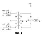
- FIGURE 1 illustrates an example of a typical push-pull switching power supply 100.
- the switching power supply 100 includes two metal-oxide-semiconductor field-effect transistor (MOSFETs) (here, MOSFET 1 and MOSFET 2) and an output voltage (V out ) at a load (Load).
- MOSFETs metal-oxide-semiconductor field-effect transistor
- V out output voltage
- the gate of MOSFET 1 (Gate 1) is driven with a square wave and the gate of MOSFET 2 (Gate 2) is driven with an inversion of the square wave driving Gate 1.
- FIGURE 2 is a graphical representation 200 of the gate voltages (V G1 and V G2 , respectively) and drain voltages (V D1 and V D2 , respectively) of MOSFET 1 and MOSFET 2 and magnetization current (e.g., the time integration of the voltage applied across the transformer) corresponding to the power supply 100 illustrated by FIGURE 1 .
- a common problem a power supply design such as the power supply 100 illustrated by FIGURE 1 occurs when there is a small difference in the volt-seconds that are applied during the on-time of MOSFET 1 versus the volt-seconds that are applied during the on-time of MOSFET 2.
- the magnetization current will generally develop a DC component that will build until the resistive losses force the volt-seconds to be balanced, at which time the DC component stop increasing. If the resistive losses are small, the transformer will saturate, thus resulting in large magnetizing currents than can destroy either or both MOSFETs.
- Embodiments of the disclosed technology generally pertain to techniques for magnetization balancing for switching power supplies.
- Implementations of the disclosed technology are generally directed to a balancing technique for switching power supplies.
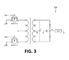
- FIGURE 3 illustrates an example of a push-pull switching power supply 300 in accordance with certain embodiments of the disclosed technology.
- the gate of MOSFET 1 (Gate 1) is driven with a less-than-50% on pulse and the gate of MOSFET 2 (Gate 2) is driven with a second, equal pulse that is phase-shifted 180 degrees.
- the magnetizing current will cause the voltage on the transformer to commutate (i.e., flip voltage).
- capacitor C Adding capacitance across the transformer allows the commutation slew rate to be slowed down/controlled. If the volt-seconds are not balanced, the magnetizing current will typically take on a DC component. This DC component will generally cause the one phase to commutate faster and the other to commutate slower. This will shift the volt-second mismatch toward a balance and stop the DC component from continuing to increase. If the gate drives have slow rise and fall times, the starting volt-second mismatch can be significant due to the variation of MOSFET threshold voltage. The result is generally a large difference between the commutation times.
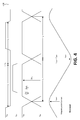
- FIGURE 4 is a first graphical representation 400 of the MOSFET gate voltages and drain voltages as well as the magnetization current corresponding to a power supply, such as the push-pull switching power supply 300 illustrated by FIGURE 3 , in accordance with certain embodiments of the disclosed technology.
- the gate drive has an off time between each on time to allow time for the magnetization current to commutate the drains.
- FIGURE 5 is a second graphical representation 500 of the MOSFET gate voltages and drain voltages as well as the magnetization current corresponding to a power supply, such as the push-pull switching power supply 300 illustrated by FIGURE 3 , in accordance with certain embodiments of the disclosed technology.
- the gate drive has an off time between each on time to allow time for the magnetization current to commutate the drains.
- the commutation times (t 1 and t 2 ) are not balanced (e.g., t 1 ⁇ t 2 ).
- FIGURE 6 illustrates an example of a method 600 of magnetization balancing for a switching power supply, such as the push-pull switching power supply 300 illustrated by FIGURE 3 , in accordance with certain embodiments of the disclosed technology.
- the commutation time of the two phases corresponding to a power supply having two MOSFETs is measured.
- the gate of a first MOSFET will be referred to as Gate 1 and the gate of a second MOSFET will be referred to as Gate 2.
- the timing (e.g., phase) of the on time (pulse width) of Gate 1 relative to the on time (pulse width) of Gate 2 is adjusted (e.g., incremented) in order to balance the volt-second of the two phases.
- machine is intended to broadly encompass a single machine or a system of communicatively coupled machines or devices operating together.
- Exemplary machines may include computing devices such as personal computers, workstations, servers, portable computers, handheld devices, tablet devices, and the like.
- a machine typically includes a system bus to which processors, memory such as random access memory (RAM), read-only memory (ROM), and other state-preserving medium, storage devices, a video interface, and input/output interface ports can be attached.
- the machine may also include embedded controllers such as programmable or non-programmable logic devices or arrays, Application Specific Integrated Circuits (ASICs), embedded computers, smart cards, and the like.
- the machine may be controlled, at least in part, by input from conventional input devices such as keyboards and mice, as well as by directives received from another machine, interaction with a virtual reality (VR) environment, biometric feedback, or other pertinent input.
- VR virtual reality
- the machine may utilize one or more connections to one or more remote machines, such as through a network interface, modem, or other communicative coupling.
- Machines can be interconnected by way of a physical and/or logical network, such as an intranet, the Internet, local area networks, wide area networks, etc.
- network communication may utilize various wired and/or wireless short range or long range carriers and protocols, including radio frequency (RF), satellite, microwave, Institute of Electrical and Electronics Engineers (IEEE) 545.11, Bluetooth, optical, infrared, cable, laser, etc.
- RF radio frequency
- IEEE Institute of Electrical and Electronics Engineers
- Examples provide a method of magnetization balancing for a switching power supply of a type where the magnetization drives the commutations of the switching, the switching power supply having a first MOSFET and a second MOSFET, the first MOSFET having a gate and the second MOSFET having a gate, the method comprising measuring a first commutation time, measuring a second commutation time adjusting a timing of an on time (pulse width) of the gate of the first MOSFET relative to an on time (pulse width) of the gate of the second MOSFET, and determining whether the first commutation time is at least substantially equal to the second commutation time.
- the method further comprises again adjusting the timing of the on time (pulse width) of the gate of the first MOSFET relative to the on time (pulse width) of the gate of the second MOSFET responsive to a determination that the first commutation time is not at least substantially equal to the second commutation time.
- the method further comprises stopping the method responsive to a determination that the first commutation time is at least substantially equal to the second commutation time.
- Examples provide a switching power supply operable to carry out any of the disclosed methods.
Landscapes
- Engineering & Computer Science (AREA)
- Power Engineering (AREA)
- Dc-Dc Converters (AREA)
- Power Conversion In General (AREA)
- Electronic Switches (AREA)
Applications Claiming Priority (1)
| Application Number | Priority Date | Filing Date | Title |
|---|---|---|---|
| US14/523,745 US20160118899A1 (en) | 2014-10-24 | 2014-10-24 | Magnetization balancing method |
Publications (3)
| Publication Number | Publication Date |
|---|---|
| EP3012954A2 true EP3012954A2 (de) | 2016-04-27 |
| EP3012954A3 EP3012954A3 (de) | 2016-06-29 |
| EP3012954B1 EP3012954B1 (de) | 2017-08-16 |
Family
ID=54360177
Family Applications (1)
| Application Number | Title | Priority Date | Filing Date |
|---|---|---|---|
| EP15191295.3A Not-in-force EP3012954B1 (de) | 2014-10-24 | 2015-10-23 | Magnetisierungs-ausgleichsverfahren |
Country Status (5)
| Country | Link |
|---|---|
| US (1) | US20160118899A1 (de) |
| EP (1) | EP3012954B1 (de) |
| JP (1) | JP2016086637A (de) |
| CN (1) | CN105553285A (de) |
| TW (1) | TW201628327A (de) |
Cited By (1)
| Publication number | Priority date | Publication date | Assignee | Title |
|---|---|---|---|---|
| EP4633019A1 (de) * | 2024-03-28 | 2025-10-15 | Lian Zheng Electronic (Shenzhen) Co., Ltd. | Gegentakttransformator, gleichspannungswandler und unterbrechungsfreie stromversorgung |
Families Citing this family (4)
| Publication number | Priority date | Publication date | Assignee | Title |
|---|---|---|---|---|
| US9991778B2 (en) * | 2016-02-29 | 2018-06-05 | The Boeing Company | Balancing current within a modular converter system |
| US10892649B2 (en) * | 2016-10-18 | 2021-01-12 | Etherdyne Technologies Inc. | Radio frequency (RF) power source and method for use with a wireless power transmitter of a wireless power transfer system |
| US10250078B2 (en) | 2016-10-18 | 2019-04-02 | Robert A Moffatt | Wireless power transfer to multiple receiver devices across a variable-sized area |
| TWI620403B (zh) * | 2017-03-09 | 2018-04-01 | Improved self-excited push-pull type conversion circuit |
Family Cites Families (8)
| Publication number | Priority date | Publication date | Assignee | Title |
|---|---|---|---|---|
| US4553198A (en) * | 1982-12-10 | 1985-11-12 | Powercube Corporation | Power converter symmetry correction circuit |
| EP0261663B1 (de) * | 1986-09-26 | 1992-06-17 | Hitachi, Ltd. | Laservorrichtung mit Hochspannungsimpulsgenerator, Hochspannungsimpulsgenerator und Verfahren zur Impulserzeugung |
| JP2004015900A (ja) * | 2002-06-05 | 2004-01-15 | Omron Corp | プッシュプル回路方式の電力変換装置 |
| EP2515426B1 (de) * | 2011-04-20 | 2019-06-12 | Nxp B.V. | Schaltkreis |
| US8891269B2 (en) * | 2011-10-10 | 2014-11-18 | Texas Instruments Incorporated | Full bridge converter |
| US9099932B2 (en) * | 2013-01-07 | 2015-08-04 | Analog Devices Global | Duty cycle balance module for switch mode power converter |
| CN103219890B (zh) * | 2013-03-29 | 2016-05-25 | 大洋电机新动力科技有限公司 | 一种igbt驱动模块的供电电源系统 |
| US9184655B2 (en) * | 2014-03-17 | 2015-11-10 | Semiconductor Components Industries, Llc | Method and semiconductor device for a dedicated startup sequence in a resonant converter |
-
2014
- 2014-10-24 US US14/523,745 patent/US20160118899A1/en not_active Abandoned
-
2015
- 2015-07-27 TW TW104124260A patent/TW201628327A/zh unknown
- 2015-10-23 EP EP15191295.3A patent/EP3012954B1/de not_active Not-in-force
- 2015-10-23 CN CN201510691049.0A patent/CN105553285A/zh active Pending
- 2015-10-26 JP JP2015210024A patent/JP2016086637A/ja active Pending
Non-Patent Citations (1)
| Title |
|---|
| None |
Cited By (1)
| Publication number | Priority date | Publication date | Assignee | Title |
|---|---|---|---|---|
| EP4633019A1 (de) * | 2024-03-28 | 2025-10-15 | Lian Zheng Electronic (Shenzhen) Co., Ltd. | Gegentakttransformator, gleichspannungswandler und unterbrechungsfreie stromversorgung |
Also Published As
| Publication number | Publication date |
|---|---|
| TW201628327A (zh) | 2016-08-01 |
| EP3012954B1 (de) | 2017-08-16 |
| EP3012954A3 (de) | 2016-06-29 |
| JP2016086637A (ja) | 2016-05-19 |
| US20160118899A1 (en) | 2016-04-28 |
| CN105553285A (zh) | 2016-05-04 |
Similar Documents
| Publication | Publication Date | Title |
|---|---|---|
| EP3012954A2 (de) | Magnetisierungs-ausgleichsverfahren | |
| US9735771B1 (en) | Hybrid switch including GaN HEMT and MOSFET | |
| EP3590189B1 (de) | Hybridschaltersteuerung | |
| CN119895719A (zh) | 用于针对用于电动车辆的逆变器的自适应栅极驱动器的系统和方法 | |
| US8797776B2 (en) | Diode-less full-wave rectifier for low-power on-chip AC-DC conversion | |
| EP2658106A1 (de) | Brückenlose leistungsfaktorkorrekturschaltung und steuerverfahren dafür | |
| CN105446923B (zh) | 具有上拉升压器和下拉升压器的差分驱动器 | |
| CN104850210B (zh) | 一种电源门控电路 | |
| US9496788B2 (en) | Multi-phase boost converter with phase self-detection and detecting circuit thereof | |
| TWI656734B (zh) | 用於控制高側切換元件之變化率之電路 | |
| CN101442284A (zh) | 马达驱动电路、风扇马达、电子设备及笔记本个人计算机 | |
| KR20170131452A (ko) | 파워 fet들의 캐스코드 스택용 드라이브 | |
| US8964436B2 (en) | Self-starting transistor-only full-wave rectifier for on-chip AC-DC conversion | |
| US10411687B2 (en) | Near zero quiescent current circuit for selecting a maximum supply voltage | |
| EP2992607B1 (de) | Lastumschalter | |
| US11309814B2 (en) | Electric motor power control circuitry | |
| US20160254700A1 (en) | Resonant type high frequency power supply device and switching circuit for resonant type high frequency power supply device | |
| CN108233682B (zh) | 驱动电路及驱动方法 | |
| US9935560B2 (en) | Electronic device with a maintain power signature (MPS) device and associated methods | |
| EP4447309A2 (de) | Leistungs-mosfet-treiberschaltung mit übertragungskurvengatetreiber und erdungsverschiebungskompensation | |
| EP3057236B1 (de) | Treiberschaltung für eine Einzeldrahtprotokoll-Slave-Einheit | |
| US11088609B2 (en) | Low noise power supply MOSFET gate drive scheme | |
| CN112655144A (zh) | 用于半导体器件的电压平衡电路 | |
| US20210273563A1 (en) | High energy pulse on a high-voltage-direct-current offset | |
| KR101440919B1 (ko) | Cmos 정류기 |
Legal Events
| Date | Code | Title | Description |
|---|---|---|---|
| PUAI | Public reference made under article 153(3) epc to a published international application that has entered the european phase |
Free format text: ORIGINAL CODE: 0009012 |
|
| AK | Designated contracting states |
Kind code of ref document: A2 Designated state(s): AL AT BE BG CH CY CZ DE DK EE ES FI FR GB GR HR HU IE IS IT LI LT LU LV MC MK MT NL NO PL PT RO RS SE SI SK SM TR |
|
| AX | Request for extension of the european patent |
Extension state: BA ME |
|
| PUAL | Search report despatched |
Free format text: ORIGINAL CODE: 0009013 |
|
| AK | Designated contracting states |
Kind code of ref document: A3 Designated state(s): AL AT BE BG CH CY CZ DE DK EE ES FI FR GB GR HR HU IE IS IT LI LT LU LV MC MK MT NL NO PL PT RO RS SE SI SK SM TR |
|
| AX | Request for extension of the european patent |
Extension state: BA ME |
|
| RIC1 | Information provided on ipc code assigned before grant |
Ipc: H02M 3/337 20060101ALI20160523BHEP Ipc: H02M 1/40 20070101AFI20160523BHEP |
|
| 17P | Request for examination filed |
Effective date: 20161221 |
|
| RBV | Designated contracting states (corrected) |
Designated state(s): AL AT BE BG CH CY CZ DE DK EE ES FI FR GB GR HR HU IE IS IT LI LT LU LV MC MK MT NL NO PL PT RO RS SE SI SK SM TR |
|
| GRAP | Despatch of communication of intention to grant a patent |
Free format text: ORIGINAL CODE: EPIDOSNIGR1 |
|
| INTG | Intention to grant announced |
Effective date: 20170412 |
|
| RIN1 | Information on inventor provided before grant (corrected) |
Inventor name: GOEKE, WAYNE |
|
| GRAS | Grant fee paid |
Free format text: ORIGINAL CODE: EPIDOSNIGR3 |
|
| GRAA | (expected) grant |
Free format text: ORIGINAL CODE: 0009210 |
|
| AK | Designated contracting states |
Kind code of ref document: B1 Designated state(s): AL AT BE BG CH CY CZ DE DK EE ES FI FR GB GR HR HU IE IS IT LI LT LU LV MC MK MT NL NO PL PT RO RS SE SI SK SM TR |
|
| REG | Reference to a national code |
Ref country code: GB Ref legal event code: FG4D |
|
| REG | Reference to a national code |
Ref country code: CH Ref legal event code: EP |
|
| REG | Reference to a national code |
Ref country code: IE Ref legal event code: FG4D |
|
| REG | Reference to a national code |
Ref country code: AT Ref legal event code: REF Ref document number: 919978 Country of ref document: AT Kind code of ref document: T Effective date: 20170915 |
|
| REG | Reference to a national code |
Ref country code: DE Ref legal event code: R096 Ref document number: 602015004137 Country of ref document: DE |
|
| REG | Reference to a national code |
Ref country code: NL Ref legal event code: MP Effective date: 20170816 |
|
| REG | Reference to a national code |
Ref country code: LT Ref legal event code: MG4D |
|
| REG | Reference to a national code |
Ref country code: AT Ref legal event code: MK05 Ref document number: 919978 Country of ref document: AT Kind code of ref document: T Effective date: 20170816 |
|
| PG25 | Lapsed in a contracting state [announced via postgrant information from national office to epo] |
Ref country code: SE Free format text: LAPSE BECAUSE OF FAILURE TO SUBMIT A TRANSLATION OF THE DESCRIPTION OR TO PAY THE FEE WITHIN THE PRESCRIBED TIME-LIMIT Effective date: 20170816 Ref country code: AT Free format text: LAPSE BECAUSE OF FAILURE TO SUBMIT A TRANSLATION OF THE DESCRIPTION OR TO PAY THE FEE WITHIN THE PRESCRIBED TIME-LIMIT Effective date: 20170816 Ref country code: LT Free format text: LAPSE BECAUSE OF FAILURE TO SUBMIT A TRANSLATION OF THE DESCRIPTION OR TO PAY THE FEE WITHIN THE PRESCRIBED TIME-LIMIT Effective date: 20170816 Ref country code: FI Free format text: LAPSE BECAUSE OF FAILURE TO SUBMIT A TRANSLATION OF THE DESCRIPTION OR TO PAY THE FEE WITHIN THE PRESCRIBED TIME-LIMIT Effective date: 20170816 Ref country code: NL Free format text: LAPSE BECAUSE OF FAILURE TO SUBMIT A TRANSLATION OF THE DESCRIPTION OR TO PAY THE FEE WITHIN THE PRESCRIBED TIME-LIMIT Effective date: 20170816 Ref country code: NO Free format text: LAPSE BECAUSE OF FAILURE TO SUBMIT A TRANSLATION OF THE DESCRIPTION OR TO PAY THE FEE WITHIN THE PRESCRIBED TIME-LIMIT Effective date: 20171116 |
|
| PG25 | Lapsed in a contracting state [announced via postgrant information from national office to epo] |
Ref country code: IS Free format text: LAPSE BECAUSE OF FAILURE TO SUBMIT A TRANSLATION OF THE DESCRIPTION OR TO PAY THE FEE WITHIN THE PRESCRIBED TIME-LIMIT Effective date: 20171216 Ref country code: LV Free format text: LAPSE BECAUSE OF FAILURE TO SUBMIT A TRANSLATION OF THE DESCRIPTION OR TO PAY THE FEE WITHIN THE PRESCRIBED TIME-LIMIT Effective date: 20170816 Ref country code: ES Free format text: LAPSE BECAUSE OF FAILURE TO SUBMIT A TRANSLATION OF THE DESCRIPTION OR TO PAY THE FEE WITHIN THE PRESCRIBED TIME-LIMIT Effective date: 20170816 Ref country code: GR Free format text: LAPSE BECAUSE OF FAILURE TO SUBMIT A TRANSLATION OF THE DESCRIPTION OR TO PAY THE FEE WITHIN THE PRESCRIBED TIME-LIMIT Effective date: 20171117 Ref country code: PL Free format text: LAPSE BECAUSE OF FAILURE TO SUBMIT A TRANSLATION OF THE DESCRIPTION OR TO PAY THE FEE WITHIN THE PRESCRIBED TIME-LIMIT Effective date: 20170816 Ref country code: BG Free format text: LAPSE BECAUSE OF FAILURE TO SUBMIT A TRANSLATION OF THE DESCRIPTION OR TO PAY THE FEE WITHIN THE PRESCRIBED TIME-LIMIT Effective date: 20171116 Ref country code: RS Free format text: LAPSE BECAUSE OF FAILURE TO SUBMIT A TRANSLATION OF THE DESCRIPTION OR TO PAY THE FEE WITHIN THE PRESCRIBED TIME-LIMIT Effective date: 20170816 |
|
| PG25 | Lapsed in a contracting state [announced via postgrant information from national office to epo] |
Ref country code: RO Free format text: LAPSE BECAUSE OF FAILURE TO SUBMIT A TRANSLATION OF THE DESCRIPTION OR TO PAY THE FEE WITHIN THE PRESCRIBED TIME-LIMIT Effective date: 20170816 Ref country code: CZ Free format text: LAPSE BECAUSE OF FAILURE TO SUBMIT A TRANSLATION OF THE DESCRIPTION OR TO PAY THE FEE WITHIN THE PRESCRIBED TIME-LIMIT Effective date: 20170816 Ref country code: DK Free format text: LAPSE BECAUSE OF FAILURE TO SUBMIT A TRANSLATION OF THE DESCRIPTION OR TO PAY THE FEE WITHIN THE PRESCRIBED TIME-LIMIT Effective date: 20170816 |
|
| REG | Reference to a national code |
Ref country code: DE Ref legal event code: R097 Ref document number: 602015004137 Country of ref document: DE |
|
| PG25 | Lapsed in a contracting state [announced via postgrant information from national office to epo] |
Ref country code: EE Free format text: LAPSE BECAUSE OF FAILURE TO SUBMIT A TRANSLATION OF THE DESCRIPTION OR TO PAY THE FEE WITHIN THE PRESCRIBED TIME-LIMIT Effective date: 20170816 Ref country code: SK Free format text: LAPSE BECAUSE OF FAILURE TO SUBMIT A TRANSLATION OF THE DESCRIPTION OR TO PAY THE FEE WITHIN THE PRESCRIBED TIME-LIMIT Effective date: 20170816 Ref country code: IT Free format text: LAPSE BECAUSE OF FAILURE TO SUBMIT A TRANSLATION OF THE DESCRIPTION OR TO PAY THE FEE WITHIN THE PRESCRIBED TIME-LIMIT Effective date: 20170816 Ref country code: SM Free format text: LAPSE BECAUSE OF FAILURE TO SUBMIT A TRANSLATION OF THE DESCRIPTION OR TO PAY THE FEE WITHIN THE PRESCRIBED TIME-LIMIT Effective date: 20170816 Ref country code: MC Free format text: LAPSE BECAUSE OF FAILURE TO SUBMIT A TRANSLATION OF THE DESCRIPTION OR TO PAY THE FEE WITHIN THE PRESCRIBED TIME-LIMIT Effective date: 20170816 |
|
| PLBE | No opposition filed within time limit |
Free format text: ORIGINAL CODE: 0009261 |
|
| STAA | Information on the status of an ep patent application or granted ep patent |
Free format text: STATUS: NO OPPOSITION FILED WITHIN TIME LIMIT |
|
| 26N | No opposition filed |
Effective date: 20180517 |
|
| REG | Reference to a national code |
Ref country code: IE Ref legal event code: MM4A |
|
| REG | Reference to a national code |
Ref country code: FR Ref legal event code: ST Effective date: 20180629 |
|
| PG25 | Lapsed in a contracting state [announced via postgrant information from national office to epo] |
Ref country code: LU Free format text: LAPSE BECAUSE OF NON-PAYMENT OF DUE FEES Effective date: 20171023 |
|
| PGFP | Annual fee paid to national office [announced via postgrant information from national office to epo] |
Ref country code: DE Payment date: 20180328 Year of fee payment: 3 |
|
| REG | Reference to a national code |
Ref country code: BE Ref legal event code: MM Effective date: 20171031 |
|
| PG25 | Lapsed in a contracting state [announced via postgrant information from national office to epo] |
Ref country code: SI Free format text: LAPSE BECAUSE OF FAILURE TO SUBMIT A TRANSLATION OF THE DESCRIPTION OR TO PAY THE FEE WITHIN THE PRESCRIBED TIME-LIMIT Effective date: 20170816 Ref country code: BE Free format text: LAPSE BECAUSE OF NON-PAYMENT OF DUE FEES Effective date: 20171031 Ref country code: FR Free format text: LAPSE BECAUSE OF NON-PAYMENT OF DUE FEES Effective date: 20171031 |
|
| PG25 | Lapsed in a contracting state [announced via postgrant information from national office to epo] |
Ref country code: MT Free format text: LAPSE BECAUSE OF NON-PAYMENT OF DUE FEES Effective date: 20171023 |
|
| PG25 | Lapsed in a contracting state [announced via postgrant information from national office to epo] |
Ref country code: IE Free format text: LAPSE BECAUSE OF NON-PAYMENT OF DUE FEES Effective date: 20171023 |
|
| REG | Reference to a national code |
Ref country code: DE Ref legal event code: R119 Ref document number: 602015004137 Country of ref document: DE |
|
| REG | Reference to a national code |
Ref country code: CH Ref legal event code: PL |
|
| PG25 | Lapsed in a contracting state [announced via postgrant information from national office to epo] |
Ref country code: HU Free format text: LAPSE BECAUSE OF FAILURE TO SUBMIT A TRANSLATION OF THE DESCRIPTION OR TO PAY THE FEE WITHIN THE PRESCRIBED TIME-LIMIT; INVALID AB INITIO Effective date: 20151023 |
|
| PG25 | Lapsed in a contracting state [announced via postgrant information from national office to epo] |
Ref country code: DE Free format text: LAPSE BECAUSE OF NON-PAYMENT OF DUE FEES Effective date: 20190501 |
|
| PG25 | Lapsed in a contracting state [announced via postgrant information from national office to epo] |
Ref country code: LI Free format text: LAPSE BECAUSE OF NON-PAYMENT OF DUE FEES Effective date: 20181031 Ref country code: CH Free format text: LAPSE BECAUSE OF NON-PAYMENT OF DUE FEES Effective date: 20181031 |
|
| PG25 | Lapsed in a contracting state [announced via postgrant information from national office to epo] |
Ref country code: CY Free format text: LAPSE BECAUSE OF FAILURE TO SUBMIT A TRANSLATION OF THE DESCRIPTION OR TO PAY THE FEE WITHIN THE PRESCRIBED TIME-LIMIT Effective date: 20170816 |
|
| PG25 | Lapsed in a contracting state [announced via postgrant information from national office to epo] |
Ref country code: MK Free format text: LAPSE BECAUSE OF FAILURE TO SUBMIT A TRANSLATION OF THE DESCRIPTION OR TO PAY THE FEE WITHIN THE PRESCRIBED TIME-LIMIT Effective date: 20170816 |
|
| PG25 | Lapsed in a contracting state [announced via postgrant information from national office to epo] |
Ref country code: TR Free format text: LAPSE BECAUSE OF FAILURE TO SUBMIT A TRANSLATION OF THE DESCRIPTION OR TO PAY THE FEE WITHIN THE PRESCRIBED TIME-LIMIT Effective date: 20170816 |
|
| PG25 | Lapsed in a contracting state [announced via postgrant information from national office to epo] |
Ref country code: PT Free format text: LAPSE BECAUSE OF FAILURE TO SUBMIT A TRANSLATION OF THE DESCRIPTION OR TO PAY THE FEE WITHIN THE PRESCRIBED TIME-LIMIT Effective date: 20170816 |
|
| PG25 | Lapsed in a contracting state [announced via postgrant information from national office to epo] |
Ref country code: HR Free format text: LAPSE BECAUSE OF FAILURE TO SUBMIT A TRANSLATION OF THE DESCRIPTION OR TO PAY THE FEE WITHIN THE PRESCRIBED TIME-LIMIT Effective date: 20170816 |
|
| PG25 | Lapsed in a contracting state [announced via postgrant information from national office to epo] |
Ref country code: AL Free format text: LAPSE BECAUSE OF FAILURE TO SUBMIT A TRANSLATION OF THE DESCRIPTION OR TO PAY THE FEE WITHIN THE PRESCRIBED TIME-LIMIT Effective date: 20170816 |
|
| GBPC | Gb: european patent ceased through non-payment of renewal fee |
Effective date: 20191023 |
|
| PG25 | Lapsed in a contracting state [announced via postgrant information from national office to epo] |
Ref country code: GB Free format text: LAPSE BECAUSE OF NON-PAYMENT OF DUE FEES Effective date: 20191023 |