EP3014697B1 - Imagerie d'antenne logarithme périodique comportant un symétriseur en escalier et techniques associées - Google Patents
Imagerie d'antenne logarithme périodique comportant un symétriseur en escalier et techniques associées Download PDFInfo
- Publication number
- EP3014697B1 EP3014697B1 EP14736251.1A EP14736251A EP3014697B1 EP 3014697 B1 EP3014697 B1 EP 3014697B1 EP 14736251 A EP14736251 A EP 14736251A EP 3014697 B1 EP3014697 B1 EP 3014697B1
- Authority
- EP
- European Patent Office
- Prior art keywords
- antenna
- balun
- dielectric material
- layers
- conductive
- Prior art date
- Legal status (The legal status is an assumption and is not a legal conclusion. Google has not performed a legal analysis and makes no representation as to the accuracy of the status listed.)
- Active
Links
Images





Classifications
-
- H—ELECTRICITY
- H01—ELECTRIC ELEMENTS
- H01Q—ANTENNAS, i.e. RADIO AERIALS
- H01Q9/00—Electrically-short antennas having dimensions not more than twice the operating wavelength and consisting of conductive active radiating elements
- H01Q9/04—Resonant antennas
- H01Q9/0485—Dielectric resonator antennas
-
- H—ELECTRICITY
- H01—ELECTRIC ELEMENTS
- H01P—WAVEGUIDES; RESONATORS, LINES, OR OTHER DEVICES OF THE WAVEGUIDE TYPE
- H01P5/00—Coupling devices of the waveguide type
- H01P5/08—Coupling devices of the waveguide type for linking dissimilar lines or devices
- H01P5/10—Coupling devices of the waveguide type for linking dissimilar lines or devices for coupling balanced lines or devices with unbalanced lines or devices
-
- H—ELECTRICITY
- H01—ELECTRIC ELEMENTS
- H01P—WAVEGUIDES; RESONATORS, LINES, OR OTHER DEVICES OF THE WAVEGUIDE TYPE
- H01P9/00—Delay lines of the waveguide type
- H01P9/006—Meander lines
-
- H—ELECTRICITY
- H01—ELECTRIC ELEMENTS
- H01Q—ANTENNAS, i.e. RADIO AERIALS
- H01Q11/00—Electrically-long antennas having dimensions more than twice the shortest operating wavelength and consisting of conductive active radiating elements
- H01Q11/02—Non-resonant antennas, e.g. travelling-wave antenna
- H01Q11/10—Logperiodic antennas
- H01Q11/105—Logperiodic antennas using a dielectric support
-
- H—ELECTRICITY
- H01—ELECTRIC ELEMENTS
- H01Q—ANTENNAS, i.e. RADIO AERIALS
- H01Q21/00—Antenna arrays or systems
- H01Q21/06—Arrays of individually energised antenna units similarly polarised and spaced apart
- H01Q21/061—Two dimensional planar arrays
- H01Q21/062—Two dimensional planar arrays using dipole aerials
-
- H—ELECTRICITY
- H01—ELECTRIC ELEMENTS
- H01Q—ANTENNAS, i.e. RADIO AERIALS
- H01Q9/00—Electrically-short antennas having dimensions not more than twice the operating wavelength and consisting of conductive active radiating elements
- H01Q9/04—Resonant antennas
- H01Q9/16—Resonant antennas with feed intermediate between the extremities of the antenna, e.g. centre-fed dipole
- H01Q9/28—Conical, cylindrical, cage, strip, gauze, or like elements having an extended radiating surface; Elements comprising two conical surfaces having collinear axes and adjacent apices and fed by two-conductor transmission lines
- H01Q9/285—Planar dipole
Definitions
- Subject matter disclosed in this document relates to antenna systems and, more particularly, to antenna array elements for imaging systems.
- Imaging antenna applications require (broad) bandwidth in array antennas.
- many of these applications also require high isolation and low cross polarization between antenna elements.
- a further desirable quantity is for the elements of an array antenna to have coincident phase centers for different polarizations to reduce the need for complicated polarization calibrations.
- Imaging arrays present a significant challenge in material selection ,apparatus design development of materials adaptation (Hints: dielectric layers) and manufacturing processes to manufacture the photonic detectors (pixels) array It is also generally desirable that antenna designs be relatively easy and low cost to manufacture. Due to size and weight constraints in some applications, it may also be desirable that antennas be lightweight and relatively low-profile. Thus, there is a general need for antenna designs that are capable of providing some or all of these various attributes.
- US 8 264 410 B1 describes planar broadband travelling-wave beam-scan array antennas.
- US 2009/0212879 A1 describes a method and system for a balun embedded in an integrated circuit package.
- FIG. 1 is a diagram illustrating an embodiment of an array antenna 10.
- the array antenna 10 is capable of operation in multiple different polarizations with relative broad bandwidth.
- the array antenna 10 is also capable of operation with very low cross polarization between antenna elements 12.
- antenna elements 12 may be dual polarized by adding a second antenna element orthogonal to the antenna elements shown in FIG. 1 . 1
- Each antenna element may provide a pixel for use in an imaging system.
- the pixels provided by each antenna can be compiled and processed to form an image.
- the use of small or sub-compact antenna elements 12 increases the pixel density of the processed image.
- the array antenna 10 is well suited for imaging systems, for example, systems that receive electromagnetic radiation from randomly generated body heat and form an image of the source of the radiation.
- array antenna 10 comprises a layered substrate, which will be discussed below.
- the substrate may be a semiconductor substrate, such as a doped silicon die, or other substrate having layers of dielectric material.
- the substrate may be constructed so that different layers of the substrate have different dielectric properties.
- the substrate may be sectioned into a two dimensional array of antenna elements 12, as shown in FIG. 1 .
- antenna elements 12 may be formed in or on the substrate.
- antenna elements 12 may be constructed individually and subsequently arranged into an array. Although shown as a two-dimensional array, the array of antenna elements may be a linear array, a series of linear arrays, a series of two-dimensional arrays, etc.
- FIG. 2 is an isometric diagram of an antenna component 12.
- antenna component 12 is a sub-compact antenna.
- Antenna component 12 may have a square surface with a side length of 0.625 ⁇ 0 , where ⁇ 0 is a wavelength of operation, i.e. a frequency to be received by antenna component 12.
- antenna component 12 may be designed to receive signals having a frequency band where the center frequency has a wavelength of ⁇ 0 .
- antenna component 12 has a rectangular, triangular, circular, or other shape.
- Antenna component 12 may be designed to receive radiation in the microwave spectrum, for example, in the W band (i.e. 75 to 110 GHz), in the V band (i.e. 50 to 75 GHz), in the U band (i.e. 40 to 60 GHz), or in any other microwave frequency range.
- W band i.e. 75 to 110 GHz
- V band i.e. 50 to 75 GHz
- U band i.e. 40 to 60 GHz
- ⁇ 0 may be chosen to be 11 x 10 -12 meters, which may roughly correlate to a center frequency of 90 GHz.
- ⁇ 0 can also be chosen as any wavelength according to design requirements for antenna array 10 and/or antenna component 12, and according to a desired center frequency or frequency band to be received.
- ⁇ 0 may be chosen as a wavelength in the W band, and the resulting antenna component 12 may be able to successfully receive signals in other bands, such as the V band, the U band, the F band, the D band, etc.
- antenna component 12 includes a substrate 200 and one or more antenna elements 202, 204.
- the antenna elements 202 and 204 may be formed from a conductive material such as copper, and may form a logarithm planar antenna that creates a differential signal representing the microwave signals received by the antenna elements 202 and 204.
- antenna elements 202 and 204 may form a dipole antenna.
- Antenna elements 202 and 204 may also be formed from other conductive materials including, but not limited to, metals, ceramics, electrolytes, carbon or graphite based material, conductive polymers, and the like.
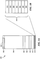
- FIG. 3A is a cross section of substrate 200 showing multiple layers of material.
- Substrate 200 includes a first layer 302 of dielectric material in which antenna elements 202 (and/or 204) may reside.
- first layer 302 may form the top surface of antenna component 12 and antenna array 10.
- Antenna elements 202 and 204 may be embedded or inlaid within first layer 302 so that the surface of antenna elements 202 and 204 is flush with the outer surface of first layer 302.
- antenna elements 202 and 204 may have a thickness greater or smaller than that of first layer 302. If the antenna elements have a smaller thickness, the antenna elements may not extend all the way through first layer 302, and if the antenna elements have a greater thickness, the antenna elements may extend through the first layer 302 into the second layer 304.
- first layer 302 and second layer 304 comprise a dielectric epoxy material.
- the material may have a dielectric constant of about 2.9 and a loss tangent of about 0.04.
- layer 304 may be formed on substrate 200.
- antenna elements 202 and 204 may be masked and/or etched or (or otherwise formed) onto the surface of layer 304.
- layer 302 of dielectric material may be deposited on top of layer 304 in the areas not covered by antenna elements 202 and 204.
- the dielectric material of layer 302 may be deposited onto the surface of substrate 200 so that layer 302 covers both layer 304 and the antenna elements.
- material may then be removed from the top surface of substrate 200 until antenna elements 202 and 204 are exposed and the surface of antenna element 202 and antenna element 204 is flush or parallel with the surface of layer 302.
- removal of the material to expose antenna elements 202 and 204 is not a requirement.
- Layers 302, 304, 308, and 312 may comprise the same or a similar dielectric epoxy.
- the dielectric epoxy in layers 302, 304, 308, and 312 may have a dielectric constant of about 2.9 and a loss tangent of about 0.04. These constants are provided as examples only; the material in layers 302, 304, 308, and 312 may have other dielectric constants and loss tangents as desired. Also, layers 302, 304, 308, and 312 may be formed from different dielectric materials if desired.
- Layers 306 and 308 are conductive layers.
- layers 306 and 308 may be copper, aluminum, gold, or any other type of conductive material.
- layers 306 and 308 are electrically connected to a ground reference and act as ground planes for the antenna array 10.
- Reference designator 314 denotes a multi-layered section of substrate 200. These layers in section 314 may be relatively thinner than layers 302, 304, 306, 308, 310, and/or 312. Accordingly, these layers 314 are broken out and enlarged in FIG. 3B .
- substrate 200 includes layers 316, 318, 320, 322, 324, 326, and/or 328.
- Layer 316 in an embodiment, may be a dielectric material such as a polyimide, and may have a dielectric constant of 6.5 and a loss tangent of 0.01.
- Layers 318-328 may also be dielectric materials such as silicon dioxide, doped silicon dioxide, other silicon dioxide composites, glass, glassy carbon, or other materials having desired dielectric properties.
- the layers of substrate 200 have properties according to the following table: Layer (Reference Designator) Material Dielectric Constant Loss Tangent Thickness (in ⁇ 0 ) 302 Dielectric Epoxy 2.9 0.04 0.002 304 Dielectric Epoxy 2.9 0.04 0.028 306 Copper (Conductor) 0.003 308 Dielectric Epoxy 2.9 0.04 0.006 310 Copper (Conductor) 0.003 312 Dielectric Epoxy 2.9 0.04 0.004 316 Dielectric Polyimide 6.5 0.01 0.0001 318 Dielectric 4.2 0.01 0.0002 320 Dielectric 6.5 0.01 0.0002 322 Dielectric 4.4 0.01 0.0002 324 Dielectric 3.9 0.03 0.001 326 Dielectric 4.2 0.01 0.0003 328 Dielectric 3.9 0.01 0.0001
- the table above illustrates an exemplary embodiment of the layers in substrate 200, and is not intended to limit the scope of the disclosure.
- the layers above can be removed, replaced, or modified with material having different properties as required by design requirements.
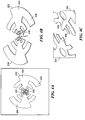
- FIGS. 4A, 4B, and 4C are illustrations of antenna elements 202 and 204.
- Antenna elements 202 and 204 may be a type of log-periodic toothed planar antenna.
- each antenna component 12 within antenna array 10 may include one more antenna elements 202 and/or 204.
- antenna elements 202 and 204 may comprise a conductive material such as copper.
- Antenna elements 202 and 204 may be substantially flat, i.e. planar, and may be inlaid or embedded in first layer 302 of dielectric material.
- Antenna elements 202 and 204 may comprise a log-periodic toothed planar array antenna, where antenna element 202 is one side of the log periodic planar antenna and antenna element 204 is the other side of the log periodic planar antenna.
- antenna element 202 has a central body 404 with a roughly triangular shape, with a point or apex of the triangle terminating at or near a central point 402. Extending from the central body 404 are a series of teeth or leaves 406. The leaves 406 extend from the body 404 and have a curvature or radius relative to central point 402.
- the leaves 406 closest to central point 402 may be relatively smaller in width and length, and the leaves 406 further from central point 402 may increase in width and length the further they are from central point 402. As shown, the leaves 406 extend from the body 404 in an alternating pattern relative to their distance from central point 402. In other words, as body 404 extends radially from central point 402, leaves 406 extend first from one side of body 404 then on the other side, etc., so that the leaves 406 alternate sides.
- the leaves 406 of the antenna may approximate the shape of a spiral planar antenna.
- leaves 406 need not form a spiral.
- the curvature of leaves 406 may follow a spiral pattern.
- leaves 406 may have a circular, elliptical, semi-circular, or arced pattern, as shown in FIGS 4A-4C .
- antenna elements 202 and 204 may each have four leaves 406 on one side of body 404 and five leaves on the other side of body 404. However, this is not a requirement. Antenna elements 202 and 204 can have more or fewer leaves 406 on each side of body 404. The leaves 406 may increase in length and thickness as they increase in distance from central point 402.
- Antenna element 202 may also include a hole 408. As shown in FIGS. 4A, 4B, and 4C , hole 408 is positioned relatively close to the center point 402. Hole 408 may have a diameter sufficiently large to allow a portion of a balun structure to extend through hole 408 and sufficiently small so that the inner surface of hole 408 makes electrical contact with the balun.
- Antenna elements 202 and 204 may be radially symmetric, i.e. antenna element 202 and antenna element 204 may be identical about the central point 402. Accordingly, antenna element 204 may include at least all the features described above with respect to antenna element 204 including, but not limited to, body 404, leaves 406, and hole 408.
- FIGS. 5A, 5B illustrate a cross section of a balun 502 included in antenna component 12.
- FIG. 5A shows balun 502 embedded within the substrate of antenna component 12
- FIG. 5B shows balun 502 apart from the substrate of antenna component 12
- FIG. 5C shows an isometric view of balun 502.
- Balun 502 may comprise a conductive material such as copper.
- balun 502 is formed from the same material as antenna elements 202 and/or 204. However, this is not a requirement.
- Balun 502 extends through substrate 200 substantially perpendicularly to antenna elements 202 and 204. By extending balun 500 down through the substrate, antenna component 12 can be constructed in a sub-compact arrangement because the area and volume used by antenna elements 202 and 104, and balun 502, is reduced.
- Balun 502 when electrically connected to antenna element 202 and antenna element 204, may act to extend the electrical length of antenna element 202 and antenna element 204 so that the antenna length is a multiple of a quarter wavelength of the intended frequency to be received by antenna component 12, i.e. so that the electrical length is the same as or similar to ⁇ 0 /4, ⁇ 0 /2, ⁇ 0 , etc.
- the electrical length of the antenna may be a quarter wavelength at a high frequency, but may be less than a quarter wavelength for slower frequencies, which can also be received by the antenna. This is due, at least in part, to the balun 502 being embedded in the layers of dielectric material, which effectively increases the electrical length of the balun 502.
- Balun 502 acts to electrically extend the length of the antenna by affecting the impedance, capacitance, resistance, and other electrical properties of the antenna.
- balun 502 may be embedded within dielectric layers of substrate 200.
- dielectric material may fill voids within balun 502, as shown in FIG. 5C .
- the geometry of balun 502 through the substrate material may allow balun 502 to affect the impedance and capacitance of the antenna to effectively extend the electrical length of the antenna.
- the electrical length of the antenna and/or the balun may be less than a quarter-wavelength of the intended frequency. As is known, extending the electrical length of the antenna can aid in reception of the intended frequencies by the antenna. In an embodiment, the electrical length of the antenna and/or the balun may be less than a quarter wavelength of the intended frequency.
- the dielectric material in which balun 502 is embedded, and which fills voids within balun 502 imparts electrical properties on balun 502 making balun appear (i.e. act) as though it is electrically longer than its physical dimensions.
- balun 502 may extend through multiple layers of substrate 200.
- balun 502 is embedded within the dielectric epoxy material of layers 302, 304, 308 and 312 (See FIG. 3A ).
- balun 502 may also be embedded in or extend through layers 316-328 (See FIG. 3B ).
- Balun 502 may also pass through conductive layers 306 and 308.
- conductive layers 306 and 308 may contain one or more holes through which balun 502 can extend so that balun 502 does not make direct electrical contact with layers 306 and 308, which may be coupled to ground.
- a conductive layer 306 (or a similar layer) is shown from a top view.
- Conductive layer 306 (and/or conductive layer 310) includes one or more holes 602 through which balun 502 can extend so that balun 502 does not come in direction contact with conductive layer 306 (and/or conductive layer 310).
- balun 502 comprises a series of annular sections 504.
- Annular sections 504 may be substantially cylindrical conductive elements having a hollow core 506, as seen in FIG. 5C .
- the hollow core 506 may be filled with a dielectric material, which may be the same as or similar to the dielectric epoxy comprising the layers of substrate 200.
- the annular sections may all have the same diameter, or may have differing diameters as desired.
- Annular sections 504 may each have a top end 507 and a bottom end 508 coupled to a substantially planar conductive element 510. Annular sections 504 and conductive elements 510 are connected to form a transverse pattern where annular sections 504 are placed in alternating positions with respect to conductive elements 510. This so-called alternating staircase pattern forms a substantially alternating or zigzag conduction path as shown by line 512. This allows balun 512 to provide a sufficiently long conduction path for antenna component 12 to receive microwave signals while conserving the amount of area and/or volume used by balun 512 within substrate 200.
- balun 502 may include more or fewer than three annular sections (and thus more or fewer conductive elements 510) as desired. Reducing the number of annular sections 504 may reduce the electrical length of balun 502 and increasing the number of annular sections 504 may increase the electrical length of balun 502.
- Balun 502 also includes one or more antenna connectors 514 that electrically couple balun 502 to antenna elements 202 and 204.
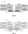
- Antenna connectors 514 may extend through the holes 408 in the antenna elements 202 and 204, as shown in FIG. 7A and 7B . Accordingly, antenna connectors 514 may have a diameter sufficiently large so that the outer surface of connectors 514 comes in electrical contact with the inner surface of holes 408.
- Antenna connectors 514 may be annular connectors with a substantially cylindrical shape, and may have a hollow core 506.
- the hollow core 506 may be filled with a dielectric material similar to or the same as the dielectric material used in one or more of the layers of substrate 200.
- the diameter of the connectors 514 and holes 408 may be smaller than the diameter of annular sections 504. However, this is not a requirement. In other embodiments, the diameter of connectors 514 and holes 408 may be the same as or greater than the diameters of annular sections 504.
- balun 502 may also comprise one or more terminal connectors 516.
- Terminal connectors 516 may also be substantially cylindrical annular sections having a hollow core (not shown) filled with dielectric material.
- the dielectric material may be similar to or the same as the dielectric material comprising one or more layers of substrate 200.
- terminal connectors 516 are coupled to external circuitry capable of receiving signals from antenna component 12.
- terminal connectors 516 may be coupled to an amplifier, a filter, a processor, or another circuit capable of receiving and processing signals coupled by antenna component 12 as antenna component 12 receives microwave transmissions and signals.
- terminal connectors 516 extend through the bottom substrate 200 so that external, electrical connections can be made to terminal connectors 516.
- terminal connectors 516 are embedded within substrate 200 and are coupled to connectors that extend externally to substrate 200.
- terminal connectors 516 are coupled to connection pads 802.
- Connection pads 802 may be placed on or proximate to the bottom of substrate 200 so that they come in contact with the portion of terminal connectors 516 that extend through substrate 200.
- connection pads 802 may be embedded within the material of substrate 200.
- Connection pads 802 may be made from a conductor, such as copper or gold, to facilitate electrical connection between balun 512 and external circuitry.
- Connection pads 802 may be coupled to a signal lead, such as signal lead 902 in FIG. 9 .
- Signal lead 902 can extend externally to substrate 200 and can be connected to external circuitry that receives and processes the signal received by the antenna.
- signal lead 902 is coupled to an external low noise amplifier (LNA) and/or filter that receives the signal from antenna component 12.
- LNA low noise amplifier
- a signal lead may be coupled to and extend from each connection pad 802.
- a conductor 904 may be positioned adjacent to the signal leads 902.
- conductor 902 may be positioned below signal leads 902.
- Conductor 904 may be coupled to a ground reference so that conductor 904 acts as a ground plane to enhance signal quality of the signals on signal leads 902. Additionally/alternatively, conductor 904 may act as an impedance transformer to match the impedance of the signal paths of the antenna to external circuitry connections.
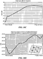
- FIG. 10A, 10B , 10C, and 10D are graphs showing performance of an exemplary embodiment of the antenna described above.
- FIG. 10A is a 3D plot showing field of view and realized gain at a frequency ⁇ 0 .
- FIG. 10B is a 2D field of view and realized gain from including frequencies in the W band and the V band.
- FIG. 10C is a graph of the peak gain of a signal received by the antenna v. frequency.
- the vertical axis represents gain and the horizontal axis represents the frequency.
- the frequency on the horizontal axis ranges from a low in-band frequency to a high in-band frequency.
- FIG. 10D is a graph showing isolation performance between four adjacently placed antenna components 12.
- the vertical axis represents decibels (where the top of the vertical axis is -30dB) and the horizontal axis represents frequencies ranging from a low in-band frequency to a high in-band frequency.
- an antenna component 12 may be used to receive microwave transmissions or signals.
- Antenna component 12 may be used as a single (i.e. stand-alone) element, or may be incorporated into an antenna array 10.
- antenna array 10 may receive multiple microwave transmissions.
- each antenna component 12 within antenna array 10 may receive a separate microwave transmission.
- each antenna component 12 represents photonic detector and the signal produced by each antenna component 12 represents a pixel that can be subsequently processed and reconstructed to form a two dimensional image of the original signal source.
- the original signal source is a body that generates random heat, i.e. a randomly generated heat source.
- Antenna component 12 and antenna array 10 may be useful in various application including imaging, missile guidance, targeting, surveillance, etc.
Landscapes
- Details Of Aerials (AREA)
- Physics & Mathematics (AREA)
- Engineering & Computer Science (AREA)
- Variable-Direction Aerials And Aerial Arrays (AREA)
- Electromagnetism (AREA)
- Computer Networks & Wireless Communication (AREA)
- General Physics & Mathematics (AREA)
- Radar, Positioning & Navigation (AREA)
- Remote Sensing (AREA)
Claims (11)
- Appareil ultracompact faisant antenne (12) comprenant :une pluralité de couches de matériau diélectrique ;une antenne encastrée dans une couche supérieure du matériau diélectrique (302) de telle sorte qu'une surface de l'antenne est sensiblement parallèle à une surface extérieure de la couche supérieure de matériau diélectrique (302) ; etun symétriseur conducteur en escalier (502), couplé à l'antenne, et incorporé dans une ou plusieurs couches du matériau diélectrique, le symétriseur conducteur en escalier (502) comprenant des segments sensiblement plans et des segments sensiblement annulaires (504) ;dans lequel les segments plans et les segments annulaires (504) sont disposés en un motif transversal où des sections annulaires sont placées dans des positions alternées par rapport aux segments plans pour former un chemin de conduction alterné ou en zigzag ;dans lequel le symétriseur (502) est incorporé dans et s'étend à travers au moins une partie de la pluralité de couches dans une direction sensiblement perpendiculaire à l'antenne ; etdans lequel des cavités (506) des segments annulaires (504) sont remplies avec un matériau diélectrique.
- Appareil de la revendication 1 comprenant en outre au moins une couche conductrice (306, 310) entre les couches de matériau diélectrique.
- Appareil de la revendication 2 dans lequel l'au moins une couche conductrice (306, 310) contient un trou (602) à travers lequel s'étend le symétriseur (502).
- Appareil de la revendication 2 dans lequel l'au moins une couche conductrice (306, 310) est une couche de masse.
- Appareil de la revendication 1 dans lequel la pluralité de couches de matériau diélectrique comporte onze couches de matériau diélectrique, une couche conductrice (306) entre les deuxième et troisième couches de matériau diélectrique, et une couche conductrice (310) entre les troisième et quatrième couches de matériau diélectrique.
- Appareil de la revendication 1 dans lequel l'antenne est une antenne plane.
- Appareil de la revendication 1 dans lequel l'antenne est une antenne dentée log-périodique.
- Appareil de la revendication 1 dans lequel l'antenne comporte un trou (408), et le symétriseur (502) comprend une section cylindrique (514) adaptée pour s'étendre à travers le trou pour coupler l'antenne au symétriseur.
- Appareil de la revendication 1 comprenant en outre un transformateur d'impédance couplé au symétriseur (502).
- Appareil de la revendication 1 dans lequel l'antenne est une antenne plane dentée log-périodique comprenant deux sections conductrices sensiblement planes (202, 204), les sections conductrices sensiblement planes étant encastrées dans une couche supérieure du matériau diélectrique (302) de telle sorte qu'une surface supérieure des sections conductrices sensiblement planes (202, 204) est sensiblement parallèle à une surface extérieure de la couche supérieure de matériau diélectrique (302).
- Système d'imagerie (10) comprenant :
un réseau bidimensionnel de sections d'antenne (12), chaque section d'antenne (12) comprenant l'appareil de l'une quelconque des revendications 1 à 10.
Applications Claiming Priority (2)
| Application Number | Priority Date | Filing Date | Title |
|---|---|---|---|
| US13/925,109 US9329255B2 (en) | 2013-06-24 | 2013-06-24 | Imaging antenna and related techniques |
| PCT/US2014/042698 WO2014209678A1 (fr) | 2013-06-24 | 2014-06-17 | Imagerie d'antenne logarithme périodique comportant un symétriseur en escalier et techniques associées |
Publications (2)
| Publication Number | Publication Date |
|---|---|
| EP3014697A1 EP3014697A1 (fr) | 2016-05-04 |
| EP3014697B1 true EP3014697B1 (fr) | 2021-04-14 |
Family
ID=51134447
Family Applications (1)
| Application Number | Title | Priority Date | Filing Date |
|---|---|---|---|
| EP14736251.1A Active EP3014697B1 (fr) | 2013-06-24 | 2014-06-17 | Imagerie d'antenne logarithme périodique comportant un symétriseur en escalier et techniques associées |
Country Status (6)
| Country | Link |
|---|---|
| US (1) | US9329255B2 (fr) |
| EP (1) | EP3014697B1 (fr) |
| JP (1) | JP6193488B2 (fr) |
| IL (1) | IL241972B (fr) |
| TW (1) | TWI587576B (fr) |
| WO (1) | WO2014209678A1 (fr) |
Families Citing this family (12)
| Publication number | Priority date | Publication date | Assignee | Title |
|---|---|---|---|---|
| US9980300B2 (en) * | 2016-04-29 | 2018-05-22 | The Boeing Company | Wearables making a link to communication systems |
| CN107017469B (zh) * | 2017-04-12 | 2020-05-22 | 电子科技大学 | 一种低剖面全向扫描端射天线阵列 |
| CN107359418B (zh) * | 2017-05-31 | 2019-11-29 | 上海华为技术有限公司 | 一种多频天线系统及控制多频天线系统内异频干扰的方法 |
| CN107464995A (zh) * | 2017-08-01 | 2017-12-12 | 全普光电科技(上海)有限公司 | 一种薄膜天线及其制备方法 |
| WO2019133703A2 (fr) * | 2017-12-29 | 2019-07-04 | Massachusetts Institute Of Technology | Systèmes de radiomètres et procédés |
| US10983245B2 (en) | 2017-12-29 | 2021-04-20 | Massachusetts Institute Of Technology | Radiometer systems and methods |
| CN111313155B (zh) | 2018-12-11 | 2021-11-19 | 华为技术有限公司 | 天线和通信设备 |
| CN112448157B (zh) * | 2020-11-10 | 2022-04-22 | 安徽大学 | 基于多层pcb的毫米波集成对数周期天线 |
| CN112909539B (zh) * | 2021-01-20 | 2022-02-22 | 西安交通大学 | 一种毫米波频率极化双随机多端口聚束天线 |
| US11876278B2 (en) * | 2021-03-29 | 2024-01-16 | Raytheon Company | Balun comprising stepped transitions between balance and unbalance connections, where the stepped transitions include ground rings of differing lengths connected by caged vias |
| WO2025206801A1 (fr) * | 2024-03-29 | 2025-10-02 | 주식회사 에이피알 | Dispositif d'antenne |
| CN119764844B (zh) * | 2024-12-17 | 2025-10-03 | 安徽大学 | 一种自互补对数周期齿形介质谐振器天线 |
Family Cites Families (24)
| Publication number | Priority date | Publication date | Assignee | Title |
|---|---|---|---|---|
| US3681771A (en) * | 1970-03-23 | 1972-08-01 | Macdowell Associates Inc | Retroflector dipole antenna array and method of making |
| US4746925A (en) * | 1985-07-31 | 1988-05-24 | Toyota Jidosha Kabushiki Kaisha | Shielded dipole glass antenna with coaxial feed |
| US5046707A (en) | 1988-11-30 | 1991-09-10 | The United States Of America As Represented By The Secretary Of The Air Force | Spherical positioning pin |
| US5212494A (en) * | 1989-04-18 | 1993-05-18 | Texas Instruments Incorporated | Compact multi-polarized broadband antenna |
| US5313216A (en) | 1991-05-03 | 1994-05-17 | Georgia Tech Research Corporation | Multioctave microstrip antenna |
| JP3083416B2 (ja) | 1992-11-06 | 2000-09-04 | 進工業株式会社 | ディレイライン素子およびその製造方法 |
| JP3123363B2 (ja) | 1994-10-04 | 2001-01-09 | 三菱電機株式会社 | 携帯無線機 |
| JPH0974307A (ja) | 1995-09-05 | 1997-03-18 | Murata Mfg Co Ltd | チップアンテナ |
| JPH10163710A (ja) * | 1996-11-27 | 1998-06-19 | Kyocera Corp | 高周波用伝送線路 |
| US6046707A (en) | 1997-07-02 | 2000-04-04 | Kyocera America, Inc. | Ceramic multilayer helical antenna for portable radio or microwave communication apparatus |
| JP2001102696A (ja) * | 1999-09-30 | 2001-04-13 | Kyocera Corp | 配線基板及びその製造方法 |
| US6819199B2 (en) * | 2001-01-22 | 2004-11-16 | Broadcom Corporation | Balun transformer with means for reducing a physical dimension thereof |
| US8547186B2 (en) * | 2005-09-09 | 2013-10-01 | Anaren, Inc. | Compact balun |
| US7176776B1 (en) * | 2006-05-04 | 2007-02-13 | Delphi Technologies, Inc. | Multi-layer RF filter and balun |
| JP2008028836A (ja) * | 2006-07-24 | 2008-02-07 | Fujitsu Ltd | 超伝導フィルタデバイスおよびその作製方法 |
| JP4500840B2 (ja) | 2006-12-08 | 2010-07-14 | 太陽誘電株式会社 | 積層型バラン及び混成集積回路モジュール並びに積層基板 |
| US7528676B2 (en) * | 2007-04-16 | 2009-05-05 | Tdk Corporation | Balun circuit suitable for integration with chip antenna |
| US7675466B2 (en) * | 2007-07-02 | 2010-03-09 | International Business Machines Corporation | Antenna array feed line structures for millimeter wave applications |
| US8264410B1 (en) * | 2007-07-31 | 2012-09-11 | Wang Electro-Opto Corporation | Planar broadband traveling-wave beam-scan array antennas |
| US20090179716A1 (en) | 2008-01-09 | 2009-07-16 | Anaren, Inc. | RF Filter Device |
| US7859359B2 (en) * | 2008-02-25 | 2010-12-28 | Broadcom Corporation | Method and system for a balun embedded in an integrated circuit package |
| US8265410B1 (en) | 2009-07-11 | 2012-09-11 | Luxand, Inc. | Automatic correction and enhancement of facial images |
| US8390529B1 (en) | 2010-06-24 | 2013-03-05 | Rockwell Collins, Inc. | PCB spiral antenna and feed network for ELINT applications |
| WO2012085670A1 (fr) * | 2010-12-23 | 2012-06-28 | Marvell World Trade Ltd. | Transformateur symétrique-dissymétrique en forme de chiffre huit |
-
2013
- 2013-06-24 US US13/925,109 patent/US9329255B2/en active Active
-
2014
- 2014-06-17 WO PCT/US2014/042698 patent/WO2014209678A1/fr not_active Ceased
- 2014-06-17 EP EP14736251.1A patent/EP3014697B1/fr active Active
- 2014-06-17 JP JP2016523790A patent/JP6193488B2/ja active Active
- 2014-06-20 TW TW103121367A patent/TWI587576B/zh active
-
2015
- 2015-10-08 IL IL241972A patent/IL241972B/en active IP Right Grant
Non-Patent Citations (1)
| Title |
|---|
| None * |
Also Published As
| Publication number | Publication date |
|---|---|
| US9329255B2 (en) | 2016-05-03 |
| WO2014209678A1 (fr) | 2014-12-31 |
| TW201513462A (zh) | 2015-04-01 |
| JP6193488B2 (ja) | 2017-09-06 |
| US20140374616A1 (en) | 2014-12-25 |
| IL241972B (en) | 2019-07-31 |
| EP3014697A1 (fr) | 2016-05-04 |
| JP2016529771A (ja) | 2016-09-23 |
| TWI587576B (zh) | 2017-06-11 |
Similar Documents
| Publication | Publication Date | Title |
|---|---|---|
| EP3014697B1 (fr) | Imagerie d'antenne logarithme périodique comportant un symétriseur en escalier et techniques associées | |
| EP3275045B1 (fr) | Appareil et procédé pour un élément d'antenne à large bande et grande efficacité d'ouverture avec gain stable | |
| TWI420739B (zh) | 輻射場型隔離器及其天線系統與使用該天線系統的通訊裝置 | |
| US9425516B2 (en) | Compact dual band GNSS antenna design | |
| JP6258045B2 (ja) | アンテナ | |
| US20060001574A1 (en) | Wideband Patch Antenna | |
| KR20090013228A (ko) | 안테나 시스템 | |
| CN102460832A (zh) | 用于无线电波的发射和接收的小型超宽带天线 | |
| KR102218801B1 (ko) | 어레이 안테나 장치 | |
| CN102460830A (zh) | 用于移动手持电话和计算机网络的电小超宽带天线 | |
| CN105428804B (zh) | 一种采用圆柱共形电磁带隙结构的宽波束圆极化y形-h形槽小型化圆贴片天线 | |
| WO2019111025A1 (fr) | Antenne | |
| US6906683B2 (en) | Circular polarized wave reception antenna | |
| WO2018159668A1 (fr) | Dispositif antenne | |
| CN116613547A (zh) | 一种具有高孔径复用率和高端口隔离的双频共孔径天线 | |
| KR101070287B1 (ko) | 핀 배열 패치 안테나의 설계 방법, 그 핀 배열 패치 안테나를 이용한 위상 배열 안테나의 설계 방법 및 그 기록 매체 | |
| US7990322B1 (en) | Shortened HF and VHF antennas made with concentric ceramic cylinders | |
| Hasan et al. | Dual band slotted printed circular patch antenna with superstrate and EBG structure for 5G applications | |
| JP2007336296A (ja) | 平面型アンテナ | |
| US12362450B2 (en) | Additively manufactured cluster connector | |
| US7414591B1 (en) | Helical antenna system | |
| JP2013187731A (ja) | アンテナ装置 | |
| JP6590936B2 (ja) | 広帯域幅および円偏波のための同軸ホーン励起法 | |
| US20210384628A1 (en) | Ultra wideband antenna structure | |
| WO2018118996A1 (fr) | Antenne en spirale à ondes millimétriques avec symétriseur distribué |
Legal Events
| Date | Code | Title | Description |
|---|---|---|---|
| PUAI | Public reference made under article 153(3) epc to a published international application that has entered the european phase |
Free format text: ORIGINAL CODE: 0009012 |
|
| 17P | Request for examination filed |
Effective date: 20160114 |
|
| AK | Designated contracting states |
Kind code of ref document: A1 Designated state(s): AL AT BE BG CH CY CZ DE DK EE ES FI FR GB GR HR HU IE IS IT LI LT LU LV MC MK MT NL NO PL PT RO RS SE SI SK SM TR |
|
| AX | Request for extension of the european patent |
Extension state: BA ME |
|
| DAX | Request for extension of the european patent (deleted) | ||
| STAA | Information on the status of an ep patent application or granted ep patent |
Free format text: STATUS: EXAMINATION IS IN PROGRESS |
|
| 17Q | First examination report despatched |
Effective date: 20190103 |
|
| GRAP | Despatch of communication of intention to grant a patent |
Free format text: ORIGINAL CODE: EPIDOSNIGR1 |
|
| STAA | Information on the status of an ep patent application or granted ep patent |
Free format text: STATUS: GRANT OF PATENT IS INTENDED |
|
| INTG | Intention to grant announced |
Effective date: 20201109 |
|
| GRAS | Grant fee paid |
Free format text: ORIGINAL CODE: EPIDOSNIGR3 |
|
| GRAA | (expected) grant |
Free format text: ORIGINAL CODE: 0009210 |
|
| STAA | Information on the status of an ep patent application or granted ep patent |
Free format text: STATUS: THE PATENT HAS BEEN GRANTED |
|
| AK | Designated contracting states |
Kind code of ref document: B1 Designated state(s): AL AT BE BG CH CY CZ DE DK EE ES FI FR GB GR HR HU IE IS IT LI LT LU LV MC MK MT NL NO PL PT RO RS SE SI SK SM TR |
|
| REG | Reference to a national code |
Ref country code: GB Ref legal event code: FG4D |
|
| REG | Reference to a national code |
Ref country code: CH Ref legal event code: EP |
|
| REG | Reference to a national code |
Ref country code: DE Ref legal event code: R096 Ref document number: 602014076569 Country of ref document: DE |
|
| REG | Reference to a national code |
Ref country code: IE Ref legal event code: FG4D |
|
| REG | Reference to a national code |
Ref country code: AT Ref legal event code: REF Ref document number: 1383276 Country of ref document: AT Kind code of ref document: T Effective date: 20210515 |
|
| REG | Reference to a national code |
Ref country code: LT Ref legal event code: MG9D |
|
| REG | Reference to a national code |
Ref country code: AT Ref legal event code: MK05 Ref document number: 1383276 Country of ref document: AT Kind code of ref document: T Effective date: 20210414 |
|
| REG | Reference to a national code |
Ref country code: NL Ref legal event code: MP Effective date: 20210414 |
|
| PG25 | Lapsed in a contracting state [announced via postgrant information from national office to epo] |
Ref country code: AT Free format text: LAPSE BECAUSE OF FAILURE TO SUBMIT A TRANSLATION OF THE DESCRIPTION OR TO PAY THE FEE WITHIN THE PRESCRIBED TIME-LIMIT Effective date: 20210414 Ref country code: BG Free format text: LAPSE BECAUSE OF FAILURE TO SUBMIT A TRANSLATION OF THE DESCRIPTION OR TO PAY THE FEE WITHIN THE PRESCRIBED TIME-LIMIT Effective date: 20210714 Ref country code: FI Free format text: LAPSE BECAUSE OF FAILURE TO SUBMIT A TRANSLATION OF THE DESCRIPTION OR TO PAY THE FEE WITHIN THE PRESCRIBED TIME-LIMIT Effective date: 20210414 Ref country code: LT Free format text: LAPSE BECAUSE OF FAILURE TO SUBMIT A TRANSLATION OF THE DESCRIPTION OR TO PAY THE FEE WITHIN THE PRESCRIBED TIME-LIMIT Effective date: 20210414 Ref country code: NL Free format text: LAPSE BECAUSE OF FAILURE TO SUBMIT A TRANSLATION OF THE DESCRIPTION OR TO PAY THE FEE WITHIN THE PRESCRIBED TIME-LIMIT Effective date: 20210414 Ref country code: HR Free format text: LAPSE BECAUSE OF FAILURE TO SUBMIT A TRANSLATION OF THE DESCRIPTION OR TO PAY THE FEE WITHIN THE PRESCRIBED TIME-LIMIT Effective date: 20210414 |
|
| PG25 | Lapsed in a contracting state [announced via postgrant information from national office to epo] |
Ref country code: LV Free format text: LAPSE BECAUSE OF FAILURE TO SUBMIT A TRANSLATION OF THE DESCRIPTION OR TO PAY THE FEE WITHIN THE PRESCRIBED TIME-LIMIT Effective date: 20210414 Ref country code: IS Free format text: LAPSE BECAUSE OF FAILURE TO SUBMIT A TRANSLATION OF THE DESCRIPTION OR TO PAY THE FEE WITHIN THE PRESCRIBED TIME-LIMIT Effective date: 20210814 Ref country code: GR Free format text: LAPSE BECAUSE OF FAILURE TO SUBMIT A TRANSLATION OF THE DESCRIPTION OR TO PAY THE FEE WITHIN THE PRESCRIBED TIME-LIMIT Effective date: 20210715 Ref country code: NO Free format text: LAPSE BECAUSE OF FAILURE TO SUBMIT A TRANSLATION OF THE DESCRIPTION OR TO PAY THE FEE WITHIN THE PRESCRIBED TIME-LIMIT Effective date: 20210714 Ref country code: PL Free format text: LAPSE BECAUSE OF FAILURE TO SUBMIT A TRANSLATION OF THE DESCRIPTION OR TO PAY THE FEE WITHIN THE PRESCRIBED TIME-LIMIT Effective date: 20210414 Ref country code: PT Free format text: LAPSE BECAUSE OF FAILURE TO SUBMIT A TRANSLATION OF THE DESCRIPTION OR TO PAY THE FEE WITHIN THE PRESCRIBED TIME-LIMIT Effective date: 20210816 Ref country code: ES Free format text: LAPSE BECAUSE OF FAILURE TO SUBMIT A TRANSLATION OF THE DESCRIPTION OR TO PAY THE FEE WITHIN THE PRESCRIBED TIME-LIMIT Effective date: 20210414 Ref country code: RS Free format text: LAPSE BECAUSE OF FAILURE TO SUBMIT A TRANSLATION OF THE DESCRIPTION OR TO PAY THE FEE WITHIN THE PRESCRIBED TIME-LIMIT Effective date: 20210414 Ref country code: SE Free format text: LAPSE BECAUSE OF FAILURE TO SUBMIT A TRANSLATION OF THE DESCRIPTION OR TO PAY THE FEE WITHIN THE PRESCRIBED TIME-LIMIT Effective date: 20210414 |
|
| REG | Reference to a national code |
Ref country code: DE Ref legal event code: R097 Ref document number: 602014076569 Country of ref document: DE |
|
| PG25 | Lapsed in a contracting state [announced via postgrant information from national office to epo] |
Ref country code: EE Free format text: LAPSE BECAUSE OF FAILURE TO SUBMIT A TRANSLATION OF THE DESCRIPTION OR TO PAY THE FEE WITHIN THE PRESCRIBED TIME-LIMIT Effective date: 20210414 Ref country code: CZ Free format text: LAPSE BECAUSE OF FAILURE TO SUBMIT A TRANSLATION OF THE DESCRIPTION OR TO PAY THE FEE WITHIN THE PRESCRIBED TIME-LIMIT Effective date: 20210414 Ref country code: DK Free format text: LAPSE BECAUSE OF FAILURE TO SUBMIT A TRANSLATION OF THE DESCRIPTION OR TO PAY THE FEE WITHIN THE PRESCRIBED TIME-LIMIT Effective date: 20210414 Ref country code: SK Free format text: LAPSE BECAUSE OF FAILURE TO SUBMIT A TRANSLATION OF THE DESCRIPTION OR TO PAY THE FEE WITHIN THE PRESCRIBED TIME-LIMIT Effective date: 20210414 Ref country code: SM Free format text: LAPSE BECAUSE OF FAILURE TO SUBMIT A TRANSLATION OF THE DESCRIPTION OR TO PAY THE FEE WITHIN THE PRESCRIBED TIME-LIMIT Effective date: 20210414 Ref country code: RO Free format text: LAPSE BECAUSE OF FAILURE TO SUBMIT A TRANSLATION OF THE DESCRIPTION OR TO PAY THE FEE WITHIN THE PRESCRIBED TIME-LIMIT Effective date: 20210414 Ref country code: MC Free format text: LAPSE BECAUSE OF FAILURE TO SUBMIT A TRANSLATION OF THE DESCRIPTION OR TO PAY THE FEE WITHIN THE PRESCRIBED TIME-LIMIT Effective date: 20210414 |
|
| REG | Reference to a national code |
Ref country code: CH Ref legal event code: PL |
|
| PLBE | No opposition filed within time limit |
Free format text: ORIGINAL CODE: 0009261 |
|
| STAA | Information on the status of an ep patent application or granted ep patent |
Free format text: STATUS: NO OPPOSITION FILED WITHIN TIME LIMIT |
|
| REG | Reference to a national code |
Ref country code: BE Ref legal event code: MM Effective date: 20210630 |
|
| 26N | No opposition filed |
Effective date: 20220117 |
|
| PG25 | Lapsed in a contracting state [announced via postgrant information from national office to epo] |
Ref country code: LU Free format text: LAPSE BECAUSE OF NON-PAYMENT OF DUE FEES Effective date: 20210617 |
|
| PG25 | Lapsed in a contracting state [announced via postgrant information from national office to epo] |
Ref country code: LI Free format text: LAPSE BECAUSE OF NON-PAYMENT OF DUE FEES Effective date: 20210630 Ref country code: IE Free format text: LAPSE BECAUSE OF NON-PAYMENT OF DUE FEES Effective date: 20210617 Ref country code: CH Free format text: LAPSE BECAUSE OF NON-PAYMENT OF DUE FEES Effective date: 20210630 |
|
| PG25 | Lapsed in a contracting state [announced via postgrant information from national office to epo] |
Ref country code: IS Free format text: LAPSE BECAUSE OF FAILURE TO SUBMIT A TRANSLATION OF THE DESCRIPTION OR TO PAY THE FEE WITHIN THE PRESCRIBED TIME-LIMIT Effective date: 20210814 Ref country code: AL Free format text: LAPSE BECAUSE OF FAILURE TO SUBMIT A TRANSLATION OF THE DESCRIPTION OR TO PAY THE FEE WITHIN THE PRESCRIBED TIME-LIMIT Effective date: 20210414 |
|
| PG25 | Lapsed in a contracting state [announced via postgrant information from national office to epo] |
Ref country code: IT Free format text: LAPSE BECAUSE OF FAILURE TO SUBMIT A TRANSLATION OF THE DESCRIPTION OR TO PAY THE FEE WITHIN THE PRESCRIBED TIME-LIMIT Effective date: 20210414 Ref country code: BE Free format text: LAPSE BECAUSE OF NON-PAYMENT OF DUE FEES Effective date: 20210630 |
|
| PG25 | Lapsed in a contracting state [announced via postgrant information from national office to epo] |
Ref country code: HU Free format text: LAPSE BECAUSE OF FAILURE TO SUBMIT A TRANSLATION OF THE DESCRIPTION OR TO PAY THE FEE WITHIN THE PRESCRIBED TIME-LIMIT; INVALID AB INITIO Effective date: 20140617 |
|
| PG25 | Lapsed in a contracting state [announced via postgrant information from national office to epo] |
Ref country code: CY Free format text: LAPSE BECAUSE OF FAILURE TO SUBMIT A TRANSLATION OF THE DESCRIPTION OR TO PAY THE FEE WITHIN THE PRESCRIBED TIME-LIMIT Effective date: 20210414 |
|
| P01 | Opt-out of the competence of the unified patent court (upc) registered |
Effective date: 20230530 |
|
| PG25 | Lapsed in a contracting state [announced via postgrant information from national office to epo] |
Ref country code: MK Free format text: LAPSE BECAUSE OF FAILURE TO SUBMIT A TRANSLATION OF THE DESCRIPTION OR TO PAY THE FEE WITHIN THE PRESCRIBED TIME-LIMIT Effective date: 20210414 |
|
| PG25 | Lapsed in a contracting state [announced via postgrant information from national office to epo] |
Ref country code: MT Free format text: LAPSE BECAUSE OF FAILURE TO SUBMIT A TRANSLATION OF THE DESCRIPTION OR TO PAY THE FEE WITHIN THE PRESCRIBED TIME-LIMIT Effective date: 20210414 |
|
| PGFP | Annual fee paid to national office [announced via postgrant information from national office to epo] |
Ref country code: DE Payment date: 20250520 Year of fee payment: 12 |
|
| PGFP | Annual fee paid to national office [announced via postgrant information from national office to epo] |
Ref country code: GB Payment date: 20250520 Year of fee payment: 12 |
|
| PGFP | Annual fee paid to national office [announced via postgrant information from national office to epo] |
Ref country code: FR Payment date: 20250520 Year of fee payment: 12 |
|
| PG25 | Lapsed in a contracting state [announced via postgrant information from national office to epo] |
Ref country code: TR Free format text: LAPSE BECAUSE OF FAILURE TO SUBMIT A TRANSLATION OF THE DESCRIPTION OR TO PAY THE FEE WITHIN THE PRESCRIBED TIME-LIMIT Effective date: 20210414 |