EP3014764B1 - Circuit d'amplificateur et methode correspondante - Google Patents
Circuit d'amplificateur et methode correspondante Download PDFInfo
- Publication number
- EP3014764B1 EP3014764B1 EP13740219.4A EP13740219A EP3014764B1 EP 3014764 B1 EP3014764 B1 EP 3014764B1 EP 13740219 A EP13740219 A EP 13740219A EP 3014764 B1 EP3014764 B1 EP 3014764B1
- Authority
- EP
- European Patent Office
- Prior art keywords
- amplifier
- stage
- quarter wavelength
- wavelength transmission
- amplifiers
- Prior art date
- Legal status (The legal status is an assumption and is not a legal conclusion. Google has not performed a legal analysis and makes no representation as to the accuracy of the status listed.)
- Active
Links
Images














Classifications
-
- H—ELECTRICITY
- H03—ELECTRONIC CIRCUITRY
- H03F—AMPLIFIERS
- H03F1/00—Details of amplifiers with only discharge tubes, only semiconductor devices or only unspecified devices as amplifying elements
- H03F1/02—Modifications of amplifiers to raise the efficiency, e.g. gliding Class A stages, use of an auxiliary oscillation
- H03F1/0205—Modifications of amplifiers to raise the efficiency, e.g. gliding Class A stages, use of an auxiliary oscillation in transistor amplifiers
- H03F1/0288—Modifications of amplifiers to raise the efficiency, e.g. gliding Class A stages, use of an auxiliary oscillation in transistor amplifiers using a main and one or several auxiliary peaking amplifiers whereby the load is connected to the main amplifier using an impedance inverter, e.g. Doherty amplifiers
-
- H—ELECTRICITY
- H01—ELECTRIC ELEMENTS
- H01P—WAVEGUIDES; RESONATORS, LINES, OR OTHER DEVICES OF THE WAVEGUIDE TYPE
- H01P5/00—Coupling devices of the waveguide type
- H01P5/12—Coupling devices having more than two ports
-
- H—ELECTRICITY
- H03—ELECTRONIC CIRCUITRY
- H03F—AMPLIFIERS
- H03F1/00—Details of amplifiers with only discharge tubes, only semiconductor devices or only unspecified devices as amplifying elements
- H03F1/02—Modifications of amplifiers to raise the efficiency, e.g. gliding Class A stages, use of an auxiliary oscillation
- H03F1/0205—Modifications of amplifiers to raise the efficiency, e.g. gliding Class A stages, use of an auxiliary oscillation in transistor amplifiers
- H03F1/0294—Modifications of amplifiers to raise the efficiency, e.g. gliding Class A stages, use of an auxiliary oscillation in transistor amplifiers using vector summing of two or more constant amplitude phase-modulated signals
-
- H—ELECTRICITY
- H03—ELECTRONIC CIRCUITRY
- H03F—AMPLIFIERS
- H03F3/00—Amplifiers with only discharge tubes or only semiconductor devices as amplifying elements
- H03F3/189—High-frequency amplifiers, e.g. radio frequency amplifiers
- H03F3/19—High-frequency amplifiers, e.g. radio frequency amplifiers with semiconductor devices only
-
- H—ELECTRICITY
- H03—ELECTRONIC CIRCUITRY
- H03F—AMPLIFIERS
- H03F3/00—Amplifiers with only discharge tubes or only semiconductor devices as amplifying elements
- H03F3/189—High-frequency amplifiers, e.g. radio frequency amplifiers
- H03F3/19—High-frequency amplifiers, e.g. radio frequency amplifiers with semiconductor devices only
- H03F3/195—High-frequency amplifiers, e.g. radio frequency amplifiers with semiconductor devices only in integrated circuits
-
- H—ELECTRICITY
- H03—ELECTRONIC CIRCUITRY
- H03F—AMPLIFIERS
- H03F3/00—Amplifiers with only discharge tubes or only semiconductor devices as amplifying elements
- H03F3/20—Power amplifiers, e.g. Class B amplifiers, Class C amplifiers
- H03F3/21—Power amplifiers, e.g. Class B amplifiers, Class C amplifiers with semiconductor devices only
- H03F3/211—Power amplifiers, e.g. Class B amplifiers, Class C amplifiers with semiconductor devices only using a combination of several amplifiers
-
- H—ELECTRICITY
- H03—ELECTRONIC CIRCUITRY
- H03F—AMPLIFIERS
- H03F3/00—Amplifiers with only discharge tubes or only semiconductor devices as amplifying elements
- H03F3/20—Power amplifiers, e.g. Class B amplifiers, Class C amplifiers
- H03F3/24—Power amplifiers, e.g. Class B amplifiers, Class C amplifiers of transmitter output stages
- H03F3/245—Power amplifiers, e.g. Class B amplifiers, Class C amplifiers of transmitter output stages with semiconductor devices only
-
- H—ELECTRICITY
- H03—ELECTRONIC CIRCUITRY
- H03F—AMPLIFIERS
- H03F3/00—Amplifiers with only discharge tubes or only semiconductor devices as amplifying elements
- H03F3/60—Amplifiers in which coupling networks have distributed constants, e.g. with waveguide resonators
- H03F3/602—Combinations of several amplifiers
-
- H—ELECTRICITY
- H03—ELECTRONIC CIRCUITRY
- H03F—AMPLIFIERS
- H03F2200/00—Indexing scheme relating to amplifiers
- H03F2200/451—Indexing scheme relating to amplifiers the amplifier being a radio frequency amplifier
-
- H—ELECTRICITY
- H03—ELECTRONIC CIRCUITRY
- H03F—AMPLIFIERS
- H03F2203/00—Indexing scheme relating to amplifiers with only discharge tubes or only semiconductor devices as amplifying elements covered by H03F3/00
- H03F2203/20—Indexing scheme relating to power amplifiers, e.g. Class B amplifiers, Class C amplifiers
- H03F2203/21—Indexing scheme relating to power amplifiers, e.g. Class B amplifiers, Class C amplifiers with semiconductor devices only
- H03F2203/211—Indexing scheme relating to power amplifiers, e.g. Class B amplifiers, Class C amplifiers with semiconductor devices only using a combination of several amplifiers
- H03F2203/21106—An input signal being distributed in parallel over the inputs of a plurality of power amplifiers
Definitions
- the present invention relates generally to an amplifier circuit and method, and more particularly to an amplifier circuit and method which provides improved efficiency, for example an amplifier circuit comprising at least first and second amplifiers configured to operate in Chireix and Doherty modes of operation.
- Power amplifiers are often used to amplify wideband signals or signal combinations with high peak to average power ratio, PAR.
- the amplifiers must then be able to repeatedly output very high power for very short periods, even though the bulk of the output power is generated at the much lower average power level.
- the amplitude of the signal follows a Rayleigh distribution.
- a conventional single-transistor power amplifier (for example a class B, AB or F power amplifier) has a fixed radio frequency (RF) load resistance and a fixed voltage supply.
- the bias in class B or AB amplifiers causes the output current to have a form close to that of a pulse train of half wave rectified sinusoid current pulses.
- the direct current (DC) current (and hence DC power) is therefore largely proportional to the RF output current amplitude (and voltage).
- the output power is proportional to the RF output current squared.
- the efficiency i.e. output power divided by DC power, is therefore also proportional to the output amplitude.
- the average efficiency of a power amplifier is consequently low when amplifying signals that on average have a low output amplitude (or power) compared to the maximum required output amplitude (or power), i.e. high PAR.
- Reduced RF output currents are obtained by having high transimpedance from at least one transistor to the output, while having the possiblility of in-phase combining all transistor outputs to obtain full output power.
- Higher transimpedance means higher voltage at the output for the same amount of current. This is achieved in the Doherty amplifier by having the main transistor ("carrier amplifier") displaced from the output node by a quarter wavelength transmission line of characteristic impedance Ropt. (A transistor's Ropt is the optimal load resistance for achieving maximum output power).
- the transimpedance to the output from the main transistor is equal to the characteristic impedance of the quarterwave line (i.e. Ropt), instead of Rload as would be the case for one transistor coupled directly to the load.
- the self-impedance at the main transistor is increased quadratically to the characteristic impedance squared divided by Rload (aka “impedance inversion" of the load). If the peak transistor (also known as “auxiliary amplifier” or “peaking amplifier”) has an Ropt that in parallel combination with the Ropt of the main transistor gives Rload, full combined output power will be possible by in-phase combining (i.e. adjusting the phase (time, electrical length) difference between the main and peak drive signals so the output waves from both are in phase at the output Rload).
- in-phase combining i.e. adjusting the phase (time, electrical length) difference between the main and peak drive signals so the output waves from both are in
- the carrier amplifier output current is linear in amplitude, i.e. follows the desired output signal.
- the peaking amplifier output current is zero for low amplitudes, and rises (piecewise) linearly from the transition point.
- the transition point for a 2-stage Doherty designed for two equal size transistors is at half the maximum output amplitude.
- the shaping of the output RF current amplitude is in some cases done by biasing the gate low and increasing the RF drive voltage, known as class C operation. This shaping can also be done, wholly or partially, earlier in the processing chain, by analog or digital signal shaping circuits.
- US8,022,760 discloses an alternative arrangement for 3-transistor Doherty amplifiers, whose main benefit is better placement of the transition points (corresponding to high points in the efficiency vs. amplitude curve) for equal-sized transistors.
- Higher order versions of the 3-transistor Doherty amplifier in US8,022,760 consist of having a higher order quarterwave cascade multistage Doherty as a peaking amplifier. Only the ones with an odd total number, N, of transistors (5, 7, 9 etc8) work, i.e. those that have quarterwave cascades with an even number, N-1, of quarterwave lines.
- EP2,403,135 discloses a four-transistor Doherty amplifier. This is basically the 3-stage amplifier of US8,022,760 with an added peaking amplifier at the output node and has largely the same advantages as US8,022,760 regarding transistor sizes.
- Higher order versions of EP2,403,135 consist of even numbers, N, of transistors, with both a directly connected and a quarterwave-connected transistor at the output node.
- the quarterwave cascade in the peaking amplifier branch will therefore have the total length, N-2, i.e. the same lengths as for the amplifiers in US8,022,760 .
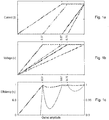
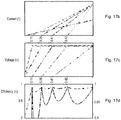
- the multistage Doherty amplifiers by Raab generally have their transition points too high to give good average efficiency with high-PAR signals if the transistor stages are of equal size.
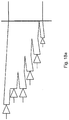
- Figures 1a, 1b and 1c show the curves for a 4-stage implementation, in which the lowest transition point is at 0.37 of full output.
- the amplifiers with higher numbers of stages generally have the same problem.
- the amplitude-limited drive signals required for best operation can sometimes pose a problem of increased implementation complexity.
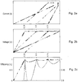
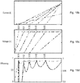
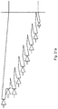
- the 4-stage amplifier of EP2,403,135 has an advantage in that the lowest transition point with four equal size transistors is at 0.25 of full output amplitude (-12 dB).
- the distribution of transition points is not so good for high-PAR signals, since the higher transition points are at too high output amplitudes, as shown in Figures 3a to 3c .
- An amplitude-limited drive signal is also required for this amplifier.
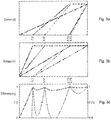
- Figures 3a to 3c relate to a 5-stage amplifier according to US8,022,760 .
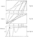
- Figures 4a to 4c relate to a 6-stage amplifier according to EP2,403,135 .
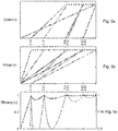
- Figures 5a to 5c relate to a 7-stage amplifier according to US8,022,760 .
- each of the amplifier arrangements described in Figures 3 , 4 and 5 have the disadvantage of requiring several (N-3) amplitude limited drive signals, and also have the disadvantage of having a poor distribution of transition points .
- an amplifier arrangement comprising N amplifier stages, wherein N is an integer equal or greater than four.
- the amplifier arrangement comprises a cascade of quarter wavelength transmission lines coupled between an output of an amplifier of a first amplifier stage and an output node of the amplifier arrangement, wherein the cascade comprises N-1 quarter wavelength transmission lines.
- An amplifier of the Nth stage is coupled to the output node, and remaining amplifiers between the first and the Nth stage coupled to successive junctions in the cascade of quarter wavelength transmission lines.
- the amplifier arrangement is further configured such that the coupling of the amplifier of the Nth stage to the output node is via a connecting quarter wavelength transmission line, and each coupling of the remaining amplifiers amongst the N-2 stages closest to the output node is via a respective connecting quarter wavelength transmission line to a respective junction of the cascade of quarter wavelength transmission lines.
- the amplifier of the second stage is directly coupled to its respective junction in the cascade of quarter wavelength transmission lines.
- An advantage of this arrangement is that it provides good efficiency for high PAR signals even with equal size transistors, due to a high density of transition points at low output amplitudes, as will be explained later in the application.
- an amplifier arrangement comprising N amplifier stages, wherein N is an integer equal or greater than four; wherein the amplifier arrangement comprises a cascade of quarter wavelength transmission lines coupled between an output of an amplifier of a first amplifier stage and an output node of the amplifier arrangement, wherein the cascade comprises N-1 quarter wavelength transmission lines, and wherein an amplifier of the Nth stage is coupled to the output node, and remaining amplifiers between the first and the Nth stage coupled to successive junctions in the cascade of quarter wavelength transmission lines.
- the method comprises the steps of: coupling the amplifier of the Nth stage to the output node via a connecting quarter wavelength transmission line; and coupling each of the remaining amplifiers in the N-2 stages closest to the output node via a respective connecting quarter wavelength transmission line to a respective junction of the cascade of quarter wavelength transmission lines; and coupling the amplifier of the second stage directly to its respective junction in the cascade of quarter wavelength transmission lines .
- Figure 6a shows an amplifier arrangement according to a first aspect of the present invention.
- the amplifier arrangement comprises 4 amplifier stages, 10 1 to 10 4 , although as will be described below the amplifier arrangement can comprise any higher number of amplifier stages, including both even and odd numbers of amplifier stages.
- the amplifier arrangement comprises a cascade of quarter wavelength transmission lines 11 1 to 11 3 coupled between an output of an amplifier of a first amplifier stage 10 1 and an output node 15 of the amplifier arrangement.
- the cascade comprises three quarter wavelength transmission lines 11 1 to 11 3 in this example.
- An amplifier of the 4th stage 10 4 is coupled to the output node, and remaining amplifiers between the 1 st and 4 th stages (amplifiers 10 2 and 10 3 in this example) are coupled to successive junctions in the cascade of quarter wavelength transmission lines 11 1 to 11 3 .
- the amplifier arrangement is configured such that the amplifier of the 4th stage 10 4 is coupled to the output node 15 via a connecting quarter wavelength transmission line 13 1 , with each of the remaining amplifiers closest to the output node 15 apart from the first and second amplifiers 10 1 ,10 2 (being just the amplifier of stage 10 3 in this particular example), being coupled by a respective connecting quarter wavelength transmission line (13 2 in this example) to a junction of the cascade of quarter wavelength transmission lines.
- the quarter wavelength transmission lines 11 1 to 11 3 are shown as having a decreasing characteristic impedance towards the output node 15 (represented by the comparative thickness of each quarter wavelength transmission line 11 1 to 11 3 ).
- the embodiments described herein will be described as having a cascade of quarter wavelength transmission lines with decreasing characteristic impedance towards the output node, it is noted that transformations may be provided in a network, as described later in the application, for providing the same effect as a deceasing characteristic impedance. The use of such transformations in the network might be beneficial when physical constraints are imposed on the amplifier arrangement, for example because of the physical size of the transmission lines required to give a particular characteristic impedance.
- the arrangement shown in Figure 6a can be used with an increasing number of amplifiers stages, for both odd and even numbers of amplifier stages N.
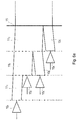
- Figure 6b describes this aspect of the invention for an amplifier arrangement comprising N amplifier stages, 10 1 to 10 N , wherein N is an integer equal or greater than four.
- the amplifier arrangement comprises a cascade of quarter wavelength transmission lines 11 1 to 11 N-1 coupled between an output of an amplifier of a first amplifier stage 10 1 and an output node 15 of the amplifier arrangement.
- the cascade comprises N-1 quarter wavelength transmission lines 11 1 to 11 N-1 .
- An amplifier of the Nth stage 10 N is coupled to the output node, and remaining amplifiers between the first and Nth stages 10 2 to 10 N-1 coupled to successive junctions in the cascade of quarter wavelength transmission lines 11 1 to 11 N-1 .
- the amplifier arrangement is configured such that the amplifier 10 N of the Nth stage is coupled to the output node 15 via a connecting quarter wavelength transmission line 13 1 , with each of the remaining amplifiers 10 3 to 10 N-1 of the N-2 stages closest to the output node 15 being coupled by a respective connecting quarter wavelength transmission line 13 1 to 13 N-2 to a junction of the cascade of quarter wavelength transmission lines.
- the cascade of N-1 quarter wavelength transmission lines 11 1 to 11 N-1 may comprise a decreasing characteristic impedance towards the output node.
- This arrangement has the advantage of providing good efficiency for high PAR signals even with equal size transistors, due to high density of transition points at low output amplitudes.
- embodiments of the present invention describe 4-stage and higher (“N-stage”) amplifier arrangements, and in particular a Doherty amplifier arrangement, whereby the N-2 amplifiers closest to the output are coupled by quarter wavelength lines to the junctions of the cascade of quarter wavelength lines (consisting of N-1 quarter wavelength lines of decreasing characteristic impedance towards the output, or equivalent transformations in a network).
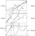
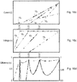
- Figure 6c shows a plot of current against output amplitude for the four-stage embodiment of the present invention as shown in Figure 6a .
- the order of the amplifier starting points in this example is amplifier 10 4 starting at zero, amplifier 10 3 starting at 0.25 of full output amplitude, amplifier 10 1 starting at 0.33 of full output amplitude, and amplifier 10 2 starting at 0.62 of full output amplitude.
- Figure 6d shows a plot of voltage against output amplitude for the four-stage embodiment of the present invention as shown in Figure 6a .
- Figure 6e shows a plot of efficiency against output amplitude for the four-stage embodiment of the present invention as shown in Figure 6a .
- the amplifier stages transistor, constituent amplifiers
- the quarterwave cascade junction one quarter wavelength from the output (i.e. amplifier 10 3 ) are connected via quarter wave lines.
- the quarterwave cascade itself contains three quarter wavelength lines, whereas the arrangement in prior art systems such as EP2403135 only have one quarterwave-connected stage, at the output, and a quarterwave cascade consisting of only two quarter wave lines.
- amplifiers 10 2 and 10 3 of the second and third amplifier stages are configured to have phase offsets of -90 degrees (a quarter RF cycle) relative to the phase of amplifier 10 4 of the fourth amplifier stage, and amplifier 10 1 of the first amplifier stage configured to have a phase offset of -180 degrees (a half RF cycle).
- the offsets can be implemented as time delays (which is also convenient for microwave implementations, where they can be implemented with transmission lines).
- each of the amplifiers in the amplifier stages (10 1 to 10 4 ) is of a substantially equal size.
- substantially equal size is meant that the amplifiers may be of the same generally type, or that the amplifiers may be configured to provide similar drive currents and/or voltages.
- the characteristic impedance of each successive stage in the cascade of quarter wavelength transmission lines 11 1 to 11 3 is reduced towards the output node, and in particular reduced to the parallel combination of the preceding connecting transmission lines.
- the characteristic impedance of each of the connecting quarter wavelength transmission lines 13 1 to 13 2 is substantially equal.
- the efficiency curve for such an amplifier arrangement designed for four equal size transistors has four peaks; at 0.25, 0.33, 0.62 and 1 of full output amplitude.
- Figure 6f shows a schematic diagram of the embodiment of Figure 6a , illustrated in an alternative manner. Similar schematic diagrams can be drawn for the other embodiments that are described below.
- Correctly tuned amplifiers have high, ideally infinite, impedance at the output. This high impedance is transformed by a quarterwave line so that the other end has a low (close to short circuit) impedance. Since the amplifier 10 4 of Figure 6a is connected by a quarterwave line to the output node 15, the output is thus short circuited when seen from amplifiers in the quarterwave cascade. In analogy with the traditional 2-stage Doherty amplifier, the amplifiers in the quarterwave cascade thus work together as an equivalent peaking amplifier to the fourth amplifier 10 4 , which consequentially works as a main, or carrier, amplifier.
- the amplifier 10 3 is connected by a quarterwave line to a junction in the quarterwave cascade. Therefore, this connection point is short circuited for RF voltage from the other amplifiers. These then act together as a peaking amplifier for the third amplifier 10 3 (i.e. "a peaking amplifier to the peaking amplifier”).
- the quarter wavelength transmission line of the first amplifier 10 1 short circuits the connection point for the second amplifier 10 2 , which in the same way acts as a peaking amplifier for the first amplifier 10 1 .
- the short circuiting of the connection points is the reason for the quarterwave cascade; a short circuited junction is displaced from the next by a quarter wavelength line that transforms the low impedance to an open circuit or high impedance.
- this scheme can be extended with good results to higher numbers of stages. This is achieved by using the N-stage amplifier, with the quarterwave cascade extended by an extra quarter wavelength (to the right), as the peaking amplifier for an (N+1)-stage. This is always possible, regardless of whether the starting N was even or odd. Higher order versions therefore exist for all numbers of stages, odd and even, contrary to prior art solutions. All higher order versions also have the advantageous property of having many transition points rather evenly distributed in the low amplitude range, for equal size transistors.
- the amplifier arrangement comprises a cascade of quarter wavelength transmission lines 11 1 to 11 4 coupled between an output of an amplifier of a first amplifier stage 10 1 and an output node 15 of the amplifier arrangement.
- the cascade comprises four (N-1) quarter wavelength transmission lines 11 1 to 11 4 of decreasing characteristic impedance towards the output node.
- An amplifier of the fifth stage 10 5 is coupled to the output node 15, and remaining amplifiers between the first and fifth stages, i.e. the amplifiers of stages 10 2 to 10 4 , coupled to successive junctions in the cascade of quarter wavelength transmission lines 11 1 to 11 4 .
- the amplifier arrangement is configured such that the amplifier 10 5 of the fifth stage is coupled to the output node 15 via a connecting quarter wavelength transmission line 13 1 , with each of the remaining amplifiers of the three stages closest to the output node 15 (i.e. amplifiers 10 3 and 10 4 in this example) being coupled by a respective connecting quarter wavelength transmission line 13 2 and 13 3 to a junction of the cascade of quarter wavelength transmission lines.
- Figure 8b shows a plot of current against output amplitude for the five-stage embodiment of the present invention as shown in Figure 8a .
- the order of the amplifier starting points in this example is amplifier 10 5 starting at zero, amplifier 10 4 starting at 0.2 of full output amplitude, amplifier 10 3 starting at 0.25 of full output amplitude, amplifier 10 1 starting at 0.47 of full output amplitude, and amplifier 10 2 starting at 0.62 of full output amplitude.
- Figure 8c shows the voltages of the respective amplifier stages 10 1 to 10 5 relative to full output amplitude.
- the efficiency curve for an amplifier designed for five equal size transistors has five peaks; at 0.20, 0.25, 0.47, 0.62 and 1 of full output amplitude.
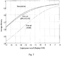
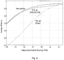
- This distribution of transition points is advantageous for high-PAR signals, and better that the prior art solutions for all relevant Rayleigh PAR values, as shown in Figure 9 .
- the amplifier arrangement comprises a cascade of quarter wavelength transmission lines 11 1 to 11 5 coupled between an output of an amplifier of a first amplifier stage 10 1 and an output node 15 of the amplifier arrangement.
- the cascade comprises five (N-1) quarter wavelength transmission lines 11 1 to 11 5 of decreasing characteristic impedance towards the output node.
- An amplifier of the sixth stage 10 6 is coupled to the output node 15, and remaining amplifiers between the first and sixth stages, i.e. the amplifiers of stages 10 2 to 10 5 in this example, coupled to successive junctions in the cascade of quarter wavelength transmission lines 11 1 to 11 5 .
- the amplifier arrangement is configured such that the amplifier 10 6 of the sixth stage is coupled to the output node 15 via a connecting quarter wavelength transmission line 13 1 , with each of the remaining amplifiers of the four stages closest to the output node 15 (i.e. amplifiers 10 3 to 10 5 in this example) being coupled by a respective connecting quarter wavelength transmission line 13 2 to 13 4 to a junction of the cascade of quarter wavelength transmission lines.
- Figure 10b shows a plot of current against output amplitude for the six-stage embodiment of the present invention as shown in Figure 10a .
- the order of the amplifier starting points in this example is amplifier 10 6 starting at zero, amplifier 10 5 starting at 0.17 of full output amplitude, amplifier 10 4 starting at 0.2 of full output amplitude, amplifier 10 3 starting at 0.37 of full output amplitude, amplifier 10 1 starting at 0.47 of full output amplitude, and amplifier 10 2 starting at 0.69 of full output amplitude.
- Figure 10c shows the voltages of the respective amplifier stages 10 1 to 10 6 relative to full output amplitude.
- this shows the efficiency curve, using six transistors of substantially equal size, having six peaks; at 0.17, 0.20, 0.37, 0.47, 0.69 and 1 of full output amplitude.
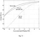
- This distribution of transition points is advantageous for high-PAR signals, and improved compared to the prior art solutions for essentially all Rayleigh PAR values, as shown in Figure 11 .
- Embodiments for an increasing number of amplifier stages can be configured in a similar manner to the embodiments of Figures 6a , 8a , and 10a .
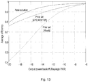
- Figure 12 compares the efficiency of a 7-stage amplifier arrangement with prior art solutions (all designed for substantially equal sized transistors or amplifiers).
- Figure 13 compares the efficiency of a 8-stage amplifier arrangement with prior art solutions (all designed for substantially equal sized transistors or amplifiers).
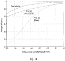
- Figure 14 compares the efficiency of a 9-stage amplifier arrangement with prior art solutions (all designed for substantially equal sized transistors or amplifiers).
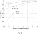
- Figure 15 compares the efficiency of a 10-stage amplifier arrangement with prior art solutions (all designed for substantially equal sized transistors or amplifiers).
- the embodiments of the invention thus perform generally better than prior art Doherty amplifiers in relation to average efficiency for high-PAR signals. It is noted that the relative advantage increases with increasing numbers of amplifier stages.
- the transition points at which amplifier stages switch into operation can be distributed more evenly.
- This improved distribution of transition points may be achieved by making the starting amplifier, i.e. the transistor closest to the output (the Nth amplifier stage of the embodiments described above), smaller compared to the others.
- the Nth amplifier is made about half the size (e.g. half the output current rating) compared to the remaining amplifiers.
- the connecting quarter wavelength transmission line 13 1 from the Nth amplifier 10 N i.e. from 10 4
- the characteristic impedance of the corresponding connecting quarter wavelength transmission line can be twice the characteristic impedance of the other connecting quarter wavelength transmission lines.
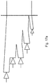
- Figure 16a shows such a configuration for a 4-stage amplifier, although it is noted that this aspect can be used with any number of stages of four and above.
- Figure 16a shows an amplifier arrangement comprising four amplifier stages, 10 1 to 10 4 , and a cascade of quarter wavelength transmission lines 11 1 to 11 3 coupled between an output of an amplifier of a first amplifier stage 10 1 and an output node 15 of the amplifier arrangement.
- the cascade comprises three quarter wavelength transmission lines 11 1 to 11 3 in this example, of decreasing characteristic impedance towards the output node.
- An amplifier of the 4th stage 10 4 is coupled to the output node, and remaining amplifiers between the 1 st and 3rd stages (amplifiers 10 2 and 10 3 in this example) are coupled to successive junctions in the cascade of quarter wavelength transmission lines 11 1 to 11 3 .
- the amplifier arrangement is configured such that the amplifier of the 4th stage 10 4 is coupled to the output node 15 via a connecting quarter wavelength transmission line 13 1 , with each of the remaining amplifiers closest to the output node 15 apart from the first and second amplifiers 10 1 , 10 2 (being just the amplifier of stage 10 3 in this example), being coupled by a respective connecting quarter wavelength transmission line (13 2 in this example) to a junction of the cascade of quarter wavelength transmission lines.
- the amplifier in the Nth amplifier stage 10 N (closest to the output node), i.e. the fourth amplifier 10 4 , is reduced in size compared to the other amplifiers in the other amplifier stages 10 1 to 10 N-1
- the characteristic impedance of the connecting quarter wavelength transmission line 13 1 coupling the amplifier in the Nth amplifier stage to the output node is increased by a corresponding ratio compared to the characteristic impedance of each of the other connecting quarter wavelength transmission lines 13 2 to 13 N-2 , (i.e. compared to 13 2 in this example).
- the amplifier in the Nth amplifier stage 10 N is substantially halved in size compared to the other amplifiers in the other amplifier stages 10 1 to 10 N-1 , and wherein the characteristic impedance of the connecting quarter wavelength transmission line 13 1 coupling the amplifier in the Nth stage to the output node is substantially doubled in size compared to the characteristic impedance of each of the other connecting quarter wavelength transmission lines 13 2 to 13 N-2 .
- Figure 16c shows the voltages of the respective amplifier stages 10 1 to 10 4 relative to full output amplitude.
- the efficiency curve for such an amplifier designed for four amplifier stages with the closest to the output being smaller in size has four peaks; at 0.14, 0.33, 0.57, 0.62 and 1 of full output amplitude.
- This distribution of transition points is advantageous for high-PAR signals, and better that the prior art solutions for all relevant Rayleigh PAR values. In particular, such an evenly distribution of transition points would generally require more different sizes of transistors if prior art Doherty amplifiers were used.
- another way to achieve a more even distribution of efficiency peaks is by increasing the size of the amplifier second closest to the output (also known as the "first peaking amplifier") relative to the other amplifiers, For example, according to one embodiment this amplifier may be increased by 25-50% relative to the other amplifiers. In such an embodiment the characteristic impedance of the respective connecting quarter wavelength transmission line 13 2 is decreased by some corresponding function (as illustrated by the increased comparative thickness of 13 2 ).
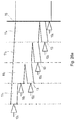
- Figure 23a shows such a configuration for a 5-stage amplifier, although it is noted that this aspect can be used with any number of stages of four and above.
- Figure 23a shows an amplifier arrangement comprising five amplifier stages, 10 1 to 10 5 , and a cascade of quarter wavelength transmission lines 11 1 to 11 4 coupled between an output of an amplifier of a first amplifier stage 10 1 and an output node 15 of the amplifier arrangement.
- the cascade comprises four quarter wavelength transmission lines 11 1 to 11 4 in this example, of decreasing characteristic impedance towards the output node.
- An amplifier of the 5th stage 10 5 is coupled to the output node, and remaining amplifiers between the 1 st and 4th stages (amplifiers 10 2 ,10 3 and 10 4 in this example) are coupled to successive junctions in the cascade of quarter wavelength transmission lines 11 1 to 11 4 .
- the amplifier arrangement is configured such that the amplifier of the 5th stage 10 5 is coupled to the output node 15 via a connecting quarter wavelength transmission line 13 1 , with each of the remaining amplifiers closest to the output node 15 apart from the first and second amplifiers 10 1 , 10 2 , (being the amplifiers of stages 10 3 and 10 4 in this example), being coupled by a respective connecting quarter wavelength transmission line (13 2 , 13 3 in this example) to a junction of the cascade of quarter wavelength transmission lines.
- each of the amplifiers in the N amplifier stages is of a substantially equal size apart from an amplifier in the N-1 amplifier stage 10 N-1 (i.e. 10 4 ) that is second closest to the output node, wherein the amplifier in this 4 th stage is increased in size relative to the amplifiers in the other stages 10 1 to 10 N-2 , 10 N (i.e. amplifiers 10 1 to 10 3 , 10 5 in this example).
- the amplifier in the N-1 stage 10 N-1 (i.e. the amplifier of the 4 th stage 10 4 in this example) is increased in size compared to the other amplifiers in the other amplifier stages, and wherein the characteristic impedance of the connecting quarter wavelength transmission line 13 2 coupling the amplifier in the N-1 stage (4 th stage in this example) to the cascade is decreased compared to the characteristic impedance of each of the other connecting quarter wavelength transmission lines 13 1 , 13 3 to 13 N-2 (13 1 and 13 3 in this example).
- the amplifier in the 4 th stage 10 4 is increased by about 25-50% in size compared to the other amplifiers in the other amplifier stages (10 1 to 10 3 , 10 N ), and wherein the characteristic impedance of the connecting quarter wavelength transmission line (13 2 ) coupling the amplifier in the 4 th stage to the cascade is substantially decreased by about 20-50% compared to the characteristic impedance of each of the other connecting quarter wavelength transmission lines (13 1 and 13 3 ).
- the amplifier in the 4 th stage can be about 30% larger than the other amplifiers, and the characteristic impedance of its connecting quarter wavelength transmission line correspondingly 23 % lower than for the rest of the connecting quarter wavelength transmission lines.
- Figure 23c shows the voltages of the respective amplifier stages 10 1 to 10 5 relative to full output amplitude.
- the efficiency curve for such an amplifier designed for five amplifier stages with the stage second closest to the output being larger in size has five peaks; at 0.19, 0.3, 0.46, 0.65 and 1 of full output amplitude.
- This distribution of transition points is advantageous for high-PAR signals, and better that the prior art solutions for all relevant Rayleigh PAR values. In particular, such an even distribution of transition points would generally require more different sizes of transistors if prior art Doherty amplifiers were used.
- Figure 23a may be used in combination with one or more of the other embodiments described herein. For example, increasing the impedance of the last quarterwave line, for example by 33%, and reducing the size of the amplifier, for example to 75%, and reducing the impedance of the second last line, for example by 13%, and increasing the size of the corresponding amplifier, for example by 15%.
- the size of the last peaking amplifier (the amplifier of the second stage 10 2 ) can be increased, such that the entire set of efficiency peaks can be translated to lower amplitudes, and with retained evenness.
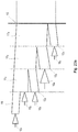
- Figure 24a shows an amplifier arrangement comprising 6 amplifier stages, 10 1 to 10 6 , and a cascade of quarter wavelength transmission lines 11 1 to 11 5 coupled between an output of an amplifier of a first amplifier stage 10 1 and an output node 15 of the amplifier arrangement.
- the cascade comprises five quarter wavelength transmission lines 11 1 to 11 5 in this example, of decreasing characteristic impedance towards the output node.
- An amplifier of the 6th stage 10 6 is coupled to the output node, and remaining amplifiers between the 1 st and 6th stages (amplifiers 10 2 to 10 5 in this example) are coupled to successive junctions in the cascade of quarter wavelength transmission lines 11 1 to 11 5 .
- the amplifier arrangement is configured such that the amplifier of the 6th stage 10 6 is coupled to the output node 15 via a connecting quarter wavelength transmission line 13 1 , with each of the remaining amplifiers closest to the output node 15 apart from the first and second amplifiers 10 1 ,10 2 (being the amplifiers of stages 10 3 , 10 4 and 10 5 in this example), being coupled by a respective connecting quarter wavelength transmission line (13 2 , 13 3 and 13 4 in this example) to a junction of the cascade of quarter wavelength transmission lines.
- the amplifier in the second stage 10 2 is increased or decreased compared to the other amplifiers in at least the first to N-2 other amplifier stages 10 1 , 10 3 to 10 N-2 , (i.e. compared to at least the amplifiers 10 1 and 10 3 to 10 4 in this example), and the characteristic impedance decreased or increased in a corresponding manner.
- this amplifier By increasing the size of this amplifier in the second stage 10 2 , effectively the last peaking amplifier, this causes the entire set of efficiency peaks to be translated to lower amplitudes, with retained evenness. Likewise, decreasing the size of this amplifier causes the whole bunch of efficiency peaks to be translated to higher amplitudes, also with retained evenness
- Figure 24b shows how the transition points have been shifted to occur at 0.06, 0.12, 0.19, 0.27 and 0.35 of full output amplitude, while maintaining the more evenly spread compared to other embodiment.
- Figure 24b shows the voltages of the respective amplifier stages 10 1 to 10 6 relative to full output amplitude.
- the efficiency curve for such an amplifier designed for six amplifier stages with the stage second closest to the input being larger in size has six peaks; at 0.06, 0.12, 0.19, 0.27, 0.35 and 1 of full output amplitude.
- This distribution of transition points is advantageous for high-PAR signals, and better that the prior art solutions for all relevant Rayleigh PAR values.
- the amplifier of the second stage is four times as large as the four 'middle' amplifiers.
- This efficiency peak shift can be made larger or smaller without disturbing the evenness of the efficiency peaks.
- a shift in the other direction is achieved by making the transistor smaller instead. Also in this case the evenness of the efficiency peak distribution is retained.
- Figure 24a may be used in combination with any one or more of the other embodiments described herein. For example, increasing the impedance of the last quarterwave line, for example by 33%, and reducing the size of the amplifier, for example to 75%, and reducing the impedance of the second last line, for example by 13%, and increasing the size of the corresponding amplifier, for example by 15%.
- any quarterwave line can double as an impedance transformer, i.e. the impedance and corresponding maximum RF voltage swings can be individually adjusted for each transistor. This can be useful if one or more of the transistors are made with a different technology having a different voltage rating. It can also be beneficial to use these transformations to accommodate a different load impedance, instead of making this transformation outside of the Doherty amplifier which would require extra impedance transformers. Apart from these considerations, it can be advantageous to have as little extra impedance transformations as possible in the Doherty network, since this generally gives high bandwidth and low sensitivity.
- the actual shapes may have to take into account that the voltage-to-current conversion (transconductance) in the transistors is more or less nonlinear, and that the RF voltage swing can influence the output current as well (especially via saturation when close to the upper limit).
- Causing a transistor to turn on at a higher amplitude is often done by lowering the gate bias to the transistor, i.e. operating in class C. This means that less large-scale amplitude shaping needs to be done earlier in the processing chain, but usually at the cost of lower gain and lower maximum output power.
- any of the transmission lines in the examples described herein can be wholly or partially replaced by combinations of lumped elements.
- the quarterwave lines can be replaced by LC pi- or T-networks with inductors (L) and capacitors (C) with reactances equal in magnitude to the characteristic impedance of the replaced quarterwave line.
- the embodiments of the invention provide advantageous Doherty amplifiers with four or more stages. For high PAR signals, the distribution of transition points when equal size transistors are used is improved compared to prior art Doherty amplifiers.
- the efficiency peaks can be distributed even more evenly, which increases average efficiency for high-PAR signals.
- the size of another transistor for example the second amplifier stage
- the whole bunch of efficiency peaks can be moved to higher or lower amplitude ranges, with retained evenness. Good dimensioning is thus easily achieved.
- Figure 25 shows a method of improving the efficiency of an amplifier arrangement comprising N amplifier stages 10 1 to 10 N , wherein N is an integer equal or greater than four, wherein the amplifier arrangement comprises a cascade of quarter wavelength transmission lines coupled between an output of an amplifier of a first amplifier stage 10 1 and an output node 15 of the amplifier arrangement, wherein the cascade comprises N-1 quarter wavelength transmission lines 11 1 to 11 N-1 , and wherein an amplifier of the Nth stage 10 N is coupled to the output node 15, and remaining amplifiers between the first and Nth stages 10 2 to 10 N-1 coupled to successive junctions in the cascade of quarter wavelength transmission lines 11 1 to 11 N-1 .
- the method comprises the steps of coupling the amplifier of the Nth stage 10 N to the output node 15 via a connecting quarter wavelength transmission line 13 1 , step 2501.
- Each of the remaining amplifiers 10 3 to 10 N-1 in the N-2 stages closest to the output node 15 is coupled by a respective connecting quarter wavelength transmission line 13 2 to 13 N-2 to a junction of the cascade of quarter wavelength transmission lines, step 2503.
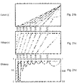
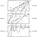
- Figure 26a shows an amplifier arrangement according to another aspect, with Figures 26b to 26d showing current, voltage and efficiency curves for the amplifier arrangement of Figure 26a .
- the arrangement of Figure 26a is a six-stage amplifier arrangement similar to that of Figure 10a .
- the Nth amplifier 10 6 is coupled directly to the output node 15, rather than via a connecting transmission line as provided in Figure 10a .
- the cascade of quarter wavelength transmission lines comprises N-2 stages, i.e. 11 1 to 11 4 , rather than N-1 stages as provided in Figure 10a .
- the amplifier arrangement comprises a cascade of quarter wavelength transmission lines 11 1 to 11 4 coupled between an output of an amplifier of a first amplifier stage 10 1 and an output node 15 of the amplifier arrangement.
- the cascade comprises four (N-2) quarter wavelength transmission lines 11 1 to 11 4 of decreasing characteristic impedance towards the output node.
- An amplifier of the sixth stage 10 6 is coupled to the output node 15, and remaining amplifiers between the first and sixth stages, i.e. the amplifiers of stages 10 2 to 10 5 in this example, coupled to successive junctions in the cascade of quarter wavelength transmission lines 11 1 to 11 4 .
- the amplifier arrangement is configured such that the amplifier 10 6 of the sixth stage is coupled directly to the output node 15, with each of the remaining amplifiers of the four stages closest to the output node 15 (i.e. amplifiers 10 3 to 10 5 in this example) being coupled by a respective connecting quarter wavelength transmission line 13 to a junction of the cascade of quarter wavelength transmission lines.
- Figure 26b shows a plot of current against output amplitude for the six-stage arrangement as shown in Figure 26a .
- the order of the amplifier starting points in this example is amplifier 10 5 starting at zero, amplifier 10 4 starting at 0.17 of full output amplitude, amplifier 10 3 starting at 0.25 of full output amplitude, amplifier 10 1 starting at 0.39 of full output amplitude, amplifier 10 2 starting at 0.62 of full output amplitude, and amplifier 10 6 starting at 0.83 of full output amplitude.
- Figure 26c shows the voltages of the respective amplifier stages 10 1 to 10 6 relative to full output amplitude.
- this shows the efficiency curve, using six transistors of substantially equal size, having six peaks; at 0.17, 0.25, 0.39, 0.62, 0.83 and 1 of full output amplitude.
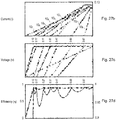
- Figure 27a shows an amplifier arrangement according to another aspect, with Figures 27b to 27d showing current, voltage and efficiency curves for the amplifier arrangement of Figure 27a .
- the arrangement of Figure 27a is an example of a eight-stage amplifier arrangement.
- the Nth amplifier 10 8 is coupled directly to the output node 15, rather than via a connecting quarter wavelength transmission line.
- the cascade of quarter wavelength transmission lines comprises N-2 stages, i.e. 11 1 to 11 6 , rather than N-1 stages as provided in the earlier embodiments.
- the amplifier arrangement comprises a cascade of quarter wavelength transmission lines 11 1 to 11 6 coupled between an output of an amplifier of a first amplifier stage 10 1 and an output node 15 of the amplifier arrangement.
- the cascade comprises six (N-2) quarter wavelength transmission lines 11 1 to 11 6 of decreasing characteristic impedance towards the output node.
- An amplifier of the sixth stage 10 6 is coupled to the output node 15, and remaining amplifiers between the first and sixth stages, i.e. the amplifiers of stages 10 2 to 10 5 in this example, coupled to successive junctions in the cascade of quarter wavelength transmission lines 11 1 to 11 4 .
- the amplifier arrangement is configured such that the amplifier 10 8 of the eighth stage is coupled directly to the output node 15, with each of the remaining amplifiers of the six stages closest to the output node 15 (i.e. amplifiers 10 3 to 10 7 in this example) being coupled by a respective connecting quarter wavelength transmission line 13 to a junction of the cascade of quarter wavelength transmission lines.
- Figure 27b shows a plot of current against output amplitude for the eight-stage arrangement as shown in Figure 27a .
- the order of the amplifier starting points in this example is amplifier 10 7 starting at zero, amplifier 10 6 starting at 0.12 of full output amplitude, amplifier 10 5 starting at 0.17 of full output amplitude, amplifier 10 4 starting at 0.27 of full output amplitude, amplifier 10 3 starting at 0.37 of full output amplitude amplifier, 10 1 starting at 0.47 of full output amplitude, amplifier 10 2 starting at 0.69 of full output, and amplifier 10 8 starting at 0.87 of full output amplitude.
- Figure 27c shows the voltages of the respective amplifier stages 10 1 to 10 8 relative to full output amplitude.
- this shows the efficiency curve, using eight transistors of substantially equal size, having six peaks; at 0.12, 0.17, 0.27, 0.37, 0.47, 0.69, 0.87 and 1 of full output amplitude.
Landscapes
- Engineering & Computer Science (AREA)
- Power Engineering (AREA)
- Microelectronics & Electronic Packaging (AREA)
- Amplifiers (AREA)
- Microwave Amplifiers (AREA)
Claims (15)
- Agencement amplificateur comprenant N étages amplificateurs (101 à 10N), dans lequel N est un nombre entier égal ou supérieur à quatre; l'agencement amplificateur comprenant :une cascade de lignes de transmission quart d'onde couplées entre une sortie d'un amplificateur d'un premier étage amplificateur (101) et un nœud de sortie (15) de l'agencement amplificateur, dans lequel la cascade comprend N-1 lignes de transmission quart d'onde (111 à 11N-1) ;dans lequel un amplificateur du Nième étage (10N) est couplé au nœud de sortie (15), et des amplificateurs restants entre le premier et le Nième étage (102 à 10N-1) sont couplés à des jonctions successives dans la cascade de lignes de transmission quart d'onde (111 à 11N-1) ; etdans lequel l'agencement amplificateur est configuré en outre de telle sorte que :le couplage de l'amplificateur du Nième étage (10N) au nœud de sortie (15) se fait par l'intermédiaire d'une ligne de transmission quart d'onde de liaison (131) ; etchaque couplage des amplificateurs restants parmi les N-2 étages (103 à 10N-1) les plus proches du nœud de sortie (15) se fait par l'intermédiaire d'une ligne de transmission quart d'onde de liaison respective (132 à 13N-2) à une jonction respective de la cascade de lignes de transmission quart d'onde ; etun amplificateur du deuxième étage (102) est couplé directement à sa jonction respective dans la cascade de lignes de transmission quart d'onde (111 à 11N-1).
- Amplificateur selon la revendication 1, dans lequel chacun des amplificateurs des N étages amplificateurs (101 à 10N) est d'une taille égale.
- Amplificateur selon les revendications 1 ou 2, dans lequel une impédance caractéristique de chaque étage successif dans la cascade de lignes de transmission quart d'onde (111 à 11N-1) est réduite vers le nœud de sortie par rapport à la combinaison parallèle de lignes de transmission de liaison précédentes, moyennant quoi l'impédance caractéristique de chaque étage successif est réduite à 1/M de l'impédance de la ligne de transmission provenant d'un seul amplificateur, M se rapportant au nombre d'amplificateurs précédents.
- Amplificateur selon l'une quelconque des revendications 1 à 3, dans lequel l'impédance caractéristique de chacune des lignes de transmission quart d'onde de liaison (131 à 13N-2) est égale.
- Amplificateur selon la revendication 1, dans lequel chacun des amplificateurs des premier à N-1 étages amplificateurs (101 à 10N-1) est d'une taille égale, et
dans lequel l'amplificateur du Nième étage amplificateur (10N) qui est le plus proche du nœud de sortie (15) présente une taille différente de celles des autres amplificateurs. - Amplificateur selon la revendication 5, dans lequel l'amplificateur du Nième étage amplificateur (10N) présente une taille réduite par rapport à celle des autres amplificateurs des autres étages amplificateurs (101 à 10N-1), et dans lequel l'impédance caractéristique de la ligne de transmission quart d'onde de liaison (131) couplant l'amplificateur du Nième étage amplificateur au nœud de sortie est augmentée d'un rapport correspondant par rapport à l'impédance caractéristique de chacune des autres lignes de transmission quart d'onde de liaison (132 à 13N-2).
- Amplificateur selon la revendication 6, dans lequel la taille de l'amplificateur du Nième étage amplificateur (10N) est sensiblement réduite de moitié par rapport à celle des autres amplificateurs des autres étages amplificateurs (101 à 10N-1), et dans lequel l'impédance caractéristique de la ligne de transmission quart d'onde de liaison (131) couplant l'amplificateur du Nième étage au nœud de sortie est sensiblement doublée par rapport à l'impédance caractéristique de chacune des autres lignes de transmission quart d'onde de liaison (132 à 13N-2).
- Amplificateur selon la revendication 1, dans lequel chacun des amplificateurs des N étages amplificateurs (101 à 10N) est d'une taille sensiblement égale à l'exception d'un amplificateur de l'étage amplificateur N-1 (10N-1) qui est le suivant le plus proche du nœud de sortie, dans lequel la taille de l'amplificateur de l'étage N-1 est augmentée par rapport à celle des amplificateurs des autres étages (101 à 10N-2, 10N).
- Amplificateur selon la revendication 8, dans lequel la taille de l'amplificateur de l'étage N-1 (10N-1) est augmentée par rapport à celle des autres amplificateurs des autres étages amplificateurs, et dans lequel l'impédance caractéristique de la ligne de transmission quart d'onde de liaison (132) couplant l'amplificateur de l'étage N-1 à la cascade est diminuée par rapport à l'impédance caractéristique de chacune des autres lignes de transmission quart d'onde de liaison (131, 133 à 13N-2).
- Amplificateur selon la revendication 9, dans lequel la taille de l'amplificateur de l'étage N-1 (10N-1) est augmentée d'environ 25-50 % par rapport à celle des autres amplificateurs des autres étages amplificateurs (101 à 10N-2, 10N), et dans lequel l'impédance caractéristique de la ligne de transmission quart d'onde de liaison (132) couplant l'amplificateur de l'étage N-1 à la cascade est sensiblement diminuée d'environ 20-50 % par rapport à l'impédance caractéristique de chacune des autres lignes de transmission quart d'onde de liaison (131, 133 à 13N-2).
- Amplificateur selon l'une quelconque des revendications précédentes, dans lequel la taille de l'amplificateur du deuxième étage (102) est augmentée ou diminuée par rapport à celle des autres amplificateurs au moins des premier à N-2 autres étages amplificateurs (101, 103 à 10N-2), et l'impédance caractéristique diminuée ou augmentée d'une manière correspondante.
- Procédé d'amélioration de l'efficacité d'un agencement amplificateur comprenant N étages amplificateurs (101 à 10N), dans lequel N est un nombre entier égal ou supérieur à quatre; dans lequel l'agencement amplificateur comprend une cascade de lignes de transmission quart d'onde couplées entre une sortie d'un amplificateur d'un premier étage amplificateur (101) et un nœud de sortie (15) de l'agencement amplificateur, dans lequel la cascade comprend N-1 lignes de transmission quart d'onde (111 à 11N-1), et dans lequel un amplificateur du Nième étage (10N) est couplé au nœud de sortie (15), et des amplificateurs restants entre le premier et le Nième étage (102 à 10N-1) sont couplés à des jonctions successives dans la cascade de lignes de transmission quart d'onde (111 à 11N-1) ; le procédé comprenant les étapes suivantes :couplage de l'amplificateur du Nième étage (10N) au nœud de sortie (15) par l'intermédiaire d'une ligne de transmission quart d'onde de liaison (131) ;couplage de chacun des amplificateurs restants (103 à 10N-1) des N-2 étages (103 à 10N-1) les plus proches du nœud de sortie (15) par l'intermédiaire d'une ligne de transmission quart d'onde de liaison respective (132 à 13N-2) à une jonction respective de la cascade de lignes de transmission quart d'onde ; etcouplage d'un amplificateur du deuxième étage (102) directement à sa jonction respective dans la cascade de lignes de transmission quart d'onde (111 à 11N-1).
- Procédé selon la revendication 12, dans lequel chacun des amplificateurs des N étages amplificateurs (101 à 10N) est d'une taille égale.
- Procédé selon les revendications 12 ou 13, comprenant en outre l'étape de réduction d'une impédance caractéristique de chaque étage successif dans la cascade de lignes de transmission quart d'onde (111 à 11N-1) vers le nœud de sortie par rapport à la combinaison parallèle de lignes de transmission de liaison précédentes, moyennant quoi l'impédance caractéristique de chaque étage successif est réduite à 1/M de l'impédance de la ligne de transmission provenant d'un seul amplificateur, M se rapportant au nombre d'amplificateurs précédents.
- Procédé selon l'une quelconque des revendications 12 à 14, dans lequel l'impédance caractéristique de chacune des lignes de transmission quart d'onde de liaison (131 à 13N-2) est égale.
Applications Claiming Priority (1)
| Application Number | Priority Date | Filing Date | Title |
|---|---|---|---|
| PCT/EP2013/063732 WO2014206502A1 (fr) | 2013-06-28 | 2013-06-28 | Circuit amplificateur et procédé |
Publications (2)
| Publication Number | Publication Date |
|---|---|
| EP3014764A1 EP3014764A1 (fr) | 2016-05-04 |
| EP3014764B1 true EP3014764B1 (fr) | 2019-11-27 |
Family
ID=48874251
Family Applications (1)
| Application Number | Title | Priority Date | Filing Date |
|---|---|---|---|
| EP13740219.4A Active EP3014764B1 (fr) | 2013-06-28 | 2013-06-28 | Circuit d'amplificateur et methode correspondante |
Country Status (3)
| Country | Link |
|---|---|
| US (1) | US9853604B2 (fr) |
| EP (1) | EP3014764B1 (fr) |
| WO (1) | WO2014206502A1 (fr) |
Families Citing this family (5)
| Publication number | Priority date | Publication date | Assignee | Title |
|---|---|---|---|---|
| WO2014206501A1 (fr) | 2013-06-28 | 2014-12-31 | Telefonaktiebolaget L M Ericsson (Publ) | Circuit amplificateur et procédé |
| WO2015139745A1 (fr) | 2014-03-19 | 2015-09-24 | Telefonaktiebolaget L M Ericsson (Publ) | Circuit amplificateur et procédé |
| US9954492B2 (en) | 2014-03-19 | 2018-04-24 | Telefonaktiebolaget Lm Ericsson (Publ) | Amplifier circuit and method |
| WO2015150873A1 (fr) | 2014-04-03 | 2015-10-08 | Telefonaktiebolaget L M Ericsson (Publ) | Amplificateurs à plusieurs étages à faible perte |
| JP6608959B2 (ja) * | 2015-05-12 | 2019-11-20 | テレフオンアクチーボラゲット エルエム エリクソン(パブル) | 複合電力増幅器 |
Family Cites Families (10)
| Publication number | Priority date | Publication date | Assignee | Title |
|---|---|---|---|---|
| US5025225A (en) | 1989-12-15 | 1991-06-18 | Raytheon Company | Amplifier having substantially constant D.C. to r.f. conversion efficiency |
| US6472934B1 (en) * | 2000-12-29 | 2002-10-29 | Ericsson Inc. | Triple class E Doherty amplifier topology for high efficiency signal transmitters |
| KR20060077818A (ko) * | 2004-12-31 | 2006-07-05 | 학교법인 포항공과대학교 | 비대칭 전력 구동을 이용한 전력 증폭 장치 |
| JP5001435B2 (ja) | 2007-12-21 | 2012-08-15 | エヌエックスピー ビー ヴィ | 出力回路網を最小にした3ウェイドハティ増幅器 |
| EP2403135B1 (fr) | 2010-06-24 | 2013-12-11 | Alcatel Lucent | Amplificateur de puissance pour télécommunication mobile |
| EP2579457B1 (fr) * | 2011-09-06 | 2014-11-12 | Alcatel Lucent | Amplificateur de puissance pour télécommunications mobiles |
| US9374041B2 (en) * | 2011-12-15 | 2016-06-21 | Telefonaktiebolaget Lm Ericsson (Publ) | Doherty power amplification apparatus and method |
| EP2608400B1 (fr) | 2011-12-20 | 2014-08-13 | Nxp B.V. | Amplificateur de Doherty à n chemins |
| CN103178786A (zh) * | 2011-12-26 | 2013-06-26 | 瑞典爱立信有限公司 | 多路Doherty放大器 |
| US8653889B1 (en) * | 2012-09-06 | 2014-02-18 | Alcatel Lucent | Doherty amplifier having compact output matching and combining networks |
-
2013
- 2013-06-28 EP EP13740219.4A patent/EP3014764B1/fr active Active
- 2013-06-28 WO PCT/EP2013/063732 patent/WO2014206502A1/fr not_active Ceased
- 2013-06-28 US US14/900,726 patent/US9853604B2/en not_active Expired - Fee Related
Non-Patent Citations (1)
| Title |
|---|
| None * |
Also Published As
| Publication number | Publication date |
|---|---|
| EP3014764A1 (fr) | 2016-05-04 |
| US20160149541A1 (en) | 2016-05-26 |
| US9853604B2 (en) | 2017-12-26 |
| WO2014206502A1 (fr) | 2014-12-31 |
Similar Documents
| Publication | Publication Date | Title |
|---|---|---|
| EP3120454B1 (fr) | Circuit amplificateur et procédé | |
| EP3014764B1 (fr) | Circuit d'amplificateur et methode correspondante | |
| EP2690779A2 (fr) | Systèmes d'amplificateur de puissance AFT à large bande avec équilibrage d'impédance du transformateur de sortie basé sur la fréquence | |
| EP3205015B1 (fr) | Circuit amplificateur et procédé | |
| CN108352816B (zh) | 分布式功率放大器 | |
| CN103391057A (zh) | 一种逆f类功率放大器、发射器及处理方法 | |
| US9712118B2 (en) | Amplifier circuit and method | |
| WO2014132645A1 (fr) | Circuit d'adaptation variable et amplificateur | |
| US9768735B2 (en) | Amplifier circuit and method | |
| US10270396B2 (en) | Push-pull amplification systems and methods | |
| CN108847825B (zh) | 晶体管推挽对及具有该推挽对结构的射频放大电路 | |
| EP3205016B1 (fr) | Circuit amplificateur et procédé | |
| US9954492B2 (en) | Amplifier circuit and method | |
| JP4739717B2 (ja) | 歪補償回路 | |
| US9577584B2 (en) | Amplifier circuit and method | |
| EP3607657B1 (fr) | Agencement d'amplificateur de puissance à large bande | |
| Arya et al. | Designing and Optimization to the Performance of Multi Stage Tuned Amplifier | |
| HK40013554B (en) | Wideband power amplifier arrangement | |
| JP2019029974A (ja) | 増幅器、無線機及び高調波処理方法 |
Legal Events
| Date | Code | Title | Description |
|---|---|---|---|
| PUAI | Public reference made under article 153(3) epc to a published international application that has entered the european phase |
Free format text: ORIGINAL CODE: 0009012 |
|
| 17P | Request for examination filed |
Effective date: 20151124 |
|
| AK | Designated contracting states |
Kind code of ref document: A1 Designated state(s): AL AT BE BG CH CY CZ DE DK EE ES FI FR GB GR HR HU IE IS IT LI LT LU LV MC MK MT NL NO PL PT RO RS SE SI SK SM TR |
|
| AX | Request for extension of the european patent |
Extension state: BA ME |
|
| DAX | Request for extension of the european patent (deleted) | ||
| STAA | Information on the status of an ep patent application or granted ep patent |
Free format text: STATUS: EXAMINATION IS IN PROGRESS |
|
| 17Q | First examination report despatched |
Effective date: 20170216 |
|
| GRAP | Despatch of communication of intention to grant a patent |
Free format text: ORIGINAL CODE: EPIDOSNIGR1 |
|
| STAA | Information on the status of an ep patent application or granted ep patent |
Free format text: STATUS: GRANT OF PATENT IS INTENDED |
|
| INTG | Intention to grant announced |
Effective date: 20190918 |
|
| GRAS | Grant fee paid |
Free format text: ORIGINAL CODE: EPIDOSNIGR3 |
|
| GRAA | (expected) grant |
Free format text: ORIGINAL CODE: 0009210 |
|
| STAA | Information on the status of an ep patent application or granted ep patent |
Free format text: STATUS: THE PATENT HAS BEEN GRANTED |
|
| AK | Designated contracting states |
Kind code of ref document: B1 Designated state(s): AL AT BE BG CH CY CZ DE DK EE ES FI FR GB GR HR HU IE IS IT LI LT LU LV MC MK MT NL NO PL PT RO RS SE SI SK SM TR |
|
| REG | Reference to a national code |
Ref country code: GB Ref legal event code: FG4D |
|
| REG | Reference to a national code |
Ref country code: CH Ref legal event code: EP |
|
| REG | Reference to a national code |
Ref country code: AT Ref legal event code: REF Ref document number: 1207874 Country of ref document: AT Kind code of ref document: T Effective date: 20191215 |
|
| REG | Reference to a national code |
Ref country code: DE Ref legal event code: R096 Ref document number: 602013063352 Country of ref document: DE |
|
| REG | Reference to a national code |
Ref country code: IE Ref legal event code: FG4D |
|
| REG | Reference to a national code |
Ref country code: NL Ref legal event code: MP Effective date: 20191127 |
|
| REG | Reference to a national code |
Ref country code: LT Ref legal event code: MG4D |
|
| PG25 | Lapsed in a contracting state [announced via postgrant information from national office to epo] |
Ref country code: NL Free format text: LAPSE BECAUSE OF FAILURE TO SUBMIT A TRANSLATION OF THE DESCRIPTION OR TO PAY THE FEE WITHIN THE PRESCRIBED TIME-LIMIT Effective date: 20191127 Ref country code: LT Free format text: LAPSE BECAUSE OF FAILURE TO SUBMIT A TRANSLATION OF THE DESCRIPTION OR TO PAY THE FEE WITHIN THE PRESCRIBED TIME-LIMIT Effective date: 20191127 Ref country code: BG Free format text: LAPSE BECAUSE OF FAILURE TO SUBMIT A TRANSLATION OF THE DESCRIPTION OR TO PAY THE FEE WITHIN THE PRESCRIBED TIME-LIMIT Effective date: 20200227 Ref country code: FI Free format text: LAPSE BECAUSE OF FAILURE TO SUBMIT A TRANSLATION OF THE DESCRIPTION OR TO PAY THE FEE WITHIN THE PRESCRIBED TIME-LIMIT Effective date: 20191127 Ref country code: GR Free format text: LAPSE BECAUSE OF FAILURE TO SUBMIT A TRANSLATION OF THE DESCRIPTION OR TO PAY THE FEE WITHIN THE PRESCRIBED TIME-LIMIT Effective date: 20200228 Ref country code: LV Free format text: LAPSE BECAUSE OF FAILURE TO SUBMIT A TRANSLATION OF THE DESCRIPTION OR TO PAY THE FEE WITHIN THE PRESCRIBED TIME-LIMIT Effective date: 20191127 Ref country code: NO Free format text: LAPSE BECAUSE OF FAILURE TO SUBMIT A TRANSLATION OF THE DESCRIPTION OR TO PAY THE FEE WITHIN THE PRESCRIBED TIME-LIMIT Effective date: 20200227 Ref country code: SE Free format text: LAPSE BECAUSE OF FAILURE TO SUBMIT A TRANSLATION OF THE DESCRIPTION OR TO PAY THE FEE WITHIN THE PRESCRIBED TIME-LIMIT Effective date: 20191127 |
|
| PG25 | Lapsed in a contracting state [announced via postgrant information from national office to epo] |
Ref country code: HR Free format text: LAPSE BECAUSE OF FAILURE TO SUBMIT A TRANSLATION OF THE DESCRIPTION OR TO PAY THE FEE WITHIN THE PRESCRIBED TIME-LIMIT Effective date: 20191127 Ref country code: IS Free format text: LAPSE BECAUSE OF FAILURE TO SUBMIT A TRANSLATION OF THE DESCRIPTION OR TO PAY THE FEE WITHIN THE PRESCRIBED TIME-LIMIT Effective date: 20200327 Ref country code: RS Free format text: LAPSE BECAUSE OF FAILURE TO SUBMIT A TRANSLATION OF THE DESCRIPTION OR TO PAY THE FEE WITHIN THE PRESCRIBED TIME-LIMIT Effective date: 20191127 |
|
| PG25 | Lapsed in a contracting state [announced via postgrant information from national office to epo] |
Ref country code: AL Free format text: LAPSE BECAUSE OF FAILURE TO SUBMIT A TRANSLATION OF THE DESCRIPTION OR TO PAY THE FEE WITHIN THE PRESCRIBED TIME-LIMIT Effective date: 20191127 |
|
| PG25 | Lapsed in a contracting state [announced via postgrant information from national office to epo] |
Ref country code: RO Free format text: LAPSE BECAUSE OF FAILURE TO SUBMIT A TRANSLATION OF THE DESCRIPTION OR TO PAY THE FEE WITHIN THE PRESCRIBED TIME-LIMIT Effective date: 20191127 Ref country code: CZ Free format text: LAPSE BECAUSE OF FAILURE TO SUBMIT A TRANSLATION OF THE DESCRIPTION OR TO PAY THE FEE WITHIN THE PRESCRIBED TIME-LIMIT Effective date: 20191127 Ref country code: DK Free format text: LAPSE BECAUSE OF FAILURE TO SUBMIT A TRANSLATION OF THE DESCRIPTION OR TO PAY THE FEE WITHIN THE PRESCRIBED TIME-LIMIT Effective date: 20191127 Ref country code: PT Free format text: LAPSE BECAUSE OF FAILURE TO SUBMIT A TRANSLATION OF THE DESCRIPTION OR TO PAY THE FEE WITHIN THE PRESCRIBED TIME-LIMIT Effective date: 20200419 Ref country code: EE Free format text: LAPSE BECAUSE OF FAILURE TO SUBMIT A TRANSLATION OF THE DESCRIPTION OR TO PAY THE FEE WITHIN THE PRESCRIBED TIME-LIMIT Effective date: 20191127 Ref country code: ES Free format text: LAPSE BECAUSE OF FAILURE TO SUBMIT A TRANSLATION OF THE DESCRIPTION OR TO PAY THE FEE WITHIN THE PRESCRIBED TIME-LIMIT Effective date: 20191127 |
|
| REG | Reference to a national code |
Ref country code: DE Ref legal event code: R097 Ref document number: 602013063352 Country of ref document: DE |
|
| PG25 | Lapsed in a contracting state [announced via postgrant information from national office to epo] |
Ref country code: SK Free format text: LAPSE BECAUSE OF FAILURE TO SUBMIT A TRANSLATION OF THE DESCRIPTION OR TO PAY THE FEE WITHIN THE PRESCRIBED TIME-LIMIT Effective date: 20191127 Ref country code: SM Free format text: LAPSE BECAUSE OF FAILURE TO SUBMIT A TRANSLATION OF THE DESCRIPTION OR TO PAY THE FEE WITHIN THE PRESCRIBED TIME-LIMIT Effective date: 20191127 |
|
| REG | Reference to a national code |
Ref country code: AT Ref legal event code: MK05 Ref document number: 1207874 Country of ref document: AT Kind code of ref document: T Effective date: 20191127 |
|
| PLBE | No opposition filed within time limit |
Free format text: ORIGINAL CODE: 0009261 |
|
| STAA | Information on the status of an ep patent application or granted ep patent |
Free format text: STATUS: NO OPPOSITION FILED WITHIN TIME LIMIT |
|
| 26N | No opposition filed |
Effective date: 20200828 |
|
| PG25 | Lapsed in a contracting state [announced via postgrant information from national office to epo] |
Ref country code: AT Free format text: LAPSE BECAUSE OF FAILURE TO SUBMIT A TRANSLATION OF THE DESCRIPTION OR TO PAY THE FEE WITHIN THE PRESCRIBED TIME-LIMIT Effective date: 20191127 Ref country code: PL Free format text: LAPSE BECAUSE OF FAILURE TO SUBMIT A TRANSLATION OF THE DESCRIPTION OR TO PAY THE FEE WITHIN THE PRESCRIBED TIME-LIMIT Effective date: 20191127 Ref country code: SI Free format text: LAPSE BECAUSE OF FAILURE TO SUBMIT A TRANSLATION OF THE DESCRIPTION OR TO PAY THE FEE WITHIN THE PRESCRIBED TIME-LIMIT Effective date: 20191127 |
|
| PG25 | Lapsed in a contracting state [announced via postgrant information from national office to epo] |
Ref country code: IT Free format text: LAPSE BECAUSE OF FAILURE TO SUBMIT A TRANSLATION OF THE DESCRIPTION OR TO PAY THE FEE WITHIN THE PRESCRIBED TIME-LIMIT Effective date: 20191127 Ref country code: MC Free format text: LAPSE BECAUSE OF FAILURE TO SUBMIT A TRANSLATION OF THE DESCRIPTION OR TO PAY THE FEE WITHIN THE PRESCRIBED TIME-LIMIT Effective date: 20191127 |
|
| REG | Reference to a national code |
Ref country code: CH Ref legal event code: PL |
|
| PG25 | Lapsed in a contracting state [announced via postgrant information from national office to epo] |
Ref country code: LU Free format text: LAPSE BECAUSE OF NON-PAYMENT OF DUE FEES Effective date: 20200628 |
|
| REG | Reference to a national code |
Ref country code: BE Ref legal event code: MM Effective date: 20200630 |
|
| PG25 | Lapsed in a contracting state [announced via postgrant information from national office to epo] |
Ref country code: LI Free format text: LAPSE BECAUSE OF NON-PAYMENT OF DUE FEES Effective date: 20200630 Ref country code: IE Free format text: LAPSE BECAUSE OF NON-PAYMENT OF DUE FEES Effective date: 20200628 Ref country code: CH Free format text: LAPSE BECAUSE OF NON-PAYMENT OF DUE FEES Effective date: 20200630 Ref country code: FR Free format text: LAPSE BECAUSE OF NON-PAYMENT OF DUE FEES Effective date: 20200630 |
|
| PG25 | Lapsed in a contracting state [announced via postgrant information from national office to epo] |
Ref country code: BE Free format text: LAPSE BECAUSE OF NON-PAYMENT OF DUE FEES Effective date: 20200630 |
|
| PG25 | Lapsed in a contracting state [announced via postgrant information from national office to epo] |
Ref country code: TR Free format text: LAPSE BECAUSE OF FAILURE TO SUBMIT A TRANSLATION OF THE DESCRIPTION OR TO PAY THE FEE WITHIN THE PRESCRIBED TIME-LIMIT Effective date: 20191127 Ref country code: MT Free format text: LAPSE BECAUSE OF FAILURE TO SUBMIT A TRANSLATION OF THE DESCRIPTION OR TO PAY THE FEE WITHIN THE PRESCRIBED TIME-LIMIT Effective date: 20191127 Ref country code: CY Free format text: LAPSE BECAUSE OF FAILURE TO SUBMIT A TRANSLATION OF THE DESCRIPTION OR TO PAY THE FEE WITHIN THE PRESCRIBED TIME-LIMIT Effective date: 20191127 |
|
| PG25 | Lapsed in a contracting state [announced via postgrant information from national office to epo] |
Ref country code: MK Free format text: LAPSE BECAUSE OF FAILURE TO SUBMIT A TRANSLATION OF THE DESCRIPTION OR TO PAY THE FEE WITHIN THE PRESCRIBED TIME-LIMIT Effective date: 20191127 |
|
| PGFP | Annual fee paid to national office [announced via postgrant information from national office to epo] |
Ref country code: DE Payment date: 20250627 Year of fee payment: 13 |
|
| PGFP | Annual fee paid to national office [announced via postgrant information from national office to epo] |
Ref country code: GB Payment date: 20250627 Year of fee payment: 13 |