EP3016035A2 - Quantenprozessor - Google Patents
Quantenprozessor Download PDFInfo
- Publication number
- EP3016035A2 EP3016035A2 EP15192762.1A EP15192762A EP3016035A2 EP 3016035 A2 EP3016035 A2 EP 3016035A2 EP 15192762 A EP15192762 A EP 15192762A EP 3016035 A2 EP3016035 A2 EP 3016035A2
- Authority
- EP
- European Patent Office
- Prior art keywords
- donor atoms
- qubits
- control
- processor
- donor
- Prior art date
- Legal status (The legal status is an assumption and is not a legal conclusion. Google has not performed a legal analysis and makes no representation as to the accuracy of the status listed.)
- Granted
Links
Images



Classifications
-
- G—PHYSICS
- G06—COMPUTING OR CALCULATING; COUNTING
- G06N—COMPUTING ARRANGEMENTS BASED ON SPECIFIC COMPUTATIONAL MODELS
- G06N10/00—Quantum computing, i.e. information processing based on quantum-mechanical phenomena
- G06N10/40—Physical realisations or architectures of quantum processors or components for manipulating qubits, e.g. qubit coupling or qubit control
-
- G—PHYSICS
- G06—COMPUTING OR CALCULATING; COUNTING
- G06N—COMPUTING ARRANGEMENTS BASED ON SPECIFIC COMPUTATIONAL MODELS
- G06N10/00—Quantum computing, i.e. information processing based on quantum-mechanical phenomena
- G06N10/70—Quantum error correction, detection or prevention, e.g. surface codes or magic state distillation
-
- G—PHYSICS
- G06—COMPUTING OR CALCULATING; COUNTING
- G06N—COMPUTING ARRANGEMENTS BASED ON SPECIFIC COMPUTATIONAL MODELS
- G06N20/00—Machine learning
-
- H—ELECTRICITY
- H10—SEMICONDUCTOR DEVICES; ELECTRIC SOLID-STATE DEVICES NOT OTHERWISE PROVIDED FOR
- H10N—ELECTRIC SOLID-STATE DEVICES NOT OTHERWISE PROVIDED FOR
- H10N60/00—Superconducting devices
- H10N60/80—Constructional details
-
- H—ELECTRICITY
- H10—SEMICONDUCTOR DEVICES; ELECTRIC SOLID-STATE DEVICES NOT OTHERWISE PROVIDED FOR
- H10N—ELECTRIC SOLID-STATE DEVICES NOT OTHERWISE PROVIDED FOR
- H10N69/00—Integrated devices, or assemblies of multiple devices, comprising at least one superconducting element covered by group H10N60/00
Definitions
- the present invention relates to an advanced processing apparatus and methods to operate the same, particularly, but not exclusively, the invention relates to a quantum processing apparatus which is controllable to perform adiabatic quantum computation.
- Quantum computing A number of different structures, materials, architectures and methods of operation have been proposed to implement quantum computing.
- An attractive way of fabricating quantum bits is to use the nuclear spin of ionized phosphorus donors in silicon as it offers near perfect two-state qubit encoding due to the stability of the 31 P nucleus.
- Quantum control and measurement of ensemble and individual donor nuclear spins verify extremely long quantum coherence times.
- donor-based devices can be fabricated using Scanning Tunnelling Microscopy (STM) techniques with near atomic precision.
- Adiabatic quantum computers can be used to solve problems encoded in a complex Hamiltonian by using quantum annealing.
- a system with a simple Hamiltonian is prepared and initialized to the ground state.
- the simple Hamiltonian is adiabatically evolved to the desired complex Hamiltonian. By the adiabatic theorem, the system remains in the ground state, so at the end the state of the system describes the solution to the problem.
- the problem Hamiltonian can be encoded for example on a plurality of quantum bits.
- Adiabatic architectures based on superconductive qubits have been proposed.
- a number of QMA-complete problems, for example, can be encoded on an adiabatic quantum processor with a two dimensional grid of qubits.
- One of the challenges to design a performing adiabatic quantum computing architecture is to have a relatively large amount of qubits which can be individually and simultaneously controllable and also coupled to each other.
- the present invention provides a quantum processor comprising:
- the processing unit further comprises a control element positioned between the first level and second level and the control element and control members are arranged to operate as a single electron transistor (SET).
- SET single electron transistor
- control structure is controllable to interact simultaneously with a plurality of qubit elements disposed in patterns of qubits to perform adiabatic quantum computation.
- control structure may be controllable to load or unload electrons to or from a plurality of donor atoms simultaneously.
- the interaction between qubits may be one or a combination of exchange interaction and a dipole-dipole interaction.
- a quantum state of the qubit elements is encoded in the nuclear or electron spin of one or more donor atoms disposed in a plane embedded in a semiconducting structure.
- a first set of donor atoms is arranged to encode quantum information related to the quantum computation and a second set of donor atoms is arranged to facilitate electromagnetic coupling between one or more of the first set of donor atoms.
- the donor atoms of the first set are disposed in a two-dimensional matrix arrangement and the plurality of control members comprises a first set of elongated control members, disposed in a first plane above the plane comprising the donor atoms, and a second set of elongated control members, disposed in a second plane below the plane comprising the donor atoms.
- Each control member may be disposed between two rows or columns of donor atoms of the first set.
- control members of the first set are parallel to each other and the control members of the second set are parallel to each other.
- control members of the first set may be disposed transversally to the control members of the second set to form a plurality of intersections where control members of different sets overlap in the direction perpendicular to the plane comprising the donor atoms.
- control structure further comprises a plurality of control elements disposed on a plane between the first and the second planes between two rows or columns of donor atoms of the first set.
- Each control element may be operated in synergy with respective control members of the first set and the second set as a single electron transistor.
- Each control element may be arranged to interact with a plurality of neighbouring donor atoms and the interaction may result in control of the spin orientation of the electron or nucleus of one or more donor atoms.
- each donor atom of the first set is arranged to electromagnetically interact with one or more of the other donor atoms of the first set in the matrix via one or more donor atoms of the second set.
- each donor atom of the first set is arranged to electromagnetically interact with at least another donor atom of the first set disposed in a nearest neighbouring position in the matrix of donor atoms of the first set, the interaction being facilitated by one donor atom of the second set.
- one or more donor atoms of the first set are arranged to electromagnetically interact with at least three other donor atoms of the first set, the interaction being facilitated by one or more donor atoms of the second set.
- one or more donor atoms of the first set are arranged to electromagnetically interact with other donor atoms of the first set disposed diagonally to the one or more donor atoms of the first set in the matrix of donor atoms of the first set, the interaction being facilitated by at least a pair of donor atoms of the second set.
- control members are operable to initialise one or more atoms of the second set to prevent electromagnetic interaction between one or more atoms of the first set.
- control members may be operable to perform synchronous readout of the quantum information encoded in a plurality of donor atoms.
- the present invention provides a processing unit for an advanced processing apparatus, comprising at least one first control member at a first level in a substrate, at least one second control member at a second level in the substrate, the first and second levels being spaced from each other, and a quantum processing element between the first and second control elements.
- the present invention provides a quantum processing apparatus, comprising a plurality of control lines and a plurality of qubits, each control line being able to affect operation of a plurality of the qubits there being less control lines than the number of a qubits.
- the present invention provides an adiabatic quantum processor, comprising a silicon substrate with single or multiple phosphorus atoms spaced within the substrate in an array of spaced phosphorus atoms, the phosphorus atoms positioned to enable coupling between adjacent qubits for implementation of adiabatic processing.
- the present invention provides a method of operation of an adiabatic quantum processor in accordance with the first aspect, the method comprising the steps of:
- a transverse AC field may be used for the electromagnetic field.
- the method further comprises the steps of applying control voltages to control members in order to affect one or more donor atoms and via a control element to induce tunnelling of an electron from the control element to the donor a respective donor atom.
- control voltages are applied to the control members in a manner such that a plurality of electrons are loaded on respective donor atoms in a predetermined pattern.
- the method comprises the step of transferring the electron spins of each donor atoms to the nuclear spin of the donor atom.
- the method comprises the steps of transferring the nuclear spin of a plurality of donor atoms to the respective electron spin and reading the electron spin.
- the present invention provides a method of manufacturing an advanced processing apparatus comprising the steps of:
- the steps of forming conductive regions within a crystalline material at the location of the lithographic patterning of the first layer and/or the second layer comprising of doping the regions using the micron to atomic-scale lithographic capability of a scanning tunnelling microscope combined with gaseous doping techniques.
- the first and the second layers may be formed by epitaxial growth of the first material by using, for example, molecular beam epitaxy.
- the conductive regions formed on the patterned surface of the first layer are conductive islands and each conductive island is arranged to facilitate electrical interaction with the respective processing element.
- the processing element is a single atomic element which is patterned with a scanning tunnelling microscope and combined with gaseous doping techniques to incorporate dopant atoms deterministically into the surface.
- the donor atoms in the aspects of the invention above may be phosphorus donor atoms and the semiconductor substrate may be a silicon or germanium substrate.
- embodiments of the quantum processor provide an architecture which is scalable and allows coupling of multiple qubits at a time, as required for solving NP Hard problems.
- quantum information may be encoded in a donor site which comprises a plurality of donor atoms arranged in a cluster.
- the qubit in this case could be encoded using combinations of quantum properties of the donor atoms in the cluster.
- Embodiments of the present invention relate to a quantum processor for implementing computations using atomic scale qubits.
- a plurality of donor atoms are disposed in a two dimensional matrix arrangement in a silicon lattice.
- the quantum processor qubits may be encoded in donor sites which comprise a plurality of donor atoms arranged in a cluster.
- the qubit in this case is encoded using combinations of quantum properties of the donor atoms in the cluster.
- Data qubit elements are encoded in a first set of the plurality of donor atoms and the remaining donor atoms are arranged to facilitate qubit coupling.
- the qubits encoded on the second set of donor atoms are also referred herein as 'ancilla' qubits.
- Data and ancilla qubits are encoded in the nuclear spin of respective donor atoms.
- Donor electron and nuclear spins can be rotated simultaneously using a global magnetic field which can be externally applied to the entire architecture. This provides a substantial advantage in respect to architectures which require local (to each qubit) application of the magnetic field.
- a control structure is arranged in the silicon to interact with the data qubits and the ancilla qubits.
- the arrangement of the control structure allows controlling a plurality of qubits simultaneously.
- the qubits can be controlled simultaneously in patterns distributed across the matrix.
- the structure can be controlled to load or unload an electron to or from each of the donor atoms and simultaneously on multiple donor atoms.
- FIG. 1 there is shown an implementation of a silicon quantum computing architecture 100.
- the structure is formed in a isotopically purified silicon 28 ( 28 Si) substrate 102.
- a plurality of phosphorus atoms 104 are embedded in the silicon lattice, which in some cases may have strained bonds with at least 2% strain.
- Strain mitigates the variation of the strength of the exchange-interaction caused by interference between the six degenerate valley states and allows the reduction of the hyperfine interaction.
- Control lines 106 are disposed on a plane above the plane comprising the donor atoms and control lines 108 are disposed on a plane below the plane comprising the donor atoms.
- Control lines 106 and 108 are arranged perpendicularly, with respect to each other, in a criss-cross configuration. In some implementations the control lines may intersect at an angle different from 90°.
- the control lines 106 and 108 do not physically intersect, however they define intersection points where they pass across two vertically aligned portions of the silicon.
- control elements provided in the form of a heavily doped silicon island 110, are formed. Each island forms a single electron transistor (SET) 112 with respective control members disposed above and below the island. A pair of these control members acts as source and drain of the transistor, which is additionally controlled by the four surrounding control members.
- SET single electron transistor
- Control lines on the top and bottom planes are separated in two interleaved groups 209 and 208.
- Control lines 209 act as drains of the SETs and control lines 208 act as gates of the SETs 112.
- a similar configuration is shown for the control lines on the top plane 207 and 206, which act respectively as sources and gates of the SETs.
- Each SET 112 interacts with one or more donor atoms 104 through the respective control island 110.
- each island 110 is configured to interact with four donor atoms 104 to form a unitary cell of the architecture.
- SETs 112 can be controlled, by applying electrical signals to control lines 206 to 209, to load or unload electrons on each donor atom 104 in the architecture or control the spin orientation of an electron or nucleus of one or more donor atoms. Furthermore, the configuration of the donor atoms 104 and the control lines allows for loading or unloading of electrons on multiple donor atoms arranged in predetermined patterns simultaneously. For example, electrons could be loaded onto a plurality donor atoms disposed on a quadrangular pattern.
- Energy diagram 320 shows the energy levels relevant to ESR/NMR control.
- the four energy levels have four allowed transitions, two RF NMR transitions, and two microwave ESR transitions. Each of these transitions can be individually targeted to perform single qubit rotations and electron-nuclear spin interactions.
- quantum gate operations can be selectively and simultaneously performed across the quantum computing architecture.
- Loading an electron onto a given donor location by pulsing the corresponding gates, endows that a donor with a non-zero hyperfine interaction between the nuclear and electron spin immediately after the electron is loaded. This shifts the resonant frequency of the given donor nuclear spin.
- a given set of qubits can thus be brought independently into resonance with global RF/MW fields to affect a desired single qubit gate. This is a highly uniform digital change in the hyperfine value, and is governed by the donor-island tunnelling process, which can be engineered with atomic precision, and characterized in the system set-up phase.
- g n is the nuclear g-factor
- ⁇ n is the nuclear dipole moment
- B z is the applied magnetic field (along the z-axis)
- Z n is the Pauli Z-operator applying to the nuclear spin.
- the operators X, Y and Z refer to the corresponding Pauli matrices.
- Subscripts e and n refer to electronic and nuclear spins.
- Steps 305 and 310 allow encoding the problem to be solved on the matrix of qubit by initialising a first and second set of qubits. For example, electrons with appropriate spins can be loaded at specific qubit sites.
- the first set of qubits is rotated to be in equal superposition at step 315.
- the rotation of the electron spins may be realised by applying an electromagnetic field around the qubits' Bloch sphere y-axis.
- the electromagnetic field may be in the form of a plurality of microwave electron spin resonance pulses with different frequencies.
- the electromagnetic field may be applied in a direction transverse to the matrix of qubits out of resonance with the electron spins.
- the field may be adiabatically tuned to be in resonance with the electron spins by taking the electron spins in equal superposition.
- a perturbation such as a transverse AC field, is applied to the system, step 320.
- the perturbation is then adiabatically removed ensuring that the system remains in the ground state of an Hamiltonian that represents the solution to the problem of interest, step 330.
- the status of the first set of qubits at the end of the adiabatic process encodes a solution to the problem of interest. This solution can be obtained by measuring the final state of a plurality of the first set of qubits, step 340.
- the adiabatic computation time must fulfil the condition: T > > 1 / ⁇ 2
- ⁇ is proportional to the minimum energy gap between the ground and the first excited states of the problem Hamiltonian which is being solved. ⁇ is also proportional to the coupling between different qubits of the matrix and decreases when the problem grows in size.
- the adiabatic computation time must be much shorter than the system's dephasing time.
- the architectures realised in accordance with embodiments have a characteristic dephasing time which is generally longer than the typical computation time. This means that the quantum computation is performed fully coherently. This may not be the case for adiabatic quantum computation implemented in alternative architectures, such as superconducting architectures.
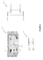
- FIG. 4(a) and 4(b) there are shown two schematic representations 400, 450 of an architecture in accordance with embodiments.
- the conductive lines used to load or readout the state of an electron at a single P atom site 410 are shown.
- the two gate lines 425, 430, the source line 420 and the drain line 415 are biased in a manner to induce an electron to tunnel from a SET island 435 to the corresponding P donor site 410.
- the combination of voltages applied to these control lines is such that an electron can only tunnel through one SET island 435 and no electrons can tunnel through any other SET islands of the matrix of qubits.
- Such configuration of the control lines allows for loading or reading of the state of a single electron on the matrix of qubits.
- the matrix architecture provides the possibility of loading or reading the state of multiple electrons at multiple qubit sites simultaneously, as shown in figure 4(b) .
- multiple conductive lines are controlled to load or readout the state of electrons at a plurality of single P atom sites 460.
- the gate lines 475 and the source lines 470 are activated and biased with appropriate voltages. Electrons can be loaded at any of the donor sites 460 associated with gate lines 475 and source lines 470 by controlling the voltages of the drain lines and gate lines at the upper level of the architecture.
- the drain lines 465 and gate lines 480 are controlled to simultaneously load two electrons on corresponding two P donor sites 460 through the respective SET islands 485.
- the simultaneous control of the different control lines across the matrix allows accessing a plurality of P donor sites at the same time to load electrons or to read the quantum state of the P donor sites.
- This simultaneous, global, control enables rapid operation of the quantum processor.
- the architecture of the apparatus allows simultaneous access to P donor sites arranged in basic patterns, such as lines, rectangles and regular repeating patterns. More complex patterns of sites on the matrix can be realised by iterating combinations of the basic patterns.
- Loading can proceed in several N(load) steps. Each loading step requires a loading time of T(load). In order to preserve the state of the system, for example during the loading phase of the P donor sites 660, the total loading time should be much shorter than the electrons decoherence time: N load T load ⁇ ⁇ T 1 electron
- the electron spins are rotated 430 to be in equal superposition, as discussed above.
- the solution to the problem of interest is encoded in the nuclear or electron spins. Measuring the state of each electron spin 340 may require time. If this time exceeds the typical time during which the electrons are capable of retaining their spin, the accuracy of the solution may be affected.
- FIG. 5 there is shown a flow diagram 500 outlining additional steps used to implement a delayed readout process in accordance with an embodiment.
- a long lived memory function is used during the electrons readout process.
- the memory function is implemented by using the nuclear spin of the phosphorus P donor atoms.
- the steps shown in diagram 500 of Figure 5 are executed after the adiabatic process is completed. If the solution is encoded in the electron spins the state of the electron spin is transferred 505 to the respective nuclear spin state by applying an electromagnetic pulse at a predefined frequency. If the solution is encoded in the state of the nuclear spins step 505 is omitted. The electrons can then be removed 510 from the P donor sites through appropriate biasing of the control lines.
- each spin can be read by loading 520 an electron at a P donor site, transferring 530 the spin state from the nucleus of the P donor to the loaded electron and reading 540 the state of the loaded electron by using the respective conductive lines and SET islands.
- This procedure is applied to every qubit of the matrix until a full readout is obtained.
- the readout procedure described above and illustrated in Figure 5 is a non-destructive procedure and can be repeated many times until the desired readout fidelity is reached.
- the nuclear spin relaxation time is generally much longer than the measurement time and allows for high fidelity reading of thousands of qubits.
- the spins of the free electron of the P donor atoms 110 of the architecture 100 of Figure 1 may interact through exchange interaction or via dipole-dipole interaction.
- the magnitude of each type of interaction varies depending on the physical distance between the P donor atoms 110.
- Figure 6 shows a diagram 600 representing the coupling strengths of electron spins a as a function of the physical separation of the P donor atoms 110.
- the dipole interaction 610 only varies a few orders of magnitude across the whole range of separations in diagram 600.
- the dipole interaction 610 may prevail on the exchange interaction 615, 620, 625 for separations above 20nm depending on the crystal orientation. For separations above 35nm the dipole interaction 610 is larger than the exchange interaction in all three crystal directions.
- the exchange interaction is proportional to the overlap between electronic spin wave functions of the P donor atoms 110 and decays very quickly with the distance between these atoms. This interaction is sensitive to the crystal orientation, due to the different electronic potentials, and varies in strength in one lattice site.
- the exchange interaction may be used in some embodiments where strong coupling of neighbour qubits is required and coupling of higher order neighbours is not crucial, such as in adiabatic quantum computing.
- the dipole interaction although weaker in magnitude, is less variable and can reach higher order neighbour qubits. This interaction may be used in embodiments implementing a gate quantum computer or an adiabatic quantum computer.
- the coupling strength between two qubits on the matrix separated by a distance d is D / d 3 and has a positive sign.
- additional 'coupling qubits' may be added between the 'data qubits'.
- the coupling qubits effectively increase the number of qubits on the qubit matrix. Referring now to figure 7(a) , there is shown an illustration of a two data qubits system 700, with one ancilla qubit 702, positioned between the data qubits 704.
- Figure 7(b) shows the same qubit system 700 where the two data qubits 704 are coupled with an opposite sign to the system 700 of figure 7(a) due to the upwards spin of the ancilla qubit 703.
- the ancilla qubits are loaded at the beginning of the adiabatic protocol, and largely remain in the same state throughout the operation of the adiabatic protocol.
- the coupling between nuclear spins may instead be achieved via the use of coherent electromagnetic pulses, for example ESR pulses.
- ESR pulses coherent electromagnetic pulses
- no electron is loaded onto the ancilla qubit between the two data qubits.
- the data qubits are separated by double the distance, resulting in a dipole coupling which is 8 times weaker than between data qubits and ancilla qubits, and interactions with nuclear spins and an exchange coupling orders of magnitude weaker.
- An alternative coupling method can be implemented by having two ancilla qubits between two data qubits, as illustrated in the system 800 of figure 8.
- Figure 8(a) shows two ancilla qubits 802, positioned between data qubits 804.
- the ancilla qubits 802 are not ionised during the operation of the quantum protocol.
- the ancilla qubits 802 form a spin singlet which provides zero coupling between the data qubits 804.
- the ancilla qubits of system 800 can be initialised in a triplet state, as illustrated in figures 8(b) and 8(c) , to implement spin coupling.
- the ancilla qubits 801 of figure 8(b) form a spin triplet which provides positive coupling between the data qubits 804, whilst the ancilla qubits 803 of figure 8(c) form a spin triplet which provides negative coupling between the data qubits 804.
- a multi-donor quantum dot is placed between the two donors, with the controlled number of electrons loaded onto that dot controlling the coupling.
- the placement of intermediate ancilla qubits with given spins may be used to mediate the coupling between data qubits.
- Figure 9 shows an energy diagram 900 of the ferromagnetic couplings for two donor data qubits with a single intermediate ancilla qubit in between them as the magnetic field is decreased as time progresses.
- the lowest level at time zero is a superposition of the spin states of the two donor qubits, and at time 1.0 the two data qubits are in a ferromagnetic ground state.
- two ancilla qubits are placed between each couple of data qubits to provide an anti-ferromagnetic coupling.
- the two ancilla qubits are placed at a distance of 0.4 d from the respective data qubit, where d is the distance between the data qubits.
- the distance between the two ancilla qubits is 0.2 d .
- qubits couplings are isolated by acting on the nuclear spin and decreasing or eliminating the interaction strength between electrons which occupy sites with different nuclear spin orientations.
- the nuclear spins can be tuned by applying resonant electromagnetic pulses.
- the nuclear spin of the coupling qubit between two data qubits can be targeted regularly to affect the coupling strength.
- each qubit in each chain is coupled to the two neighbouring qubits.
- the qubits disposed about the crossing may interact with each other creating interference.
- the interference due to chain crossing should be decoupled from the qubits interaction.
- chain 920 in figure 10 may be polarised with nuclear spin down and chain 925 with nuclear spin up.
- the interaction strength between electrons occupying sites with different nuclear spin orientations can be reduced by having electrons loaded onto two separate chains, each with a different nuclear spin orientation. In this case the interaction between qubits on the same chain would be promoted whilst the interaction with qubits on the crossing chain would be reduced.
- This may be accomplished by using a pulse sequence which alternately applies pulses to one chain and then the other chain. These pulses have the effect of refocussing inter-chain interactions, but not intra-chain interactions. These pulses must be repeatedly applied during the operation of the quantum computer. These pulses also aid refocusing of any spatially inhomogeneities in the applied direction.
- Errors may be introduced in the quantum computation also by electrons tunnelling between different sites.
- ancilla and data donors may be placed at different potentials. This may be implemented by appropriately biasing the control members placing the data qubits at a different potential to ancilla qubits and suppressing tunnelling between sites, or by using multiple donors at each site with a single electron.
- qubits which are located in different sites of the qubits matrix can be coupled using optical or electrical coupling means realised on the Si substrate 105.
- the optical or electrical coupling means may operate in conjunction with the conductive gates used to address the qubits.
- the control gates may be functionally connected to the optical or electrical means and control the coupling between qubits when addressed with appropriate electronic signals.
- FIG 11 there is shown an alternative architecture for the quantum processor.
- This architecture is an alternative to the architecture of figure 1 .
- the middle layer consists of qubits - separated into data qubits 192 and ancilla qubits 194. Data qubits encode the state of the coupling computer, while ancilla qubits are used to provide couplings between data qubits (as required by the problem Hamiltonian).
- the middle layer also contains the island of vertical SETs placed between source and drain and used both to load electrons onto selected donors, and also to read out nuclear and electron spin states.
- Embodiments of the advanced processing architectures described above may be realised using different semiconductor processing methods.
- the architecture 100 can be realised using scanning tunnelling microscope (STM) micro to atomic-fabrication techniques in conjunction with other fabrication methods common in the microelectronics industry.
- the architecture is realised on a high purity 28 Si substrate with a very low defect concentration and a very high surface quality, likely a floating zone Si substrate.
- the lower source lines 120 and gate lines 125 are realised by introducing a high concentration of dopant atoms, such as P, by STM. By introducing a very high concentration of dopants in some regions of the Si surface, the Si material becomes degeneratively doped and becomes highly conductive.
- the lower layer of the architecture 100 is completed and a first layer of crystalline Si is grown on top of the lower layer by an epitaxy technique, such as molecular beam epitaxy (MBE).
- MBE molecular beam epitaxy
- the thickness of the epitaxial Si layer varies in embodiments of the architecture 100 and defines the spacing between the source and gate electrodes at the lower layer of the architecture and the P donor sites 110 and SET islands 135.
- the P donor sites 110 and SET islands 135 are realised on the surface of the first epitaxial layer.
- the P donor sites 110 are realised by encapsulating a single P atom or cluster of P atoms in the Si surface at each qubit site by STM.
- the SET islands 135 are realised by introducing a very high concentration of dopant atoms in areas of the surface of the first epitaxial layer in the proximity of the P donor sites 110.
- the relative position of each SET island 135 to the respective P donor site 110 affects the biasing configuration of the control lines required to load or readout electrons to and from the P donor site 110.
- a second epitaxial Si layer is grown leading to the upper surface of the architecture 100.
- the drain lines 115 and gate lines 130 may be realised by a STM lithographic doping procedure, or by conventional microelectronics fabrication techniques, such as metal evaporation and/or photolithography.
- the operating temperature of the quantum processor may be below 300 milliKelvin (mK), and may be in the region of 50mK.
- a cooling arrangement may be required to maintain the processing apparatus at this low temperature.
- a source of constant magnetic field and a source of alternating magnetic field may also be required.
- the device also requires means for biasing the control lines by application of voltage.
- adiabatic quantum operation of the advanced processing apparatus has been described.
- the processing apparatus is not limited to this operation.
- a universal quantum processor may be implemented using a similar architecture, and controlling the coupling between qubits so that they are coupled across the apparatus.
- Other advanced processing apparatus may be implemented utilising the architecture of control lines and processing elements.
- an advanced processing apparatus not based on a Si:P system may be implemented.
- control members there are two levels of control members.
- the invention is not limited to this. In other embodiments, there may be more levels of control members, and a corresponding plurality of layers of processing elements forming a "3D" processing apparatus.
- the term 'matrix' has been used to describe qubits arranged in rows and columns, the invention is not limited to that.
- the qubits of the quantum processor may be arranged in different patterns and not be aligned in conventional rows and columns.
Landscapes
- Engineering & Computer Science (AREA)
- Theoretical Computer Science (AREA)
- Physics & Mathematics (AREA)
- General Physics & Mathematics (AREA)
- Software Systems (AREA)
- Mathematical Physics (AREA)
- Artificial Intelligence (AREA)
- Data Mining & Analysis (AREA)
- Evolutionary Computation (AREA)
- Computing Systems (AREA)
- General Engineering & Computer Science (AREA)
- Mathematical Analysis (AREA)
- Computational Mathematics (AREA)
- Condensed Matter Physics & Semiconductors (AREA)
- Mathematical Optimization (AREA)
- Pure & Applied Mathematics (AREA)
- Medical Informatics (AREA)
- Computer Vision & Pattern Recognition (AREA)
- Superconductor Devices And Manufacturing Methods Thereof (AREA)
- Junction Field-Effect Transistors (AREA)
- Bipolar Transistors (AREA)
Applications Claiming Priority (2)
| Application Number | Priority Date | Filing Date | Title |
|---|---|---|---|
| AU2014904417A AU2014904417A0 (en) | 2014-11-03 | Advanced processing apparatus | |
| AU2015900532A AU2015900532A0 (en) | 2015-02-17 | Advanced processing apparatus |
Publications (3)
| Publication Number | Publication Date |
|---|---|
| EP3016035A2 true EP3016035A2 (de) | 2016-05-04 |
| EP3016035A3 EP3016035A3 (de) | 2017-03-08 |
| EP3016035B1 EP3016035B1 (de) | 2019-01-02 |
Family
ID=54427600
Family Applications (2)
| Application Number | Title | Priority Date | Filing Date |
|---|---|---|---|
| EP15192762.1A Active EP3016035B1 (de) | 2014-11-03 | 2015-11-03 | Quantenprozessor |
| EP15192761.3A Active EP3016034B1 (de) | 2014-11-03 | 2015-11-03 | Quantenprozessor |
Family Applications After (1)
| Application Number | Title | Priority Date | Filing Date |
|---|---|---|---|
| EP15192761.3A Active EP3016034B1 (de) | 2014-11-03 | 2015-11-03 | Quantenprozessor |
Country Status (4)
| Country | Link |
|---|---|
| US (2) | US10229365B2 (de) |
| EP (2) | EP3016035B1 (de) |
| AU (2) | AU2015252051B2 (de) |
| ES (1) | ES2787623T3 (de) |
Cited By (5)
| Publication number | Priority date | Publication date | Assignee | Title |
|---|---|---|---|---|
| CN108878519A (zh) * | 2017-05-11 | 2018-11-23 | 原子能和替代能源委员会 | 具有自旋量子位的量子器件 |
| CN113508405A (zh) * | 2019-02-27 | 2021-10-15 | 德国尤里希研究中心 | 用于量子位错误检测的方法和设备 |
| US11687473B2 (en) | 2019-09-20 | 2023-06-27 | Rheinisch-Westfälische Technische Hochschule (Rwth) Aachen | Component for initializing a quantum dot |
| US12133475B2 (en) | 2019-09-20 | 2024-10-29 | Rheinisch-Westfälische Technische Hochschule (Rwth) Aachen | Component having a band assembly for individual electron movement over a long distance |
| WO2026027864A1 (en) * | 2024-07-30 | 2026-02-05 | Riverlane Ltd | A method of performing qubit operations |
Families Citing this family (91)
| Publication number | Priority date | Publication date | Assignee | Title |
|---|---|---|---|---|
| US10068181B1 (en) | 2015-04-27 | 2018-09-04 | Rigetti & Co, Inc. | Microwave integrated quantum circuits with cap wafer and methods for making the same |
| EP3371752B1 (de) * | 2015-11-06 | 2025-04-16 | Google LLC | In-situ-quantenfehlerkorrektur |
| US10352992B1 (en) * | 2016-01-11 | 2019-07-16 | Rigetti & Co, Inc. | Quantum error-correction in microwave integrated quantum circuits |
| EP3300004A1 (de) | 2016-09-27 | 2018-03-28 | Nederlandse Organisatie voor toegepast- natuurwetenschappelijk onderzoek TNO | Verfahren zur ausführung eines quantenfehlerkorrekturzyklus in einem quantencomputer |
| WO2018063269A1 (en) | 2016-09-30 | 2018-04-05 | Intel Corporation | Single electron transistors (sets) and set-based qubit-detector arrangements |
| WO2018143986A1 (en) * | 2017-02-02 | 2018-08-09 | Intel Corporation | Quantum dot array devices |
| US9978020B1 (en) | 2017-03-29 | 2018-05-22 | International Business Machines Corporation | Optimizing physical parameters in fault-tolerant quantum computing to reduce frequency crowding |
| US10141493B2 (en) * | 2017-04-11 | 2018-11-27 | Microsoft Technology Licensing, Llc | Thermal management for superconducting interconnects |
| FI3626034T3 (fi) * | 2017-05-16 | 2026-04-23 | Rigetti & Co Llc | Sähköisen kytkentäjärjestelmän kytkeminen kvanttitietokonejärjestelmässä |
| US11276727B1 (en) | 2017-06-19 | 2022-03-15 | Rigetti & Co, Llc | Superconducting vias for routing electrical signals through substrates and their methods of manufacture |
| US11121301B1 (en) | 2017-06-19 | 2021-09-14 | Rigetti & Co, Inc. | Microwave integrated quantum circuits with cap wafers and their methods of manufacture |
| SG11202001159SA (en) | 2017-07-13 | 2020-03-30 | Harvard College | Neutral atom quantum information processor |
| US10972133B2 (en) * | 2017-08-07 | 2021-04-06 | Microsoft Technology Licensing, Llc | Flag fault-tolerant error correction with arbitrary distance codes |
| US11087233B2 (en) * | 2017-08-09 | 2021-08-10 | Google Llc | Frequency pattern for reducing parasitic interactions in a qubit grid |
| CN111164619B (zh) | 2017-08-09 | 2023-10-31 | 谷歌有限责任公司 | 减少量子比特网格中的寄生相互作用以用于表面代码错误校正 |
| US11694104B2 (en) * | 2017-08-09 | 2023-07-04 | Google Llc | Reducing parasitic interactions in a qubit grid |
| CN111373421B (zh) * | 2017-09-08 | 2023-12-26 | 谷歌有限责任公司 | 具有减少的t门计数的量子电路 |
| EP4216112B1 (de) | 2017-09-13 | 2026-03-11 | Google LLC | Quantenfehlerkorrektur |
| US11281987B2 (en) * | 2017-11-28 | 2022-03-22 | Duke University | Software-defined quantum computer |
| WO2019117955A1 (en) | 2017-12-15 | 2019-06-20 | Klimov Paul | Refining qubit calibration models using supervised learning |
| US11055627B2 (en) | 2018-01-31 | 2021-07-06 | Google Llc | Universal control for implementing quantum gates |
| US10622536B2 (en) | 2018-03-23 | 2020-04-14 | International Business Machines Corporation | Reducing qubit frequency collisions through lattice design |
| CN109583592B (zh) * | 2018-04-25 | 2020-04-17 | 南方科技大学 | 多超导量子比特中任意两个比特耦合的方法及其系统 |
| US11645493B2 (en) | 2018-05-04 | 2023-05-09 | Microsoft Technology Licensing, Llc | Flow for quantized neural networks |
| US11374594B2 (en) * | 2018-05-05 | 2022-06-28 | Intel Corporation | Apparatus and method including neural network learning to detect and correct quantum errors |
| US10453592B1 (en) | 2018-05-07 | 2019-10-22 | Microsoft Technology Licensing Llc | Reducing losses in superconducting cables |
| US11822163B2 (en) | 2018-06-20 | 2023-11-21 | equal1.labs Inc. | Reprogrammable quantum processor architecture |
| US10868119B2 (en) | 2018-06-20 | 2020-12-15 | equal1.labs Inc. | Semiconductor quantum structures using preferential tunneling through thin insulator layers |
| US10854738B2 (en) | 2018-06-20 | 2020-12-01 | equal1.labs Inc. | Semiconductor process for quantum structures with staircase active well |
| US10873019B2 (en) | 2018-06-20 | 2020-12-22 | equal1.labs Inc. | Topological programmable scalable quantum computing machine utilizing chord line quasi unidimensional aperature tunneling semiconductor structures |
| US11450760B2 (en) | 2018-06-20 | 2022-09-20 | equal1.labs Inc. | Quantum structures using aperture channel tunneling through depletion region |
| US10861940B2 (en) | 2018-06-20 | 2020-12-08 | equal1.labs Inc. | Semiconductor process for quantum structures with staircase active well incorporating shared gate control |
| US11423322B2 (en) | 2018-06-20 | 2022-08-23 | equal1.labs Inc. | Integrated quantum computer incorporating quantum core and associated classical control circuitry |
| US10903413B2 (en) | 2018-06-20 | 2021-01-26 | Equal!.Labs Inc. | Semiconductor process optimized for quantum structures |
| US10845496B2 (en) | 2018-06-20 | 2020-11-24 | equal1.labs Inc. | Multistage semiconductor quantum detector circuit incorporating anticorrelation |
| AU2019304104B2 (en) * | 2018-07-20 | 2023-03-09 | Silicon Quantum Computing Pty Limited | A quantum processing system |
| US20210256413A1 (en) * | 2018-08-23 | 2021-08-19 | The University Of Melbourne | Quantum computer arrays |
| EP3844689A4 (de) | 2018-08-30 | 2022-06-08 | Rigetti & Co, LLC | Niedriglatentes, leistungsstarkes hybrid-computing |
| US12165004B2 (en) | 2018-08-31 | 2024-12-10 | President And Fellows Of Harvard College | Quantum computing for combinatorial optimization problems using programmable atom arrays |
| CA3112817A1 (en) | 2018-10-05 | 2020-04-09 | President And Fellows Of Harvard College | Quantum convolutional neural networks |
| US11121302B2 (en) | 2018-10-11 | 2021-09-14 | SeeQC, Inc. | System and method for superconducting multi-chip module |
| US11995512B2 (en) | 2018-11-13 | 2024-05-28 | Atom Computing Inc. | Scalable neutral atom based quantum computing |
| US10504033B1 (en) * | 2018-11-13 | 2019-12-10 | Atom Computing Inc. | Scalable neutral atom based quantum computing |
| US11580435B2 (en) | 2018-11-13 | 2023-02-14 | Atom Computing Inc. | Scalable neutral atom based quantum computing |
| US10333503B1 (en) | 2018-11-26 | 2019-06-25 | Quantum Machines | Quantum controller with modular and dynamic pulse generation and routing |
| US11205030B2 (en) | 2019-01-03 | 2021-12-21 | International Business Machines Corporation | Avoiding data exchange in gate operation for quantum computing gates on a chip |
| US10454459B1 (en) | 2019-01-14 | 2019-10-22 | Quantum Machines | Quantum controller with multiple pulse modes |
| WO2020172588A1 (en) | 2019-02-22 | 2020-08-27 | President And Fellows Of Harvard College | Large-scale uniform optical focus array generation with a phase spatial light modulator |
| WO2020180902A1 (en) * | 2019-03-03 | 2020-09-10 | The University Of Chicago | Technologies for resource-efficient quantum error correction |
| US10505524B1 (en) | 2019-03-06 | 2019-12-10 | Quantum Machines | Synchronization in a quantum controller with modular and dynamic pulse generation and routing |
| US11048839B2 (en) | 2019-03-29 | 2021-06-29 | International Business Machines Corporation | Adaptive error correction in quantum computing |
| US11556411B2 (en) | 2019-04-24 | 2023-01-17 | International Business Machines Corporation | Quantum code for reduced frequency collisions in qubit lattices |
| US11164100B2 (en) | 2019-05-02 | 2021-11-02 | Quantum Machines | Modular and dynamic digital control in a quantum controller |
| CA3138309A1 (en) | 2019-05-17 | 2020-11-26 | President And Fellows Of Harvard College | System and method for multiplexed optical addressing of atomic memories |
| WO2021007560A1 (en) | 2019-07-11 | 2021-01-14 | President And Fellows Of Harvard College | System and method for parallel implementation of multi-qubit quantum gates |
| US10931267B1 (en) | 2019-07-31 | 2021-02-23 | Quantum Machines | Frequency generation in a quantum controller |
| US12579462B1 (en) | 2019-08-14 | 2026-03-17 | Q.M Technologies Ltd. | Controlling a quantum processor via quantum programming field payloads |
| US10862465B1 (en) | 2019-09-02 | 2020-12-08 | Quantum Machines | Quantum controller architecture |
| US11245390B2 (en) | 2019-09-02 | 2022-02-08 | Quantum Machines | Software-defined pulse orchestration platform |
| US12431879B2 (en) | 2019-09-25 | 2025-09-30 | Q.M Technologies Ltd. | Classical processor for quantum control |
| US11763157B2 (en) | 2019-11-03 | 2023-09-19 | Microsoft Technology Licensing, Llc | Protecting deep learned models |
| CA3157734A1 (en) | 2019-11-08 | 2021-05-14 | Peter Carl Hendrickson | System and method using multilayer qubit lattice arrays for quantum computing |
| US12288129B2 (en) * | 2019-11-08 | 2025-04-29 | Kbr Wyle Services, Llc | System and method using multiple entangled linear qubit arrays for quantum computing |
| US11507873B1 (en) | 2019-12-16 | 2022-11-22 | Quantum Machines | Highly scalable quantum control |
| EP3862934A1 (de) * | 2020-02-04 | 2021-08-11 | IQM Finland Oy | Additive steuerung von qubits zur ermöglichung des zeit- und frequenzbereichsmultiplexens |
| US12530222B1 (en) * | 2020-02-10 | 2026-01-20 | Rigetti & Co, Llc | Workload orchestration in hybrid quantum/classical computing systems |
| JP7708774B2 (ja) | 2020-03-02 | 2025-07-15 | アトム コンピューティング インク. | スケーラブルな中性原子ベースの量子コンピューティング |
| KR102887206B1 (ko) | 2020-03-02 | 2025-11-17 | 아톰 컴퓨팅 인크. | 확장 가능한 중성 원자 기반 양자 컴퓨팅 |
| US11126926B1 (en) | 2020-03-09 | 2021-09-21 | Quantum Machines | Concurrent results processing in a quantum control system |
| US11723288B2 (en) * | 2020-03-22 | 2023-08-08 | Fu-Chang Hsu | Quantum bit array |
| US11043939B1 (en) | 2020-08-05 | 2021-06-22 | Quantum Machines | Frequency management for quantum control |
| US12395162B2 (en) | 2020-11-12 | 2025-08-19 | equal1.labs Inc. | System and method of quantum stochastic rounding using silicon based quantum dot arrays |
| EP4305558A4 (de) * | 2021-03-11 | 2025-10-08 | Silicon Quantum Computing Pty Ltd | Quantenverarbeitungselement und quantenverarbeitungssystem |
| JP2024512373A (ja) * | 2021-03-11 | 2024-03-19 | シリコン クワンタム コンピューティング ピーティーワイ リミテッド | キュービットおよび量子処理システム |
| US12132486B2 (en) | 2021-04-08 | 2024-10-29 | Quantum Machines | System and method for pulse generation during quantum operations |
| US11671180B2 (en) | 2021-04-28 | 2023-06-06 | Quantum Machines | System and method for communication between quantum controller modules |
| US12242406B2 (en) | 2021-05-10 | 2025-03-04 | Q.M Technologies Ltd. | System and method for processing between a plurality of quantum controllers |
| US12165011B2 (en) | 2021-06-19 | 2024-12-10 | Q.M Technologies Ltd. | Error detection mechanism for quantum bits |
| US12332682B2 (en) | 2021-07-21 | 2025-06-17 | Q.M Technologies Ltd. | System and method for clock synchronization and time transfer between quantum orchestration platform elements |
| US12602245B2 (en) * | 2021-11-18 | 2026-04-14 | Red Hat, LLC | Quantum isolation zoneslc |
| US12111352B2 (en) | 2022-01-24 | 2024-10-08 | Quantum Machines | Machine learning for syncing multiple FPGA ports in a quantum system |
| WO2024049496A2 (en) * | 2022-01-31 | 2024-03-07 | Streamline Automation Llc | Topological quantum computing systems and methods |
| US12314815B2 (en) | 2022-02-28 | 2025-05-27 | Q.M Technologies Ltd. | Auto-calibrating mixers in a quantum orchestration platform |
| US12493810B2 (en) | 2022-05-09 | 2025-12-09 | Q.M Technologies Ltd. | Pulse generation in a quantum device operator |
| WO2023218310A1 (en) * | 2022-05-09 | 2023-11-16 | 1Qb Information Technologies Inc. | Methods and systems for quantum error correction |
| US12488275B1 (en) | 2022-05-10 | 2025-12-02 | Q.M Technologies Ltd. | Buffering the control of a quantum device |
| EP4526813A4 (de) | 2022-05-19 | 2026-05-06 | Atom Computing Inc | Vorrichtungen und verfahren für hohlraumbasierte berechnung |
| US12450513B2 (en) * | 2022-05-31 | 2025-10-21 | Q.M Technologies Ltd. | Quantum controller validation |
| JP2024018005A (ja) * | 2022-07-28 | 2024-02-08 | 株式会社日立製作所 | 量子情報処理装置及び量子情報処理システム |
| US12549161B2 (en) | 2023-11-29 | 2026-02-10 | Q.M Technologies Ltd. | High resolution, direct synthesis of qubit control signals |
| CN117521831B (zh) * | 2024-01-04 | 2024-03-29 | 合肥微观纪元数字科技有限公司 | 基于图形处理器的量子误差自动化校准方法及相关设备 |
Citations (3)
| Publication number | Priority date | Publication date | Assignee | Title |
|---|---|---|---|---|
| US6369404B1 (en) | 1997-09-17 | 2002-04-09 | Unisearch Limited | Electron devices for single electron and nuclear spin measurement |
| US7547648B2 (en) | 2003-08-20 | 2009-06-16 | Qucor Pty Ltd | Fabricating nanoscale and atomic scale devices |
| US7732804B2 (en) | 2002-08-20 | 2010-06-08 | Quocor Pty. Ltd. | Solid state charge qubit device |
Family Cites Families (6)
| Publication number | Priority date | Publication date | Assignee | Title |
|---|---|---|---|---|
| GB0205011D0 (en) | 2002-03-04 | 2002-04-17 | Univ London | A gate for information processing |
| US7966549B2 (en) * | 2007-03-01 | 2011-06-21 | Qucor Pty. Ltd. | Error corrected quantum computer |
| US9015215B2 (en) | 2008-05-20 | 2015-04-21 | D-Wave Systems, Inc. | Systems, methods, and apparatus for calibrating, controlling, and operating a quantum processor |
| US9256834B2 (en) | 2013-05-29 | 2016-02-09 | Microsoft Technology Licensing, Llc | Quantum computers having partial interferometric quantum gates |
| US9286154B2 (en) * | 2013-06-07 | 2016-03-15 | Alcatel Lucent | Error correction for entangled quantum states |
| US9858531B1 (en) * | 2013-08-02 | 2018-01-02 | University Of Maryland | Fault tolerant scalable modular quantum computer architecture with an enhanced control of multi-mode couplings between trapped ion qubits |
-
2015
- 2015-11-03 US US14/931,768 patent/US10229365B2/en active Active
- 2015-11-03 ES ES15192761T patent/ES2787623T3/es active Active
- 2015-11-03 AU AU2015252051A patent/AU2015252051B2/en active Active
- 2015-11-03 EP EP15192762.1A patent/EP3016035B1/de active Active
- 2015-11-03 AU AU2015252050A patent/AU2015252050B2/en active Active
- 2015-11-03 EP EP15192761.3A patent/EP3016034B1/de active Active
- 2015-11-03 US US14/931,738 patent/US10255556B2/en active Active
Patent Citations (4)
| Publication number | Priority date | Publication date | Assignee | Title |
|---|---|---|---|---|
| US6369404B1 (en) | 1997-09-17 | 2002-04-09 | Unisearch Limited | Electron devices for single electron and nuclear spin measurement |
| US6472681B1 (en) | 1997-09-17 | 2002-10-29 | Unisearch Limited | Quantum computer |
| US7732804B2 (en) | 2002-08-20 | 2010-06-08 | Quocor Pty. Ltd. | Solid state charge qubit device |
| US7547648B2 (en) | 2003-08-20 | 2009-06-16 | Qucor Pty Ltd | Fabricating nanoscale and atomic scale devices |
Cited By (9)
| Publication number | Priority date | Publication date | Assignee | Title |
|---|---|---|---|---|
| CN108878519A (zh) * | 2017-05-11 | 2018-11-23 | 原子能和替代能源委员会 | 具有自旋量子位的量子器件 |
| CN108878519B (zh) * | 2017-05-11 | 2024-02-20 | 原子能和替代能源委员会 | 具有自旋量子位的量子器件 |
| CN113508405A (zh) * | 2019-02-27 | 2021-10-15 | 德国尤里希研究中心 | 用于量子位错误检测的方法和设备 |
| CN113508405B (zh) * | 2019-02-27 | 2024-04-23 | 德国尤里希研究中心 | 用于量子位错误检测的方法和设备 |
| US11687473B2 (en) | 2019-09-20 | 2023-06-27 | Rheinisch-Westfälische Technische Hochschule (Rwth) Aachen | Component for initializing a quantum dot |
| US12072819B2 (en) | 2019-09-20 | 2024-08-27 | Rheinisch-Westfälische Technische Hochschule (Rwth) Aachen | Connection component for branching off a single electron motion |
| US12133475B2 (en) | 2019-09-20 | 2024-10-29 | Rheinisch-Westfälische Technische Hochschule (Rwth) Aachen | Component having a band assembly for individual electron movement over a long distance |
| US12182041B2 (en) | 2019-09-20 | 2024-12-31 | Rheinisch-Westfälische Technische Hochschule (Rwth) Aachen | Manipulation zone for qubits in quantum dots |
| WO2026027864A1 (en) * | 2024-07-30 | 2026-02-05 | Riverlane Ltd | A method of performing qubit operations |
Also Published As
| Publication number | Publication date |
|---|---|
| EP3016035A3 (de) | 2017-03-08 |
| AU2015252050B2 (en) | 2019-08-08 |
| AU2015252051A1 (en) | 2016-05-19 |
| ES2787623T3 (es) | 2020-10-16 |
| EP3016034A2 (de) | 2016-05-04 |
| US20160125311A1 (en) | 2016-05-05 |
| EP3016035B1 (de) | 2019-01-02 |
| AU2015252051B2 (en) | 2020-10-15 |
| AU2015252050A1 (en) | 2016-05-19 |
| EP3016034A3 (de) | 2017-02-22 |
| US10255556B2 (en) | 2019-04-09 |
| US10229365B2 (en) | 2019-03-12 |
| EP3016034B1 (de) | 2020-03-18 |
| US20160125310A1 (en) | 2016-05-05 |
Similar Documents
| Publication | Publication Date | Title |
|---|---|---|
| AU2015252050B2 (en) | A quantum processor | |
| KR100971843B1 (ko) | 자기저항 디바이스 | |
| US9530873B1 (en) | Semiconductor adiabatic qubits | |
| US11610985B2 (en) | Quantum processing system | |
| AU2019326260A1 (en) | "Quantum computer arrays" | |
| US20240290872A1 (en) | Electrical control of a quantum processing element | |
| US20240349626A1 (en) | Advanced quantum processing systems and methods for performing quantum logic operations | |
| US20240169242A1 (en) | Qubit and quantum processing system | |
| Tiwari et al. | Observation of the time-reversal symmetric hall effect in graphene–wse2 heterostructures at room temperature | |
| Jones et al. | Atomic engineering of molecular qubits for high-speed, high-fidelity single qubit gates | |
| AU2019227083B2 (en) | Nuclear spin quantum processing element and method of operation thereof | |
| KR20230155460A (ko) | 양자 처리 요소 및 양자 처리 시스템 | |
| Hayami et al. | Magnetic vortex induced by nonmagnetic impurity in ferromagnets: Magnetic multipole and toroidal around the vacancy | |
| JP4445068B2 (ja) | 量子演算素子および集積回路 | |
| US20260058658A1 (en) | Manipulation of anisotropic g-tensor spin qubits via magnetic field amplification | |
| Sarkar | Spin-orbit coupling mediated electrical control of semiconductor spin qubits: from donor atoms to quantum dots | |
| US20260060006A1 (en) | Tuning spin qubits having anisotropic g-tensors | |
| Abe et al. | Defects for quantum information processing in silicon | |
| FINOCCHIO et al. | Co-Chairs |
Legal Events
| Date | Code | Title | Description |
|---|---|---|---|
| PUAI | Public reference made under article 153(3) epc to a published international application that has entered the european phase |
Free format text: ORIGINAL CODE: 0009012 |
|
| AK | Designated contracting states |
Kind code of ref document: A2 Designated state(s): AL AT BE BG CH CY CZ DE DK EE ES FI FR GB GR HR HU IE IS IT LI LT LU LV MC MK MT NL NO PL PT RO RS SE SI SK SM TR |
|
| AX | Request for extension of the european patent |
Extension state: BA ME |
|
| RAP1 | Party data changed (applicant data changed or rights of an application transferred) |
Owner name: NEWSOUTH INNOVATIONS PTY LIMITED Owner name: UNIVERSITY OF MELBOURNE |
|
| PUAL | Search report despatched |
Free format text: ORIGINAL CODE: 0009013 |
|
| AK | Designated contracting states |
Kind code of ref document: A3 Designated state(s): AL AT BE BG CH CY CZ DE DK EE ES FI FR GB GR HR HU IE IS IT LI LT LU LV MC MK MT NL NO PL PT RO RS SE SI SK SM TR |
|
| AX | Request for extension of the european patent |
Extension state: BA ME |
|
| RIC1 | Information provided on ipc code assigned before grant |
Ipc: G06N 99/00 20100101AFI20170127BHEP |
|
| STAA | Information on the status of an ep patent application or granted ep patent |
Free format text: STATUS: REQUEST FOR EXAMINATION WAS MADE |
|
| 17P | Request for examination filed |
Effective date: 20170829 |
|
| RBV | Designated contracting states (corrected) |
Designated state(s): AL AT BE BG CH CY CZ DE DK EE ES FI FR GB GR HR HU IE IS IT LI LT LU LV MC MK MT NL NO PL PT RO RS SE SI SK SM TR |
|
| GRAP | Despatch of communication of intention to grant a patent |
Free format text: ORIGINAL CODE: EPIDOSNIGR1 |
|
| STAA | Information on the status of an ep patent application or granted ep patent |
Free format text: STATUS: GRANT OF PATENT IS INTENDED |
|
| INTG | Intention to grant announced |
Effective date: 20180711 |
|
| GRAS | Grant fee paid |
Free format text: ORIGINAL CODE: EPIDOSNIGR3 |
|
| GRAA | (expected) grant |
Free format text: ORIGINAL CODE: 0009210 |
|
| STAA | Information on the status of an ep patent application or granted ep patent |
Free format text: STATUS: THE PATENT HAS BEEN GRANTED |
|
| AK | Designated contracting states |
Kind code of ref document: B1 Designated state(s): AL AT BE BG CH CY CZ DE DK EE ES FI FR GB GR HR HU IE IS IT LI LT LU LV MC MK MT NL NO PL PT RO RS SE SI SK SM TR |
|
| REG | Reference to a national code |
Ref country code: GB Ref legal event code: FG4D |
|
| REG | Reference to a national code |
Ref country code: CH Ref legal event code: EP Ref country code: AT Ref legal event code: REF Ref document number: 1085312 Country of ref document: AT Kind code of ref document: T Effective date: 20190115 |
|
| REG | Reference to a national code |
Ref country code: IE Ref legal event code: FG4D |
|
| REG | Reference to a national code |
Ref country code: DE Ref legal event code: R096 Ref document number: 602015022657 Country of ref document: DE |
|
| REG | Reference to a national code |
Ref country code: NL Ref legal event code: FP |
|
| REG | Reference to a national code |
Ref country code: LT Ref legal event code: MG4D |
|
| REG | Reference to a national code |
Ref country code: AT Ref legal event code: MK05 Ref document number: 1085312 Country of ref document: AT Kind code of ref document: T Effective date: 20190102 |
|
| PG25 | Lapsed in a contracting state [announced via postgrant information from national office to epo] |
Ref country code: FI Free format text: LAPSE BECAUSE OF FAILURE TO SUBMIT A TRANSLATION OF THE DESCRIPTION OR TO PAY THE FEE WITHIN THE PRESCRIBED TIME-LIMIT Effective date: 20190102 Ref country code: NO Free format text: LAPSE BECAUSE OF FAILURE TO SUBMIT A TRANSLATION OF THE DESCRIPTION OR TO PAY THE FEE WITHIN THE PRESCRIBED TIME-LIMIT Effective date: 20190402 Ref country code: PL Free format text: LAPSE BECAUSE OF FAILURE TO SUBMIT A TRANSLATION OF THE DESCRIPTION OR TO PAY THE FEE WITHIN THE PRESCRIBED TIME-LIMIT Effective date: 20190102 Ref country code: LT Free format text: LAPSE BECAUSE OF FAILURE TO SUBMIT A TRANSLATION OF THE DESCRIPTION OR TO PAY THE FEE WITHIN THE PRESCRIBED TIME-LIMIT Effective date: 20190102 Ref country code: PT Free format text: LAPSE BECAUSE OF FAILURE TO SUBMIT A TRANSLATION OF THE DESCRIPTION OR TO PAY THE FEE WITHIN THE PRESCRIBED TIME-LIMIT Effective date: 20190502 Ref country code: ES Free format text: LAPSE BECAUSE OF FAILURE TO SUBMIT A TRANSLATION OF THE DESCRIPTION OR TO PAY THE FEE WITHIN THE PRESCRIBED TIME-LIMIT Effective date: 20190102 Ref country code: SE Free format text: LAPSE BECAUSE OF FAILURE TO SUBMIT A TRANSLATION OF THE DESCRIPTION OR TO PAY THE FEE WITHIN THE PRESCRIBED TIME-LIMIT Effective date: 20190102 |
|
| PG25 | Lapsed in a contracting state [announced via postgrant information from national office to epo] |
Ref country code: LV Free format text: LAPSE BECAUSE OF FAILURE TO SUBMIT A TRANSLATION OF THE DESCRIPTION OR TO PAY THE FEE WITHIN THE PRESCRIBED TIME-LIMIT Effective date: 20190102 Ref country code: HR Free format text: LAPSE BECAUSE OF FAILURE TO SUBMIT A TRANSLATION OF THE DESCRIPTION OR TO PAY THE FEE WITHIN THE PRESCRIBED TIME-LIMIT Effective date: 20190102 Ref country code: RS Free format text: LAPSE BECAUSE OF FAILURE TO SUBMIT A TRANSLATION OF THE DESCRIPTION OR TO PAY THE FEE WITHIN THE PRESCRIBED TIME-LIMIT Effective date: 20190102 Ref country code: BG Free format text: LAPSE BECAUSE OF FAILURE TO SUBMIT A TRANSLATION OF THE DESCRIPTION OR TO PAY THE FEE WITHIN THE PRESCRIBED TIME-LIMIT Effective date: 20190402 Ref country code: IS Free format text: LAPSE BECAUSE OF FAILURE TO SUBMIT A TRANSLATION OF THE DESCRIPTION OR TO PAY THE FEE WITHIN THE PRESCRIBED TIME-LIMIT Effective date: 20190502 Ref country code: GR Free format text: LAPSE BECAUSE OF FAILURE TO SUBMIT A TRANSLATION OF THE DESCRIPTION OR TO PAY THE FEE WITHIN THE PRESCRIBED TIME-LIMIT Effective date: 20190403 |
|
| REG | Reference to a national code |
Ref country code: DE Ref legal event code: R097 Ref document number: 602015022657 Country of ref document: DE |
|
| PG25 | Lapsed in a contracting state [announced via postgrant information from national office to epo] |
Ref country code: DK Free format text: LAPSE BECAUSE OF FAILURE TO SUBMIT A TRANSLATION OF THE DESCRIPTION OR TO PAY THE FEE WITHIN THE PRESCRIBED TIME-LIMIT Effective date: 20190102 Ref country code: AL Free format text: LAPSE BECAUSE OF FAILURE TO SUBMIT A TRANSLATION OF THE DESCRIPTION OR TO PAY THE FEE WITHIN THE PRESCRIBED TIME-LIMIT Effective date: 20190102 Ref country code: RO Free format text: LAPSE BECAUSE OF FAILURE TO SUBMIT A TRANSLATION OF THE DESCRIPTION OR TO PAY THE FEE WITHIN THE PRESCRIBED TIME-LIMIT Effective date: 20190102 Ref country code: IT Free format text: LAPSE BECAUSE OF FAILURE TO SUBMIT A TRANSLATION OF THE DESCRIPTION OR TO PAY THE FEE WITHIN THE PRESCRIBED TIME-LIMIT Effective date: 20190102 Ref country code: SK Free format text: LAPSE BECAUSE OF FAILURE TO SUBMIT A TRANSLATION OF THE DESCRIPTION OR TO PAY THE FEE WITHIN THE PRESCRIBED TIME-LIMIT Effective date: 20190102 Ref country code: CZ Free format text: LAPSE BECAUSE OF FAILURE TO SUBMIT A TRANSLATION OF THE DESCRIPTION OR TO PAY THE FEE WITHIN THE PRESCRIBED TIME-LIMIT Effective date: 20190102 Ref country code: EE Free format text: LAPSE BECAUSE OF FAILURE TO SUBMIT A TRANSLATION OF THE DESCRIPTION OR TO PAY THE FEE WITHIN THE PRESCRIBED TIME-LIMIT Effective date: 20190102 Ref country code: AT Free format text: LAPSE BECAUSE OF FAILURE TO SUBMIT A TRANSLATION OF THE DESCRIPTION OR TO PAY THE FEE WITHIN THE PRESCRIBED TIME-LIMIT Effective date: 20190102 |
|
| PLBE | No opposition filed within time limit |
Free format text: ORIGINAL CODE: 0009261 |
|
| STAA | Information on the status of an ep patent application or granted ep patent |
Free format text: STATUS: NO OPPOSITION FILED WITHIN TIME LIMIT |
|
| PG25 | Lapsed in a contracting state [announced via postgrant information from national office to epo] |
Ref country code: SM Free format text: LAPSE BECAUSE OF FAILURE TO SUBMIT A TRANSLATION OF THE DESCRIPTION OR TO PAY THE FEE WITHIN THE PRESCRIBED TIME-LIMIT Effective date: 20190102 |
|
| 26N | No opposition filed |
Effective date: 20191003 |
|
| PG25 | Lapsed in a contracting state [announced via postgrant information from national office to epo] |
Ref country code: SI Free format text: LAPSE BECAUSE OF FAILURE TO SUBMIT A TRANSLATION OF THE DESCRIPTION OR TO PAY THE FEE WITHIN THE PRESCRIBED TIME-LIMIT Effective date: 20190102 |
|
| PG25 | Lapsed in a contracting state [announced via postgrant information from national office to epo] |
Ref country code: TR Free format text: LAPSE BECAUSE OF FAILURE TO SUBMIT A TRANSLATION OF THE DESCRIPTION OR TO PAY THE FEE WITHIN THE PRESCRIBED TIME-LIMIT Effective date: 20190102 |
|
| PG25 | Lapsed in a contracting state [announced via postgrant information from national office to epo] |
Ref country code: MC Free format text: LAPSE BECAUSE OF FAILURE TO SUBMIT A TRANSLATION OF THE DESCRIPTION OR TO PAY THE FEE WITHIN THE PRESCRIBED TIME-LIMIT Effective date: 20190102 Ref country code: LU Free format text: LAPSE BECAUSE OF NON-PAYMENT OF DUE FEES Effective date: 20191103 |
|
| REG | Reference to a national code |
Ref country code: BE Ref legal event code: MM Effective date: 20191130 |
|
| PG25 | Lapsed in a contracting state [announced via postgrant information from national office to epo] |
Ref country code: BE Free format text: LAPSE BECAUSE OF NON-PAYMENT OF DUE FEES Effective date: 20191130 |
|
| PG25 | Lapsed in a contracting state [announced via postgrant information from national office to epo] |
Ref country code: CY Free format text: LAPSE BECAUSE OF FAILURE TO SUBMIT A TRANSLATION OF THE DESCRIPTION OR TO PAY THE FEE WITHIN THE PRESCRIBED TIME-LIMIT Effective date: 20190102 |
|
| PG25 | Lapsed in a contracting state [announced via postgrant information from national office to epo] |
Ref country code: HU Free format text: LAPSE BECAUSE OF FAILURE TO SUBMIT A TRANSLATION OF THE DESCRIPTION OR TO PAY THE FEE WITHIN THE PRESCRIBED TIME-LIMIT; INVALID AB INITIO Effective date: 20151103 Ref country code: MT Free format text: LAPSE BECAUSE OF FAILURE TO SUBMIT A TRANSLATION OF THE DESCRIPTION OR TO PAY THE FEE WITHIN THE PRESCRIBED TIME-LIMIT Effective date: 20190102 |
|
| PG25 | Lapsed in a contracting state [announced via postgrant information from national office to epo] |
Ref country code: MK Free format text: LAPSE BECAUSE OF FAILURE TO SUBMIT A TRANSLATION OF THE DESCRIPTION OR TO PAY THE FEE WITHIN THE PRESCRIBED TIME-LIMIT Effective date: 20190102 |
|
| P01 | Opt-out of the competence of the unified patent court (upc) registered |
Effective date: 20230523 |
|
| PGFP | Annual fee paid to national office [announced via postgrant information from national office to epo] |
Ref country code: NL Payment date: 20251015 Year of fee payment: 11 |
|
| REG | Reference to a national code |
Ref country code: CH Ref legal event code: U11 Free format text: ST27 STATUS EVENT CODE: U-0-0-U10-U11 (AS PROVIDED BY THE NATIONAL OFFICE) Effective date: 20251201 |
|
| PGFP | Annual fee paid to national office [announced via postgrant information from national office to epo] |
Ref country code: DE Payment date: 20251007 Year of fee payment: 11 |
|
| PGFP | Annual fee paid to national office [announced via postgrant information from national office to epo] |
Ref country code: GB Payment date: 20251016 Year of fee payment: 11 |
|
| PGFP | Annual fee paid to national office [announced via postgrant information from national office to epo] |
Ref country code: FR Payment date: 20251008 Year of fee payment: 11 |
|
| PGFP | Annual fee paid to national office [announced via postgrant information from national office to epo] |
Ref country code: CH Payment date: 20251201 Year of fee payment: 11 |
|
| PGFP | Annual fee paid to national office [announced via postgrant information from national office to epo] |
Ref country code: IE Payment date: 20251009 Year of fee payment: 11 |