EP3020068B1 - Elektronisches modul und verfahren zur herstellung davon - Google Patents
Elektronisches modul und verfahren zur herstellung davon Download PDFInfo
- Publication number
- EP3020068B1 EP3020068B1 EP14738461.4A EP14738461A EP3020068B1 EP 3020068 B1 EP3020068 B1 EP 3020068B1 EP 14738461 A EP14738461 A EP 14738461A EP 3020068 B1 EP3020068 B1 EP 3020068B1
- Authority
- EP
- European Patent Office
- Prior art keywords
- metallized layer
- contact pad
- dielectric film
- module
- film
- Prior art date
- Legal status (The legal status is an assumption and is not a legal conclusion. Google has not performed a legal analysis and makes no representation as to the accuracy of the status listed.)
- Active
Links
Images

Classifications
-
- G—PHYSICS
- G06—COMPUTING OR CALCULATING; COUNTING
- G06K—GRAPHICAL DATA READING; PRESENTATION OF DATA; RECORD CARRIERS; HANDLING RECORD CARRIERS
- G06K19/00—Record carriers for use with machines and with at least a part designed to carry digital markings
- G06K19/06—Record carriers for use with machines and with at least a part designed to carry digital markings characterised by the kind of the digital marking, e.g. shape, nature, code
- G06K19/067—Record carriers with conductive marks, printed circuits or semiconductor circuit elements, e.g. credit or identity cards also with resonating or responding marks without active components
- G06K19/07—Record carriers with conductive marks, printed circuits or semiconductor circuit elements, e.g. credit or identity cards also with resonating or responding marks without active components with integrated circuit chips
- G06K19/077—Constructional details, e.g. mounting of circuits in the carrier
- G06K19/07743—External electrical contacts
-
- H—ELECTRICITY
- H10—SEMICONDUCTOR DEVICES; ELECTRIC SOLID-STATE DEVICES NOT OTHERWISE PROVIDED FOR
- H10W—GENERIC PACKAGES, INTERCONNECTIONS, CONNECTORS OR OTHER CONSTRUCTIONAL DETAILS OF DEVICES COVERED BY CLASS H10
- H10W70/00—Package substrates; Interposers; Redistribution layers [RDL]
- H10W70/60—Insulating or insulated package substrates; Interposers; Redistribution layers
- H10W70/699—Insulating or insulated package substrates; Interposers; Redistribution layers for flat cards, e.g. credit cards
-
- H—ELECTRICITY
- H10—SEMICONDUCTOR DEVICES; ELECTRIC SOLID-STATE DEVICES NOT OTHERWISE PROVIDED FOR
- H10W—GENERIC PACKAGES, INTERCONNECTIONS, CONNECTORS OR OTHER CONSTRUCTIONAL DETAILS OF DEVICES COVERED BY CLASS H10
- H10W72/00—Interconnections or connectors in packages
- H10W72/071—Connecting or disconnecting
- H10W72/073—Connecting or disconnecting of die-attach connectors
- H10W72/07331—Connecting techniques
-
- H—ELECTRICITY
- H10—SEMICONDUCTOR DEVICES; ELECTRIC SOLID-STATE DEVICES NOT OTHERWISE PROVIDED FOR
- H10W—GENERIC PACKAGES, INTERCONNECTIONS, CONNECTORS OR OTHER CONSTRUCTIONAL DETAILS OF DEVICES COVERED BY CLASS H10
- H10W74/00—Encapsulations, e.g. protective coatings
- H10W74/10—Encapsulations, e.g. protective coatings characterised by their shape or disposition
- H10W74/15—Encapsulations, e.g. protective coatings characterised by their shape or disposition on active surfaces of flip-chip devices, e.g. underfills
-
- H—ELECTRICITY
- H10—SEMICONDUCTOR DEVICES; ELECTRIC SOLID-STATE DEVICES NOT OTHERWISE PROVIDED FOR
- H10W—GENERIC PACKAGES, INTERCONNECTIONS, CONNECTORS OR OTHER CONSTRUCTIONAL DETAILS OF DEVICES COVERED BY CLASS H10
- H10W90/00—Package configurations
- H10W90/701—Package configurations characterised by the relative positions of pads or connectors relative to package parts
- H10W90/721—Package configurations characterised by the relative positions of pads or connectors relative to package parts of bump connectors
- H10W90/724—Package configurations characterised by the relative positions of pads or connectors relative to package parts of bump connectors between a chip and a stacked insulating package substrate, interposer or RDL
Definitions
- the invention relates to the technical field of electronic modules, to methods of manufacturing electronic modules and modules, as well as to electronic devices, in particular to smart cards, comprising such an electronic module or module. More precisely, the invention relates to electronic modules produced using the so-called “flip chip” technology.
- electronic modules are formed by assembling a dielectric film and a metallized layer.
- the metallized layer comprises contact areas of a connection terminal block, intended to be flush with the surface of an electronic device such as a smart card.
- the chip is fixed to the dielectric film with its active face facing the outside of the film, and its contact pads are connected to the contact pads by means of gold wires which pass through reservations made in the film. thickness of the dielectric film, with regard to the contact pads.
- the chip is then coated in a protective resin.
- FCOS complementary metal-oxide-semiconductor
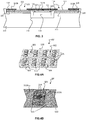
- FIG. 1 represents a schematic sectional view of a module, the chip of which is connected according to the “flip chip” or “flip chip” technique.
- the support film, on which the modules are made is formed by the dielectric film 10 assembled with two metallized layers 20, 30 arranged on each of its faces.
- a first metallized layer 20 is intended to form the module connection terminal block and comprises contact pads such as referenced 21, 22 on the Figure 1 .
- the contact pads are produced, in a known manner, in accordance with the ISO7816-2 standard and are generally 6 or 8.
- the second metallized layer, referenced 30, comprises conductive areas intended to be connected to the contact pads of the first metallized layer 20 by means of conductive wells 11 made in the thickness of the dielectric film in line with the contact pads 21, 22.
- the electronic chip 50 is then transferred so that its active face is placed opposite the zones conductive of the second metallized layer 30 and that its contact pads 51 are electrically connected, via these conductive areas and conductive wells, to the contact pads 21, 22 of the first metallized layer 20.
- a non-conductive adhesive material 52 is generally used to effectively fix the electronic chip on its support.
- Each module, designed on the support film, is then cut and glued in a cavity provided for this purpose in an electronic device, so that the contact pads are flush with the surface of the device.
- This type of electronic module finds application in particular in smart cards.
- the module support film requires in particular two metallized layers on either side of the dielectric film: a first outer layer supporting the contact pads of the connection terminal block in ISO 7816 format and a second inner layer forming conductive areas to allow connection the contact pads of the electronic chip to the contact pads of the first outer layer.
- a module with two metallized layers therefore still remains too expensive.
- the fact of making conductive wells in the dielectric layer is restrictive because the conductive metallized areas and the corresponding conductive wells must then be produced with precision especially for a given chip model.
- the support film does not allow to adapt to any model of chip so that, for each type of chip to be transferred in a module, it is necessary to design a specific support film.
- the design of a module support film, specific for each type of chip, is therefore very restrictive and also involves a high manufacturing cost.
- the DE 39 12 891 A1 discloses an electronic module with the characteristics of the preamble of claim 1, comprising a module support film formed from an assembly of a dielectric film and a metallized layer comprising at least one contact pad of a connection terminal block , said dielectric film forming an external face of said module and comprising at least one opening formed in its thickness and opening onto said at least one contact pad of the metallized layer.
- the EP 0 297 991 A1 discloses an electronic module comprising a module support film formed from an assembly of a dielectric film and a metallized layer comprising at least one contact pad of a connection terminal block, where the contacts accessible through an opening of the card are enhanced by a bump formed under the contacts so that they come approximately at the level of the outer face of the card.
- the DE 10 2009 052 160 A1 shows an electronic module very similar to the module of this Fig. 1 , ie with a second metallized layer comprising conductive zones intended to be connected to the contact pads of the first metallized layer by means of conductive wells formed in the thickness of the dielectric film.
- the aim of the invention is therefore to remedy at least one of the drawbacks of the prior art.
- the invention aims to provide an electronic module that is simple to manufacture, inexpensive, and which can be adapted to any type of electronic chip whatever its size and more generally to any type of electronic component.
- the invention relates to an electronic module comprising a dielectric film and a metallized layer comprising at least one contact pad of a connection terminal block, said dielectric film forming an external face of said module and comprising at least an opening formed in its thickness, said metallized layer being obtained from a metal film, characterized in that a module support film consists of an assembly of said dielectric film and said metallized layer, and in that said at at least one opening opens onto said at least one contact pad of the metallized layer.
- the module only comprises a single metallized layer, which makes it less expensive.
- the metallized layer becomes the support layer of the electronic chip and interconnection tracks can simply and easily be produced, just before the transfer of the chip, depending on its size.
- the module support film, formed by assembling the dielectric film and the metallized layer, can then be adapted to any type of chip.
- the chip can be fixed as a flip-chip (upside down facing towards the rear face of the module or facing away from it).
- the invention also relates to an electronic device comprising at least one electronic module comprising a dielectric film and a metallized layer, provided with at least one contact pad of a connection terminal block accessible from the surface of said device and a chip of which at least one contact pad is electrically connected to said at least one contact pad, characterized in that the dielectric film of said module is flush with the surface of the device, at least one opening, made in the thickness of said film, opening onto said au minus a contact pad to make it accessible.
- the device is a smart card.
- front face In the remainder of the description, the term “front face”, “visible face”, “external face” or “external layer” of an electronic module is understood to mean the face intended to be flush with the surface of an electronic device. On the contrary, the term “rear face” or “hidden face” is understood to mean the face of the module which is intended to be housed in the cavity of an electronic device and to be hidden from the outside.
- metalized layer is used to denote a layer comprising electrically conductive metal zones, for example delimiting contact areas.
- metallic film denotes an entirely metallic layer without delimitation of specific zones.
- the Figure 2 represents an exploded schematic view of an electronic module according to the invention (or at least the module metallization support film in particular for a smart card type device when there is no integrated circuit chip connected).
- This module comprises, on the side of its front face AV, a dielectric film 120.
- This dielectric film 120 can be a portion of an insulating sheet or of an insulating tape. It covers a metallized layer 110 provided with contact pads 111 of a connection terminal block.
- An electronic chip 130 is placed on the rear face AR of the module, and more precisely on the rear face AR of the metallized layer 110, opposite the dielectric film 120.
- the constituent layers of the support film of the module are therefore reversed with respect to a standard support film: the metallized layer becomes the support layer of the electronic compound and the dielectric film forms the outer layer of the module.
- the metallization support films of modules are known by the term "Lead-frame” (conductive metal grid etched and / or transferred to a dielectric film or an insulator).
- openings 121 are made in the thickness of the dielectric film 120, facing each contact area 111 of the metallized layer 110 below.
- the location of the openings 121 therefore complies with the requirements of the ISO7816 standard.
- the size of the openings 121 is at least equal to the size that the contact pads must have according to the ISO 7816-2 standard. It may be slightly greater due to the thickness of the dielectric film.
- the thickness of the dielectric film must also be thin enough so that the arrangement of the contact pads of the module connection terminal block with respect to the surface of an electronic device, in particular of a smart card, complies with the requirements of the ISO7816 standard.
- the thickness of the dielectric film is less than 100 ⁇ m, and preferably between 7 and 50 ⁇ m.
- the dielectric material can advantageously be chosen at least from the following materials: FR4 (from the English acronym Flame Resistant 4) which is a composite material based on epoxy resin reinforced with fiber. glass, PET (polyethylene terephthalate), a polyimide known under the brand name Kapton, PEN (polyethylene naphthalate), PVC (polyvinyl chloride), etc.
- FR4 from the English acronym Flame Resistant 4
- PET polyethylene terephthalate
- PEN polyethylene naphthalate
- PVC polyvinyl chloride
- the metallized layer 110 advantageously comprises two zones.
- a first zone 111 comprises at least one contact pad of a connection terminal block.
- a module connection terminal block comprises 6 or 8 contact pads. These contact pads are made at locations prescribed by the ISO7816 standard, and their size is slightly larger than that prescribed by the ISO7816 standard so that the contact pads are accessible even on the edges of the openings 121 made in the dielectric film.
- a second zone 112A, 112B is provided between the contact pads 111 of this first zone and all around.
- This second zone 112 A, 112B is called a personalization zone. It makes it possible to transfer the electronic chip 130 to it, but also other active and / or passive components. Before the transfer of the chip 130 and any other components, interconnection tracks are made in this customization area in order to be able to electrically connect the contact pads of the chip, and any other components, with certain contact pads 111 of the connection terminal block.
- the support film for the module formed by assembling the dielectric film and the metallized layer, and the customization of the module are produced according to the method described below.
- the openings 121 are made in the dielectric film 120.
- This film is in the form of a strip intended to support modules manufactured continuously along the strip.
- the Figure 4A represents an example of such a film on which are represented 4 modules M1, M2, M3, M4 seen from their front faces.
- the dielectric film 120 provided with its openings 121 is then assembled with the metallized layer 110.
- the metallized layer 110 is produced beforehand according to a conventional method of transferring metal onto a substrate.
- the substrate can for example be an epoxy resin reinforced with glass fibers.
- the conventional process used can for example be a photolithography or electrolytic growth process or else an autocatalytic deposition process.
- This metallized layer comprises the contact pads of the connection terminal block as well as the interconnection tracks intended to connect the contact pads of the chip to be transferred to the contact pads.
- the metallized layer therefore has an architecture dedicated to an electronic component. The metallized layer is then assembled to the dielectric film by lamination, for example.
- the dielectric film 120 is assembled beforehand, by lamination for example, to an entirely metallic film in which the metallized layer is then produced.
- the metallic film is then visible from the front face AV through the openings 121 of the dielectric film 120.
- the contact pads 111, interconnection tracks 114 and component transfer zone are defined, in the metallic film, in a single laser engraving step.
- the rear face AR of the electronic module that is to say the metal film as shown diagrammatically on the Figure 4B , is laser etched in order to draw the outlines of the contact pads 111, and to produce the interconnection tracks 114 according to the chip to be transferred.
- This etching step makes it possible to delimit the contours of the contact pads and of the interconnection tracks and to obtain the metallized layer 110 of the module.
- the interconnection tracks are made according to the chip to be transferred, so that the contact pads of the chip can be connected to corresponding contact pads.
- the metal of the metallic film is removed in component transfer zones, which correspond neither to the contact pads 111 nor to the interconnection tracks 114. It is in fact possible to transfer other passive and / or active components which are then connected to the contact pads of the same way, thanks to interconnection tracks made between the contact pads and the contact pads of the components.
- the dielectric film 120 is assembled beforehand to an entirely metallic film in which the metallized layer is then produced.
- the metal film is laser-etched, so as to remove the metal from the metal film in the personalization zone 112A, 112B and only keep metal to define the contact areas 111 of the connection terminal block. In this case, all the metal around the contour of the contact pads 111 is laser removed. The film is therefore perforated and there is no more metal remaining in the second personalization zone 112A, 112B which is then characterized by the exposed surface of the dielectric film 120. Only the contact pads therefore remain assembled to the dielectric film.
- the interconnection tracks 114 between the contact pads and the contact pads of the electronic chip and / or of the component to be transferred are then designed by applying a conductive material.
- This application is advantageously carried out by inkjet printing.
- the conductive ink used can be chosen from: an ink based on metal nanoparticles, such as nanoparticles of gold, silver, copper or palladium for example, an ink based on carbon nanotubes or graphene , or else an ink based on a conductive polymer, for example.
- the interconnection tracks thus produced and the contact pads then constitute the metallized layer 110 of the module.
- This third embodiment advantageously makes it possible to add passive components, simultaneously with the design of the interconnection tracks, by means of inkjet printing.
- a final step after the design of the interconnection tracks consists of transferring the electronic chip and / or any other active and / or passive component (s).
- the contact pads of the electronic chip are advantageously covered by conductive bosses, commonly called “bumps” or UBM (English acronym for "Under Bump Metalization”) depending on the technology used to make them, referenced 131 on the Figure 3 , which make it possible to ensure electrical continuity between the contact pads of the chip and the interconnection tracks.
- the chip is advantageously arranged so that its active face is facing the metallized layer 110 of the module, and more particularly facing the interconnection tracks 114. It can be transferred either directly to the hidden face of the module, and more particularly on the personalization zone, or be offset and fixed in the cavity of an electronic device, for example.
- FIG. 3 schematically illustrates a sectional view of a chip card portion 200 comprising an electronic module according to the invention, the chip 130 of which is fixed to the hidden face of the module by means of an adhesive referenced 132.
- the chip since the chip is transferred directly from its active face, it is no longer necessary to protect its connections with an encapsulating resin since the connections are already protected by means of the glue. Consequently, the module obtained depends on the thickness of the chip and can therefore be very thin compared to the modules of the prior art.
- the card body 200 advantageously comprises a double cavity 210, 211.
- a first cavity 210 deeper, is intended to house the chip, while the second concentric cavity 211, less deep but of greater length, makes it possible to house the chip.
- the module is fixed to the bottom of the second cavity 211 by means of an adhesive 220, for example a hot-melt adhesive. This adhesive thus makes it possible to directly fix the contact pads of the module and the interconnection tracks in the bottom of the cavity 211.
- the contact pads 111 are accessible from the outside thanks to the openings 121 made in the thickness of the dielectric film. 120 forming the front face of the module.
- the interconnection tracks 114 are advantageously obtained by laser etching 115 of the metal film.
- the support film of the module formed by the assembly of the dielectric film 120 and the metallized layer 110 is transferred and fixed by an adhesive in the cavity 211 of the card body, above the chip. 130 previously fixed by its face opposite to the active face, in the bottom of the cavity 210.
- This module produced in the reverse order of the existing modules until now, offers a great advantage because it adapts to any size of chip, since the interconnection tracks are made just before the transfer of the chip. depending on its size. Furthermore, the large customization zone all around the contact pads offers the possibility of adding other active and / or passive components to create a multi-component module.
- An antenna can also be provided in the personalization zone, by laser engraving of the metal film or by printing by conductive inkjet. The cavity made in the card body is then made as a function of the size of the module.
- the possibility of designing conductive tracks and passive components by printing conductive ink is a very attractive solution in terms of manufacturing cost.
- the support film only comprises a single metallized layer on one side of the dielectric film, which makes it less expensive.
- the module support film is adaptable to any component which also makes it very interesting because it is less expensive to manufacture.
- the manufacture of the module is simple and quick to implement. As a result, the invention makes it possible to manufacture a module which can be adapted to any type of component, in a very simple and inexpensive manner.
Landscapes
- Engineering & Computer Science (AREA)
- Computer Hardware Design (AREA)
- Microelectronics & Electronic Packaging (AREA)
- Physics & Mathematics (AREA)
- General Physics & Mathematics (AREA)
- Theoretical Computer Science (AREA)
- Credit Cards Or The Like (AREA)
Claims (17)
- Elektronisches Modul mit einem dielektrischen Film (120) und einer metallisierten Schicht (110), umfassend mindestens einer Kontaktfläche (111) eines Anschlussklemmenblocks, wobei der dielektrische Film (120) eine Außenseite des Moduls bildet und mindestens eine in ihrer Dicke gebildete Öffnung (121) umfasst, wobei die metallisierte Schicht aus einem Metallfilm erhalten wird, dadurch gekennzeichnet, dass ein Modulträgerfilm aus einer Anordnung des dielektrischen Films (120) und der metallisierten Schicht (110) besteht, und dass die sich mindestens eine Öffnung auf die mindestens eine Kontaktfläche (111) der metallisierten Schicht (110) öffnet.
- Elektronisches Modul nach Anspruch 1, dadurch gekennzeichnet, dass das den dielektrischen Film (120) bildende Material aus mindestens einem der folgenden Materialien ausgewählt ist: glasfaserverstärktes Epoxidharz, Polyethylenterephthalat, Polyimid, Polyethylennaphthalat, Polyvinylchlorid.
- Elektronisches Modul nach einem der Ansprüche 1 oder 2, dadurch gekennzeichnet, dass der dielektrische Film (120) eine Dicke von weniger als 100 µm aufweist.
- Elektronisches Modul nach einem der Ansprüche 1 bis 3, ferner umfassend einen elektronischen Chip (130), der elektrisch mit der mindestens einen Kontaktfläche (111) verbunden ist, dadurch gekennzeichnet, dass er eine verdeckte Seite umfasst, die einen ersten Bereich, der die mindestens eine Kontaktfläche (111) der metallisierten Schicht (110) umfasst, die dazu bestimmt ist, von außen durch die mindestens eine in dem dielektrischen Film (120) eingeführten Öffnung (121) sichtbar zu sein, und einen zweiten Personalisierungsbereich (112A, 112B) umfasst, der dazu bestimmt ist, mindestens eine Verbindungsbahn (114) zum Verbinden mindestens eines der Kontaktpads des Chips mit der mindestens einen Kontaktfläche (111) aufzunehmen.
- Elektronisches Modul nach Anspruch 4, dadurch gekennzeichnet, dass der Personalisierungsbereich Teil der metallisierten Schicht (110) ist.
- Elektronisches Modul nach einem der Ansprüche 4 bis 5, dadurch gekennzeichnet, dass der elektronische Chip (130) in den Personalisierungsbereich übertragen wird, wobei seine aktive Seite der metallisierten Schicht (110) zugewandt ist, wobei mindestens eines seiner Kontaktpads mit der mindestens einen Kontaktfläche (111) über die mindestens eine Verbindungsbahn (114) verbunden ist.
- Elektronisches Modul nach einem der Ansprüche 4 bis 6, dadurch gekennzeichnet, dass es ferner mindestens eine weitere aktive und/oder passive Komponente umfasst, die in dem Personalisierungsbereich angeordnet ist.
- Elektronische Vorrichtung (200) mit mindestens einem elektronischen Modul nach einem der Ansprüche 4 bis 7, wobei die elektronische Vorrichtung dadurch gekennzeichnet ist, dass der dielektrische Film (120) des Moduls bündig mit der Oberfläche der Vorrichtung (200) ist, und dass mindestens eine Öffnung (121), die in der Dicke des dielektrischen Films (120) ausgebildet ist, sich auf die mindestens eine Kontaktfläche (111) öffnet, um sie zugänglich zu machen.
- Elektronische Vorrichtung (200) nach Anspruch 8, dadurch gekennzeichnet, dass die Vorrichtung eine Chipkarte ist.
- Verfahren zur Herstellung eines elektronischen Moduls nach einem der Ansprüche 4 bis 7, wobei das Verfahren dadurch gekennzeichnet ist, dass es die folgenden Schritte umfasst:- Ausführen eines Modulträgerfilms, der aus einer Anordnung des dielektrischen Films (120) und der metallisierten Schicht (110) besteht, wobei der dielektrische Film mindestens eine Öffnung (121) in seiner Dicke umfasst und die metallisierte Schicht mindestens eine der mindestens einen Öffnung (121) zugewandte Kontaktfläche umfasst,- Anordnen des elektronischen Chips (130), wobei die aktive Seite der metallisierten Schicht (110) zugewandt ist, um mindestens eines seiner Kontaktpads mit mindestens einer Kontaktfläche (111) der metallisierten Schicht (110) über mindestens eine Verbindungsbahn (114) zu verbinden.
- Herstellungsverfahren nach Anspruch 10, dadurch gekennzeichnet, dass der Schritt der Ausführung des Modulträgerfilms darin besteht, den dielektrischen Film (120) auf einem Metallfilm anzuordnen und dann die metallisierte Schicht (110) in dem zuvor angeordneten Metallfilm durch Einrichten von mindestens einer Kontaktfläche (111) in dem Metallfilm auszuführen, wobei die Kontaktfläche der mindestens einen Öffnung (121) zugewandt ist, und durch Einrichten mindestens einer Verbindungsbahn (114), die dazu bestimmt ist, mindestens ein Kontaktpad des elektronischen Chips (130) mit der mindestens einen Kontaktfläche (111) zu verbinden.
- Verfahren nach Anspruch 11, dadurch gekennzeichnet, dass die Schritte der Ausführung der mindestens einen Kontaktfläche (111) und der mindestens einen Verbindungsbahn (114) gleichzeitig durch Lasergravur in den Metallfilm ausgeführt werden.
- Herstellungsverfahren nach Anspruch 11, dadurch gekennzeichnet, dass der Schritt der Ausführung der mindestens einen Kontaktfläche (111) durch Lasergravur des Metallfilms ausgeführt wird, wodurch ein Personalisierungsbereich (112A, 112B) auf der Oberfläche des dielektrischen Films (120) auf beiden Seiten der mindestens einen Kontaktfläche (111) erscheint, und dadurch, dass der Schritt der Ausführung der mindestens einen Verbindungsbahn (114) durch Einspritzen von leitfähigem Material in den Personalisierungsbereich erfolgt.
- Herstellungsverfahren nach einem der Ansprüche 10 bis 13, dadurch gekennzeichnet, dass es einen zusätzlichen Schritt umfasst, der darin besteht, mindestens eine andere aktive und/oder passive Komponente auf eine verdeckte Seite des die metallisierte Schicht (110) umfassenden Moduls zu übertragen.
- Herstellungsverfahren nach den Ansprüchen 13 und 14, dadurch gekennzeichnet, dass eine passive Komponente in dem Personalisierungsbereich durch Einspritzen von leitfähigem Material hinzugefügt wird.
- Herstellungsverfahren nach einem der Ansprüche 13 oder 15, dadurch gekennzeichnet, dass das Einspritzen von leitfähigem Material durch Tintenstrahl durchgeführt wird, wobei das leitfähige Material mindestens aus einer Tinte auf Basis von Metallnanopartikeln, einer Tinte auf Basis von Kohlenstoffnanoröhren oder Graphen oder einer Tinte auf Basis eines leitfähigen Polymers ausgewählt ist.
- Verfahren nach einem der Ansprüche 10 bis 16, dadurch gekennzeichnet, dass der elektronische Chip (130) entweder direkt auf die verdeckte Seite des Moduls mit der metallisierten Schicht (110) oder in eine der verdeckten Seite zugewandten Kavität (210) einer elektronischen Vorrichtung gegenüber der verdeckten Fläche übertragen wird.
Applications Claiming Priority (2)
| Application Number | Priority Date | Filing Date | Title |
|---|---|---|---|
| EP20130305996 EP2824704A1 (de) | 2013-07-12 | 2013-07-12 | Elektronisches Modul und sein Herstellungsverfahren |
| PCT/EP2014/064350 WO2015004027A1 (fr) | 2013-07-12 | 2014-07-04 | Module electronique et son procede de fabrication |
Publications (3)
| Publication Number | Publication Date |
|---|---|
| EP3020068A1 EP3020068A1 (de) | 2016-05-18 |
| EP3020068B1 true EP3020068B1 (de) | 2022-01-05 |
| EP3020068B8 EP3020068B8 (de) | 2022-02-16 |
Family
ID=48915950
Family Applications (2)
| Application Number | Title | Priority Date | Filing Date |
|---|---|---|---|
| EP20130305996 Withdrawn EP2824704A1 (de) | 2013-07-12 | 2013-07-12 | Elektronisches Modul und sein Herstellungsverfahren |
| EP14738461.4A Active EP3020068B8 (de) | 2013-07-12 | 2014-07-04 | Elektronisches modul und verfahren zur herstellung davon |
Family Applications Before (1)
| Application Number | Title | Priority Date | Filing Date |
|---|---|---|---|
| EP20130305996 Withdrawn EP2824704A1 (de) | 2013-07-12 | 2013-07-12 | Elektronisches Modul und sein Herstellungsverfahren |
Country Status (3)
| Country | Link |
|---|---|
| EP (2) | EP2824704A1 (de) |
| ES (1) | ES2909790T3 (de) |
| WO (1) | WO2015004027A1 (de) |
Families Citing this family (1)
| Publication number | Priority date | Publication date | Assignee | Title |
|---|---|---|---|---|
| CN106409698A (zh) * | 2016-11-11 | 2017-02-15 | 上海伊诺尔信息技术有限公司 | 智能卡模块的制造方法、智能卡模块及智能卡和条带 |
Family Cites Families (9)
| Publication number | Priority date | Publication date | Assignee | Title |
|---|---|---|---|---|
| FR2486685B1 (fr) * | 1980-07-09 | 1985-10-31 | Labo Electronique Physique | Carte de paiement electronique et procede de realisation |
| DE3123198C2 (de) * | 1980-12-08 | 1993-10-07 | Gao Ges Automation Org | Trägerelemente für einen IC-Baustein |
| FR2505091A1 (fr) * | 1981-04-30 | 1982-11-05 | Cii Honeywell Bull | Dispositif de protection des circuits electroniques tels que des circuits integres a l'encontre des charges electrostatiques |
| FR2581480A1 (fr) * | 1985-04-10 | 1986-11-07 | Ebauches Electroniques Sa | Unite electronique notamment pour carte a microcircuits et carte comprenant une telle unite |
| FR2617666B1 (fr) * | 1987-07-02 | 1989-10-27 | Bull Cp8 | Carte a microcircuits electroniques et son procede de fabrication |
| DE3912891A1 (de) * | 1989-04-19 | 1990-11-08 | Siemens Ag | Montagevorrichtung zur kontaktierung und zum einbau eines integrierten schaltkreissystems fuer eine wertkarte |
| FR2684471B1 (fr) * | 1991-12-02 | 1994-03-04 | Solaic | Procede de fabrication d'une carte a memoire et carte a memoire ainsi obtenue. |
| EP1947691A1 (de) * | 2007-01-18 | 2008-07-23 | Tyco Electronics AMP GmbH | Schaltungsträgerlaminat und Schaltungsträger zur Montage eines Halbleiterchips auf ein Chipkartenmodul sowie Herstellungsverfahren dafür |
| DE102009052160A1 (de) * | 2009-11-06 | 2011-05-12 | Infineon Technologies Ag | Smartcard-Modul mit Flip-Chip montiertem Halbleiterchip |
-
2013
- 2013-07-12 EP EP20130305996 patent/EP2824704A1/de not_active Withdrawn
-
2014
- 2014-07-04 ES ES14738461T patent/ES2909790T3/es active Active
- 2014-07-04 WO PCT/EP2014/064350 patent/WO2015004027A1/fr not_active Ceased
- 2014-07-04 EP EP14738461.4A patent/EP3020068B8/de active Active
Also Published As
| Publication number | Publication date |
|---|---|
| ES2909790T3 (es) | 2022-05-10 |
| EP3020068A1 (de) | 2016-05-18 |
| WO2015004027A1 (fr) | 2015-01-15 |
| EP3020068B8 (de) | 2022-02-16 |
| EP2824704A1 (de) | 2015-01-14 |
Similar Documents
| Publication | Publication Date | Title |
|---|---|---|
| EP3567527B1 (de) | Herstellungsverfahren eines schaltkreises für chipkartenmodul, und schaltkreis für chipkartenmodul | |
| EP3437028B1 (de) | Verfahren zur herstellung von chipkarten und von chipkartenantennenträgern | |
| EP2896067B1 (de) | Kappe für eine chipvorrichtung mit einer nut, vorrichtung mit besagter kappe, baugruppe aus dieser kappe und einem drahtelement sowie herstellungsverfahren dafür | |
| EP2591498A1 (de) | Verfahren zur chipmontage bei einem flexiblen substrat | |
| FR3006551A1 (fr) | Procede de fabrication d'un circuit imprime, circuit imprime obtenu par ce procede et module electronique comportant un tel circuit imprime | |
| EP3408799B1 (de) | Verfahren zur herstellung eines chipkartenmoduls und chipkarte | |
| WO2002009182A1 (fr) | Procede de blindage et/ou de decouplage repartis pour un dispositif electronique a interconnexion en trois dimensions | |
| WO2015101489A9 (fr) | Module electronique, son procede de fabrication, et dispositif electronique comprenant un tel module | |
| FR2937448A1 (fr) | Module, carte a microcircuit et procede de fabrication correspondant. | |
| FR2997550A1 (fr) | Circuit electrique, module electronique pour carte a puce realise sur ce circuit electrique et procede pour la realisation d’un tel circuit electrique. | |
| FR3000604A1 (fr) | Circuit electrique et son procede de realisation | |
| EP2824704A1 (de) | Elektronisches Modul und sein Herstellungsverfahren | |
| EP2866173B1 (de) | Verfahren zur Erzeugung eines elektrischen Schaltkreises, und mit diesem Verfahren erzeugter Schaltkreis | |
| FR2779255A1 (fr) | Procede de fabrication d'un dispositif electronique portable comportant au moins une puce de circuit integre | |
| WO2000077731A1 (fr) | Dispositif et procede de fabrication de dispositifs comprenant au moins une puce montee sur un support | |
| FR2786317A1 (fr) | Procede de fabrication de carte a puce a contact affleurant utilisant une etape de gravure au laser et carte a puce obtenue par le procede | |
| EP3853773A1 (de) | Verfahren zur herstellung eines elektronischen moduls für ein tragbares objekt | |
| WO2015074957A1 (fr) | Procede de fabrication de dispositifs electroniques | |
| FR3006549A1 (fr) | Procede de realisation d'un circuit electrique et circuit electrique realise par ce procede | |
| EP3069304B1 (de) | Vernetzte elektronische vorrichtung und ihr herstellungsverfahren | |
| WO2005064533A1 (fr) | Procedes de fabrication d'une carte du type sans contacts externes, et carte ainsi obtenue | |
| EP1210690B1 (de) | Elektronische vorrichtung mit einer auf einem träger befestigten schaltung, und herstellungsverfahren | |
| WO2002037553A1 (fr) | Connexion de circuit integre par depôt conducteur a travers un film perfore | |
| EP1709574A1 (de) | Verfahren zur herstellung eines elektronischen schlüssels mit usb-verbinder und erhaltener elektronischer schlüssel | |
| FR3127097A1 (fr) | Procédé de fabrication d’un circuit électronique multicouche |
Legal Events
| Date | Code | Title | Description |
|---|---|---|---|
| PUAI | Public reference made under article 153(3) epc to a published international application that has entered the european phase |
Free format text: ORIGINAL CODE: 0009012 |
|
| 17P | Request for examination filed |
Effective date: 20160212 |
|
| AK | Designated contracting states |
Kind code of ref document: A1 Designated state(s): AL AT BE BG CH CY CZ DE DK EE ES FI FR GB GR HR HU IE IS IT LI LT LU LV MC MK MT NL NO PL PT RO RS SE SI SK SM TR |
|
| AX | Request for extension of the european patent |
Extension state: BA ME |
|
| DAX | Request for extension of the european patent (deleted) | ||
| RAP1 | Party data changed (applicant data changed or rights of an application transferred) |
Owner name: THALES DIS FRANCE SA |
|
| STAA | Information on the status of an ep patent application or granted ep patent |
Free format text: STATUS: EXAMINATION IS IN PROGRESS |
|
| 17Q | First examination report despatched |
Effective date: 20191002 |
|
| GRAP | Despatch of communication of intention to grant a patent |
Free format text: ORIGINAL CODE: EPIDOSNIGR1 |
|
| STAA | Information on the status of an ep patent application or granted ep patent |
Free format text: STATUS: GRANT OF PATENT IS INTENDED |
|
| INTG | Intention to grant announced |
Effective date: 20210729 |
|
| GRAS | Grant fee paid |
Free format text: ORIGINAL CODE: EPIDOSNIGR3 |
|
| GRAA | (expected) grant |
Free format text: ORIGINAL CODE: 0009210 |
|
| STAA | Information on the status of an ep patent application or granted ep patent |
Free format text: STATUS: THE PATENT HAS BEEN GRANTED |
|
| AK | Designated contracting states |
Kind code of ref document: B1 Designated state(s): AL AT BE BG CH CY CZ DE DK EE ES FI FR GB GR HR HU IE IS IT LI LT LU LV MC MK MT NL NO PL PT RO RS SE SI SK SM TR |
|
| REG | Reference to a national code |
Ref country code: GB Ref legal event code: FG4D Free format text: NOT ENGLISH |
|
| REG | Reference to a national code |
Ref country code: CH Ref legal event code: EP |
|
| REG | Reference to a national code |
Ref country code: AT Ref legal event code: REF Ref document number: 1461338 Country of ref document: AT Kind code of ref document: T Effective date: 20220115 |
|
| REG | Reference to a national code |
Ref country code: DE Ref legal event code: R081 Ref document number: 602014082019 Country of ref document: DE Owner name: THALES DIS FRANCE SAS, FR Free format text: FORMER OWNER: THALES DIS FRANCE SA, MEUDON, FR |
|
| RAP2 | Party data changed (patent owner data changed or rights of a patent transferred) |
Owner name: THALES DIS FRANCE SAS |
|
| REG | Reference to a national code |
Ref country code: DE Ref legal event code: R096 Ref document number: 602014082019 Country of ref document: DE |
|
| REG | Reference to a national code |
Ref country code: CH Ref legal event code: PK Free format text: RECTIFICATION B8 |
|
| REG | Reference to a national code |
Ref country code: IE Ref legal event code: FG4D Free format text: LANGUAGE OF EP DOCUMENT: FRENCH |
|
| REG | Reference to a national code |
Ref country code: LT Ref legal event code: MG9D |
|
| REG | Reference to a national code |
Ref country code: ES Ref legal event code: FG2A Ref document number: 2909790 Country of ref document: ES Kind code of ref document: T3 Effective date: 20220510 |
|
| REG | Reference to a national code |
Ref country code: NL Ref legal event code: MP Effective date: 20220105 |
|
| REG | Reference to a national code |
Ref country code: AT Ref legal event code: MK05 Ref document number: 1461338 Country of ref document: AT Kind code of ref document: T Effective date: 20220105 |
|
| PG25 | Lapsed in a contracting state [announced via postgrant information from national office to epo] |
Ref country code: NL Free format text: LAPSE BECAUSE OF FAILURE TO SUBMIT A TRANSLATION OF THE DESCRIPTION OR TO PAY THE FEE WITHIN THE PRESCRIBED TIME-LIMIT Effective date: 20220105 |
|
| PG25 | Lapsed in a contracting state [announced via postgrant information from national office to epo] |
Ref country code: SK Free format text: LAPSE BECAUSE OF FAILURE TO SUBMIT A TRANSLATION OF THE DESCRIPTION OR TO PAY THE FEE WITHIN THE PRESCRIBED TIME-LIMIT Effective date: 20220105 Ref country code: SE Free format text: LAPSE BECAUSE OF FAILURE TO SUBMIT A TRANSLATION OF THE DESCRIPTION OR TO PAY THE FEE WITHIN THE PRESCRIBED TIME-LIMIT Effective date: 20220105 Ref country code: RS Free format text: LAPSE BECAUSE OF FAILURE TO SUBMIT A TRANSLATION OF THE DESCRIPTION OR TO PAY THE FEE WITHIN THE PRESCRIBED TIME-LIMIT Effective date: 20220105 Ref country code: PT Free format text: LAPSE BECAUSE OF FAILURE TO SUBMIT A TRANSLATION OF THE DESCRIPTION OR TO PAY THE FEE WITHIN THE PRESCRIBED TIME-LIMIT Effective date: 20220505 Ref country code: NO Free format text: LAPSE BECAUSE OF FAILURE TO SUBMIT A TRANSLATION OF THE DESCRIPTION OR TO PAY THE FEE WITHIN THE PRESCRIBED TIME-LIMIT Effective date: 20220405 Ref country code: LT Free format text: LAPSE BECAUSE OF FAILURE TO SUBMIT A TRANSLATION OF THE DESCRIPTION OR TO PAY THE FEE WITHIN THE PRESCRIBED TIME-LIMIT Effective date: 20220105 Ref country code: HR Free format text: LAPSE BECAUSE OF FAILURE TO SUBMIT A TRANSLATION OF THE DESCRIPTION OR TO PAY THE FEE WITHIN THE PRESCRIBED TIME-LIMIT Effective date: 20220105 Ref country code: BG Free format text: LAPSE BECAUSE OF FAILURE TO SUBMIT A TRANSLATION OF THE DESCRIPTION OR TO PAY THE FEE WITHIN THE PRESCRIBED TIME-LIMIT Effective date: 20220405 |
|
| PG25 | Lapsed in a contracting state [announced via postgrant information from national office to epo] |
Ref country code: PL Free format text: LAPSE BECAUSE OF FAILURE TO SUBMIT A TRANSLATION OF THE DESCRIPTION OR TO PAY THE FEE WITHIN THE PRESCRIBED TIME-LIMIT Effective date: 20220105 Ref country code: LV Free format text: LAPSE BECAUSE OF FAILURE TO SUBMIT A TRANSLATION OF THE DESCRIPTION OR TO PAY THE FEE WITHIN THE PRESCRIBED TIME-LIMIT Effective date: 20220105 Ref country code: GR Free format text: LAPSE BECAUSE OF FAILURE TO SUBMIT A TRANSLATION OF THE DESCRIPTION OR TO PAY THE FEE WITHIN THE PRESCRIBED TIME-LIMIT Effective date: 20220406 Ref country code: FI Free format text: LAPSE BECAUSE OF FAILURE TO SUBMIT A TRANSLATION OF THE DESCRIPTION OR TO PAY THE FEE WITHIN THE PRESCRIBED TIME-LIMIT Effective date: 20220105 Ref country code: AT Free format text: LAPSE BECAUSE OF FAILURE TO SUBMIT A TRANSLATION OF THE DESCRIPTION OR TO PAY THE FEE WITHIN THE PRESCRIBED TIME-LIMIT Effective date: 20220105 |
|
| PG25 | Lapsed in a contracting state [announced via postgrant information from national office to epo] |
Ref country code: IS Free format text: LAPSE BECAUSE OF FAILURE TO SUBMIT A TRANSLATION OF THE DESCRIPTION OR TO PAY THE FEE WITHIN THE PRESCRIBED TIME-LIMIT Effective date: 20220505 |
|
| REG | Reference to a national code |
Ref country code: DE Ref legal event code: R097 Ref document number: 602014082019 Country of ref document: DE |
|
| PG25 | Lapsed in a contracting state [announced via postgrant information from national office to epo] |
Ref country code: SM Free format text: LAPSE BECAUSE OF FAILURE TO SUBMIT A TRANSLATION OF THE DESCRIPTION OR TO PAY THE FEE WITHIN THE PRESCRIBED TIME-LIMIT Effective date: 20220105 Ref country code: RO Free format text: LAPSE BECAUSE OF FAILURE TO SUBMIT A TRANSLATION OF THE DESCRIPTION OR TO PAY THE FEE WITHIN THE PRESCRIBED TIME-LIMIT Effective date: 20220105 Ref country code: EE Free format text: LAPSE BECAUSE OF FAILURE TO SUBMIT A TRANSLATION OF THE DESCRIPTION OR TO PAY THE FEE WITHIN THE PRESCRIBED TIME-LIMIT Effective date: 20220105 Ref country code: DK Free format text: LAPSE BECAUSE OF FAILURE TO SUBMIT A TRANSLATION OF THE DESCRIPTION OR TO PAY THE FEE WITHIN THE PRESCRIBED TIME-LIMIT Effective date: 20220105 Ref country code: CZ Free format text: LAPSE BECAUSE OF FAILURE TO SUBMIT A TRANSLATION OF THE DESCRIPTION OR TO PAY THE FEE WITHIN THE PRESCRIBED TIME-LIMIT Effective date: 20220105 |
|
| PLBE | No opposition filed within time limit |
Free format text: ORIGINAL CODE: 0009261 |
|
| STAA | Information on the status of an ep patent application or granted ep patent |
Free format text: STATUS: NO OPPOSITION FILED WITHIN TIME LIMIT |
|
| PG25 | Lapsed in a contracting state [announced via postgrant information from national office to epo] |
Ref country code: AL Free format text: LAPSE BECAUSE OF FAILURE TO SUBMIT A TRANSLATION OF THE DESCRIPTION OR TO PAY THE FEE WITHIN THE PRESCRIBED TIME-LIMIT Effective date: 20220105 |
|
| 26N | No opposition filed |
Effective date: 20221006 |
|
| PG25 | Lapsed in a contracting state [announced via postgrant information from national office to epo] |
Ref country code: SI Free format text: LAPSE BECAUSE OF FAILURE TO SUBMIT A TRANSLATION OF THE DESCRIPTION OR TO PAY THE FEE WITHIN THE PRESCRIBED TIME-LIMIT Effective date: 20220105 Ref country code: MC Free format text: LAPSE BECAUSE OF FAILURE TO SUBMIT A TRANSLATION OF THE DESCRIPTION OR TO PAY THE FEE WITHIN THE PRESCRIBED TIME-LIMIT Effective date: 20220105 |
|
| REG | Reference to a national code |
Ref country code: CH Ref legal event code: PL |
|
| REG | Reference to a national code |
Ref country code: BE Ref legal event code: MM Effective date: 20220731 |
|
| PG25 | Lapsed in a contracting state [announced via postgrant information from national office to epo] |
Ref country code: LU Free format text: LAPSE BECAUSE OF NON-PAYMENT OF DUE FEES Effective date: 20220704 Ref country code: LI Free format text: LAPSE BECAUSE OF NON-PAYMENT OF DUE FEES Effective date: 20220731 Ref country code: CH Free format text: LAPSE BECAUSE OF NON-PAYMENT OF DUE FEES Effective date: 20220731 |
|
| PG25 | Lapsed in a contracting state [announced via postgrant information from national office to epo] |
Ref country code: BE Free format text: LAPSE BECAUSE OF NON-PAYMENT OF DUE FEES Effective date: 20220731 |
|
| P01 | Opt-out of the competence of the unified patent court (upc) registered |
Effective date: 20230517 |
|
| PG25 | Lapsed in a contracting state [announced via postgrant information from national office to epo] |
Ref country code: IE Free format text: LAPSE BECAUSE OF NON-PAYMENT OF DUE FEES Effective date: 20220704 |
|
| PG25 | Lapsed in a contracting state [announced via postgrant information from national office to epo] |
Ref country code: HU Free format text: LAPSE BECAUSE OF FAILURE TO SUBMIT A TRANSLATION OF THE DESCRIPTION OR TO PAY THE FEE WITHIN THE PRESCRIBED TIME-LIMIT; INVALID AB INITIO Effective date: 20140704 |
|
| PG25 | Lapsed in a contracting state [announced via postgrant information from national office to epo] |
Ref country code: MK Free format text: LAPSE BECAUSE OF FAILURE TO SUBMIT A TRANSLATION OF THE DESCRIPTION OR TO PAY THE FEE WITHIN THE PRESCRIBED TIME-LIMIT Effective date: 20220105 Ref country code: CY Free format text: LAPSE BECAUSE OF FAILURE TO SUBMIT A TRANSLATION OF THE DESCRIPTION OR TO PAY THE FEE WITHIN THE PRESCRIBED TIME-LIMIT Effective date: 20220105 |
|
| PG25 | Lapsed in a contracting state [announced via postgrant information from national office to epo] |
Ref country code: MT Free format text: LAPSE BECAUSE OF FAILURE TO SUBMIT A TRANSLATION OF THE DESCRIPTION OR TO PAY THE FEE WITHIN THE PRESCRIBED TIME-LIMIT Effective date: 20220105 |
|
| PGFP | Annual fee paid to national office [announced via postgrant information from national office to epo] |
Ref country code: ES Payment date: 20250801 Year of fee payment: 12 |
|
| PGFP | Annual fee paid to national office [announced via postgrant information from national office to epo] |
Ref country code: DE Payment date: 20250620 Year of fee payment: 12 |
|
| REG | Reference to a national code |
Ref country code: DE Ref legal event code: R079 Ref document number: 602014082019 Country of ref document: DE Free format text: PREVIOUS MAIN CLASS: H01L0023498000 Ipc: H10W0070620000 |
|
| PG25 | Lapsed in a contracting state [announced via postgrant information from national office to epo] |
Ref country code: TR Free format text: LAPSE BECAUSE OF FAILURE TO SUBMIT A TRANSLATION OF THE DESCRIPTION OR TO PAY THE FEE WITHIN THE PRESCRIBED TIME-LIMIT Effective date: 20220105 |
|
| PGFP | Annual fee paid to national office [announced via postgrant information from national office to epo] |
Ref country code: GB Payment date: 20260618 Year of fee payment: 13 |
|
| PGFP | Annual fee paid to national office [announced via postgrant information from national office to epo] |
Ref country code: IT Payment date: 20260618 Year of fee payment: 13 |
|
| PGFP | Annual fee paid to national office [announced via postgrant information from national office to epo] |
Ref country code: FR Payment date: 20260619 Year of fee payment: 13 |