EP3021090B1 - Kontrollsystem mit e/a-modul - Google Patents
Kontrollsystem mit e/a-modul Download PDFInfo
- Publication number
- EP3021090B1 EP3021090B1 EP15193828.9A EP15193828A EP3021090B1 EP 3021090 B1 EP3021090 B1 EP 3021090B1 EP 15193828 A EP15193828 A EP 15193828A EP 3021090 B1 EP3021090 B1 EP 3021090B1
- Authority
- EP
- European Patent Office
- Prior art keywords
- output
- input
- signal
- controller
- field device
- Prior art date
- Legal status (The legal status is an assumption and is not a legal conclusion. Google has not performed a legal analysis and makes no representation as to the accuracy of the status listed.)
- Active
Links
Images

Classifications
-
- H—ELECTRICITY
- H03—ELECTRONIC CIRCUITRY
- H03K—PULSE TECHNIQUE
- H03K9/00—Demodulating pulses which have been modulated with a continuously-variable signal
- H03K9/08—Demodulating pulses which have been modulated with a continuously-variable signal of duration- or width-mudulated pulses or of duty-cycle modulated pulses
-
- G—PHYSICS
- G05—CONTROLLING; REGULATING
- G05B—CONTROL OR REGULATING SYSTEMS IN GENERAL; FUNCTIONAL ELEMENTS OF SUCH SYSTEMS; MONITORING OR TESTING ARRANGEMENTS FOR SUCH SYSTEMS OR ELEMENTS
- G05B19/00—Program-control systems
- G05B19/02—Program-control systems electric
- G05B19/04—Program control other than numerical control, i.e. in sequence controllers or logic controllers
- G05B19/042—Program control other than numerical control, i.e. in sequence controllers or logic controllers using digital processors
- G05B19/0423—Input/output
Definitions
- the present disclosure related to an input/output (I/O) module, and more specifically, to the I/O module configured to connect a controller, which configures a variety of control systems of a power plant, a manufacturing process, water and sewerage, urban gas and the like, and a field device provided at an outside of the control system.
- a controller which configures a variety of control systems of a power plant, a manufacturing process, water and sewerage, urban gas and the like, and a field device provided at an outside of the control system.
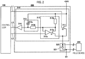
- Fig. 2 is a block diagram for one channel, which depicts a connection example of a field device in a control system of the related art.
- a controller 100 and a field device 200 are connected via an interface circuit 300.
- the interface circuit 300 has a signal unit 310 and an output unit 320.
- the signal unit 310 has a FET (field effect transistor) 311 functioning as a switching element, a current source 312, a filter 313, and a buffer amplifier 314.
- FET field effect transistor
- a source of the FET 311 is connected to a direct current power supply line of +24V, one end of a resistance 312b configuring the current source 312 and one end of a capacitor 313a configuring the filter 313.
- a gate of the FET 311 is connected to the controller 100.
- a drain of the FET 311 is connected to a cathode of a clamp diode 321 configuring the output unit 320 and a drain of a FET 312a configuring the current source 312.
- the current source 312 has the FET 312a, the resistance 312b and an operational amplifier 312c.
- a source of the FET 312a is directly connected to one input terminal of the operational amplifier 312c and one end of a resistance 313b configuring the filter 313 and is also connected to the source of the FET 311 and the one end of the capacitor 313a configuring the filter 313 via the resistance 312b.
- a drain of the FET 312a is connected to the cathode of the clamp diode 321 configuring the output unit 320 and the drain of the FET 311.
- a gate of the FET 312a is connected to an output terminal of the operational amplifier 312c.
- the other input terminal of the operational amplifier 312c is connected to the controller 100.
- the filter 313 has the capacitor 313a and the resistance 313b.
- a connection point of the capacitor 313a and the resistance 313b configuring the filter 313 is connected to the controller 100 via the buffer amplifier 314.
- the output unit 320 has the clamp diode 321.
- An anode of the clamp diode 321 is connected to a direct current power supply line of 0V, and the cathode is connected to the drain of the FET 311 and the drain of the FET 312a. Both ends of the clamp diode 321 are connected with the field device 200.
- the controller 100 and the interface circuit 300 are configured to operate in conjunction with each other so that the connection line L1 is involved at a digital output (DO) mode, the connection line L2 is involved at an analog output (AO) mode, and the connection line L3 is involved at an analog input (AI) mode and a digital input (DI) mode, for example.
- DO digital output
- AO analog output
- DI digital input
- the current source 312 is used at the analog output (AO) mode, and the FET 311 functioning as the switching element is used at the digital output (DO) mode.
- Patent Document 1 discloses the circuit configuration shown in Fig. 2 and operations thereof.
- Patent Document 1 U.S. Patent No. 8,392,626B
- a signal line, which is configured to transmit a control signal, of the signal lines configured to electrically connect the controller 100 and the interface circuit 300 includes an analog signal, and a signal for each function mode is provided. Therefore, the cost of the controller 100 increases and a mount area of a circuit component increases.
- the current source 312 that is to be used at the analog output (AO) mode should be provided with an operational amplifier for each channel so as to keep the output precision of each channel, which also increases the cost and the mount area.
- a size of the interface circuit 300 also increases, so that the power consumption and the heat generation also increase and the system is enlarged.
- US 2013/163688 A1 discloses a control apparatus and methods transferring information between devices, such as controllers and field devices, utilizing a modulator that generates a pulse width modulated (PWM) signal containing information to be transferred by a first of the devices, e.g. the controller, to the second device.
- a transformer or another inductive device transfers the PWM signal across the isolation barrier, where it is demodulated to analog form for application to the second device, e.g. the field device.
- Information transferred from the second device to the first device can be transferred in an amplitude modulated (AM) signal that utilizes, as its carrier, a fixed duty cycle output of the modulator that generates the PWM signal.
- AM amplitude modulated
- DE 10 2008 054053 A1 discloses a field device for process automation, wherein the field device comprises a signal processing unit that generates a digital measurement, control or regulation signal, and comprises an output stage that converts the digital measurement, control or regulation signal into an analog voltage or current signal.
- an output module slice for controlling an output current comprising: an output field interface controller for controlling an input voltage to a first field effect transistor; an analogue to digital converter connected to read the current flowing through said first field effect transistor and to provide a digital signal dependent thereon to said output field interface controller.
- Exemplary embodiments of the invention provide an I/O module capable of miniaturizing a control system and saving the cost thereof without adversely affecting the output precision and the like.
- control system comprising an I/O module as set out in independent claim 1.
- Fig. 1 depicts a configuration of an exemplary embodiment of an input/output (I/O) module of the present invention.
- I/O input/output
- a common controller 10 and field devices 20 of a plurality of n systems are connected to each other via I/O modules 30, respectively.
- the current that is output from each I/O module 30 to each field device 20 is feedback input to the controller 10 via a signal conversion unit 40.
- the controller 10 has a measuring unit 11, a multiplexer 12, a plurality of n measuring systems, an arithmetic controller 16, and the like.
- the multiplexer 12 is configured to selectively output a measured value of the measuring unit 11 to the predetermined corresponding measuring system.
- Each measuring system has a subtractor 13, an integrator 14 and a pulse width modulator (hereinafter, referred to as PWM modulator) 15.
- PWM modulator pulse width modulator
- the arithmetic controller 16 is commonly connected to the plurality of n measuring systems via a control bus B.
- the controller 10 When one of an analog output (AO) mode in which an analog output is performed with respect to the field device 20, a digital output (DO) mode in which a digital output is performed with respect to the field device 20, an analog input (AI) mode in which an analog input is performed from the field device 20, and a digital input (DI) mode in which a digital input is performed from the field device 20 is selected, the controller 10 outputs a PWM signal corresponding to the selected mode. In the meantime, the arithmetic controller 16 is connected with an external controller (not shown).
- one input terminal of the subtractor 13 is input with a measured value (for example, 16 bits) of each measuring system via the multiplexer 12, and the other input terminal is input with a setting value (for example, 16 bits) of each measuring system via the arithmetic controller 16 and the control bus B.
- the subtractor 13 of each measuring system is configured to sequentially output a difference value between the measured value and the setting value to the integrator 14.
- An output value of the integrator 14 of each measuring system converges on a predetermined value associated with the setting value that is individually set for each measuring system.
- the controller 10 may be configured by an FPGA (Field Programmable Gate Array), for example.
- FPGA Field Programmable Gate Array
- the I/O module 30 has a PWM demodulator 31, a current source 32, and an output unit 33.
- the PWM demodulator 31 has a FET 31a, a parallel circuit of a capacitor 31b and a resistance 31c of which one ends are respectively connected to a drain of the FET 31a and the other ends are respectively connected to a power supply line V+, and a resistance 31d of which one end is connected to a source of the FET 31a and the other end is connected to a common potential point.
- a gate of the FET 31a is connected with an output terminal of the PWM modulator 15 of a predetermined measuring system.
- the current source 32 has a FET 32a, and a resistance 32b of which one end is connected to a source of the FET 32a and the other end is connected to the power supply line V+.
- a gate of the FET 32a is connected to the drain of the FET 31a, and a drain of the FET 32a is connected to one end of a resistance 33a configuring the output unit 33.
- the output unit 33 has the resistance 33a of which one end is connected to the drain of the FET 32a and the other end is connected to an anode of a diode 33b, and the diode 33b of which the anode is connected to the other end of the resistance 33a and a cathode is connected to the field device 20.
- the resistance 33a of the output unit 33 is configured to function as a reference resistance for setting a threshold level at a digital input (DI) mode, and is also configured to function as a resistance for current measurement at an analog input (AI) mode.
- DI digital input
- AI analog input
- the diode 33b of the output unit 33 functions to automatically switch the connection when the I/O module 30 and the field device 20 are duplicated.
- the diode 33b of the output unit 33 is connected with the field device 20.
- the signal conversion unit 40 has a multiplexer 41 configured to selectively output a voltage of the resistance 33a of the output unit 33 configuring the I/O module 30 in each measuring system, a differential amplifier 42 connected to an output terminal of the multiplexer 41, and an A/D converter 43 connected to an output terminal of the differential amplifier 42 and configured to convert an output of the differential amplifier into a digital signal.
- the output current that is supplied from the current source 32 to the field device 20 by controlling the PWM signal is converted into the voltage by the resistance 33a configuring the output unit 33, which is then converted into a digital signal, like the analog input (AI) mode.
- the digital signal is compared as the measured value with the setting value and the feedback operation is repeated, so that the output current is controlled to be the same as the setting value all the time.
- the converted digital signal is used for monitoring the analog output value.
- the setting value n that is set by the controller 10 is set for each measuring system through the arithmetic controller 16.
- the digital signal converted by the A/D converter 43 of the signal conversion unit 40 becomes a digital signal as the measured value n of each measuring system through the measuring unit 11 and the multiplexer 12.
- the setting value n and the measured value n are input to the subtractor 13, and the subtractor 13 calculates and outputs a difference thereof.
- the output digital signal is input and periodically integrated in the integrator 14.
- An output of the integrator 14 is converted into a PWM waveform at the PWM modulator 15, and the PWM waveform output is input to the PWM demodulator 31 of the I/O module 30 in each measuring system.
- the series of controls are repeatedly performed, so that the measured value of each measuring system at a normal state substantially coincides with the setting value, the output of the integrator 14 is a substantially constant value and the PWM modulation output of the PWM modulator 15 also converges on a substantially constant pulse width.
- each measuring system can be feedback controlled every 16 seconds.
- the feedback period of each channel being used is 8 seconds, so that it is possible to implement the high speed.
- the precision of the circuit configuration based on the disclosure depends on the resistance 33a of the output unit 33 and the reference voltage precision of the A/D converter 43.
- the resistance 33a of the output unit 33 is configured to be replaceable from an outside, it is possible to easily change a measuring range for each measuring system.
- the output current is monitored and adjusted for each measuring system. Therefore, the parallel operation can be performed with being connected to the output terminals of the plurality of measuring systems.
- the feedback is not an analog feedback by the operational amplifier and the like, it is possible to detect a contact failure of the wiring, an access of a noise source and the like on the basis of the voltage drop of the resistance 33a of the output unit 33 at the digital input (DI) mode and the digital output (DO) mode.
- circuit configuration of the embodiment it is possible to reduce the circuit size with keeping the high precision without providing the operational amplifier for each measuring system, to suppress the heat generation, to save the cost and the reduce the failure occurrence.
- the signal conversion unit 40 is provided with the multiplexer 41, so that it is possible to commonly use the differential amplifier 42 and the A/D converter 43 in the plurality of measuring systems.
- the multichannel (for example, 16 channels) of the measuring systems it is possible to remarkably reduce the circuit space and the overall cost.
Landscapes
- Physics & Mathematics (AREA)
- General Physics & Mathematics (AREA)
- Engineering & Computer Science (AREA)
- Automation & Control Theory (AREA)
- Arrangements For Transmission Of Measured Signals (AREA)
- Programmable Controllers (AREA)
- Analogue/Digital Conversion (AREA)
Claims (5)
- Ein Steuerungssystem, das ein Eingangs-/Ausgangs-(E/A)-Modul (30) und eine Steuerung (10) aufweist, wobei die Steuerung (10) über das Eingangs-/Ausgangs-(E/A)-Modul mit einem Feldgerät (20) verbunden werden kann, wobei das E/A-Modul (30) aufweist:einen PWM (Pulsweitenmodulation)-Demodulator (31), der konfiguriert ist, um ein PWM-Signal zu demodulieren, das von der Steuerung (10) eingegeben wird;eine Stromquelle (32), die konfiguriert ist, um einen Strom basierend auf einem Ausgangssignal des PWM-Demodulators (31) an das Feldgerät (20) auszugeben;einen Widerstand (33a), der in Reihe mit der Stromquelle (32) geschaltet ist; undeine Signalumwandlungseinheit (40), die konfiguriert ist, um einen Ausgangsstrom der Stromquelle (32) über die Steuerung (10) an den PWM-Demodulator (31) zurückzuführen,wobei die Signalumwandlungseinheit (40) einen A/D-Wandler (43) aufweist, der konfiguriert ist, um ein analoges Signal in ein digitales Signal umzuwandeln, und ein Strom eines analogen Eingangs, der über den Widerstand (33a) erfasst wird, über den A/D-Wandler (43) in die Steuerung (10) eingegeben wird,wobei das Steuerungssystem dadurch gekennzeichnet ist, dassdie Steuerung angepasst ist, um ein jeweiliges PWM-Signal entsprechend einem jeweiligen von Modi auszugeben, die einen analogen Ausgabemodus, in dem ein Strom eines Einstellwerts veranlasst wird, von der Stromquelle (32) über einen Widerstand (33a) an das Feldgerät (20) ausgegeben zu werden, und ein analoges Signal somit an das Feldgerät (20) ausgegeben wird, einen digitalen Ausgabemodus, in dem ein Strom, der dem Ein- und Ausschalten eines digitalen Ausgabewerts entspricht, veranlasst wird, von der Stromquelle (32) über einen Widerstand (33a) an das Feldgerät (20) ausgegeben zu werden, und ein digitales Signal somit an das Feldgerät (20) ausgegeben wird, einen analogen Eingabemodus, in dem bewirkt wird, dass eine Stromversorgungsspannung an dem Feldgerät von der Stromquelle (32) über einen Widerstand (33a) zugeführt wird, und ein analoges Signal von dem Feldgerät (20) eingegeben wird, und einen digitalen Eingabemodus umfasst, in dem bewirkt wird, dass eine Stromversorgungsspannung an dem Feldgerät von der Stromquelle (32) über einen Widerstand (33a) zugeführt wird und ein digitales Signal von dem Feldgerät (20) eingegeben wird, undwobei in dem analogen Eingabemodus das umgewandelte digitale Signal des A/D-Wandlers (43) in die Steuerung (10) als ein analoger Eingabemesswert eingegeben wird, und wobei in dem digitalen Eingabemodus das umgewandelte digitale Signal des A/D-Wandlers (43) in die Steuerung (10) eingegeben und als ein Hoch/Tief-H/L-Bestimmungswert des digitalen Eingabewerts verwendet wird.
- Das Steuerungssystem nach Anspruch 1, wobei basierend auf dem Widerstand (33a) ein Schwellenwert für einen digitalen Eingang gesetzt und ein Strom eines analogen Eingangs erfasst wird.
- Das Steuerungssystem nach Anspruch 1, wobei die Stromquelle (32) einen weiteren Widerstand (32b) und ein Halbleiterschaltelement (32a) aufweist, wobei der weitere Widerstand (32b) und das Halbleiterschaltelement (32a) in Reihe geschaltet sind.
- Das Steuerungssystem nach Anspruch 1 mit einer Vielzahl von Eingangs-/Ausgangs-(E/A)-Modulen (30),
wobei die Signalumwandlungseinheit (40) konfiguriert ist, um die Ausgangsströme der Stromquellen (32) jedes der Vielzahl von Eingangs-/Ausgangs-(E/A)-Modulen (30) über die Steuerung (10) an die jeweiligen PWM-Demodulatoren (31) rückzukoppeln. - Das Steuerungssystem nach Anspruch 4, wobei die Signalumwandlungseinheit (40) mit einem Multiplexer (41) und einem Differenzverstärker (42) versehen ist und so konfiguriert ist, dass es möglich ist, den Differenzverstärker (42) und den A/D-Wandler (43) für die Vielzahl von Eingangs-/Ausgangs-(E/A)-Modulen (30) gemeinsam zu verwenden.
Applications Claiming Priority (1)
| Application Number | Priority Date | Filing Date | Title |
|---|---|---|---|
| JP2014229745A JP6135940B2 (ja) | 2014-11-12 | 2014-11-12 | 入出力モジュール |
Publications (2)
| Publication Number | Publication Date |
|---|---|
| EP3021090A1 EP3021090A1 (de) | 2016-05-18 |
| EP3021090B1 true EP3021090B1 (de) | 2021-02-17 |
Family
ID=54608282
Family Applications (1)
| Application Number | Title | Priority Date | Filing Date |
|---|---|---|---|
| EP15193828.9A Active EP3021090B1 (de) | 2014-11-12 | 2015-11-10 | Kontrollsystem mit e/a-modul |
Country Status (4)
| Country | Link |
|---|---|
| US (1) | US9385702B2 (de) |
| EP (1) | EP3021090B1 (de) |
| JP (1) | JP6135940B2 (de) |
| CN (1) | CN105591644B (de) |
Families Citing this family (6)
| Publication number | Priority date | Publication date | Assignee | Title |
|---|---|---|---|---|
| CN105955189B (zh) * | 2016-06-29 | 2018-10-12 | 歌尔股份有限公司 | 防呆保护模块及自动化机台 |
| DE102017106400A1 (de) | 2017-03-24 | 2018-09-27 | Endress+Hauser SE+Co. KG | Konfigurationsschalter sowie Busteilnehmer mit einem solchen Konfigurationsschalter |
| JP6816672B2 (ja) | 2017-07-26 | 2021-01-20 | 横河電機株式会社 | 入出力装置の生産方法及び入出力装置 |
| CN109766291B (zh) * | 2018-12-06 | 2020-10-23 | 珠海格力电器股份有限公司 | 一种i/o端口的自动配置方法及系统 |
| CN109709863B (zh) * | 2019-01-05 | 2024-03-08 | 深圳市合信达控制系统有限公司 | 一种单片机的ad端口自检电路、单片机及热水器 |
| CN113126534B (zh) * | 2019-12-31 | 2022-08-16 | 圣邦微电子(北京)股份有限公司 | 逻辑控制电路 |
Family Cites Families (12)
| Publication number | Priority date | Publication date | Assignee | Title |
|---|---|---|---|---|
| DE69132336D1 (de) * | 1990-11-30 | 2000-08-31 | Yokogawa Electric Corp | Signalgestalter |
| CN1028808C (zh) * | 1990-11-30 | 1995-06-07 | 横河电机株式会社 | 信息调节器 |
| US7372914B2 (en) * | 2000-11-16 | 2008-05-13 | Invensys Systems, Inc. | Control system methods and apparatus for inductive communication across an isolation barrier |
| US6978386B2 (en) * | 2000-12-28 | 2005-12-20 | Ge Fanuc Automation North America, Inc. | Method and apparatus for regulating current for programmable logic controllers |
| US6686831B2 (en) * | 2001-01-23 | 2004-02-03 | Invensys Systems, Inc. | Variable power control for process control instruments |
| JP4272851B2 (ja) * | 2002-07-01 | 2009-06-03 | キヤノン株式会社 | 画像形成装置 |
| US7200503B2 (en) | 2004-12-29 | 2007-04-03 | Endrss + Hauser Flowtec Ag | Field device electronics fed by an external electrical energy supply |
| US7504975B2 (en) * | 2006-03-24 | 2009-03-17 | Ics Triplex Technology Limited | Method and apparatus for output current control |
| US8392626B2 (en) | 2008-04-24 | 2013-03-05 | Honeywell International Inc. | Programmable channel circuit for coupling signals between field devices and control systems |
| DE102008054053B4 (de) * | 2008-10-30 | 2013-07-25 | Siemens Aktiengesellschaft | Feldgerät für die Prozessautomatisierung |
| JP5141790B2 (ja) * | 2010-10-05 | 2013-02-13 | 横河電機株式会社 | 2線式伝送器 |
| US8477064B2 (en) * | 2010-12-22 | 2013-07-02 | Rosemount Tank Radar Ab | Loop-powered field device |
-
2014
- 2014-11-12 JP JP2014229745A patent/JP6135940B2/ja active Active
-
2015
- 2015-11-10 US US14/936,732 patent/US9385702B2/en active Active
- 2015-11-10 EP EP15193828.9A patent/EP3021090B1/de active Active
- 2015-11-12 CN CN201510777347.1A patent/CN105591644B/zh active Active
Non-Patent Citations (1)
| Title |
|---|
| None * |
Also Published As
| Publication number | Publication date |
|---|---|
| JP2016095567A (ja) | 2016-05-26 |
| CN105591644A (zh) | 2016-05-18 |
| US20160134269A1 (en) | 2016-05-12 |
| US9385702B2 (en) | 2016-07-05 |
| EP3021090A1 (de) | 2016-05-18 |
| JP6135940B2 (ja) | 2017-05-31 |
| CN105591644B (zh) | 2018-12-04 |
Similar Documents
| Publication | Publication Date | Title |
|---|---|---|
| US9385702B2 (en) | I/O module | |
| JP5222015B2 (ja) | フィールド機器 | |
| EP2950110B1 (de) | Weitbereichsstrommessung mittels arbeitszyklus | |
| US9652009B2 (en) | Current regulation circuit, power over Ethernet system, and method | |
| US9720020B2 (en) | Broad-range current measurement using variable resistance | |
| US20210408914A1 (en) | System switching power supply device | |
| CN101929632A (zh) | Led发光装置及其驱动方法 | |
| US20200202701A1 (en) | Two-wire transmitter | |
| CN203629707U (zh) | 一种多功能可编程温度测量装置 | |
| US10677840B2 (en) | Electric device suppressing variations of electric current | |
| US20090117873A1 (en) | Electric device | |
| US9602014B2 (en) | Voltage converter circuit and voltage converter controller and parameter setting method therefor | |
| US20130159640A1 (en) | System and method of reading and writing operating parameters and data for a control device | |
| CN106921379B (zh) | 输入电路 | |
| CN105391320A (zh) | 多相电源电路 | |
| US8861237B2 (en) | Power supply apparatus | |
| US6160325A (en) | Power switching circuit for use in a power distribution system | |
| KR101684707B1 (ko) | 내부 전원을 구비한 센서 모듈 | |
| US10135363B2 (en) | Communication device and system | |
| CN107251390A (zh) | 用于使用开关单元来调节被供应给负载的电压的方法和电子设备 | |
| WO2015191121A1 (en) | Adaptable input/output apparatus and method | |
| CN202632000U (zh) | 输入输出通道复用智能控制器 | |
| CN100426654C (zh) | 一种用于电机控制的精确电流传感器 | |
| CN212649440U (zh) | 一种模拟信号隔离采样电路及其应用电路 | |
| CN108170196A (zh) | 用于外围组件的数字输入端的电路布置和外围组件 |
Legal Events
| Date | Code | Title | Description |
|---|---|---|---|
| PUAI | Public reference made under article 153(3) epc to a published international application that has entered the european phase |
Free format text: ORIGINAL CODE: 0009012 |
|
| AK | Designated contracting states |
Kind code of ref document: A1 Designated state(s): AL AT BE BG CH CY CZ DE DK EE ES FI FR GB GR HR HU IE IS IT LI LT LU LV MC MK MT NL NO PL PT RO RS SE SI SK SM TR |
|
| AX | Request for extension of the european patent |
Extension state: BA ME |
|
| STAA | Information on the status of an ep patent application or granted ep patent |
Free format text: STATUS: REQUEST FOR EXAMINATION WAS MADE |
|
| 17P | Request for examination filed |
Effective date: 20161117 |
|
| RBV | Designated contracting states (corrected) |
Designated state(s): AL AT BE BG CH CY CZ DE DK EE ES FI FR GB GR HR HU IE IS IT LI LT LU LV MC MK MT NL NO PL PT RO RS SE SI SK SM TR |
|
| STAA | Information on the status of an ep patent application or granted ep patent |
Free format text: STATUS: EXAMINATION IS IN PROGRESS |
|
| 17Q | First examination report despatched |
Effective date: 20190531 |
|
| GRAP | Despatch of communication of intention to grant a patent |
Free format text: ORIGINAL CODE: EPIDOSNIGR1 |
|
| STAA | Information on the status of an ep patent application or granted ep patent |
Free format text: STATUS: GRANT OF PATENT IS INTENDED |
|
| RIC1 | Information provided on ipc code assigned before grant |
Ipc: G05B 19/042 20060101ALI20200811BHEP Ipc: G01D 9/00 20060101AFI20200811BHEP Ipc: H03K 9/08 20060101ALI20200811BHEP |
|
| INTG | Intention to grant announced |
Effective date: 20200901 |
|
| GRAS | Grant fee paid |
Free format text: ORIGINAL CODE: EPIDOSNIGR3 |
|
| GRAA | (expected) grant |
Free format text: ORIGINAL CODE: 0009210 |
|
| STAA | Information on the status of an ep patent application or granted ep patent |
Free format text: STATUS: THE PATENT HAS BEEN GRANTED |
|
| AK | Designated contracting states |
Kind code of ref document: B1 Designated state(s): AL AT BE BG CH CY CZ DE DK EE ES FI FR GB GR HR HU IE IS IT LI LT LU LV MC MK MT NL NO PL PT RO RS SE SI SK SM TR |
|
| REG | Reference to a national code |
Ref country code: GB Ref legal event code: FG4D |
|
| REG | Reference to a national code |
Ref country code: CH Ref legal event code: EP |
|
| REG | Reference to a national code |
Ref country code: DE Ref legal event code: R096 Ref document number: 602015065520 Country of ref document: DE |
|
| REG | Reference to a national code |
Ref country code: AT Ref legal event code: REF Ref document number: 1362030 Country of ref document: AT Kind code of ref document: T Effective date: 20210315 |
|
| REG | Reference to a national code |
Ref country code: IE Ref legal event code: FG4D |
|
| REG | Reference to a national code |
Ref country code: LT Ref legal event code: MG9D |
|
| REG | Reference to a national code |
Ref country code: NL Ref legal event code: MP Effective date: 20210217 |
|
| PG25 | Lapsed in a contracting state [announced via postgrant information from national office to epo] |
Ref country code: PT Free format text: LAPSE BECAUSE OF FAILURE TO SUBMIT A TRANSLATION OF THE DESCRIPTION OR TO PAY THE FEE WITHIN THE PRESCRIBED TIME-LIMIT Effective date: 20210617 Ref country code: LT Free format text: LAPSE BECAUSE OF FAILURE TO SUBMIT A TRANSLATION OF THE DESCRIPTION OR TO PAY THE FEE WITHIN THE PRESCRIBED TIME-LIMIT Effective date: 20210217 Ref country code: HR Free format text: LAPSE BECAUSE OF FAILURE TO SUBMIT A TRANSLATION OF THE DESCRIPTION OR TO PAY THE FEE WITHIN THE PRESCRIBED TIME-LIMIT Effective date: 20210217 Ref country code: FI Free format text: LAPSE BECAUSE OF FAILURE TO SUBMIT A TRANSLATION OF THE DESCRIPTION OR TO PAY THE FEE WITHIN THE PRESCRIBED TIME-LIMIT Effective date: 20210217 Ref country code: GR Free format text: LAPSE BECAUSE OF FAILURE TO SUBMIT A TRANSLATION OF THE DESCRIPTION OR TO PAY THE FEE WITHIN THE PRESCRIBED TIME-LIMIT Effective date: 20210518 Ref country code: NO Free format text: LAPSE BECAUSE OF FAILURE TO SUBMIT A TRANSLATION OF THE DESCRIPTION OR TO PAY THE FEE WITHIN THE PRESCRIBED TIME-LIMIT Effective date: 20210517 Ref country code: BG Free format text: LAPSE BECAUSE OF FAILURE TO SUBMIT A TRANSLATION OF THE DESCRIPTION OR TO PAY THE FEE WITHIN THE PRESCRIBED TIME-LIMIT Effective date: 20210517 |
|
| REG | Reference to a national code |
Ref country code: AT Ref legal event code: MK05 Ref document number: 1362030 Country of ref document: AT Kind code of ref document: T Effective date: 20210217 |
|
| PG25 | Lapsed in a contracting state [announced via postgrant information from national office to epo] |
Ref country code: RS Free format text: LAPSE BECAUSE OF FAILURE TO SUBMIT A TRANSLATION OF THE DESCRIPTION OR TO PAY THE FEE WITHIN THE PRESCRIBED TIME-LIMIT Effective date: 20210217 Ref country code: LV Free format text: LAPSE BECAUSE OF FAILURE TO SUBMIT A TRANSLATION OF THE DESCRIPTION OR TO PAY THE FEE WITHIN THE PRESCRIBED TIME-LIMIT Effective date: 20210217 Ref country code: NL Free format text: LAPSE BECAUSE OF FAILURE TO SUBMIT A TRANSLATION OF THE DESCRIPTION OR TO PAY THE FEE WITHIN THE PRESCRIBED TIME-LIMIT Effective date: 20210217 Ref country code: PL Free format text: LAPSE BECAUSE OF FAILURE TO SUBMIT A TRANSLATION OF THE DESCRIPTION OR TO PAY THE FEE WITHIN THE PRESCRIBED TIME-LIMIT Effective date: 20210217 Ref country code: SE Free format text: LAPSE BECAUSE OF FAILURE TO SUBMIT A TRANSLATION OF THE DESCRIPTION OR TO PAY THE FEE WITHIN THE PRESCRIBED TIME-LIMIT Effective date: 20210217 |
|
| PG25 | Lapsed in a contracting state [announced via postgrant information from national office to epo] |
Ref country code: IS Free format text: LAPSE BECAUSE OF FAILURE TO SUBMIT A TRANSLATION OF THE DESCRIPTION OR TO PAY THE FEE WITHIN THE PRESCRIBED TIME-LIMIT Effective date: 20210617 |
|
| PG25 | Lapsed in a contracting state [announced via postgrant information from national office to epo] |
Ref country code: EE Free format text: LAPSE BECAUSE OF FAILURE TO SUBMIT A TRANSLATION OF THE DESCRIPTION OR TO PAY THE FEE WITHIN THE PRESCRIBED TIME-LIMIT Effective date: 20210217 Ref country code: CZ Free format text: LAPSE BECAUSE OF FAILURE TO SUBMIT A TRANSLATION OF THE DESCRIPTION OR TO PAY THE FEE WITHIN THE PRESCRIBED TIME-LIMIT Effective date: 20210217 Ref country code: SM Free format text: LAPSE BECAUSE OF FAILURE TO SUBMIT A TRANSLATION OF THE DESCRIPTION OR TO PAY THE FEE WITHIN THE PRESCRIBED TIME-LIMIT Effective date: 20210217 Ref country code: AT Free format text: LAPSE BECAUSE OF FAILURE TO SUBMIT A TRANSLATION OF THE DESCRIPTION OR TO PAY THE FEE WITHIN THE PRESCRIBED TIME-LIMIT Effective date: 20210217 |
|
| REG | Reference to a national code |
Ref country code: DE Ref legal event code: R097 Ref document number: 602015065520 Country of ref document: DE |
|
| PG25 | Lapsed in a contracting state [announced via postgrant information from national office to epo] |
Ref country code: DK Free format text: LAPSE BECAUSE OF FAILURE TO SUBMIT A TRANSLATION OF THE DESCRIPTION OR TO PAY THE FEE WITHIN THE PRESCRIBED TIME-LIMIT Effective date: 20210217 Ref country code: ES Free format text: LAPSE BECAUSE OF FAILURE TO SUBMIT A TRANSLATION OF THE DESCRIPTION OR TO PAY THE FEE WITHIN THE PRESCRIBED TIME-LIMIT Effective date: 20210217 Ref country code: RO Free format text: LAPSE BECAUSE OF FAILURE TO SUBMIT A TRANSLATION OF THE DESCRIPTION OR TO PAY THE FEE WITHIN THE PRESCRIBED TIME-LIMIT Effective date: 20210217 Ref country code: SK Free format text: LAPSE BECAUSE OF FAILURE TO SUBMIT A TRANSLATION OF THE DESCRIPTION OR TO PAY THE FEE WITHIN THE PRESCRIBED TIME-LIMIT Effective date: 20210217 |
|
| PLBE | No opposition filed within time limit |
Free format text: ORIGINAL CODE: 0009261 |
|
| STAA | Information on the status of an ep patent application or granted ep patent |
Free format text: STATUS: NO OPPOSITION FILED WITHIN TIME LIMIT |
|
| 26N | No opposition filed |
Effective date: 20211118 |
|
| PG25 | Lapsed in a contracting state [announced via postgrant information from national office to epo] |
Ref country code: AL Free format text: LAPSE BECAUSE OF FAILURE TO SUBMIT A TRANSLATION OF THE DESCRIPTION OR TO PAY THE FEE WITHIN THE PRESCRIBED TIME-LIMIT Effective date: 20210217 |
|
| PG25 | Lapsed in a contracting state [announced via postgrant information from national office to epo] |
Ref country code: SI Free format text: LAPSE BECAUSE OF FAILURE TO SUBMIT A TRANSLATION OF THE DESCRIPTION OR TO PAY THE FEE WITHIN THE PRESCRIBED TIME-LIMIT Effective date: 20210217 |
|
| PG25 | Lapsed in a contracting state [announced via postgrant information from national office to epo] |
Ref country code: IT Free format text: LAPSE BECAUSE OF FAILURE TO SUBMIT A TRANSLATION OF THE DESCRIPTION OR TO PAY THE FEE WITHIN THE PRESCRIBED TIME-LIMIT Effective date: 20210217 |
|
| PG25 | Lapsed in a contracting state [announced via postgrant information from national office to epo] |
Ref country code: IS Free format text: LAPSE BECAUSE OF FAILURE TO SUBMIT A TRANSLATION OF THE DESCRIPTION OR TO PAY THE FEE WITHIN THE PRESCRIBED TIME-LIMIT Effective date: 20210617 |
|
| PG25 | Lapsed in a contracting state [announced via postgrant information from national office to epo] |
Ref country code: MC Free format text: LAPSE BECAUSE OF FAILURE TO SUBMIT A TRANSLATION OF THE DESCRIPTION OR TO PAY THE FEE WITHIN THE PRESCRIBED TIME-LIMIT Effective date: 20210217 |
|
| REG | Reference to a national code |
Ref country code: CH Ref legal event code: PL |
|
| GBPC | Gb: european patent ceased through non-payment of renewal fee |
Effective date: 20211110 |
|
| PG25 | Lapsed in a contracting state [announced via postgrant information from national office to epo] |
Ref country code: LU Free format text: LAPSE BECAUSE OF NON-PAYMENT OF DUE FEES Effective date: 20211110 Ref country code: BE Free format text: LAPSE BECAUSE OF NON-PAYMENT OF DUE FEES Effective date: 20211130 |
|
| REG | Reference to a national code |
Ref country code: BE Ref legal event code: MM Effective date: 20211130 |
|
| PG25 | Lapsed in a contracting state [announced via postgrant information from national office to epo] |
Ref country code: IE Free format text: LAPSE BECAUSE OF NON-PAYMENT OF DUE FEES Effective date: 20211110 Ref country code: GB Free format text: LAPSE BECAUSE OF NON-PAYMENT OF DUE FEES Effective date: 20211110 |
|
| PG25 | Lapsed in a contracting state [announced via postgrant information from national office to epo] |
Ref country code: FR Free format text: LAPSE BECAUSE OF NON-PAYMENT OF DUE FEES Effective date: 20211130 |
|
| PG25 | Lapsed in a contracting state [announced via postgrant information from national office to epo] |
Ref country code: HU Free format text: LAPSE BECAUSE OF FAILURE TO SUBMIT A TRANSLATION OF THE DESCRIPTION OR TO PAY THE FEE WITHIN THE PRESCRIBED TIME-LIMIT; INVALID AB INITIO Effective date: 20151110 |
|
| PG25 | Lapsed in a contracting state [announced via postgrant information from national office to epo] |
Ref country code: CY Free format text: LAPSE BECAUSE OF FAILURE TO SUBMIT A TRANSLATION OF THE DESCRIPTION OR TO PAY THE FEE WITHIN THE PRESCRIBED TIME-LIMIT Effective date: 20210217 |
|
| P01 | Opt-out of the competence of the unified patent court (upc) registered |
Effective date: 20230603 |
|
| PG25 | Lapsed in a contracting state [announced via postgrant information from national office to epo] |
Ref country code: LI Free format text: LAPSE BECAUSE OF NON-PAYMENT OF DUE FEES Effective date: 20220630 Ref country code: CH Free format text: LAPSE BECAUSE OF NON-PAYMENT OF DUE FEES Effective date: 20220630 |
|
| PG25 | Lapsed in a contracting state [announced via postgrant information from national office to epo] |
Ref country code: MK Free format text: LAPSE BECAUSE OF FAILURE TO SUBMIT A TRANSLATION OF THE DESCRIPTION OR TO PAY THE FEE WITHIN THE PRESCRIBED TIME-LIMIT Effective date: 20210217 |
|
| PG25 | Lapsed in a contracting state [announced via postgrant information from national office to epo] |
Ref country code: MT Free format text: LAPSE BECAUSE OF FAILURE TO SUBMIT A TRANSLATION OF THE DESCRIPTION OR TO PAY THE FEE WITHIN THE PRESCRIBED TIME-LIMIT Effective date: 20210217 |
|
| PG25 | Lapsed in a contracting state [announced via postgrant information from national office to epo] |
Ref country code: TR Free format text: LAPSE BECAUSE OF FAILURE TO SUBMIT A TRANSLATION OF THE DESCRIPTION OR TO PAY THE FEE WITHIN THE PRESCRIBED TIME-LIMIT Effective date: 20210217 |
|
| PGFP | Annual fee paid to national office [announced via postgrant information from national office to epo] |
Ref country code: DE Payment date: 20251022 Year of fee payment: 11 |