EP3021367A1 - Dünnschichtsolarzelle und herstellungsverfahren für die dünnschichtsolarzelle - Google Patents
Dünnschichtsolarzelle und herstellungsverfahren für die dünnschichtsolarzelle Download PDFInfo
- Publication number
- EP3021367A1 EP3021367A1 EP14822465.2A EP14822465A EP3021367A1 EP 3021367 A1 EP3021367 A1 EP 3021367A1 EP 14822465 A EP14822465 A EP 14822465A EP 3021367 A1 EP3021367 A1 EP 3021367A1
- Authority
- EP
- European Patent Office
- Prior art keywords
- light absorption
- ratio
- type light
- absorption layer
- atoms
- Prior art date
- Legal status (The legal status is an assumption and is not a legal conclusion. Google has not performed a legal analysis and makes no representation as to the accuracy of the status listed.)
- Granted
Links
Images



Classifications
-
- H—ELECTRICITY
- H10—SEMICONDUCTOR DEVICES; ELECTRIC SOLID-STATE DEVICES NOT OTHERWISE PROVIDED FOR
- H10F—INORGANIC SEMICONDUCTOR DEVICES SENSITIVE TO INFRARED RADIATION, LIGHT, ELECTROMAGNETIC RADIATION OF SHORTER WAVELENGTH OR CORPUSCULAR RADIATION
- H10F10/00—Individual photovoltaic cells, e.g. solar cells
- H10F10/10—Individual photovoltaic cells, e.g. solar cells having potential barriers
- H10F10/16—Photovoltaic cells having only PN heterojunction potential barriers
- H10F10/167—Photovoltaic cells having only PN heterojunction potential barriers comprising Group I-III-VI materials, e.g. CdS/CuInSe2 [CIS] heterojunction photovoltaic cells
-
- C—CHEMISTRY; METALLURGY
- C23—COATING METALLIC MATERIAL; COATING MATERIAL WITH METALLIC MATERIAL; CHEMICAL SURFACE TREATMENT; DIFFUSION TREATMENT OF METALLIC MATERIAL; COATING BY VACUUM EVAPORATION, BY SPUTTERING, BY ION IMPLANTATION OR BY CHEMICAL VAPOUR DEPOSITION, IN GENERAL; INHIBITING CORROSION OF METALLIC MATERIAL OR INCRUSTATION IN GENERAL
- C23C—COATING METALLIC MATERIAL; COATING MATERIAL WITH METALLIC MATERIAL; SURFACE TREATMENT OF METALLIC MATERIAL BY DIFFUSION INTO THE SURFACE, BY CHEMICAL CONVERSION OR SUBSTITUTION; COATING BY VACUUM EVAPORATION, BY SPUTTERING, BY ION IMPLANTATION OR BY CHEMICAL VAPOUR DEPOSITION, IN GENERAL
- C23C14/00—Coating by vacuum evaporation, by sputtering or by ion implantation of the coating forming material
- C23C14/06—Coating by vacuum evaporation, by sputtering or by ion implantation of the coating forming material characterised by the coating material
- C23C14/14—Metallic material, boron or silicon
- C23C14/18—Metallic material, boron or silicon on other inorganic substrates
- C23C14/185—Metallic material, boron or silicon on other inorganic substrates by cathodic sputtering
-
- C—CHEMISTRY; METALLURGY
- C23—COATING METALLIC MATERIAL; COATING MATERIAL WITH METALLIC MATERIAL; CHEMICAL SURFACE TREATMENT; DIFFUSION TREATMENT OF METALLIC MATERIAL; COATING BY VACUUM EVAPORATION, BY SPUTTERING, BY ION IMPLANTATION OR BY CHEMICAL VAPOUR DEPOSITION, IN GENERAL; INHIBITING CORROSION OF METALLIC MATERIAL OR INCRUSTATION IN GENERAL
- C23C—COATING METALLIC MATERIAL; COATING MATERIAL WITH METALLIC MATERIAL; SURFACE TREATMENT OF METALLIC MATERIAL BY DIFFUSION INTO THE SURFACE, BY CHEMICAL CONVERSION OR SUBSTITUTION; COATING BY VACUUM EVAPORATION, BY SPUTTERING, BY ION IMPLANTATION OR BY CHEMICAL VAPOUR DEPOSITION, IN GENERAL
- C23C14/00—Coating by vacuum evaporation, by sputtering or by ion implantation of the coating forming material
- C23C14/58—After-treatment
- C23C14/5846—Reactive treatment
- C23C14/5866—Treatment with sulfur, selenium or tellurium
-
- C—CHEMISTRY; METALLURGY
- C23—COATING METALLIC MATERIAL; COATING MATERIAL WITH METALLIC MATERIAL; CHEMICAL SURFACE TREATMENT; DIFFUSION TREATMENT OF METALLIC MATERIAL; COATING BY VACUUM EVAPORATION, BY SPUTTERING, BY ION IMPLANTATION OR BY CHEMICAL VAPOUR DEPOSITION, IN GENERAL; INHIBITING CORROSION OF METALLIC MATERIAL OR INCRUSTATION IN GENERAL
- C23C—COATING METALLIC MATERIAL; COATING MATERIAL WITH METALLIC MATERIAL; SURFACE TREATMENT OF METALLIC MATERIAL BY DIFFUSION INTO THE SURFACE, BY CHEMICAL CONVERSION OR SUBSTITUTION; COATING BY VACUUM EVAPORATION, BY SPUTTERING, BY ION IMPLANTATION OR BY CHEMICAL VAPOUR DEPOSITION, IN GENERAL
- C23C28/00—Coating for obtaining at least two superposed coatings either by methods not provided for in a single one of groups C23C2/00 - C23C26/00 or by combinations of methods provided for in subclasses C23C and C25C or C25D
- C23C28/30—Coatings combining at least one metallic layer and at least one inorganic non-metallic layer
- C23C28/32—Coatings combining at least one metallic layer and at least one inorganic non-metallic layer including at least one pure metallic layer
-
- H—ELECTRICITY
- H10—SEMICONDUCTOR DEVICES; ELECTRIC SOLID-STATE DEVICES NOT OTHERWISE PROVIDED FOR
- H10F—INORGANIC SEMICONDUCTOR DEVICES SENSITIVE TO INFRARED RADIATION, LIGHT, ELECTROMAGNETIC RADIATION OF SHORTER WAVELENGTH OR CORPUSCULAR RADIATION
- H10F10/00—Individual photovoltaic cells, e.g. solar cells
- H10F10/10—Individual photovoltaic cells, e.g. solar cells having potential barriers
- H10F10/13—Photovoltaic cells having absorbing layers comprising graded bandgaps
-
- H—ELECTRICITY
- H10—SEMICONDUCTOR DEVICES; ELECTRIC SOLID-STATE DEVICES NOT OTHERWISE PROVIDED FOR
- H10F—INORGANIC SEMICONDUCTOR DEVICES SENSITIVE TO INFRARED RADIATION, LIGHT, ELECTROMAGNETIC RADIATION OF SHORTER WAVELENGTH OR CORPUSCULAR RADIATION
- H10F71/00—Manufacture or treatment of devices covered by this subclass
-
- H—ELECTRICITY
- H10—SEMICONDUCTOR DEVICES; ELECTRIC SOLID-STATE DEVICES NOT OTHERWISE PROVIDED FOR
- H10F—INORGANIC SEMICONDUCTOR DEVICES SENSITIVE TO INFRARED RADIATION, LIGHT, ELECTROMAGNETIC RADIATION OF SHORTER WAVELENGTH OR CORPUSCULAR RADIATION
- H10F77/00—Constructional details of devices covered by this subclass
- H10F77/10—Semiconductor bodies
- H10F77/12—Active materials
- H10F77/126—Active materials comprising only Group I-III-VI chalcopyrite materials, e.g. CuInSe2, CuGaSe2 or CuInGaSe2 [CIGS]
-
- H—ELECTRICITY
- H10—SEMICONDUCTOR DEVICES; ELECTRIC SOLID-STATE DEVICES NOT OTHERWISE PROVIDED FOR
- H10F—INORGANIC SEMICONDUCTOR DEVICES SENSITIVE TO INFRARED RADIATION, LIGHT, ELECTROMAGNETIC RADIATION OF SHORTER WAVELENGTH OR CORPUSCULAR RADIATION
- H10F77/00—Constructional details of devices covered by this subclass
- H10F77/10—Semiconductor bodies
- H10F77/16—Material structures, e.g. crystalline structures, film structures or crystal plane orientations
- H10F77/169—Thin semiconductor films on metallic or insulating substrates
- H10F77/1694—Thin semiconductor films on metallic or insulating substrates the films including Group I-III-VI materials, e.g. CIS or CIGS
-
- H—ELECTRICITY
- H10—SEMICONDUCTOR DEVICES; ELECTRIC SOLID-STATE DEVICES NOT OTHERWISE PROVIDED FOR
- H10F—INORGANIC SEMICONDUCTOR DEVICES SENSITIVE TO INFRARED RADIATION, LIGHT, ELECTROMAGNETIC RADIATION OF SHORTER WAVELENGTH OR CORPUSCULAR RADIATION
- H10F77/00—Constructional details of devices covered by this subclass
- H10F77/10—Semiconductor bodies
- H10F77/16—Material structures, e.g. crystalline structures, film structures or crystal plane orientations
- H10F77/169—Thin semiconductor films on metallic or insulating substrates
- H10F77/1698—Thin semiconductor films on metallic or insulating substrates the metallic or insulating substrates being flexible
- H10F77/1699—Thin semiconductor films on metallic or insulating substrates the metallic or insulating substrates being flexible the films including Group I-III-VI materials, e.g. CIS or CIGS on metal foils or polymer foils
-
- H—ELECTRICITY
- H10—SEMICONDUCTOR DEVICES; ELECTRIC SOLID-STATE DEVICES NOT OTHERWISE PROVIDED FOR
- H10P—GENERIC PROCESSES OR APPARATUS FOR THE MANUFACTURE OR TREATMENT OF DEVICES COVERED BY CLASS H10
- H10P14/00—Formation of materials, e.g. in the shape of layers or pillars
- H10P14/20—Formation of materials, e.g. in the shape of layers or pillars of semiconductor materials
- H10P14/203—Formation of materials, e.g. in the shape of layers or pillars of semiconductor materials using transformation of metal, e.g. oxidation or nitridation
-
- H—ELECTRICITY
- H10—SEMICONDUCTOR DEVICES; ELECTRIC SOLID-STATE DEVICES NOT OTHERWISE PROVIDED FOR
- H10P—GENERIC PROCESSES OR APPARATUS FOR THE MANUFACTURE OR TREATMENT OF DEVICES COVERED BY CLASS H10
- H10P14/00—Formation of materials, e.g. in the shape of layers or pillars
- H10P14/20—Formation of materials, e.g. in the shape of layers or pillars of semiconductor materials
- H10P14/34—Deposited materials, e.g. layers
- H10P14/3402—Deposited materials, e.g. layers characterised by the chemical composition
- H10P14/3436—Deposited materials, e.g. layers characterised by the chemical composition being chalcogenide semiconductor materials not being oxides, e.g. ternary compounds
-
- Y—GENERAL TAGGING OF NEW TECHNOLOGICAL DEVELOPMENTS; GENERAL TAGGING OF CROSS-SECTIONAL TECHNOLOGIES SPANNING OVER SEVERAL SECTIONS OF THE IPC; TECHNICAL SUBJECTS COVERED BY FORMER USPC CROSS-REFERENCE ART COLLECTIONS [XRACs] AND DIGESTS
- Y02—TECHNOLOGIES OR APPLICATIONS FOR MITIGATION OR ADAPTATION AGAINST CLIMATE CHANGE
- Y02E—REDUCTION OF GREENHOUSE GAS [GHG] EMISSIONS, RELATED TO ENERGY GENERATION, TRANSMISSION OR DISTRIBUTION
- Y02E10/00—Energy generation through renewable energy sources
- Y02E10/50—Photovoltaic [PV] energy
- Y02E10/541—CuInSe2 material PV cells
-
- Y—GENERAL TAGGING OF NEW TECHNOLOGICAL DEVELOPMENTS; GENERAL TAGGING OF CROSS-SECTIONAL TECHNOLOGIES SPANNING OVER SEVERAL SECTIONS OF THE IPC; TECHNICAL SUBJECTS COVERED BY FORMER USPC CROSS-REFERENCE ART COLLECTIONS [XRACs] AND DIGESTS
- Y02—TECHNOLOGIES OR APPLICATIONS FOR MITIGATION OR ADAPTATION AGAINST CLIMATE CHANGE
- Y02P—CLIMATE CHANGE MITIGATION TECHNOLOGIES IN THE PRODUCTION OR PROCESSING OF GOODS
- Y02P70/00—Climate change mitigation technologies in the production process for final industrial or consumer products
- Y02P70/50—Manufacturing or production processes characterised by the final manufactured product
Definitions
- the present invention relates to a thin-film solar cell and a method of producing the same.
- CIS-based thin-film solar cells which utilize, as a p-type light absorption layer, a Group I-III-VI 2 compound semiconductor that has a chalcopyrite structure containing Cu, In, Ga, Se and S have been proposed.
- Solar cells of this type are relatively inexpensive in terms of production cost and have a high absorption coefficient in the visible to near-infrared wavelength range; therefore, such solar cells are expected to exhibit high photoelectric conversion efficiency.
- a CIS-based thin-film solar cell is produced by, for example, forming a backside metal electrode layer on a substrate, subsequently forming thereon a p-type light absorption layer composed of a Group I-III-VI 2 compound and further sequentially forming an n-type high-resistance buffer layer and a window layer composed of an n-type transparent conductive film.
- the ratio between Ga having a large energy gap and In having a smaller energy gap than Ga is adjusted, and the energy gap of the p-type light absorption layer is thereby set.
- Ga causes defects in the p-type light absorption layer and this leads to a reduction in the photoelectric conversion efficiency.
- composition ratio of the Group I element(s) and the Group III element(s) it has been proposed to control the composition ratio at lower than 1.0 so as to improve the photoelectric conversion efficiency (see Patent Document 1).
- an object of the present specification is to provide a thin-film solar cell having improved photoelectric conversion efficiency.
- Another object of the present specification is to provide a method of producing a thin-film solar cell having improved photoelectric conversion efficiency.
- the thin-film solar cell disclosed in the present specification includes: a substrate; a first electrode layer arranged on the substrate; a p-type light absorption layer formed by a Group I-III-VI 2 compound arranged on the first electrode layer; and an n-type second electrode layer arranged on the p-type light absorption layer, wherein the p-type light absorption layer includes Cu as a Group I element and Ga and In as Group III elements, the ratio of the number of atoms between Cu and the Group III elements in the entire p-type light absorption layer is lower than 1.0, the ratio of the number of atoms between Ga and the Group III elements in the surface on the second electrode layer side is 0.13 or lower and the ratio of the number of atoms between Cu and the Group III elements in the surface on the second electrode layer side is 1.0 or higher.
- the method of producing a thin-film solar cell disclosed in the present specification includes: a first step of forming a first electrode layer on a substrate; a second step of forming a p-type light absorption layer containing a Group I-III-VI 2 compound on the first electrode layer; and a third step of forming an n-type second electrode layer on the p-type light absorption layer, wherein the p-type light absorption layer includes Cu as a Group I element and Ga and In as Group III elements and, in the second step, the p-type light absorption layer is formed such that the ratio of the number of atoms between Cu and the Group III elements in the entire p-type light absorption layer is lower than 1.0, the ratio of the number of atoms between Ga and the Group III elements in the surface on the second electrode layer side is 0.13 or lower and the ratio of the number of atoms between Cu and the Group III elements in the surface on the second electrode layer side is 1.0 or higher.
- FIG. 1 is a drawing that illustrates the cross-sectional structure of the thin-film solar cell disclosed in the present specification according to one embodiment.
- a thin-film solar cell 10 includes: a substrate 11; a first electrode layer 12 arranged on the substrate 11; a p-type light absorption layer 13 arranged on the first electrode layer 12; a transparent high-resistance buffer layer 14 that is arranged on the p-type light absorption layer 13 and has an n-type conductivity; and a second electrode layer 15 arranged on the buffer layer 14.
- the thin-film solar cell 10 receives light from the side of the second electrode layer 15 and generates electricity.
- a glass substrate such as a soda lime glass or a low-alkali glass
- a metal substrate such as a stainless steel sheet
- a polyimide resin substrate can be used.
- a metal conductive layer made of a metal such as Mo, Cr or Ti can be used.
- the p-type light absorption layer 13 is formed by a Group I-III-VI 2 compound.
- the p-type light absorption layer 13 contains: Cu as a Group I element; Ga and In as Group III elements; and Se and S as Group VI elements.
- the thin-film solar cell 10 has a high photoelectric conversion efficiency because the ratio of the number of atoms between the Group I element, Cu, and the Group III elements as well as the ratio of the number of atoms between Ga and the Group III elements are within the respective ranges described below.
- the ratio C1 of the number of atoms between Cu and the Group III elements (atomic ratio of Cu with respect to the Group III elements: the number of Cu atoms/the number of Group III element atoms) is lower than 1.0.
- the ratio C1 is 1.0 or higher, the photoelectric conversion efficiency may be reduced. Meanwhile, the lower limit value of the ratio C1 can be 0.86. From the standpoint of forming a p-type light absorption layer having an appropriate carrier concentration, it is preferred that the ratio C1 be higher than 0.86.
- the ratio C1 be in a range of 0.86 to 0.98, particularly 0.91 to 0.96.
- the ratio C2 of the number of atoms between Cu and the Group III elements (atomic ratio of Cu with respect to the Group III elements: the number of Cu atoms/the number of Group III element atoms) in the surface on the second electrode layer 15 side, i.e., in the surface on the buffer layer 14 side, is 1.0 or higher.
- the "surface on the buffer layer 14 side" is the part forming an interface with the buffer layer 14.
- the thin-film solar cell 10 is capable of attaining a high photoelectric conversion efficiency because not only the ratio C2 is 1.0 or higher but also the ratio of the number of atoms between Ga and the Group III elements (atomic ratio of Ga with respect to the Group III elements: the number of Ga atoms/the number of Group III element atoms) in the surface of the p-type light absorption layer 13 on the second electrode layer 15 side is 0.13 or lower and the ratio of the number of atoms between Cu and the Group III elements in the entire p-type light absorption layer 13 is lower than 1.0.
- the "surface of the p-type light absorption layer 13 on the second electrode layer 15 side" where the ratio C2 is prescribed refers to only the surface or a region 13a that includes the surface and its vicinity.
- the region 13a can be defined as a portion of preferably 5%, more preferably 3%, still more preferably 1% of the thickness of the p-type light absorption layer 13 from the surface on the second electrode layer 15 side.
- the ratio C2 of the number of atoms between Cu and the Group III elements in the surface on the second electrode layer 15 side is 1.0 or higher.
- the ratio C2 When the ratio C2 is increased, the electric characteristics of the p-type light absorption layer 13 are approximated to those of a conductor. Therefore, from the standpoint of allowing the p-type light absorption layer 13 to maintain the electric characteristics of a semiconductor, it is preferred that the ratio C2 be not higher than 1.25.
- the ratio G1 of the number of atoms between Ga and the Group III elements (atomic ratio of Ga with respect to the Group III elements: the number of Ga atoms/the number of Group III element atoms) in the entire p-type light absorption layer 13 be in a range of 0.35 to 0.45.
- the ratio G2 of the number of atoms between Ga and the Group III elements (atomic ratio of Ga with respect to the Group III elements: the number of Ga atoms/ the number of Group III element atoms) in the surface on the buffer layer 14 side, i.e., in the surface on the second electrode layer 15 side, be 0.13 or lower.
- the lower limit value of the ratio G2 can be 0.
- the "surface of the p-type light absorption layer 13 on the second electrode layer 15 side" where the ratio G2 is prescribed means only the surface itself or a region 13b that includes the surface and its vicinity.
- the region 13b may be the same as or different from the above-described region 13a.
- the region 13b can be defined as a portion of preferably 5%, more preferably 3%, still more preferably 1% of the thickness of the p-type light absorption layer 13 from the surface on the second electrode layer 15 side.
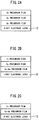
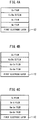
- FIGs. 2 to 4 A preferred embodiment of the thin-film solar cell production method disclosed in the present specification will now be described referring to FIGs. 2 to 4 .
- the first electrode layer 12 is formed on the substrate 11.
- the thickness of the first electrode layer 12 can be, for example, 200 to 500 nm.
- the first electrode layer 12 is formed by, for example, a DC sputtering method using Mo as a material.
- the p-type light absorption layer 13 containing a Group I-III-VI 2 compound is formed on the first electrode layer 12.
- Examples of a method of forming the p-type light absorption layer 13 include (1) a method of forming metal precursor films of a Group I element and Group III elements and subsequently forming a compound of the resulting metal precursor films and a Group VI element; and (2) a method of forming a film by vapor deposition using Group I, III and VI elements.
- the basic idea of the method (1) is to form, on the first electrode layer 12, first a Ga and Cu-containing precursor film and then an In-containing precursor film and subsequently form a compound composed of the Ga and Cu-containing precursor film, the In-containing precursor film and a Group VI element.
- a precursor film containing mixed crystals of Ga and Cu may be formed, or a Cu-containing precursor film may be laminated on a Ga-containing precursor film.
- the ratio C2 of the number of atoms between Cu and the Group III elements in the surface of the p-type light absorption layer 13 on the second electrode layer 15 side can be controlled to be 1.0 or higher and the ratio G2 of the number of atoms between Ga and the Group III elements in the surface on the second electrode layer 15 side can be controlled to be lower than 0.13. Further, the ratio G2 of the number of atoms between Ga and the Group III elements in the surface can also be reduced by shortening the time of a heat treatment performed for the formation of a compound with a Group VI element or by adding an alkali compound (for example, addition into a precursor film or diffusion from the substrate).
- a Ga precursor film is first formed on the first electrode layer 12, and a Cu precursor film and then an In precursor film are formed thereon.
- a Cu-Ga precursor film which is composed of mixed crystals of Ga and Cu, is first formed on the first electrode layer 12, and a Cu precursor film and then an In precursor film are formed thereon.
- a Cu-Ga precursor film which is composed of mixed crystals of Ga and Cu, is first formed on the first electrode layer 12, and an In precursor film is then formed thereon.
- Ga and Cu-containing precursor film includes films formed by laminating a Ga precursor film and a Cu precursor film as depicted in FIG. 2A as well as Cu-Ga precursor films composed of mixed crystals of Ga and Cu as depicted in FIG. 2C .
- the precursor films can each be formed by a known film-forming technology such as sputtering.
- the present inventors discovered that in the formation of a compound between a Cu-containing precursor film and Se which is a Group VI element, the Cu concentration in the surface of the precursor film can be controlled by adjusting the Se concentration in a reaction gas.
- the selenization process of forming a compound between a precursor film and Se is carried out based on this discovery.
- This Se concentration in the reaction gas used in the selenization process of forming a compound between a precursor film and Se is adjusted as described below.
- a compound composed of a precursor film for adjustment and Se which precursor film has the same structure as a laminated film in which a Ga and Cu-containing precursor film and an In precursor film are laminated as shown in FIGs. 2A to 2C , is formed and the ratio of the number of atoms between Cu and the Group III elements in the surface of the precursor film for adjustment is determined.
- the precursor film for adjustment is a film which is separately formed such that it has the same structure as a laminated film obtained by laminating a Ga and Cu-containing precursor film and an In precursor film.
- surface of the precursor film for adjustment means the part corresponding to the region 13a depicted in FIG. 1 .
- the ratio determined in the step S1 and the desired ratio of the number of atoms between Cu and the Group III elements are compared.
- the desired ratio of the number of atoms between Cu and the Group III elements is 1.0 or higher but preferably lower than 1.25.
- the process proceeds to the step S3.
- the ratio determined in the step S1 is higher than the desired ratio of the number of atoms between Cu and the Group III elements, the process proceeds to the step S4, or when the ratio determined in the step S1 is within an acceptable range with respect to the desired ratio of the number of atoms between Cu and the Group III elements, the process proceeds to the step S5.
- the Se concentration in the reaction gas is adjusted to be lower than the prescribed concentration. The process then proceeds to the step S6.
- the Se concentration in the reaction gas is adjusted to be higher than the prescribed concentration. The process then proceeds to the step S6.
- This other precursor film for adjustment is a film which is formed separately from the precursor film for adjustment used in the step 1.
- step S7 the ratio of the number of atoms between Cu and the Group III elements in the surface of this other precursor film for adjustment is determined.
- the process then returns to the step S2. Thereafter, the above-described operations of the steps S2 to S7 are repeated. It is noted here that the "prescribed concentration" in the steps S3 and S4 is replaceable with the adjusted concentration used in the step S6.
- the Se concentration of the reaction gas is already adjusted to yield a desired ratio C2. Then, using the reaction gas having the adjusted Se concentration, a compound is formed between a laminated film, in which a Ga and Cu-containing precursor film and an In precursor film are laminated, and Se under a prescribed temperature (selenization). In this manner, the ratio C2 of the number of atoms between Cu and the Group III elements in the surface of the p-type light absorption layer 13 on the second electrode layer 15 side can be controlled to be 1.0 or higher but preferably lower than 1.25. It is noted here that the adjusted Se concentration may vary depending on the reactor used for the reaction.
- the thus selenized laminated film is allowed to form a compound with S, which is a Group VI element (sulfurization).
- the ratio C1 of the number of atoms between Cu and the Group III elements in the entire p-type light absorption layer can be adjusted by controlling the number of Cu atoms and that of the Group III element atoms in the precursor films to be laminated, for example, by changing the thickness ratio of the Cu-Ga precursor film and the In precursor film or the thickness ratio of the Cu-Ga precursor film and the Cu precursor film.
- the basic idea of the method (2) is to form the p-type light absorption layer 13 by, in the vapor deposition on the first electrode layer 12 using Group I, III and VI elements as vapor deposition sources, performing vapor deposition of Ga before vapor deposition of In as vapor deposition of Group III elements so as to form a semiconductor layer having a chalcopyrite structure in which the ratio G2 of the number of atoms between Ga and the Group III elements (atomic ratio in the surface of the p-type light absorption layer 13) is lower than 0.13 and subsequently performing vapor deposition of Cu alone on the thus formed semiconductor layer.
- the ratio C2 of the number of atoms between Cu and the Group III elements in the surface of the p-type light absorption layer 13 on the second electrode layer 15 side can be controlled to be 1.0 or higher, but also the ratio G2 of the number of atoms between Ga and the Group III elements in the surface on the second electrode layer 15 side can be controlled to be lower than 0.13. Further, the ratio G2 of the number of atoms between Ga and the Group III elements in the surface can also be reduced by shortening the time of a heat treatment performed for the vapor deposition of a Group VI element or by adding an alkali compound (vapor deposition using an alkali compound as a vapor deposition source or diffusion of an alkali compound from the substrate).
- the p-type light absorption layer may also be formed by further vapor-depositing Cu, which is a Group I element, in the form of a vapor deposition film containing Cu and Ga or In or using a vapor deposition source containing Cu and S or Se.
- Cu which is a Group I element
- an Se film, an S film or an Se and S-containing film can be formed by vapor deposition on an In film.
- Ga is first vapor-deposited and In is subsequently vapor-deposited thereon. Then, Cu(Se,S) containing Se, S and Cu is vapor-deposited, and Cu alone is finally vapor-deposited.
- Cu(Se,S) containing Se, S and Cu is vapor-deposited, and Cu alone is finally vapor-deposited.
- a heat treatment may be performed so as to form a compound of Cu, Se or S, In and Ga.
- a vapor deposition source of Se and S In place of the vapor deposition of Cu(Se,S), a vapor deposition source of Se and S, an Se, S and Cu-containing vapor deposition source, or an Se and Cu-containing vapor deposition source and a vapor deposition source of S, can be used as well.
- a vapor deposition source of Se and S an Se, S and Cu-containing vapor deposition source, or an Se and Cu-containing vapor deposition source and a vapor deposition source of S
- a vapor deposition source of S for example, a multi-source simultaneous vapor deposition method can be employed.
- Cu and Ga are first vapor-deposited, and Cu and In (or a CuIn compound) are subsequently vapor-deposited thereon. Then, Se, S and Cu (or a CuSeS compound) are vapor-deposited and Cu alone is finally vapor-deposited.
- a heat treatment may be performed so as to form a compound of Cu, Se or S, In and Ga.
- Cu and Ga are first vapor-deposited, and Cu and In (or a CuIn compound) are subsequently vapor-deposited thereon. Then, Se and S (or an SeS compound) are vapor-deposited and Cu alone is finally vapor-deposited.
- a heat treatment may be performed so as to form a compound of Cu, Se or S, In and Ga.
- the buffer layer 14 is formed on the p-type light absorption layer 13 formed in the above-described manner.
- the buffer layer 14 for example, a transparent and high-resistance 2 to 50 nm-thick Zn(O,S,OH) x film having an n-type conductivity can be formed.
- This buffer layer 14 can be prepared by a chemical bath deposition method or an MOCVD method.
- a Group II-VI compound semiconductor thin film composed of CdS, ZnS, ZnO or the like, a film made of Zn(O,S) x or the like which is a mixed crystal of the above-described Group II-VI compounds, or an In-based compound semiconductor thin film composed of In 2 O 3 , In 2 S 3 , In(OH) x or the like can also be used.
- the second electrode layer 15 is formed.
- the second electrode layer 15 for example, a transparent and low-resistance 0.2 to 2.5 ⁇ m-thick conductive film which is composed of ZnO:B and has an n-type conductivity and a broad forbidden band width can be formed.
- This second electrode layer 15 can be prepared by a sputtering method or an MOCVD method.
- ZnO:Al or ZnO:Ga can be used, and a transparent conductive film composed of ITO may also be used.
- the thin-film solar cell of Example 1 was produced as described below.
- the first electrode layer 12 was formed by a sputtering method using Mo.
- the p-type light absorption layer 13 was formed by the above-described method (1).
- a Group I element Cu was used.
- Group III elements Ga and In were used and, as Group VI elements, Se and S were used.
- the p-type light absorption layer 13 was prepared by forming, as precursor films on the first electrode layer, first a CuGa film by a sputtering method, next a Cu film by a sputtering method and then an In film by a sputtering method. The resulting laminate of the thus formed precursor films was subjected to selenization and sulfurization.
- the buffer layer 14 was formed by a chemical bath deposition method using Zn(O,S,OH) x .
- the second electrode layer 15 was formed by an MOCVD method using ZnO:B (boron-doped zinc oxide).
- the ratio C1 of the number of atoms between Cu and the Group III elements in the entire p-type light absorption layer 13 was in a range of 0.86 to 0.98.
- the ratio C2 of the number of atoms between Cu and the Group III elements in the surface of the p-type light absorption layer 13 on the second electrode layer 15 side was 1.00.
- the ratio G1 of the number of atoms between Ga and the Group III elements in the entire p-type light absorption layer 13 was in a range of 0.35 to 0.45.
- the ratio G2 of the number of atoms between Ga and the Group III elements in the surface of the p-type light absorption layer 13 on the second electrode layer 15 side was 0.06. These ratios of the number of atoms were determined by measuring the number of the respective atoms by glow discharge spectrometry while grinding the sample surface by a sputtering method.
- Example 2 The thin-film solar cell of Example 2 was obtained in the same manner as in Example 1, except that the ratio C2 was 1.10 and the ratio G2 was 0.07.
- the ratio G2 of 0.07 is substantially the same as in Example 1; however, Example 2 is different from Example 1 in that the ratio of the number of atoms between Cu and the Group III elements in the formation of the precursor films was increased so as to control the ratio C2 to be 1.10.
- Example 3 The thin-film solar cell of Example 3 was obtained in the same manner as in Example 2, except that the ratio G2 was 0.13.
- Example 3 is different from Example 2 in that the processing time for the formation of the p-type light absorption layer, in other words, the time of the heat treatment performed for the formation of a compound with the Group VI elements, was made longer than that of Example 1 so as to control the ratio G2 to be 0.13.
- Comparative Example 1 The thin-film solar cell of Comparative Example 1 was obtained in the same manner as in Example 1, except that the ratio C2 was 0.94 and the ratio G2 was 0.10. Comparative Example 1 is different from Example 1 in that the selenium concentration in the selenization was increased as described below so as to control the ratio C2 to be 0.94 and that the processing time for the formation of the p-type light absorption layer was extended so as to control the ratio G2 to be 0.10.
- Comparative Example 2 The thin-film solar cell of Comparative Example 2 was obtained in the same manner as in Comparative Example 1, except that the ratio G2 was 0.18. Comparative Example 2 is different from Comparative Example 1 in that the processing time for the formation of the p-type light absorption layer was extended so as to control the ratio G2 to be 0.18.
- Comparative Example 3 The thin-film solar cell of Comparative Example 3 was obtained in the same manner as in Example 3, except that the ratio G2 was 0.15. Comparative Example 3 is different from Example 3 in that the processing time for the formation of the p-type light absorption layer was extended so as to control the ratio G2 to be 0.15.
- Comparative Example 4 The thin-film solar cell of Comparative Example 4 was obtained in the same manner as in Example 3, except that the ratio G2 was 0.24. Comparative Example 4 is different from Example 3 in that the processing time for the formation of the p-type light absorption layer was extended so as to control the ratio G2 to be 0.24.
- Comparative Example 5 The thin-film solar cell of Comparative Example 5 was obtained in the same manner as in Example 3, except that the ratio G2 was 0.35. Comparative Example 5 is different from Example 3 in that the processing time for the formation of the p-type light absorption layer was extended so as to control the ratio G2 to be 0.35.
- the H 2 Se concentration in the reaction gas used for selenization was 1.1% by volume and, in the process of producing the p-type light absorption layers of Examples 1 to 3 and Comparative Examples 3 to 5, the H 2 Se concentration in the reaction gas used for selenization was 0.9% by volume.
- the reaction gas a mixed gas of H 2 Se and nitrogen was used.
- the ratio C2 (1.00 to 1.10) was 1.0 or higher and the ratio G2 (0.06 to 0.13) was 0.13 or lower.
- the repeatability error in the measurement of the photoelectric conversion efficiency (Eff) is within about ⁇ 2% and at a photoelectric conversion efficiency (Eff) of 15%, the repeatability error is within about ⁇ 0.3%. Further, when the same thin-film solar cells are produced and their photoelectric conversion efficiencies (Eff) are measured, the error attributed to the reproducibility is affected by calcination and the like; therefore, this error may be larger than the repeatability error.
- the photoelectric conversion efficiency was not lower than 15.5%, which was higher by at least 0.5% than in any of Comparative Examples 1 to 5.
- the fill factor (FF) as well, the thin-film solar cells of Examples 1 to 3 exhibited a value equal to or higher than the values exhibited by the thin-film solar cells of Comparative Examples 1 to 5.
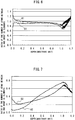
- FIG. 6 indicates the results of determining the relationship between the ratio, the number of Cu atoms/(the number of Ga + In atoms), and the depth of each p-type light absorption layer by measuring the number of Cu, Ga and In atoms based on glow discharge spectrometry while grinding the sample surface by a sputtering method.
- the value of "(the number of Ga + In atoms)" means the number of the Group III element atoms.
- the abscissa of FIG. 6 represents the depth of the p-type light absorption layer from the surface of the buffer layer side.
- a value of 0.0 on the abscissa corresponds to the position of the surface of the p-type light absorption layer on the buffer layer side, and a value of 1.0 on the abscissa corresponds to the position of the surface on the first electrode layer side.
- the ordinate of FIG. 6 represents the ratio, the number of Cu atoms/(the number of Ga + In atoms).
- the curve A1 represents the measurement results for Example 2, while the curve B1 represents the measurement results for Comparative Example 1.
- the curve A1 rises from a depth of about 0.1 (10% of the thickness of the p-type light absorption layer) toward a depth of 0.0 (the surface of the buffer layer side) and particularly, a rapid rise starts at a depth of about 0.05 (5% of the thickness of the p-type light absorption layer).
- the curve A1 indicates a value of 1.0 or greater at a depth of about 0.1 (10% of the thickness of the p-type light absorption layer), rising to a value of 1.1 or greater at a depth of about 0.05.
- the ratio C2 of the number of atoms between Cu and the Group III elements is 1.0 or higher in the part corresponding to 5% of the thickness of the p-type light absorption layer from the surface on the buffer layer side.
- the curve B1 indicates substantially constant values; however, it rapidly decreases from a depth of about 0.04 toward a depth of 0.0(the surface of the buffer layer side). Specifically, the curve B1 indicates values of about 0.9 throughout a depth of 1.0 to a depth of 0.04 but decreases to a value of less than 0.8 from a depth of 0.04 toward a depth of 0.0.
- FIG. 7 indicates the results of determining the relationship between the ratio, the number of Ga atoms/(the number of Ga + In atoms), and the depth of each p-type light absorption layer by measuring the number of Ga and In atoms based on glow discharge spectrometry while grinding the sample surface by a sputtering method.
- the abscissa of FIG. 7 represents the depth of the p-type light absorption layer from the surface of the buffer layer side.
- the value of 0.0 on the abscissa corresponds to the position of the surface of the p-type light absorption layer on the buffer layer side
- the value of 1.0 on the abscissa corresponds to the position of the surface on the first electrode layer side.
- the ordinate of FIG. 7 represents the ratio, the number of Ga atoms/(the number of Ga + In atoms).
- the curve A2 represents the measurement results for Example 1, while the curve B2 represents the measurement results for Comparative Example 5.
- the curve A2 indicates values of 0.1 or less throughout a depth of 0.20 to a depth of 0.0 (the surface of the buffer layer side). It is thus seen that in the p-type light absorption layer of Example 1, the ratio C2 of the number atoms between Ga and the Group III elements is 0.13 or lower in the part corresponding to 5% of the thickness of the p-type light absorption layer from the surface on the buffer layer side.
- the curve B2 indicates values of 0.2 or greater over the entirety of the depth direction.
- the ratio C2 (1.10) be 1.0 or higher and the ratio G2 (0.10) be 0.13 or lower as in Examples 1 to 3.
- the ratio G2 it is believed that by controlling the ratio G2 to be 0.13 or lower, the Ga concentration in the surface of the p-type light absorption layer 13 on the buffer layer 14 side is reduced and this consequently reduces defects acting as recombination centers, thereby the photoelectric conversion efficiency is improved.
- the thin-film solar cells and the methods of producing a thin-film solar cell according to the above-described embodiments can be modified as appropriate as long as the modification does not deviate from the gist of the present invention.
- the required constituents of one embodiment can be appropriately applied to other embodiments as well.
Landscapes
- Chemical & Material Sciences (AREA)
- Engineering & Computer Science (AREA)
- Chemical Kinetics & Catalysis (AREA)
- Materials Engineering (AREA)
- Mechanical Engineering (AREA)
- Metallurgy (AREA)
- Organic Chemistry (AREA)
- Inorganic Chemistry (AREA)
- Photovoltaic Devices (AREA)
- Manufacturing & Machinery (AREA)
- Life Sciences & Earth Sciences (AREA)
- Sustainable Energy (AREA)
Applications Claiming Priority (2)
| Application Number | Priority Date | Filing Date | Title |
|---|---|---|---|
| JP2013147092 | 2013-07-12 | ||
| PCT/JP2014/066310 WO2015005091A1 (ja) | 2013-07-12 | 2014-06-19 | 薄膜太陽電池及び薄膜太陽電池の製造方法 |
Publications (3)
| Publication Number | Publication Date |
|---|---|
| EP3021367A1 true EP3021367A1 (de) | 2016-05-18 |
| EP3021367A4 EP3021367A4 (de) | 2017-02-15 |
| EP3021367B1 EP3021367B1 (de) | 2020-06-03 |
Family
ID=52279777
Family Applications (1)
| Application Number | Title | Priority Date | Filing Date |
|---|---|---|---|
| EP14822465.2A Active EP3021367B1 (de) | 2013-07-12 | 2014-06-19 | Dünnschichtsolarzelle |
Country Status (4)
| Country | Link |
|---|---|
| US (1) | US9786804B2 (de) |
| EP (1) | EP3021367B1 (de) |
| JP (1) | JP6297038B2 (de) |
| WO (1) | WO2015005091A1 (de) |
Families Citing this family (4)
| Publication number | Priority date | Publication date | Assignee | Title |
|---|---|---|---|---|
| CN107848065B (zh) * | 2015-07-31 | 2020-03-13 | 国立大学法人大阪大学 | 摩擦焊接方法 |
| US10727366B2 (en) * | 2016-01-13 | 2020-07-28 | Mecaroenergy Co., Ltd. | Solar cell comprising CIGS light absorbing layer and method for manufacturing same |
| WO2020129803A1 (ja) * | 2018-12-19 | 2020-06-25 | 出光興産株式会社 | 光電変換素子および光電変換素子の製造方法 |
| JP7457310B1 (ja) | 2023-06-12 | 2024-03-28 | 株式会社Pxp | 薄膜太陽電池及び薄膜太陽電池の製造方法 |
Family Cites Families (13)
| Publication number | Priority date | Publication date | Assignee | Title |
|---|---|---|---|---|
| US5141564A (en) * | 1988-05-03 | 1992-08-25 | The Boeing Company | Mixed ternary heterojunction solar cell |
| JP3468328B2 (ja) * | 1996-01-29 | 2003-11-17 | 松下電器産業株式会社 | 半導体薄膜の製造方法 |
| JP3249407B2 (ja) | 1996-10-25 | 2002-01-21 | 昭和シェル石油株式会社 | カルコパイライト系多元化合物半導体薄膜光吸収層からなる薄膜太陽電池 |
| JP3249408B2 (ja) | 1996-10-25 | 2002-01-21 | 昭和シェル石油株式会社 | 薄膜太陽電池の薄膜光吸収層の製造方法及び製造装置 |
| JP2006049768A (ja) * | 2004-08-09 | 2006-02-16 | Showa Shell Sekiyu Kk | Cis系化合物半導体薄膜太陽電池及び該太陽電池の光吸収層の製造方法 |
| JP2007123532A (ja) * | 2005-10-27 | 2007-05-17 | Honda Motor Co Ltd | 太陽電池 |
| US8299510B2 (en) * | 2007-02-02 | 2012-10-30 | Rohm Co., Ltd. | Solid state imaging device and fabrication method for the same |
| US20130025660A1 (en) * | 2010-09-15 | 2013-01-31 | Precursor Energetics, Inc. | Processes for photovoltaic absorbers with compositional gradients |
| KR20120133342A (ko) * | 2011-05-31 | 2012-12-10 | 한국에너지기술연구원 | 균일한 Ga 분포를 갖는 CIGS 박막 제조방법 |
| US9184329B2 (en) * | 2011-06-22 | 2015-11-10 | Kyocera Corporation | Photoelectric conversion device |
| US8652870B2 (en) * | 2011-10-27 | 2014-02-18 | Intermolecular, Inc. | Method of fabricating CIGS by selenization at high temperature |
| JP2013115119A (ja) * | 2011-11-25 | 2013-06-10 | Nitto Denko Corp | 化合物太陽電池セルおよびその製法ならびにそれを用いた化合物太陽電池モジュールおよびその製法 |
| JP2014152085A (ja) * | 2013-02-12 | 2014-08-25 | Nitto Denko Corp | Cigs膜の製法およびその製法を用いるcigs太陽電池の製法 |
-
2014
- 2014-06-19 JP JP2015526237A patent/JP6297038B2/ja active Active
- 2014-06-19 WO PCT/JP2014/066310 patent/WO2015005091A1/ja not_active Ceased
- 2014-06-19 US US14/904,034 patent/US9786804B2/en active Active
- 2014-06-19 EP EP14822465.2A patent/EP3021367B1/de active Active
Also Published As
| Publication number | Publication date |
|---|---|
| JP6297038B2 (ja) | 2018-03-20 |
| WO2015005091A1 (ja) | 2015-01-15 |
| EP3021367B1 (de) | 2020-06-03 |
| JPWO2015005091A1 (ja) | 2017-03-02 |
| US9786804B2 (en) | 2017-10-10 |
| EP3021367A4 (de) | 2017-02-15 |
| US20160155878A1 (en) | 2016-06-02 |
Similar Documents
| Publication | Publication Date | Title |
|---|---|---|
| US9087954B2 (en) | Method for producing the pentanary compound semiconductor CZTSSe, and thin-film solar cell | |
| US8679893B2 (en) | Absorbers for high-efficiency thin-film PV | |
| EP2309548A2 (de) | Photoelektrische Umwandlungsvorrichtung, Herstellungsverfahren dafür und Solarbatterie | |
| US20140113403A1 (en) | High efficiency CZTSe by a two-step approach | |
| US8283187B2 (en) | Photovoltaic device and method for making | |
| EP2713404A2 (de) | Photoelektrisches Umwandlungselement und Solarzelle | |
| US20130164918A1 (en) | Absorbers For High-Efficiency Thin-Film PV | |
| KR20170122433A (ko) | 황화주석 박막 및 그 형성 방법, 박막 태양전지 및 그 제조방법 | |
| KR20130052478A (ko) | 태양전지 및 이의 제조방법 | |
| EP2988337A1 (de) | Solarzelle und verfahren zur herstellung einer solarzelle | |
| EP2768030A2 (de) | Solarzelle und Verfahren zu ihrer Herstellung | |
| EP3021367B1 (de) | Dünnschichtsolarzelle | |
| EP2784828A1 (de) | Czts-dünnfilmsolarzelle und herstellungsverfahren dafür | |
| US8916411B1 (en) | Absorber layer for a thin film photovoltaic device with a double-graded band gap | |
| US8859323B2 (en) | Method of chalcogenization to form high quality cigs for solar cell applications | |
| US20130344646A1 (en) | Absorbers for High-Efficiency Thin-Film PV | |
| JP5421752B2 (ja) | 化合物半導体太陽電池 | |
| EP2437289A2 (de) | Photovoltaikvorrichtung und Herstellungsverfahren | |
| EP3902018B1 (de) | Photoelektrisches umwandlungselement und verfahren zur herstellung des photoelektrischen umwandlungselements | |
| EP3238228B1 (de) | Verfahren zur herstellung eines schichtsystems für dünnschicht-solarzellen mit einer natrium-indium-sulfidpufferschicht | |
| WO2012091170A1 (en) | Solar cell and solar cell production method | |
| KR102015985B1 (ko) | 태양전지용 cigs 박막의 제조방법 | |
| US9899561B2 (en) | Method for producing a compound semiconductor, and thin-film solar cell | |
| WO2013031843A1 (ja) | 光電変換素子とその製造方法並びに光電変換装置 | |
| Nakamura | ELECTRODEPOSITION OF CUINSE2 |
Legal Events
| Date | Code | Title | Description |
|---|---|---|---|
| PUAI | Public reference made under article 153(3) epc to a published international application that has entered the european phase |
Free format text: ORIGINAL CODE: 0009012 |
|
| 17P | Request for examination filed |
Effective date: 20160108 |
|
| AK | Designated contracting states |
Kind code of ref document: A1 Designated state(s): AL AT BE BG CH CY CZ DE DK EE ES FI FR GB GR HR HU IE IS IT LI LT LU LV MC MK MT NL NO PL PT RO RS SE SI SK SM TR |
|
| AX | Request for extension of the european patent |
Extension state: BA ME |
|
| DAX | Request for extension of the european patent (deleted) | ||
| A4 | Supplementary search report drawn up and despatched |
Effective date: 20170117 |
|
| RIC1 | Information provided on ipc code assigned before grant |
Ipc: H01L 21/02 20060101ALI20170111BHEP Ipc: H01L 31/0392 20060101ALI20170111BHEP Ipc: H01L 31/065 20120101ALI20170111BHEP Ipc: H01L 31/032 20060101ALI20170111BHEP Ipc: H01L 31/18 20060101ALI20170111BHEP Ipc: C23C 14/06 20060101ALI20170111BHEP Ipc: H01L 31/0749 20120101AFI20170111BHEP |
|
| STAA | Information on the status of an ep patent application or granted ep patent |
Free format text: STATUS: EXAMINATION IS IN PROGRESS |
|
| 17Q | First examination report despatched |
Effective date: 20180213 |
|
| REG | Reference to a national code |
Ref country code: DE Ref legal event code: R079 Ref document number: 602014066299 Country of ref document: DE Free format text: PREVIOUS MAIN CLASS: H01L0031074900 Ipc: C23C0014580000 |
|
| GRAP | Despatch of communication of intention to grant a patent |
Free format text: ORIGINAL CODE: EPIDOSNIGR1 |
|
| STAA | Information on the status of an ep patent application or granted ep patent |
Free format text: STATUS: GRANT OF PATENT IS INTENDED |
|
| RIC1 | Information provided on ipc code assigned before grant |
Ipc: H01L 31/0392 20060101ALI20200128BHEP Ipc: H01L 31/065 20120101ALI20200128BHEP Ipc: C23C 14/18 20060101ALI20200128BHEP Ipc: H01L 31/0749 20120101ALI20200128BHEP Ipc: C23C 14/06 20060101ALI20200128BHEP Ipc: H01L 31/18 20060101ALI20200128BHEP Ipc: H01L 31/032 20060101ALI20200128BHEP Ipc: C23C 14/58 20060101AFI20200128BHEP Ipc: H01L 21/02 20060101ALI20200128BHEP |
|
| INTG | Intention to grant announced |
Effective date: 20200227 |
|
| GRAS | Grant fee paid |
Free format text: ORIGINAL CODE: EPIDOSNIGR3 |
|
| GRAA | (expected) grant |
Free format text: ORIGINAL CODE: 0009210 |
|
| STAA | Information on the status of an ep patent application or granted ep patent |
Free format text: STATUS: THE PATENT HAS BEEN GRANTED |
|
| AK | Designated contracting states |
Kind code of ref document: B1 Designated state(s): AL AT BE BG CH CY CZ DE DK EE ES FI FR GB GR HR HU IE IS IT LI LT LU LV MC MK MT NL NO PL PT RO RS SE SI SK SM TR |
|
| REG | Reference to a national code |
Ref country code: GB Ref legal event code: FG4D |
|
| REG | Reference to a national code |
Ref country code: CH Ref legal event code: EP Ref country code: AT Ref legal event code: REF Ref document number: 1277107 Country of ref document: AT Kind code of ref document: T Effective date: 20200615 |
|
| REG | Reference to a national code |
Ref country code: DE Ref legal event code: R096 Ref document number: 602014066299 Country of ref document: DE |
|
| REG | Reference to a national code |
Ref country code: LT Ref legal event code: MG4D |
|
| PG25 | Lapsed in a contracting state [announced via postgrant information from national office to epo] |
Ref country code: LT Free format text: LAPSE BECAUSE OF FAILURE TO SUBMIT A TRANSLATION OF THE DESCRIPTION OR TO PAY THE FEE WITHIN THE PRESCRIBED TIME-LIMIT Effective date: 20200603 Ref country code: FI Free format text: LAPSE BECAUSE OF FAILURE TO SUBMIT A TRANSLATION OF THE DESCRIPTION OR TO PAY THE FEE WITHIN THE PRESCRIBED TIME-LIMIT Effective date: 20200603 Ref country code: NO Free format text: LAPSE BECAUSE OF FAILURE TO SUBMIT A TRANSLATION OF THE DESCRIPTION OR TO PAY THE FEE WITHIN THE PRESCRIBED TIME-LIMIT Effective date: 20200903 Ref country code: GR Free format text: LAPSE BECAUSE OF FAILURE TO SUBMIT A TRANSLATION OF THE DESCRIPTION OR TO PAY THE FEE WITHIN THE PRESCRIBED TIME-LIMIT Effective date: 20200904 Ref country code: SE Free format text: LAPSE BECAUSE OF FAILURE TO SUBMIT A TRANSLATION OF THE DESCRIPTION OR TO PAY THE FEE WITHIN THE PRESCRIBED TIME-LIMIT Effective date: 20200603 |
|
| REG | Reference to a national code |
Ref country code: NL Ref legal event code: MP Effective date: 20200603 |
|
| PG25 | Lapsed in a contracting state [announced via postgrant information from national office to epo] |
Ref country code: BG Free format text: LAPSE BECAUSE OF FAILURE TO SUBMIT A TRANSLATION OF THE DESCRIPTION OR TO PAY THE FEE WITHIN THE PRESCRIBED TIME-LIMIT Effective date: 20200903 Ref country code: HR Free format text: LAPSE BECAUSE OF FAILURE TO SUBMIT A TRANSLATION OF THE DESCRIPTION OR TO PAY THE FEE WITHIN THE PRESCRIBED TIME-LIMIT Effective date: 20200603 Ref country code: RS Free format text: LAPSE BECAUSE OF FAILURE TO SUBMIT A TRANSLATION OF THE DESCRIPTION OR TO PAY THE FEE WITHIN THE PRESCRIBED TIME-LIMIT Effective date: 20200603 Ref country code: LV Free format text: LAPSE BECAUSE OF FAILURE TO SUBMIT A TRANSLATION OF THE DESCRIPTION OR TO PAY THE FEE WITHIN THE PRESCRIBED TIME-LIMIT Effective date: 20200603 |
|
| REG | Reference to a national code |
Ref country code: AT Ref legal event code: MK05 Ref document number: 1277107 Country of ref document: AT Kind code of ref document: T Effective date: 20200603 |
|
| PG25 | Lapsed in a contracting state [announced via postgrant information from national office to epo] |
Ref country code: NL Free format text: LAPSE BECAUSE OF FAILURE TO SUBMIT A TRANSLATION OF THE DESCRIPTION OR TO PAY THE FEE WITHIN THE PRESCRIBED TIME-LIMIT Effective date: 20200603 Ref country code: AL Free format text: LAPSE BECAUSE OF FAILURE TO SUBMIT A TRANSLATION OF THE DESCRIPTION OR TO PAY THE FEE WITHIN THE PRESCRIBED TIME-LIMIT Effective date: 20200603 |
|
| PG25 | Lapsed in a contracting state [announced via postgrant information from national office to epo] |
Ref country code: PT Free format text: LAPSE BECAUSE OF FAILURE TO SUBMIT A TRANSLATION OF THE DESCRIPTION OR TO PAY THE FEE WITHIN THE PRESCRIBED TIME-LIMIT Effective date: 20201006 Ref country code: RO Free format text: LAPSE BECAUSE OF FAILURE TO SUBMIT A TRANSLATION OF THE DESCRIPTION OR TO PAY THE FEE WITHIN THE PRESCRIBED TIME-LIMIT Effective date: 20200603 Ref country code: IT Free format text: LAPSE BECAUSE OF FAILURE TO SUBMIT A TRANSLATION OF THE DESCRIPTION OR TO PAY THE FEE WITHIN THE PRESCRIBED TIME-LIMIT Effective date: 20200603 Ref country code: SM Free format text: LAPSE BECAUSE OF FAILURE TO SUBMIT A TRANSLATION OF THE DESCRIPTION OR TO PAY THE FEE WITHIN THE PRESCRIBED TIME-LIMIT Effective date: 20200603 Ref country code: EE Free format text: LAPSE BECAUSE OF FAILURE TO SUBMIT A TRANSLATION OF THE DESCRIPTION OR TO PAY THE FEE WITHIN THE PRESCRIBED TIME-LIMIT Effective date: 20200603 Ref country code: ES Free format text: LAPSE BECAUSE OF FAILURE TO SUBMIT A TRANSLATION OF THE DESCRIPTION OR TO PAY THE FEE WITHIN THE PRESCRIBED TIME-LIMIT Effective date: 20200603 Ref country code: CZ Free format text: LAPSE BECAUSE OF FAILURE TO SUBMIT A TRANSLATION OF THE DESCRIPTION OR TO PAY THE FEE WITHIN THE PRESCRIBED TIME-LIMIT Effective date: 20200603 Ref country code: AT Free format text: LAPSE BECAUSE OF FAILURE TO SUBMIT A TRANSLATION OF THE DESCRIPTION OR TO PAY THE FEE WITHIN THE PRESCRIBED TIME-LIMIT Effective date: 20200603 |
|
| REG | Reference to a national code |
Ref country code: CH Ref legal event code: PL |
|
| PG25 | Lapsed in a contracting state [announced via postgrant information from national office to epo] |
Ref country code: SK Free format text: LAPSE BECAUSE OF FAILURE TO SUBMIT A TRANSLATION OF THE DESCRIPTION OR TO PAY THE FEE WITHIN THE PRESCRIBED TIME-LIMIT Effective date: 20200603 Ref country code: PL Free format text: LAPSE BECAUSE OF FAILURE TO SUBMIT A TRANSLATION OF THE DESCRIPTION OR TO PAY THE FEE WITHIN THE PRESCRIBED TIME-LIMIT Effective date: 20200603 Ref country code: IS Free format text: LAPSE BECAUSE OF FAILURE TO SUBMIT A TRANSLATION OF THE DESCRIPTION OR TO PAY THE FEE WITHIN THE PRESCRIBED TIME-LIMIT Effective date: 20201003 |
|
| REG | Reference to a national code |
Ref country code: DE Ref legal event code: R097 Ref document number: 602014066299 Country of ref document: DE |
|
| PG25 | Lapsed in a contracting state [announced via postgrant information from national office to epo] |
Ref country code: MC Free format text: LAPSE BECAUSE OF FAILURE TO SUBMIT A TRANSLATION OF THE DESCRIPTION OR TO PAY THE FEE WITHIN THE PRESCRIBED TIME-LIMIT Effective date: 20200603 Ref country code: LU Free format text: LAPSE BECAUSE OF NON-PAYMENT OF DUE FEES Effective date: 20200619 |
|
| PLBE | No opposition filed within time limit |
Free format text: ORIGINAL CODE: 0009261 |
|
| STAA | Information on the status of an ep patent application or granted ep patent |
Free format text: STATUS: NO OPPOSITION FILED WITHIN TIME LIMIT |
|
| REG | Reference to a national code |
Ref country code: BE Ref legal event code: MM Effective date: 20200630 |
|
| PG25 | Lapsed in a contracting state [announced via postgrant information from national office to epo] |
Ref country code: LI Free format text: LAPSE BECAUSE OF NON-PAYMENT OF DUE FEES Effective date: 20200630 Ref country code: FR Free format text: LAPSE BECAUSE OF NON-PAYMENT OF DUE FEES Effective date: 20200803 Ref country code: DK Free format text: LAPSE BECAUSE OF FAILURE TO SUBMIT A TRANSLATION OF THE DESCRIPTION OR TO PAY THE FEE WITHIN THE PRESCRIBED TIME-LIMIT Effective date: 20200603 Ref country code: CH Free format text: LAPSE BECAUSE OF NON-PAYMENT OF DUE FEES Effective date: 20200630 Ref country code: IE Free format text: LAPSE BECAUSE OF NON-PAYMENT OF DUE FEES Effective date: 20200619 |
|
| 26N | No opposition filed |
Effective date: 20210304 |
|
| GBPC | Gb: european patent ceased through non-payment of renewal fee |
Effective date: 20200903 |
|
| PG25 | Lapsed in a contracting state [announced via postgrant information from national office to epo] |
Ref country code: BE Free format text: LAPSE BECAUSE OF NON-PAYMENT OF DUE FEES Effective date: 20200630 Ref country code: SI Free format text: LAPSE BECAUSE OF FAILURE TO SUBMIT A TRANSLATION OF THE DESCRIPTION OR TO PAY THE FEE WITHIN THE PRESCRIBED TIME-LIMIT Effective date: 20200603 |
|
| PG25 | Lapsed in a contracting state [announced via postgrant information from national office to epo] |
Ref country code: GB Free format text: LAPSE BECAUSE OF NON-PAYMENT OF DUE FEES Effective date: 20200903 |
|
| PG25 | Lapsed in a contracting state [announced via postgrant information from national office to epo] |
Ref country code: TR Free format text: LAPSE BECAUSE OF FAILURE TO SUBMIT A TRANSLATION OF THE DESCRIPTION OR TO PAY THE FEE WITHIN THE PRESCRIBED TIME-LIMIT Effective date: 20200603 Ref country code: MT Free format text: LAPSE BECAUSE OF FAILURE TO SUBMIT A TRANSLATION OF THE DESCRIPTION OR TO PAY THE FEE WITHIN THE PRESCRIBED TIME-LIMIT Effective date: 20200603 Ref country code: CY Free format text: LAPSE BECAUSE OF FAILURE TO SUBMIT A TRANSLATION OF THE DESCRIPTION OR TO PAY THE FEE WITHIN THE PRESCRIBED TIME-LIMIT Effective date: 20200603 |
|
| PG25 | Lapsed in a contracting state [announced via postgrant information from national office to epo] |
Ref country code: MK Free format text: LAPSE BECAUSE OF FAILURE TO SUBMIT A TRANSLATION OF THE DESCRIPTION OR TO PAY THE FEE WITHIN THE PRESCRIBED TIME-LIMIT Effective date: 20200603 |
|
| PGFP | Annual fee paid to national office [announced via postgrant information from national office to epo] |
Ref country code: DE Payment date: 20250429 Year of fee payment: 12 |