EP3023425B1 - Verbindung, organisches optoelektronisches element damit und anzeigevorrichtung - Google Patents
Verbindung, organisches optoelektronisches element damit und anzeigevorrichtung Download PDFInfo
- Publication number
- EP3023425B1 EP3023425B1 EP13889161.9A EP13889161A EP3023425B1 EP 3023425 B1 EP3023425 B1 EP 3023425B1 EP 13889161 A EP13889161 A EP 13889161A EP 3023425 B1 EP3023425 B1 EP 3023425B1
- Authority
- EP
- European Patent Office
- Prior art keywords
- substituted
- unsubstituted
- group
- compound
- chemical formula
- Prior art date
- Legal status (The legal status is an assumption and is not a legal conclusion. Google has not performed a legal analysis and makes no representation as to the accuracy of the status listed.)
- Active
Links
- 0 CC(*1C(C=CC(C2)C3=CCC(*C4C=CC=CC44)C4=C3)=C2C(C)(C)C2=C1C(C1*)*1C=C2)C1C=CC(C)CCC1 Chemical compound CC(*1C(C=CC(C2)C3=CCC(*C4C=CC=CC44)C4=C3)=C2C(C)(C)C2=C1C(C1*)*1C=C2)C1C=CC(C)CCC1 0.000 description 5
- XSDKKRKTDZMKCH-UHFFFAOYSA-N Brc(cc1)ccc1-[n]1c(cccc2)c2c2c1cccc2 Chemical compound Brc(cc1)ccc1-[n]1c(cccc2)c2c2c1cccc2 XSDKKRKTDZMKCH-UHFFFAOYSA-N 0.000 description 2
- QDFNBGAWCUWFHT-UHFFFAOYSA-N [O-][N+](c(cccc1)c1-[n]1c(-c2ccncc2)nc2ccccc12)=O Chemical compound [O-][N+](c(cccc1)c1-[n]1c(-c2ccncc2)nc2ccccc12)=O QDFNBGAWCUWFHT-UHFFFAOYSA-N 0.000 description 2
- LWASRVWRPHNIDA-UHFFFAOYSA-N c(cc1)cc(c2c3cccc2)c1[n]3-c(cc1)ccc1N1c(cccc2)c2-[n]2c(-c3ccncc3)nc3cccc1c23 Chemical compound c(cc1)cc(c2c3cccc2)c1[n]3-c(cc1)ccc1N1c(cccc2)c2-[n]2c(-c3ccncc3)nc3cccc1c23 LWASRVWRPHNIDA-UHFFFAOYSA-N 0.000 description 2
- LBHGHMSXTCUPPA-UHFFFAOYSA-N CC(C)(c(cc(cc1)Cl)c1-[n]1c(-c2ccncc2)nc2c1cccc2)O Chemical compound CC(C)(c(cc(cc1)Cl)c1-[n]1c(-c2ccncc2)nc2c1cccc2)O LBHGHMSXTCUPPA-UHFFFAOYSA-N 0.000 description 1
- CPMSTYRUYWOIJE-UHFFFAOYSA-N CC1(C)c(ccc(Cl)c2)c2-[n]2c(-c3ccccc3)nc3cccc1c23 Chemical compound CC1(C)c(ccc(Cl)c2)c2-[n]2c(-c3ccccc3)nc3cccc1c23 CPMSTYRUYWOIJE-UHFFFAOYSA-N 0.000 description 1
- GEYOCULIXLDCMW-UHFFFAOYSA-N Nc(cccc1)c1N Chemical compound Nc(cccc1)c1N GEYOCULIXLDCMW-UHFFFAOYSA-N 0.000 description 1
- VQVJMSMIMXHFNL-UHFFFAOYSA-N Nc1ccccc1Nc(cccc1)c1[N+]([O-])=O Chemical compound Nc1ccccc1Nc(cccc1)c1[N+]([O-])=O VQVJMSMIMXHFNL-UHFFFAOYSA-N 0.000 description 1
- BGUWFUQJCDRPTL-UHFFFAOYSA-N O=Cc1ccncc1 Chemical compound O=Cc1ccncc1 BGUWFUQJCDRPTL-UHFFFAOYSA-N 0.000 description 1
- ORPVVAKYSXQCJI-UHFFFAOYSA-N [O-][N+](c(cccc1)c1Br)=O Chemical compound [O-][N+](c(cccc1)c1Br)=O ORPVVAKYSXQCJI-UHFFFAOYSA-N 0.000 description 1
- PWXANJHWUNUZTM-UHFFFAOYSA-N c(cc1)cc(N2)c1-[n]1c(-c3ccncc3)nc3c1c2ccc3 Chemical compound c(cc1)cc(N2)c1-[n]1c(-c3ccncc3)nc3c1c2ccc3 PWXANJHWUNUZTM-UHFFFAOYSA-N 0.000 description 1
- FTUMXLCQLMEZKN-UHFFFAOYSA-N c(cc1)ccc1-c1nc2c3[n]1-c(cccc1)c1Nc3ccc2 Chemical compound c(cc1)ccc1-c1nc2c3[n]1-c(cccc1)c1Nc3ccc2 FTUMXLCQLMEZKN-UHFFFAOYSA-N 0.000 description 1
- NBBCPISRCDWVEZ-UHFFFAOYSA-N c(cc1)ccc1-c1nc2cccc3c2[n]1-c1ccccc1N3c(cc1)ccc1-[n]1c2ccccc2c2c1cccc2 Chemical compound c(cc1)ccc1-c1nc2cccc3c2[n]1-c1ccccc1N3c(cc1)ccc1-[n]1c2ccccc2c2c1cccc2 NBBCPISRCDWVEZ-UHFFFAOYSA-N 0.000 description 1
Images

Classifications
-
- H—ELECTRICITY
- H10—SEMICONDUCTOR DEVICES; ELECTRIC SOLID-STATE DEVICES NOT OTHERWISE PROVIDED FOR
- H10K—ORGANIC ELECTRIC SOLID-STATE DEVICES
- H10K85/00—Organic materials used in the body or electrodes of devices covered by this subclass
- H10K85/60—Organic compounds having low molecular weight
- H10K85/649—Aromatic compounds comprising a hetero atom
- H10K85/657—Polycyclic condensed heteroaromatic hydrocarbons
-
- C—CHEMISTRY; METALLURGY
- C07—ORGANIC CHEMISTRY
- C07D—HETEROCYCLIC COMPOUNDS
- C07D471/00—Heterocyclic compounds containing nitrogen atoms as the only ring hetero atoms in the condensed system, at least one ring being a six-membered ring with one nitrogen atom, not provided for by groups C07D451/00 - C07D463/00
- C07D471/02—Heterocyclic compounds containing nitrogen atoms as the only ring hetero atoms in the condensed system, at least one ring being a six-membered ring with one nitrogen atom, not provided for by groups C07D451/00 - C07D463/00 in which the condensed system contains two hetero rings
- C07D471/04—Ortho-condensed systems
-
- C—CHEMISTRY; METALLURGY
- C07—ORGANIC CHEMISTRY
- C07D—HETEROCYCLIC COMPOUNDS
- C07D401/00—Heterocyclic compounds containing two or more hetero rings, having nitrogen atoms as the only ring hetero atoms, at least one ring being a six-membered ring with only one nitrogen atom
- C07D401/14—Heterocyclic compounds containing two or more hetero rings, having nitrogen atoms as the only ring hetero atoms, at least one ring being a six-membered ring with only one nitrogen atom containing three or more hetero rings
-
- C—CHEMISTRY; METALLURGY
- C07—ORGANIC CHEMISTRY
- C07D—HETEROCYCLIC COMPOUNDS
- C07D471/00—Heterocyclic compounds containing nitrogen atoms as the only ring hetero atoms in the condensed system, at least one ring being a six-membered ring with one nitrogen atom, not provided for by groups C07D451/00 - C07D463/00
- C07D471/02—Heterocyclic compounds containing nitrogen atoms as the only ring hetero atoms in the condensed system, at least one ring being a six-membered ring with one nitrogen atom, not provided for by groups C07D451/00 - C07D463/00 in which the condensed system contains two hetero rings
- C07D471/06—Peri-condensed systems
-
- C—CHEMISTRY; METALLURGY
- C07—ORGANIC CHEMISTRY
- C07D—HETEROCYCLIC COMPOUNDS
- C07D487/00—Heterocyclic compounds containing nitrogen atoms as the only ring hetero atoms in the condensed system, not provided for by groups C07D451/00 - C07D477/00
- C07D487/02—Heterocyclic compounds containing nitrogen atoms as the only ring hetero atoms in the condensed system, not provided for by groups C07D451/00 - C07D477/00 in which the condensed system contains two hetero rings
- C07D487/04—Ortho-condensed systems
-
- C—CHEMISTRY; METALLURGY
- C07—ORGANIC CHEMISTRY
- C07D—HETEROCYCLIC COMPOUNDS
- C07D487/00—Heterocyclic compounds containing nitrogen atoms as the only ring hetero atoms in the condensed system, not provided for by groups C07D451/00 - C07D477/00
- C07D487/02—Heterocyclic compounds containing nitrogen atoms as the only ring hetero atoms in the condensed system, not provided for by groups C07D451/00 - C07D477/00 in which the condensed system contains two hetero rings
- C07D487/06—Peri-condensed systems
-
- C—CHEMISTRY; METALLURGY
- C09—DYES; PAINTS; POLISHES; NATURAL RESINS; ADHESIVES; COMPOSITIONS NOT OTHERWISE PROVIDED FOR; APPLICATIONS OF MATERIALS NOT OTHERWISE PROVIDED FOR
- C09K—MATERIALS FOR MISCELLANEOUS APPLICATIONS, NOT PROVIDED FOR ELSEWHERE
- C09K11/00—Luminescent materials, e.g. electroluminescent or chemiluminescent
- C09K11/02—Use of particular materials as binders, particle coatings or suspension media therefor
- C09K11/025—Use of particular materials as binders, particle coatings or suspension media therefor non-luminescent particle coatings or suspension media
-
- C—CHEMISTRY; METALLURGY
- C09—DYES; PAINTS; POLISHES; NATURAL RESINS; ADHESIVES; COMPOSITIONS NOT OTHERWISE PROVIDED FOR; APPLICATIONS OF MATERIALS NOT OTHERWISE PROVIDED FOR
- C09K—MATERIALS FOR MISCELLANEOUS APPLICATIONS, NOT PROVIDED FOR ELSEWHERE
- C09K11/00—Luminescent materials, e.g. electroluminescent or chemiluminescent
- C09K11/06—Luminescent materials, e.g. electroluminescent or chemiluminescent containing organic luminescent materials
-
- H—ELECTRICITY
- H10—SEMICONDUCTOR DEVICES; ELECTRIC SOLID-STATE DEVICES NOT OTHERWISE PROVIDED FOR
- H10K—ORGANIC ELECTRIC SOLID-STATE DEVICES
- H10K50/00—Organic light-emitting devices
- H10K50/10—OLEDs or polymer light-emitting diodes [PLED]
- H10K50/11—OLEDs or polymer light-emitting diodes [PLED] characterised by the electroluminescent [EL] layers
-
- H—ELECTRICITY
- H10—SEMICONDUCTOR DEVICES; ELECTRIC SOLID-STATE DEVICES NOT OTHERWISE PROVIDED FOR
- H10K—ORGANIC ELECTRIC SOLID-STATE DEVICES
- H10K50/00—Organic light-emitting devices
- H10K50/10—OLEDs or polymer light-emitting diodes [PLED]
- H10K50/11—OLEDs or polymer light-emitting diodes [PLED] characterised by the electroluminescent [EL] layers
- H10K50/12—OLEDs or polymer light-emitting diodes [PLED] characterised by the electroluminescent [EL] layers comprising dopants
-
- H—ELECTRICITY
- H10—SEMICONDUCTOR DEVICES; ELECTRIC SOLID-STATE DEVICES NOT OTHERWISE PROVIDED FOR
- H10K—ORGANIC ELECTRIC SOLID-STATE DEVICES
- H10K59/00—Integrated devices, or assemblies of multiple devices, comprising at least one organic light-emitting element covered by group H10K50/00
- H10K59/10—OLED displays
- H10K59/12—Active-matrix OLED [AMOLED] displays
-
- H—ELECTRICITY
- H10—SEMICONDUCTOR DEVICES; ELECTRIC SOLID-STATE DEVICES NOT OTHERWISE PROVIDED FOR
- H10K—ORGANIC ELECTRIC SOLID-STATE DEVICES
- H10K85/00—Organic materials used in the body or electrodes of devices covered by this subclass
- H10K85/60—Organic compounds having low molecular weight
- H10K85/615—Polycyclic condensed aromatic hydrocarbons, e.g. anthracene
- H10K85/622—Polycyclic condensed aromatic hydrocarbons, e.g. anthracene containing four rings, e.g. pyrene
-
- H—ELECTRICITY
- H10—SEMICONDUCTOR DEVICES; ELECTRIC SOLID-STATE DEVICES NOT OTHERWISE PROVIDED FOR
- H10K—ORGANIC ELECTRIC SOLID-STATE DEVICES
- H10K85/00—Organic materials used in the body or electrodes of devices covered by this subclass
- H10K85/60—Organic compounds having low molecular weight
- H10K85/631—Amine compounds having at least two aryl rest on at least one amine-nitrogen atom, e.g. triphenylamine
-
- H—ELECTRICITY
- H10—SEMICONDUCTOR DEVICES; ELECTRIC SOLID-STATE DEVICES NOT OTHERWISE PROVIDED FOR
- H10K—ORGANIC ELECTRIC SOLID-STATE DEVICES
- H10K85/00—Organic materials used in the body or electrodes of devices covered by this subclass
- H10K85/60—Organic compounds having low molecular weight
- H10K85/649—Aromatic compounds comprising a hetero atom
-
- H—ELECTRICITY
- H10—SEMICONDUCTOR DEVICES; ELECTRIC SOLID-STATE DEVICES NOT OTHERWISE PROVIDED FOR
- H10K—ORGANIC ELECTRIC SOLID-STATE DEVICES
- H10K85/00—Organic materials used in the body or electrodes of devices covered by this subclass
- H10K85/60—Organic compounds having low molecular weight
- H10K85/649—Aromatic compounds comprising a hetero atom
- H10K85/654—Aromatic compounds comprising a hetero atom comprising only nitrogen as heteroatom
-
- H—ELECTRICITY
- H10—SEMICONDUCTOR DEVICES; ELECTRIC SOLID-STATE DEVICES NOT OTHERWISE PROVIDED FOR
- H10K—ORGANIC ELECTRIC SOLID-STATE DEVICES
- H10K85/00—Organic materials used in the body or electrodes of devices covered by this subclass
- H10K85/60—Organic compounds having low molecular weight
- H10K85/649—Aromatic compounds comprising a hetero atom
- H10K85/657—Polycyclic condensed heteroaromatic hydrocarbons
- H10K85/6572—Polycyclic condensed heteroaromatic hydrocarbons comprising only nitrogen in the heteroaromatic polycondensed ring system, e.g. phenanthroline or carbazole
-
- H—ELECTRICITY
- H10—SEMICONDUCTOR DEVICES; ELECTRIC SOLID-STATE DEVICES NOT OTHERWISE PROVIDED FOR
- H10K—ORGANIC ELECTRIC SOLID-STATE DEVICES
- H10K85/00—Organic materials used in the body or electrodes of devices covered by this subclass
- H10K85/60—Organic compounds having low molecular weight
- H10K85/649—Aromatic compounds comprising a hetero atom
- H10K85/657—Polycyclic condensed heteroaromatic hydrocarbons
- H10K85/6576—Polycyclic condensed heteroaromatic hydrocarbons comprising only sulfur in the heteroaromatic polycondensed ring system, e.g. benzothiophene
-
- C—CHEMISTRY; METALLURGY
- C09—DYES; PAINTS; POLISHES; NATURAL RESINS; ADHESIVES; COMPOSITIONS NOT OTHERWISE PROVIDED FOR; APPLICATIONS OF MATERIALS NOT OTHERWISE PROVIDED FOR
- C09K—MATERIALS FOR MISCELLANEOUS APPLICATIONS, NOT PROVIDED FOR ELSEWHERE
- C09K2211/00—Chemical nature of organic luminescent or tenebrescent compounds
- C09K2211/10—Non-macromolecular compounds
- C09K2211/1003—Carbocyclic compounds
- C09K2211/1007—Non-condensed systems
-
- C—CHEMISTRY; METALLURGY
- C09—DYES; PAINTS; POLISHES; NATURAL RESINS; ADHESIVES; COMPOSITIONS NOT OTHERWISE PROVIDED FOR; APPLICATIONS OF MATERIALS NOT OTHERWISE PROVIDED FOR
- C09K—MATERIALS FOR MISCELLANEOUS APPLICATIONS, NOT PROVIDED FOR ELSEWHERE
- C09K2211/00—Chemical nature of organic luminescent or tenebrescent compounds
- C09K2211/10—Non-macromolecular compounds
- C09K2211/1003—Carbocyclic compounds
- C09K2211/1011—Condensed systems
-
- C—CHEMISTRY; METALLURGY
- C09—DYES; PAINTS; POLISHES; NATURAL RESINS; ADHESIVES; COMPOSITIONS NOT OTHERWISE PROVIDED FOR; APPLICATIONS OF MATERIALS NOT OTHERWISE PROVIDED FOR
- C09K—MATERIALS FOR MISCELLANEOUS APPLICATIONS, NOT PROVIDED FOR ELSEWHERE
- C09K2211/00—Chemical nature of organic luminescent or tenebrescent compounds
- C09K2211/10—Non-macromolecular compounds
- C09K2211/1018—Heterocyclic compounds
- C09K2211/1025—Heterocyclic compounds characterised by ligands
- C09K2211/1029—Heterocyclic compounds characterised by ligands containing one nitrogen atom as the heteroatom
-
- C—CHEMISTRY; METALLURGY
- C09—DYES; PAINTS; POLISHES; NATURAL RESINS; ADHESIVES; COMPOSITIONS NOT OTHERWISE PROVIDED FOR; APPLICATIONS OF MATERIALS NOT OTHERWISE PROVIDED FOR
- C09K—MATERIALS FOR MISCELLANEOUS APPLICATIONS, NOT PROVIDED FOR ELSEWHERE
- C09K2211/00—Chemical nature of organic luminescent or tenebrescent compounds
- C09K2211/10—Non-macromolecular compounds
- C09K2211/1018—Heterocyclic compounds
- C09K2211/1025—Heterocyclic compounds characterised by ligands
- C09K2211/1044—Heterocyclic compounds characterised by ligands containing two nitrogen atoms as heteroatoms
-
- C—CHEMISTRY; METALLURGY
- C09—DYES; PAINTS; POLISHES; NATURAL RESINS; ADHESIVES; COMPOSITIONS NOT OTHERWISE PROVIDED FOR; APPLICATIONS OF MATERIALS NOT OTHERWISE PROVIDED FOR
- C09K—MATERIALS FOR MISCELLANEOUS APPLICATIONS, NOT PROVIDED FOR ELSEWHERE
- C09K2211/00—Chemical nature of organic luminescent or tenebrescent compounds
- C09K2211/10—Non-macromolecular compounds
- C09K2211/1018—Heterocyclic compounds
- C09K2211/1025—Heterocyclic compounds characterised by ligands
- C09K2211/1059—Heterocyclic compounds characterised by ligands containing three nitrogen atoms as heteroatoms
-
- C—CHEMISTRY; METALLURGY
- C09—DYES; PAINTS; POLISHES; NATURAL RESINS; ADHESIVES; COMPOSITIONS NOT OTHERWISE PROVIDED FOR; APPLICATIONS OF MATERIALS NOT OTHERWISE PROVIDED FOR
- C09K—MATERIALS FOR MISCELLANEOUS APPLICATIONS, NOT PROVIDED FOR ELSEWHERE
- C09K2211/00—Chemical nature of organic luminescent or tenebrescent compounds
- C09K2211/10—Non-macromolecular compounds
- C09K2211/1018—Heterocyclic compounds
- C09K2211/1025—Heterocyclic compounds characterised by ligands
- C09K2211/1088—Heterocyclic compounds characterised by ligands containing oxygen as the only heteroatom
-
- C—CHEMISTRY; METALLURGY
- C09—DYES; PAINTS; POLISHES; NATURAL RESINS; ADHESIVES; COMPOSITIONS NOT OTHERWISE PROVIDED FOR; APPLICATIONS OF MATERIALS NOT OTHERWISE PROVIDED FOR
- C09K—MATERIALS FOR MISCELLANEOUS APPLICATIONS, NOT PROVIDED FOR ELSEWHERE
- C09K2211/00—Chemical nature of organic luminescent or tenebrescent compounds
- C09K2211/10—Non-macromolecular compounds
- C09K2211/1018—Heterocyclic compounds
- C09K2211/1025—Heterocyclic compounds characterised by ligands
- C09K2211/1092—Heterocyclic compounds characterised by ligands containing sulfur as the only heteroatom
-
- H—ELECTRICITY
- H10—SEMICONDUCTOR DEVICES; ELECTRIC SOLID-STATE DEVICES NOT OTHERWISE PROVIDED FOR
- H10K—ORGANIC ELECTRIC SOLID-STATE DEVICES
- H10K2101/00—Properties of the organic materials covered by group H10K85/00
- H10K2101/10—Triplet emission
-
- H—ELECTRICITY
- H10—SEMICONDUCTOR DEVICES; ELECTRIC SOLID-STATE DEVICES NOT OTHERWISE PROVIDED FOR
- H10K—ORGANIC ELECTRIC SOLID-STATE DEVICES
- H10K85/00—Organic materials used in the body or electrodes of devices covered by this subclass
- H10K85/30—Coordination compounds
- H10K85/341—Transition metal complexes, e.g. Ru(II)polypyridine complexes
- H10K85/342—Transition metal complexes, e.g. Ru(II)polypyridine complexes comprising iridium
Definitions
- a compound, an organic optoelectronic device including the same and a display device are disclosed.
- An organic optoelectronic device is a device that converts electrical energy into photoenergy, and vice versa.
- An organic optoelectronic device may be classified as follows in accordance with its driving principles.
- One is an optoelectronic device where excitons are generated by photoenergy, separated into electrons and holes the electrons and holes, and are transferred to different electrodes to generate electrical energy
- the other is a light emitting device where a voltage or a current is supplied to an electrode to generate photoenergy from electrical energy.
- Examples of an organic optoelectronic device may be an organic photoelectric device, an organic light emitting diode, an organic solar cell and an organic photo conductor drum.
- an organic light emitting diode (OLED) has recently drawn attention due to an increase in demand for flat panel displays.
- Such an organic light emitting diode converts electrical energy into light by applying current to an organic light emitting material. It has a structure in which an organic layer is interposed between an anode and a cathode.
- an organic layer may include an emission layer and optionally an auxiliary layer, and the auxiliary layer may include, for example at least one selected from a hole injection layer, a hole transport layer, an electron blocking layer, an electron transport layer, an electron injection layer, and a hole blocking layer in order increase efficiency and stability of an organic light emitting diode.
- Performance of an organic light emitting diode may be affected by characteristics of the organic layer, and among them, may be mainly affected by characteristics of an organic material of the organic layer.
- substrates for electrochromic recording materials comprising a support sheet containing as color forming substances compounds of a certain structure, namely 1-R-4-(N-R-CO)amino-8-[N-(R 1 )(R 2 )amino]-9-R 3 -imidoxophenoxazines.
- One embodiment provides a compound being capable of realizing an organic optoelectronic device having high efficiency and long life-span.
- An organic optoelectronic device including the compound and a display device including the organic optoelectronic device are provided.
- L is a substituted or unsubstituted C6 to C30 arylene group, or a substituted or unsubstituted C2 to C30 heteroarylene group
- m is an integer of 1
- Ar is a substituted or unsubstituted C6 to C30 aryl group or a substituted or unsubstituted C2 to C30 heteroaryl group
- X is O, S, NR'or CR'R", the R' and R " are independently hydrogen, deuterium, a substituted or unsubstituted C1 to C20 alkyl group, a substituted or unsubstituted C6 to C30 aryl group, a substituted or unsubstituted C2 to C30 heteroaryl group, or a combination thereof
- R 1 and R 2 are each independently hydrogen, deuterium, a substituted or unsubstituted C1 to C20 alkyl group, a substituted or unsubstituted C6 to C30 aryl
- an organic optoelectronic device in another embodiment, includes an anode and a cathode facing each other; and at least one organic layer between the anode and the cathode, wherein the organic layer includes the compound according to one embodiment of the present invention.
- a display device including the organic optoelectronic device according to one embodiment of the present invention is provided.
- An organic optoelectronic device having high efficiency and long life-span may be realized.
- FIGS. 1 and 2 are cross-sectional views showing organic light emitting diodes according to various embodiments.
- substituted refers to one substituted with a substituent selected from deuterium, a halogen, a hydroxyl group, an amino group, a substituted or unsubstituted C1 to C30 amine group, a nitro group, a substituted or unsubstituted C1 to C40 silyl group, a C1 to C30 alkyl group, a C1 to C10 alkylsilyl group, a C3 to C30 cycloalkyl group, a C6 to C30 aryl group, a C1 to C20 alkoxy group, a fluoro group, a C1 to C10 trifluoroalkyl group such as a trifluoromethyl group and the like, or a cyano group, instead of a substituent or a compound.
- a substituent selected from deuterium, a halogen, a hydroxyl group, an amino group, a substituted or unsubstituted C1 to C30 amine group,
- the adjacent two substituents selected from the substituted halogen, hydroxyl group, amino group, substituted or unsubstituted C1 to C20 amine group, a nitro group, a substituted or unsubstituted C3 to C40 silyl group, C1 to C30 alkyl group, C1 to C10 alkylsilyl group, C3 to C30 cycloalkyl group, C6 to C30 aryl group, C1 to C20 alkoxy group, fluoro group, C1 to C10 trifluoroalkyl group such as a trifluoromethyl group and the like, or cyano group may be fused to each other to form a ring.
- the substituted C6 to C30 aryl group may be fused to another adjacent substituted C6 to C30 aryl group to form a substituted or unsubstituted fluorene ring.
- hetero refers to one including 1 to 3 hetero atoms selected from N, O, S, and P, and remaining carbons in one functional group.
- alkyl group refers to an aliphatic hydrocarbon group.
- the alkyl group may be "a saturated alkyl group” without any double bond or triple bond.
- the alkyl group may be a C1 to C20 alkyl group. More specifically, the alkyl group may be a C1 to C6 alkyl group or a C1 to C10 alkyl group.
- a C1 to C4 alkyl group may have 1 to 4 carbon atoms in an alkyl chain which may be selected from methyl, ethyl, propyl, iso-propyl, n-butyl, iso-butyl, sec-butyl, and t-butyl.
- alkyl group may be a methyl group, an ethyl group, a propyl group, an isopropyl group, a butyl group, an isobutyl group, a t-butyl group, a pentyl group, a hexyl group, a cyclopropyl group, a cyclobutyl group, a cyclopentyl group, a cyclohexyl group, and the like.
- aryl group refers to a substituent including all element of the cycle having p-orbitals which form conjugation, and may be monocyclic, or fused ring polycyclic (i.e., rings sharing adjacent pairs of carbon atoms) functional group.
- heteroaryl group refers to aryl group including 1 to 3 heteroatoms selected from N, O, S, and P and remaining carbon.
- heteroaryl group is a fused ring, each ring may include 1 to 3 heteroatoms.
- a substituted or unsubstituted C6 to C30 aryl group and/or a substituted or unsubstituted C2 to C30 heteroaryl group may be a substituted or unsubstituted phenyl group, a substituted or unsubstituted naphthyl group, a substituted or unsubstituted anthracenyl group, a substituted or unsubstituted phenanthryl group, a substituted or unsubstituted naphthacenyl group, a substituted or unsubstituted pyrenyl group, a substituted or unsubstituted biphenyl group, a substituted or unsubstituted p-terphenyl group, a substituted or unsubstituted m-terphenyl group, a substituted or unsubstituted chrysenyl group, a substituted or unsubstituted triphenylenyl group,
- the substituted or unsubstituted fluorenyl group included in the substituted C6 to C30 aryl group may be Chemical Formula 30 or Chemical Formula 31.
- R 25 to R 28 are independently hydrogen, deuterium, a halogen, a hydroxyl group, an amino group, a substituted or unsubstituted C1 to C30 amine group, a nitro group, a substituted or unsubstituted C1 to C40 silyl group, a C1 to C30 alkyl group, a C1 to C10 alkylsilyl group, a C3 to C30 cycloalkyl group, a C6 to C30 aryl group, a C1 to C20 alkoxy group, a fluoro group, a C1 to C10 trifluoroalkyl group such as a trifluoromethyl group and the like, or a cyano group, and * indicates a position linking to an carbon atom or an atom except carbon.
- hole characteristics refer to characteristics that holes formed in the anode is easily injected into the emission layer and transported in the emission layer due to conductive characteristics according to HOMO level. More specifically, it is similar to electron-repelling characteristics.
- Electron characteristics refer to characteristics that electron formed in the cathode is easily injected into the emission layer and transported in the emission layer due to conductive characteristics according to LUMO level. More specifically, it is similar to electron-withdrawing characteristics.
- L is a substituted or unsubstituted C6 to C30 arylene group, or a substituted or unsubstituted C2 to C30 heteroarylene group
- m is an integer ranging from 0 to 3
- Ar is a substituted or unsubstituted C6 to C30 aryl group or a substituted or unsubstituted C2 to C30 heteroaryl group
- X is O, S, NR' or CR'R"
- the R' and R" are independently hydrogen, deuterium, a substituted or unsubstituted C1 to C20 alkyl group, a substituted or unsubstituted C6 to C30 aryl group, a substituted or unsubstituted C2 to C30 heteroaryl group, or a combination thereof
- R 1 and R 2 are each independently hydrogen, deuterium, a substituted or unsubstituted C1 to C20 alkyl group, a substituted or unsubstituted C
- the compound according to one embodiment of the present invention has hole characteristics and electron characteristics simultaneously and transports holes and electrons effectively.
- the compound represented by Chemical Formula 1 may have various energy bandgaps by various substituents.
- the compound having an appropriate energy level depending on a substituent When the compound having an appropriate energy level depending on a substituent is used to manufacture an organic optoelectronic device, the compound reinforces hole transport capability or electron transport capability and thus, brings about excellent effects in terms of efficiency and a driving voltage, and also, has excellent electrochemical and thermal stability and thus, may improve life-span characteristics of the organic optoelectronic device.
- R 1 may be hydrogen, deuterium, a substituted or unsubstituted C1 to C20 alkyl group, or a substituted or unsubstituted C3 to C40 silyl group
- the Ar is a substituted or unsubstituted C6 to C30 aryl group, or a substituted or unsubstituted C2 to C30 heteroaryl group having electron characteristics.
- Ar may be a compound represented by one of Chemical Formulae ET-1 to ET-35.
- R 100 to R 110 may independently be hydrogen, deuterium, a substituted or unsubstituted C1 to C30 alkyl group, a substituted or unsubstituted C6 to C30 aryl group, or a substituted or unsubstituted C2 to C30 heteroaryl group.
- the X may be NR' or CR'R " , and the R' and R" may independently be hydrogen, deuterium, a substituted or unsubstituted C1 to C20 alkyl group, a substituted or unsubstituted C6 to C30 aryl group, or a substituted or unsubstituted C2 to C30 heteroaryl group, and the R' may be a compound represented by Chemical Formula X-1.
- * indicates a position where it is linked to nitrogen (N)
- L 1 is a substituted or unsubstituted C6 to C30 arylene group, or a substituted or unsubstituted C2 to C30 heteroarylene group
- n is an integer ranging from 0 to 3
- Ar 1 is a substituted or unsubstituted C6 to C30 aryl group or a substituted or unsubstituted C2 to C30 heteroaryl group.
- Chemical Formula X-1 may be a compound represented by Chemical Formula X-2 or Chemical Formula X-3:
- the R 1 may be hydrogen, deuterium, a substituted or unsubstituted C1 to C10 alkyl group
- the R 2 may be hydrogen, deuterium, a substituted or unsubstituted C1 to C20 alkyl group, a substituted or unsubstituted C6 to C30 aryl group, or a substituted or unsubstituted C2 to C30 heteroaryl group.
- the substituted or unsubstituted C6 to C30 aryl group may be a substituted or unsubstituted phenyl group, a substituted or unsubstituted naphthyl group, a substituted or unsubstituted biphenyl group, a substituted or unsubstituted anthracenyl group, a substituted or unsubstituted phenanthryl group, or a substituted or unsubstituted triphenylenyl group.
- the substituted or unsubstituted C2 to C30 heteroaryl group may be a compound represented by one of Chemical Formula X-4 to Chemical Formula X-6.
- Chemical Formulae X-4 to X-6 * indicates a position where it is linked to the carbon (C), in Chemical Formula X-4, X 2 is N, and in Chemical Formulae X-5 and X-6, X 2 is NR', O or S, wherein R' is hydrogen, deuterium, a substituted or unsubstituted C1 to C20 alkyl group, a substituted or unsubstituted C6 to C30 aryl group, or a substituted or unsubstituted C2 to C30 heteroaryl group.
- the substituted or unsubstituted C2 to C30 heteroaryl group may be a compound represented by Chemical Formula X-7.
- the compound of the present invention may be a compound having a triplet exciton energy (T1) of 2.0 eV or greater.
- the organic optoelectronic device may be any device to convert electrical energy into photoenergy and vice versa without particular limitation, and may be, for example an organic photoelectric device, an organic light emitting diode, an organic solar cell, and an organic photo-conductor drum.
- an organic light emitting diode as one example of an organic optoelectronic device is described.
- FIGS. 1 and 2 are cross-sectional views of an organic light emitting diode according to one embodiment.
- an organic optoelectronic device 100 includes an anode 120 and a cathode 110 facing each other and an organic layer 105 between the anode 120 and the cathode 110.
- the anode 120 may be made of a conductor having a high work function to help hole injection, for example metal, a metal oxide and/or a conductive polymer.
- the anode 120 may include, for example a metal or an alloy thereof such as nickel, platinum, vanadium, chromium, copper, zinc, and gold; metal oxide such as zinc oxide, indium oxide, indium tin oxide (ITO), and indium zinc oxide (IZO); a combination of a metal and an oxide such as ZnO and Al or SnO 2 and Sb; a conductive polymer such as poly (3-methylthiophene), poly (3,4-(ethylene-1,2-dioxy)thiophene) (PEDT), polypyrrole and polyaniline, but is not limited thereto.
- a metal or an alloy thereof such as nickel, platinum, vanadium, chromium, copper, zinc, and gold
- metal oxide such as zinc oxide, indium oxide, indium tin oxide (ITO), and indium zinc oxide (
- the cathode 110 may be made of a conductor having a low work function to help electron injection, for example a metal, a metal oxide and/or a conductive polymer.
- the cathode 110 may include, for example a metal or an alloy thereof such as magnesium, calcium, sodium, potassium, titanium, indium, yttrium, lithium, gadolinium, aluminum silver, tin, lead, cesium, barium, and the like; a multi-layer structured material such as LiF/Al, LiO 2 /Al, LiF/Ca, LiF/AI and BaF 2 /Ca, but is not limited thereto.
- the organic layer 105 includes an emission layer 130 including the compound.
- the emission layer 130 may include, for example the compound at alone or with at least two of the compounds, or as a mixture with other different compound from the compound.
- the compound When the compound is mixed with the other compound, for example they may be included as a host and a dopant, wherein the compound may be, for example included as a host.
- the host may be, for example phosphorescent host or fluorescent host, for example a green phosphorescent host.
- the dopant may be selected from well-known inorganic, organic, organic/inorganic compound as a dopant.
- an organic light emitting diode 200 further includes a hole auxiliary layer 140 as well as an emission layer 230.
- the hole auxiliary layer 140 may further increase hole injection and/or hole mobility between the anode 120 and emission layer 230 and block electrons.
- the hole auxiliary layer 140 may be, for example a hole transport layer, a hole injection layer, and/or an electron blocking layer, and may include at least one layer.
- the compound may be included in the emission layer 130 and/or the hole auxiliary layer 140.
- the organic layer 105 may further include an electron injection layer (EIL), an electron transport layer (ETL), an auxiliary electron transport layer (ETL), a hole transport layer (HTL), an auxiliary hole transport layer (HTL), a hole injection layer (HIL), or a combination thereof.
- EIL electron injection layer
- ETL electron transport layer
- ETL auxiliary electron transport layer
- HTL hole transport layer
- HIL hole injection layer
- HIL hole injection layer
- the organic light emitting diodes 100 and 200 may be manufactured by forming an anode or a cathode on a substrate, forming an organic layer in accordance with a dry coating method such as evaporation, sputtering, plasma plating, and ion plating; or a wet coating method such as spin coating, dipping, and flow coating; and forming a cathode or an anode thereon.
- a dry coating method such as evaporation, sputtering, plasma plating, and ion plating
- a wet coating method such as spin coating, dipping, and flow coating
- the organic light emitting diode may be applied to an organic light emitting diode (OLED) display.
- OLED organic light emitting diode
- a glass substrate coated with ITO (Indium tin oxide) to form a 1500 ⁇ -thick thin film was cleaned with a distilled water ultrasonic wave. After cleaning with distilled water, the glass substrate was ultra sonic wave-cleaned with a solvent such as isopropyl alcohol, acetone, methanol, and the like and moved to a plasma cleaner and then, cleaned by using oxygen plasma for 5 minutes and moved to a vacuum-depositor.
- This ITO transparent electrode was used as an anode, and HTM (has a material structure as follows) was vacuum-deposited on the ITO substrate to form a 1200 ⁇ -thick hole injection layer.
- Example 1 The synthesized material of Example 1 as a host doped with 7 wt% of PhGD (refer to the following structure) as a phosphorescent green dopant were vacuum-deposited on the hole transport layer to form a 300 ⁇ -thick emission layer.
- An organic light emitting diode was manufactured according to the same method as Example 13 except for using the compound B-51 of Example 2 to form the emission layer.
- An organic light emitting diode was manufactured according to the same method as Example 13 except for using the compound B-77 of Example 3 to form the emission layer.
- An organic light emitting diode was manufactured according to the same method as Example 13 except for using the compound B-97 of Example 4 to form the emission layer.
- An organic light emitting diode was manufactured according to the same method as Example 13 except for using the compound A-51 of Example 5 to form the emission layer.
- An organic light emitting diode was manufactured according to the same method as Example 13 except for using the compound A-77 of Example 6 to form the emission layer.
- An organic light emitting diode was manufactured according to the same method as Example 13 except for using the compound A-94 of Example 7 to form the emission layer.
- An organic light emitting diode was manufactured according to the same method as Example 13 except for using the compound A-74 of Example 8 to form the emission layer.
- An organic light emitting diode was manufactured according to the same method as Example 13 except for using the compound C-17 of Example 9 to form the emission layer.
- An organic light emitting diode was manufactured according to the same method as Example 13 except for using the compound C-21 of Example 10 to form the emission layer.
- An organic light emitting diode was manufactured according to the same method as Example 13 except for using the compound C-11 of Example 11 to form the emission layer.
- An organic light emitting diode was manufactured according to the same method as Example 13 except for using the compound C-15 of Example 12 to form the emission layer.
- An organic light emitting diode was manufactured according to the same method as Example 1 except for using the following compound according to Comparative Example 1 to form the emission layer.
- the manufactured organic light emitting diodes according to 13 to 24 and Comparative Example 1 were measured for current value flowing in the unit device, while increasing the voltage using a current-voltage meter (Keithley 2400), and the measured current value was divided by an area to provide the result.
- the manufactured organic light emitting diodes according to 13 to 24 and Comparative Example 1 were measured for luminance, while increasing the voltage using a luminance meter (Minolta Cs-1000A).
- the organic light emitting diodes according to Examples 13 to 24 showed improved characteristics in terms of a driving voltage, luminous efficiency, and/or power efficiency compared with the organic light emitting diode according to Comparative Example 1.
Landscapes
- Chemical & Material Sciences (AREA)
- Organic Chemistry (AREA)
- Engineering & Computer Science (AREA)
- Materials Engineering (AREA)
- Physics & Mathematics (AREA)
- Spectroscopy & Molecular Physics (AREA)
- Optics & Photonics (AREA)
- Microelectronics & Electronic Packaging (AREA)
- Electroluminescent Light Sources (AREA)
- Nitrogen Condensed Heterocyclic Rings (AREA)
Claims (15)
- Verbindung, die durch die folgende chemische Formel 1 dargestellt ist:
 L eine substituierte oder unsubstituierte C6- bis C30-Arylengruppe oder eine substituierte oder unsubstituierte C2- bis C30-Heteroarylengruppe ist,m eine ganze Zahl und 0 ist,Ar eine substituierte oder unsubstituierte C6- bis C30-Arylgruppe oder eine substituierte oder unsubstituierte C2- bis C30-Heteroarylgruppe ist,X O, S, NR' oder CR'R" ist,wobei R' und R" unabhängig voneinander Wasserstoff, Deuterium, eine substituierte oder unsubstituierte C1- bis C20-Alkylgruppe, eine substituierte oder unsubstituierte C6- bis C30-Arylgruppe, eine substituierte oder unsubstituierte C2- bis C30-Heteroarylgruppe oder eine Kombination davon sind;dadurch gekennzeichnet, dassR1 und R2 jeweils unabhängig voneinander Wasserstoff, Deuterium, eine substituierte oder unsubstituierte C1- bis C20-Alkylgruppe, eine substituierte oder unsubstituierte C6- bis C30-Arylgruppe, eine substituierte oder unsubstituierte C2- bis C30-Heteroarylgruppe oder eine Kombination davon sind.
 - Verbindung nach Anspruch 1, wobei R1 Wasserstoff, Deuterium oder eine substituierte oder unsubstituierte C1- bis C20-Alkylgruppe ist, und
Ar eine substituierte oder unsubstituierte C6- bis C30-Arylgruppe oder eine substituierte oder unsubstituierte C2- bis C30-Heteroarylgruppe mit Elektroneneigenschaften ist. - Verbindung nach Anspruch 2, wobei Ar durch eine der chemischen Formeln ET-1 bis ET-7 dargestellt ist:


 * eine Position angibt, an der sie mit Kohlenstoff (C) oder mit einem von Kohlenstoff verschiedenen Element verbunden ist, undR100 bis R103 unabhängig voneinander Wasserstoff, Deuterium, eine substituierte oder unsubstituierte C1- bis C30-Alkylgruppe, eine substituierte oder unsubstituierte C6- bis C30-Arylgruppe oder eine substituierte oder unsubstituierte C2- bis C30-Heteroarylgruppe sind.
 - Verbindung nach Anspruch 1, wobei X NR' oder CR'R" ist,
wobei R' und R" unabhängig voneinander Wasserstoff, Deuterium, eine substituierte oder unsubstituierte C1- bis C20-Alkylgruppe, eine substituierte oder unsubstituierte C6- bis C30-Arylgruppe oder eine substituierte oder unsubstituierte C2 bis C30-Heteroarylgruppe sind. - Verbindung nach Anspruch 4, wobei R' durch die chemische Formel X-1 dargestellt ist:
 * eine Position angibt, an der sie mit Stickstoff (N) verbunden ist,L1 eine substituierte oder unsubstituierte C6- bis C30-Arylengruppe oder eine substituierte oder unsubstituierte C2- bis C30-Heteroarylengruppe ist,n ist eine ganze Zahl im Bereich von 0 bis 3 ist, undAr1 eine substituierte oder unsubstituierte C6- bis C30-Arylgruppe oder eine substituierte oder unsubstituierte C2- bis C30-Heteroarylgruppe ist.
 - Verbindung nach Anspruch 5, wobei die chemische Formel X-1 eine Verbindung ist, die durch die chemische Formel X-2 oder die chemische Formel X-3 dargestellt ist:
 * eine Position angibt, an der sie mit Stickstoff (N) verbunden ist,L1 eine substituierte oder unsubstituierte C6- bis C30-Arylengruppe oder eine substituierte oder unsubstituierte C2- bis C30-Heteroarylengruppe ist,n eine ganze Zahl im Bereich von 0 bis 3 ist, undX1 NR', O oder S ist,wobei R' unabhängig voneinander Wasserstoff, Deuterium, eine substituierte oder unsubstituierte C1- bis C20-Alkylgruppe, eine substituierte oder unsubstituierte C6- bis C30-Arylgruppe oder eine substituierte oder unsubstituierte C2- bis C30-Heteroarylgruppe ist.
 - Verbindung nach Anspruch 1, wobei R1 Wasserstoff, Deuterium oder eine substituierte oder unsubstituierte C1- bis C10-Alkylgruppe ist, und
R2 Wasserstoff, Deuterium, eine substituierte oder unsubstituierte C1 - bis C20-Alkylgruppe, eine substituierte oder unsubstituierte C6- bis C30-Arylgruppe oder eine substituierte oder unsubstituierte C2- bis C30-Heteroarylgruppe ist. - Verbindung nach Anspruch 7, wobei die substituierte oder unsubstituierte C6- bis C30-Arylgruppe eine substituierte oder unsubstituierte Phenylgruppe, eine substituierte oder unsubstituierte Naphthylgruppe, eine substituierte oder unsubstituierte Biphenylgruppe, eine substituierte oder unsubstituierte Anthracenylgruppe, eine substituierte oder unsubstituierte Phenanthrylgruppe oder eine substituierte oder unsubstituierte Triphenylenylgruppe ist.
- Verbindung nach Anspruch 7, wobei die substituierte oder unsubstituierte C2- bis C30-Heteroarylgruppe durch eine der chemischen Formeln X-4 bis X-6 dargestellt ist:

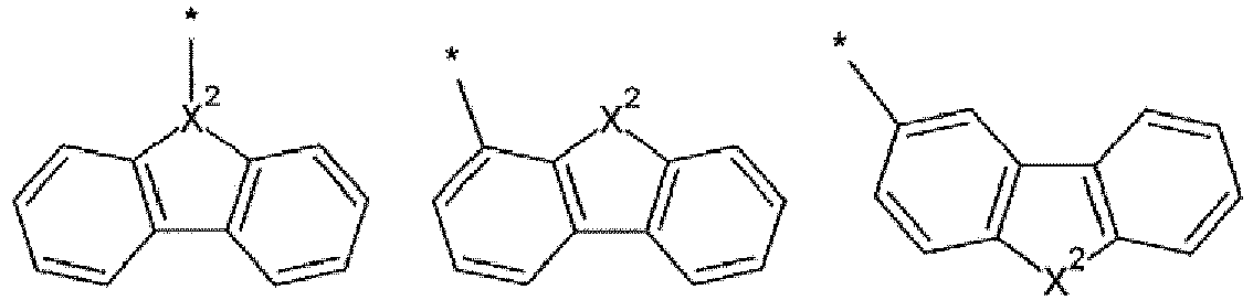 * eine Position angibt, an der sie mit Kohlenstoff (C) verbunden ist,in der chemischen Formel X-4 X2 N ist, undin den chemischen Formeln X-5 und X-6 X2 NR' O oder S ist, wobei R' Wasserstoff, Deuterium, eine substituierte oder unsubstituierte C1- bis C20-Alkylgruppe, eine substituierte oder unsubstituierte C6- bis C30-Arylgruppe oder eine substituierte oder unsubstituierte C2- bis C30-Heteroarylgruppe ist.
 - Verbindung nach Anspruch 7, wobei die substituierte oder unsubstituierte C2- bis C30-Heteroarylgruppe durch die chemische Formel X-7 dargestellt ist:
 * eine Position angibt, an der sie mit Kohlenstoff (C) verbunden ist, undR100 eine substituierte oder unsubstituierte C1- bis C30-Alkylgruppe oder eine substituierte oder unsubstituierte C6 bis C30-Arylgruppe ist.
 - Verbindung nach Anspruch 1, die durch die chemischen Formeln A-51, A-74, A-77, A-94, B-51, B-77, B-94, B-97, C-11, C-15, C-17 oder C-21 dargestellt ist:


- Organisches optoelektronisches Bauelement miteiner Anode und einer Kathode, die einander zugewandt sind; undmindestens einer organischen Dünnschicht, die zwischen der Anode und der Kathode angeordnet ist,wobei die organische Schicht die Verbindung nach einem der Ansprüche 1 bis 11 aufweist.
- Organisches optoelektronisches Bauelement nach Anspruch 12, wobei die organische Schicht eine Emissionsschicht aufweist.
- Organisches optoelektronisches Bauelement nach Anspruch 13, wobei die Verbindung als ein Wirt-Material in der Emissionsschicht enthalten ist.
- Anzeigevorrichtung mit dem organischen optoelektronischen Bauelement nach Anspruch 12.
Applications Claiming Priority (2)
| Application Number | Priority Date | Filing Date | Title |
|---|---|---|---|
| KR1020130081722A KR101627754B1 (ko) | 2013-07-11 | 2013-07-11 | 화합물, 이를 포함하는 유기 광전자 소자 및 표시장치 |
| PCT/KR2013/009896 WO2015005536A1 (ko) | 2013-07-11 | 2013-11-04 | 화합물, 이를 포함하는 유기 광전자 소자 및 표시장치 |
Publications (3)
| Publication Number | Publication Date |
|---|---|
| EP3023425A1 EP3023425A1 (de) | 2016-05-25 |
| EP3023425A4 EP3023425A4 (de) | 2017-03-01 |
| EP3023425B1 true EP3023425B1 (de) | 2019-03-20 |
Family
ID=52280193
Family Applications (1)
| Application Number | Title | Priority Date | Filing Date |
|---|---|---|---|
| EP13889161.9A Active EP3023425B1 (de) | 2013-07-11 | 2013-11-04 | Verbindung, organisches optoelektronisches element damit und anzeigevorrichtung |
Country Status (6)
| Country | Link |
|---|---|
| US (1) | US10141521B2 (de) |
| EP (1) | EP3023425B1 (de) |
| JP (1) | JP6323817B2 (de) |
| KR (1) | KR101627754B1 (de) |
| CN (1) | CN105377844B (de) |
| WO (1) | WO2015005536A1 (de) |
Families Citing this family (6)
| Publication number | Priority date | Publication date | Assignee | Title |
|---|---|---|---|---|
| EP3053985B1 (de) * | 2013-09-30 | 2018-10-31 | LG Chem, Ltd. | Heterocyclische verbindung und organisches lichtemittierendes element damit |
| KR102421581B1 (ko) | 2015-09-08 | 2022-07-18 | 삼성디스플레이 주식회사 | 화합물 및 이를 포함하는 유기 발광 소자 |
| KR102423180B1 (ko) * | 2015-12-18 | 2022-07-21 | 솔루스첨단소재 주식회사 | 유기 화합물 및 이를 포함하는 유기 전계 발광 소자 |
| CN111344289A (zh) * | 2017-12-27 | 2020-06-26 | 广州华睿光电材料有限公司 | 含氮杂环化合物、高聚物、混合物、组合物及其用途 |
| CN110759925A (zh) * | 2018-12-06 | 2020-02-07 | 广州华睿光电材料有限公司 | 含氮稠环有机化合物及其应用 |
| CN114957253A (zh) * | 2022-06-28 | 2022-08-30 | 武汉天马微电子有限公司 | 一种有机化合物、oled器件及其应用 |
Family Cites Families (9)
| Publication number | Priority date | Publication date | Assignee | Title |
|---|---|---|---|---|
| US4549192A (en) * | 1984-07-31 | 1985-10-22 | The Hilton-Davis Chemical Co. | Electrochromic marking systems |
| KR940009187B1 (ko) | 1991-12-13 | 1994-10-01 | 주식회사 금성사 | 마그네트론의 노이즈 저감장치 |
| EP0594538A3 (en) * | 1992-10-20 | 1994-06-29 | Ciba Geigy Ag | Photochromatic acridone derivatives, process for their preparation and their use |
| KR101453872B1 (ko) | 2007-07-24 | 2014-10-23 | 삼성디스플레이 주식회사 | 방향족 화합물 및 이를 포함한 유기막을 구비한 유기 발광소자 |
| WO2009084512A1 (ja) * | 2007-12-28 | 2009-07-09 | Idemitsu Kosan Co., Ltd. | 芳香族アミン誘導体及びそれを用いた有機エレクトロルミネッセンス素子 |
| JP5604804B2 (ja) | 2008-04-25 | 2014-10-15 | 住友化学株式会社 | 含窒素複素環式化合物を含む組成物 |
| KR101120892B1 (ko) | 2009-06-19 | 2012-02-27 | 주식회사 두산 | 아크리딘 유도체 및 이를 포함하는 유기 전계 발광 소자 |
| WO2011074493A1 (ja) * | 2009-12-14 | 2011-06-23 | 凸版印刷株式会社 | アントラセン誘導体および発光素子 |
| KR20110112098A (ko) * | 2010-04-06 | 2011-10-12 | 다우어드밴스드디스플레이머티리얼 유한회사 | 신규한 유기 발광 화합물 및 이를 채용하고 있는 유기 전계 발광 소자 |
-
2013
- 2013-07-11 KR KR1020130081722A patent/KR101627754B1/ko active Active
- 2013-11-04 JP JP2016525260A patent/JP6323817B2/ja active Active
- 2013-11-04 EP EP13889161.9A patent/EP3023425B1/de active Active
- 2013-11-04 US US14/783,499 patent/US10141521B2/en active Active
- 2013-11-04 WO PCT/KR2013/009896 patent/WO2015005536A1/ko not_active Ceased
- 2013-11-04 CN CN201380078156.5A patent/CN105377844B/zh active Active
Non-Patent Citations (1)
| Title |
|---|
| None * |
Also Published As
| Publication number | Publication date |
|---|---|
| US20160056394A1 (en) | 2016-02-25 |
| EP3023425A1 (de) | 2016-05-25 |
| JP6323817B2 (ja) | 2018-05-16 |
| JP2016531096A (ja) | 2016-10-06 |
| WO2015005536A1 (ko) | 2015-01-15 |
| KR101627754B1 (ko) | 2016-06-07 |
| CN105377844A (zh) | 2016-03-02 |
| KR20150007570A (ko) | 2015-01-21 |
| EP3023425A4 (de) | 2017-03-01 |
| CN105377844B (zh) | 2017-09-22 |
| US10141521B2 (en) | 2018-11-27 |
Similar Documents
| Publication | Publication Date | Title |
|---|---|---|
| EP3575296B1 (de) | Triazin verbindung, zusammensetzung und organische opto-elektronische vorrichtung und anzeigevorrichtung | |
| EP2799515B1 (de) | Verbindung für eine organische optoelektronische vorrichtung, organische lichtemittierende diode damit und anzeigevorrichtung mit der organischen lichtemittierenden diode | |
| EP3034581B1 (de) | Zusammensetzung und organisches optoelektronisches element | |
| EP2860783B1 (de) | Organische optoelektrische Vorrichtung und Anzeigevorrichtung | |
| EP3056554B1 (de) | Organische legierung für eine organische optoelektronische vorrichtung, organische optoelektronische vorrichtung und anzeigevorrichtung | |
| EP3015527B1 (de) | Organische verbindung für optoelektrische vorrichtung und zusammensetzung für optoelektrische vorrichtung und organische optoelektrische vorrichtung und anzeigevorrichtung | |
| EP3042943B1 (de) | Zusammensetzung für eine organische optoelektronische vorrichtung, organische optoelektronische vorrichtung und anzeigevorrichtung | |
| EP3312255B1 (de) | Verbindung für eine organische optoelektrische vorrichtung, organische optoelektrische vorrichtung und anzeigevorrichtung | |
| EP3168221B1 (de) | Verbindung, organische optoelektronische diode damit und anzeige | |
| EP2998301A1 (de) | Organische verbindung, organisches optoelektronisches bauelement und anzeigevorrichtung | |
| EP2952511A1 (de) | Organische verbindung, organisches optoelektronisches bauelement und anzeigevorrichtung | |
| EP2719743A2 (de) | Neue verbindungen und diese verwendende organische elektronische vorrichtung | |
| EP2660300A2 (de) | Neue verbindung und organische lichtemittierende vorrichtung damit | |
| EP2889356A2 (de) | Organisches fotoelektrisches element und anzeigevorrichtung damit | |
| EP2476738A2 (de) | Neues heterozyklisches derivat und organische lichtemittierende vorrichtung damit | |
| EP2998300A1 (de) | Organische verbindung, organisches optoelektronisches bauelement und anzeigevorrichtung | |
| EP3006433A1 (de) | Verbindung, organisches lichtemittierendes element damit und anzeigevorrichtung mit dem organischen lichtemittierenden element | |
| EP3345891B1 (de) | Aminverbindung und organische lichtemittierende vorrichtung damit | |
| EP3023425B1 (de) | Verbindung, organisches optoelektronisches element damit und anzeigevorrichtung | |
| CN117551110A (zh) | 有机化合物及使用其的电子元件和电子装置 | |
| CN119841784A (zh) | 新型化合物及包含其的有机发光器件 | |
| KR20150041506A (ko) | 화합물, 이를 포함하는 유기 광전자 소자 및 표시장치 | |
| KR20220107769A (ko) | 화합물 및 이를 포함하는 유기 발광 소자 | |
| KR20240003039A (ko) | 화합물 및 이를 포함하는 유기 발광 소자 | |
| EP2998380A1 (de) | Verbindung für eine organische optoelektronische vorrichtung, organische lichtemittierende diode damit und anzeigevorrichtung mit der organischen lichtemittierenden diode |
Legal Events
| Date | Code | Title | Description |
|---|---|---|---|
| PUAI | Public reference made under article 153(3) epc to a published international application that has entered the european phase |
Free format text: ORIGINAL CODE: 0009012 |
|
| 17P | Request for examination filed |
Effective date: 20151102 |
|
| AK | Designated contracting states |
Kind code of ref document: A1 Designated state(s): AL AT BE BG CH CY CZ DE DK EE ES FI FR GB GR HR HU IE IS IT LI LT LU LV MC MK MT NL NO PL PT RO RS SE SI SK SM TR |
|
| AX | Request for extension of the european patent |
Extension state: BA ME |
|
| DAX | Request for extension of the european patent (deleted) | ||
| A4 | Supplementary search report drawn up and despatched |
Effective date: 20170126 |
|
| RIC1 | Information provided on ipc code assigned before grant |
Ipc: H01L 51/54 20060101ALI20170120BHEP Ipc: C07D 471/04 20060101AFI20170120BHEP Ipc: C09K 11/06 20060101ALI20170120BHEP Ipc: C07D 401/14 20060101ALI20170120BHEP |
|
| REG | Reference to a national code |
Ref country code: DE Ref legal event code: R079 Ref document number: 602013052780 Country of ref document: DE Free format text: PREVIOUS MAIN CLASS: C07D0471040000 Ipc: H01L0051540000 |
|
| GRAP | Despatch of communication of intention to grant a patent |
Free format text: ORIGINAL CODE: EPIDOSNIGR1 |
|
| STAA | Information on the status of an ep patent application or granted ep patent |
Free format text: STATUS: GRANT OF PATENT IS INTENDED |
|
| RIC1 | Information provided on ipc code assigned before grant |
Ipc: C07D 471/04 20060101ALI20181106BHEP Ipc: C09K 11/06 20060101ALI20181106BHEP Ipc: C07D 401/14 20060101ALI20181106BHEP Ipc: H01L 51/54 20060101AFI20181106BHEP |
|
| INTG | Intention to grant announced |
Effective date: 20181205 |
|
| GRAS | Grant fee paid |
Free format text: ORIGINAL CODE: EPIDOSNIGR3 |
|
| GRAA | (expected) grant |
Free format text: ORIGINAL CODE: 0009210 |
|
| STAA | Information on the status of an ep patent application or granted ep patent |
Free format text: STATUS: THE PATENT HAS BEEN GRANTED |
|
| AK | Designated contracting states |
Kind code of ref document: B1 Designated state(s): AL AT BE BG CH CY CZ DE DK EE ES FI FR GB GR HR HU IE IS IT LI LT LU LV MC MK MT NL NO PL PT RO RS SE SI SK SM TR |
|
| REG | Reference to a national code |
Ref country code: GB Ref legal event code: FG4D |
|
| REG | Reference to a national code |
Ref country code: CH Ref legal event code: EP |
|
| REG | Reference to a national code |
Ref country code: DE Ref legal event code: R096 Ref document number: 602013052780 Country of ref document: DE |
|
| REG | Reference to a national code |
Ref country code: AT Ref legal event code: REF Ref document number: 1111412 Country of ref document: AT Kind code of ref document: T Effective date: 20190415 |
|
| REG | Reference to a national code |
Ref country code: IE Ref legal event code: FG4D |
|
| REG | Reference to a national code |
Ref country code: NL Ref legal event code: MP Effective date: 20190320 |
|
| PG25 | Lapsed in a contracting state [announced via postgrant information from national office to epo] |
Ref country code: SE Free format text: LAPSE BECAUSE OF FAILURE TO SUBMIT A TRANSLATION OF THE DESCRIPTION OR TO PAY THE FEE WITHIN THE PRESCRIBED TIME-LIMIT Effective date: 20190320 Ref country code: NO Free format text: LAPSE BECAUSE OF FAILURE TO SUBMIT A TRANSLATION OF THE DESCRIPTION OR TO PAY THE FEE WITHIN THE PRESCRIBED TIME-LIMIT Effective date: 20190620 Ref country code: FI Free format text: LAPSE BECAUSE OF FAILURE TO SUBMIT A TRANSLATION OF THE DESCRIPTION OR TO PAY THE FEE WITHIN THE PRESCRIBED TIME-LIMIT Effective date: 20190320 Ref country code: LT Free format text: LAPSE BECAUSE OF FAILURE TO SUBMIT A TRANSLATION OF THE DESCRIPTION OR TO PAY THE FEE WITHIN THE PRESCRIBED TIME-LIMIT Effective date: 20190320 |
|
| REG | Reference to a national code |
Ref country code: LT Ref legal event code: MG4D |
|
| PG25 | Lapsed in a contracting state [announced via postgrant information from national office to epo] |
Ref country code: BG Free format text: LAPSE BECAUSE OF FAILURE TO SUBMIT A TRANSLATION OF THE DESCRIPTION OR TO PAY THE FEE WITHIN THE PRESCRIBED TIME-LIMIT Effective date: 20190620 Ref country code: GR Free format text: LAPSE BECAUSE OF FAILURE TO SUBMIT A TRANSLATION OF THE DESCRIPTION OR TO PAY THE FEE WITHIN THE PRESCRIBED TIME-LIMIT Effective date: 20190621 Ref country code: HR Free format text: LAPSE BECAUSE OF FAILURE TO SUBMIT A TRANSLATION OF THE DESCRIPTION OR TO PAY THE FEE WITHIN THE PRESCRIBED TIME-LIMIT Effective date: 20190320 Ref country code: NL Free format text: LAPSE BECAUSE OF FAILURE TO SUBMIT A TRANSLATION OF THE DESCRIPTION OR TO PAY THE FEE WITHIN THE PRESCRIBED TIME-LIMIT Effective date: 20190320 Ref country code: LV Free format text: LAPSE BECAUSE OF FAILURE TO SUBMIT A TRANSLATION OF THE DESCRIPTION OR TO PAY THE FEE WITHIN THE PRESCRIBED TIME-LIMIT Effective date: 20190320 Ref country code: RS Free format text: LAPSE BECAUSE OF FAILURE TO SUBMIT A TRANSLATION OF THE DESCRIPTION OR TO PAY THE FEE WITHIN THE PRESCRIBED TIME-LIMIT Effective date: 20190320 |
|
| REG | Reference to a national code |
Ref country code: AT Ref legal event code: MK05 Ref document number: 1111412 Country of ref document: AT Kind code of ref document: T Effective date: 20190320 |
|
| PG25 | Lapsed in a contracting state [announced via postgrant information from national office to epo] |
Ref country code: IT Free format text: LAPSE BECAUSE OF FAILURE TO SUBMIT A TRANSLATION OF THE DESCRIPTION OR TO PAY THE FEE WITHIN THE PRESCRIBED TIME-LIMIT Effective date: 20190320 Ref country code: ES Free format text: LAPSE BECAUSE OF FAILURE TO SUBMIT A TRANSLATION OF THE DESCRIPTION OR TO PAY THE FEE WITHIN THE PRESCRIBED TIME-LIMIT Effective date: 20190320 Ref country code: RO Free format text: LAPSE BECAUSE OF FAILURE TO SUBMIT A TRANSLATION OF THE DESCRIPTION OR TO PAY THE FEE WITHIN THE PRESCRIBED TIME-LIMIT Effective date: 20190320 Ref country code: CZ Free format text: LAPSE BECAUSE OF FAILURE TO SUBMIT A TRANSLATION OF THE DESCRIPTION OR TO PAY THE FEE WITHIN THE PRESCRIBED TIME-LIMIT Effective date: 20190320 Ref country code: EE Free format text: LAPSE BECAUSE OF FAILURE TO SUBMIT A TRANSLATION OF THE DESCRIPTION OR TO PAY THE FEE WITHIN THE PRESCRIBED TIME-LIMIT Effective date: 20190320 Ref country code: PT Free format text: LAPSE BECAUSE OF FAILURE TO SUBMIT A TRANSLATION OF THE DESCRIPTION OR TO PAY THE FEE WITHIN THE PRESCRIBED TIME-LIMIT Effective date: 20190720 Ref country code: SK Free format text: LAPSE BECAUSE OF FAILURE TO SUBMIT A TRANSLATION OF THE DESCRIPTION OR TO PAY THE FEE WITHIN THE PRESCRIBED TIME-LIMIT Effective date: 20190320 Ref country code: AL Free format text: LAPSE BECAUSE OF FAILURE TO SUBMIT A TRANSLATION OF THE DESCRIPTION OR TO PAY THE FEE WITHIN THE PRESCRIBED TIME-LIMIT Effective date: 20190320 |
|
| PG25 | Lapsed in a contracting state [announced via postgrant information from national office to epo] |
Ref country code: PL Free format text: LAPSE BECAUSE OF FAILURE TO SUBMIT A TRANSLATION OF THE DESCRIPTION OR TO PAY THE FEE WITHIN THE PRESCRIBED TIME-LIMIT Effective date: 20190320 Ref country code: SM Free format text: LAPSE BECAUSE OF FAILURE TO SUBMIT A TRANSLATION OF THE DESCRIPTION OR TO PAY THE FEE WITHIN THE PRESCRIBED TIME-LIMIT Effective date: 20190320 |
|
| PG25 | Lapsed in a contracting state [announced via postgrant information from national office to epo] |
Ref country code: AT Free format text: LAPSE BECAUSE OF FAILURE TO SUBMIT A TRANSLATION OF THE DESCRIPTION OR TO PAY THE FEE WITHIN THE PRESCRIBED TIME-LIMIT Effective date: 20190320 Ref country code: IS Free format text: LAPSE BECAUSE OF FAILURE TO SUBMIT A TRANSLATION OF THE DESCRIPTION OR TO PAY THE FEE WITHIN THE PRESCRIBED TIME-LIMIT Effective date: 20190720 |
|
| REG | Reference to a national code |
Ref country code: DE Ref legal event code: R097 Ref document number: 602013052780 Country of ref document: DE |
|
| PLBE | No opposition filed within time limit |
Free format text: ORIGINAL CODE: 0009261 |
|
| STAA | Information on the status of an ep patent application or granted ep patent |
Free format text: STATUS: NO OPPOSITION FILED WITHIN TIME LIMIT |
|
| PG25 | Lapsed in a contracting state [announced via postgrant information from national office to epo] |
Ref country code: DK Free format text: LAPSE BECAUSE OF FAILURE TO SUBMIT A TRANSLATION OF THE DESCRIPTION OR TO PAY THE FEE WITHIN THE PRESCRIBED TIME-LIMIT Effective date: 20190320 |
|
| 26N | No opposition filed |
Effective date: 20200102 |
|
| PG25 | Lapsed in a contracting state [announced via postgrant information from national office to epo] |
Ref country code: SI Free format text: LAPSE BECAUSE OF FAILURE TO SUBMIT A TRANSLATION OF THE DESCRIPTION OR TO PAY THE FEE WITHIN THE PRESCRIBED TIME-LIMIT Effective date: 20190320 |
|
| PG25 | Lapsed in a contracting state [announced via postgrant information from national office to epo] |
Ref country code: TR Free format text: LAPSE BECAUSE OF FAILURE TO SUBMIT A TRANSLATION OF THE DESCRIPTION OR TO PAY THE FEE WITHIN THE PRESCRIBED TIME-LIMIT Effective date: 20190320 |
|
| REG | Reference to a national code |
Ref country code: CH Ref legal event code: PL |
|
| PG25 | Lapsed in a contracting state [announced via postgrant information from national office to epo] |
Ref country code: LU Free format text: LAPSE BECAUSE OF NON-PAYMENT OF DUE FEES Effective date: 20191104 Ref country code: CH Free format text: LAPSE BECAUSE OF NON-PAYMENT OF DUE FEES Effective date: 20191130 Ref country code: MC Free format text: LAPSE BECAUSE OF FAILURE TO SUBMIT A TRANSLATION OF THE DESCRIPTION OR TO PAY THE FEE WITHIN THE PRESCRIBED TIME-LIMIT Effective date: 20190320 Ref country code: LI Free format text: LAPSE BECAUSE OF NON-PAYMENT OF DUE FEES Effective date: 20191130 |
|
| REG | Reference to a national code |
Ref country code: BE Ref legal event code: MM Effective date: 20191130 |
|
| GBPC | Gb: european patent ceased through non-payment of renewal fee |
Effective date: 20191104 |
|
| PG25 | Lapsed in a contracting state [announced via postgrant information from national office to epo] |
Ref country code: IE Free format text: LAPSE BECAUSE OF NON-PAYMENT OF DUE FEES Effective date: 20191104 Ref country code: FR Free format text: LAPSE BECAUSE OF NON-PAYMENT OF DUE FEES Effective date: 20191130 Ref country code: GB Free format text: LAPSE BECAUSE OF NON-PAYMENT OF DUE FEES Effective date: 20191104 |
|
| PG25 | Lapsed in a contracting state [announced via postgrant information from national office to epo] |
Ref country code: BE Free format text: LAPSE BECAUSE OF NON-PAYMENT OF DUE FEES Effective date: 20191130 |
|
| PG25 | Lapsed in a contracting state [announced via postgrant information from national office to epo] |
Ref country code: CY Free format text: LAPSE BECAUSE OF FAILURE TO SUBMIT A TRANSLATION OF THE DESCRIPTION OR TO PAY THE FEE WITHIN THE PRESCRIBED TIME-LIMIT Effective date: 20190320 |
|
| PG25 | Lapsed in a contracting state [announced via postgrant information from national office to epo] |
Ref country code: HU Free format text: LAPSE BECAUSE OF FAILURE TO SUBMIT A TRANSLATION OF THE DESCRIPTION OR TO PAY THE FEE WITHIN THE PRESCRIBED TIME-LIMIT; INVALID AB INITIO Effective date: 20131104 Ref country code: MT Free format text: LAPSE BECAUSE OF FAILURE TO SUBMIT A TRANSLATION OF THE DESCRIPTION OR TO PAY THE FEE WITHIN THE PRESCRIBED TIME-LIMIT Effective date: 20190320 |
|
| PG25 | Lapsed in a contracting state [announced via postgrant information from national office to epo] |
Ref country code: MK Free format text: LAPSE BECAUSE OF FAILURE TO SUBMIT A TRANSLATION OF THE DESCRIPTION OR TO PAY THE FEE WITHIN THE PRESCRIBED TIME-LIMIT Effective date: 20190320 |
|
| REG | Reference to a national code |
Ref country code: DE Ref legal event code: R079 Ref document number: 602013052780 Country of ref document: DE Free format text: PREVIOUS MAIN CLASS: H01L0051540000 Ipc: H10K0085000000 |
|
| P01 | Opt-out of the competence of the unified patent court (upc) registered |
Effective date: 20230528 |
|
| PGFP | Annual fee paid to national office [announced via postgrant information from national office to epo] |
Ref country code: DE Payment date: 20251104 Year of fee payment: 13 |