EP3026599A1 - Verfahren zur Herstellung von elektronischen Vorrichtungen mit Personalisierungsinformation - Google Patents
Verfahren zur Herstellung von elektronischen Vorrichtungen mit Personalisierungsinformation Download PDFInfo
- Publication number
- EP3026599A1 EP3026599A1 EP14306914.4A EP14306914A EP3026599A1 EP 3026599 A1 EP3026599 A1 EP 3026599A1 EP 14306914 A EP14306914 A EP 14306914A EP 3026599 A1 EP3026599 A1 EP 3026599A1
- Authority
- EP
- European Patent Office
- Prior art keywords
- support
- electronic device
- electronic
- manufacturing
- separable
- Prior art date
- Legal status (The legal status is an assumption and is not a legal conclusion. Google has not performed a legal analysis and makes no representation as to the accuracy of the status listed.)
- Withdrawn
Links
Images


Classifications
-
- G—PHYSICS
- G06—COMPUTING OR CALCULATING; COUNTING
- G06K—GRAPHICAL DATA READING; PRESENTATION OF DATA; RECORD CARRIERS; HANDLING RECORD CARRIERS
- G06K19/00—Record carriers for use with machines and with at least a part designed to carry digital markings
- G06K19/06—Record carriers for use with machines and with at least a part designed to carry digital markings characterised by the kind of the digital marking, e.g. shape, nature, code
- G06K19/067—Record carriers with conductive marks, printed circuits or semiconductor circuit elements, e.g. credit or identity cards also with resonating or responding marks without active components
- G06K19/07—Record carriers with conductive marks, printed circuits or semiconductor circuit elements, e.g. credit or identity cards also with resonating or responding marks without active components with integrated circuit chips
- G06K19/077—Constructional details, e.g. mounting of circuits in the carrier
- G06K19/07716—Constructional details, e.g. mounting of circuits in the carrier the record carrier comprising means for customization, e.g. being arranged for personalization in batch
-
- G—PHYSICS
- G06—COMPUTING OR CALCULATING; COUNTING
- G06K—GRAPHICAL DATA READING; PRESENTATION OF DATA; RECORD CARRIERS; HANDLING RECORD CARRIERS
- G06K19/00—Record carriers for use with machines and with at least a part designed to carry digital markings
- G06K19/06—Record carriers for use with machines and with at least a part designed to carry digital markings characterised by the kind of the digital marking, e.g. shape, nature, code
- G06K19/067—Record carriers with conductive marks, printed circuits or semiconductor circuit elements, e.g. credit or identity cards also with resonating or responding marks without active components
- G06K19/07—Record carriers with conductive marks, printed circuits or semiconductor circuit elements, e.g. credit or identity cards also with resonating or responding marks without active components with integrated circuit chips
- G06K19/077—Constructional details, e.g. mounting of circuits in the carrier
- G06K19/07718—Constructional details, e.g. mounting of circuits in the carrier the record carrier being manufactured in a continuous process, e.g. using endless rolls
-
- G—PHYSICS
- G06—COMPUTING OR CALCULATING; COUNTING
- G06K—GRAPHICAL DATA READING; PRESENTATION OF DATA; RECORD CARRIERS; HANDLING RECORD CARRIERS
- G06K19/00—Record carriers for use with machines and with at least a part designed to carry digital markings
- G06K19/06—Record carriers for use with machines and with at least a part designed to carry digital markings characterised by the kind of the digital marking, e.g. shape, nature, code
- G06K19/067—Record carriers with conductive marks, printed circuits or semiconductor circuit elements, e.g. credit or identity cards also with resonating or responding marks without active components
- G06K19/07—Record carriers with conductive marks, printed circuits or semiconductor circuit elements, e.g. credit or identity cards also with resonating or responding marks without active components with integrated circuit chips
- G06K19/077—Constructional details, e.g. mounting of circuits in the carrier
- G06K19/07743—External electrical contacts
Definitions
- the invention relates to a method of manufacturing a portable electronic device comprising a support, an electronic object separable from the support and personalization information on the support as well as the electronic device obtained and the support in the separated state.
- the invention further relates to a packaging tape of a plurality of electronic devices thus manufactured.
- Such devices or electronic objects targeted by the invention may be found, for example in the form of cards with various form factors such as those of small electronic objects of micro-SD ( Secure Digital ) formats, Micro -SIM (acronym for " Subscriber Identity Module ”) or Plug-in SIM, Mini UICC (acronym for " Universal Integrated Circuit Card “).
- a whole range of electronic objects can be found in the form of housings, allowing the mounting of surface components (noted CMS in French or SMD in English for "Surface Mounted Device”), as well as BGA-type enclosures. (acronym for "Ball Grid Array”) with connecting balls.
- These boxes include a power supply and / or communication interface including electrical contacts or antenna.
- the invention relates more particularly, but in a non-limiting manner, to the manufacture of secure portable electronic devices or objects such as smart cards or modules which find particular applications in health, banking, telecommunications or even identity control. , physical and / or logical access control.
- SIM card As prior art and closest electronic device, we know the SIM card described in particular in the EP0521778 .
- This SIM card includes a card body in ISO 7816 standard format (credit card format) and a mini-SIM card (mini-SIM) in a reduced format compared to this standard format.
- This mini-SIM is delimited by a precut in the ISO 7816 standard card body and is connected to the card body by manually breakable straps.
- the mini-SIM card comprises an electronic module housed in a cavity formed on the surface of the mini-card and / or SIM card (a chip card module comprises a microcircuit carried by a dielectric support film, the microcircuit being coated with a protective material and being connected to an interface with electrical contacts flush with the surface of the mini-card body).
- the mini SIM card is formed in the body of the ISO 7816 format card and has the same thickness.
- the surface of the SIM card body (or even mini-SIM card) also includes any graphic printing such as a distributor logo or mobile operator
- the patent application WO2014044684 describes a method of manufacturing housings or electronic objects on a support.
- Metallization sets are made on the support with optimized maximum density, then an electronic chip is transferred and connected to each set of metallizations, each chip is overmolded with a molding material to make a housing so that the metallizations are transferred into the overmoulding material at the time of separation of the removable housing.
- the housings are then separated from the removed media which is during the separation of the housing or later.
- the support has a low or alterable adhesiveness and overmoulding is performed at the final size of the housing.
- the document EP1 780 662 describes the possibility of coating the chip and its connections in a mold in which a reinforcing pad is disposed prior to the step of molding the coating resin. Such a reinforcing pad makes it possible to mechanically protect the electronic module.
- the electronic module thus produced is then embedded in the body of a housing to form an electronic device. For this, the module is carried in a cavity formed in the body of the housing.
- the document FR2 833 736 further described a method of overmoulding a housing on a removable paper support. Once the molded case, a subsequent step is to machine a cavity in the housing to carry an electronic module and thus obtain a smart card. The smart card thus obtained is then separated from its removable paper support.
- the nano-SIM card still noted under the acronym 4FF, whose thickness is normalized to 0.67mm, must have a reduced thickness of 11% compared to the micro-SIM card, noted under the acronym 3FF. Therefore, it also becomes important to find solutions to optimize manufacturing processes, to take into account these requirements and allow the obtaining of electronic devices of reduced thickness and size.
- the invention therefore aims to remedy at least one of the disadvantages of the prior art.
- the invention aims to reduce costs by integrating or facilitating as much as possible the operations generally used in the manufacture and distribution of electronic devices, including that of providing personalization information on the devices.
- the principle of the invention is based on the creation of a personalization zone for receiving information, in particular graphics, on the same support or dielectric support film usually intended to produce and convey smart card modules; this metallized support or dielectric film metallized with the interface is generally called "lead frame" in English terminology.
- the information generally provided on the outer surface of a smart card body is now made thanks to the invention at the level of the metallized support film itself.
- the latter has so far never been used or planned for this function.
- the metallized support coils present for practical and cost-effective issues, a density of module location as large as possible without leaving a lost space.
- the grid is generally etched, those skilled in the art seek to minimize the metal (copper) lost during etching and thus to optimize the location of the modules.
- the dielectric support film for smart card modules is very expensive (or even more expensive than the metallizations) and it is necessary to optimize their surface with a maximum of module locations per unit area.
- the invention firstly requires reducing the density of module locations on the metallized support (metallized dielectric film) thus counter-current to the natural tendency of productivity of the person skilled in the art or the needs of the art. 'industry.
- the invention then requires devoting space thus created to provide personalization information or graphic printing.
- a lower quality is used for the dielectric backing film with a compromise as to the tensile strength for the post-to-post workout.
- the personalization information can be provided directly continuously on the support or metallized dielectric coil presented with an optimized performance of customization.
- the manufacturing method is very simple and allows to remove a number of conventional steps in the manufacture of smart cards.
- the injection steps of the card body or molding, as well as the steps of cutting and insertion of the electronic module into a cavity of the card body are no longer necessary.
- a personalization information input is provided on the metallized support of the electronic object.
- the method also makes it possible to obtain objects of reduced thickness.
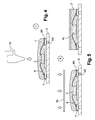
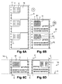
- the Figures 1 to 6B describe the steps of an embodiment of the method of manufacturing a portable electronic device 1A comprising a support 5 and an electronic object b1 separable from each other; According to this mode, the method comprises a step of providing personalization information in a reserved space of the support.
- the support of the portable electronic object receives or is intended to receive personalization information.
- the method reproduces a printing step substantially as in the manufacture of smart cards where printing is performed on the card body around a mini-chip card detachable from the body of map.
- the first step of producing at least one electrically conductive metallization (or set of metallizations) on the separable support is described in particular in connection with the Figures 1 to 5 below.
- the second step is described later.
- the metallization may comprise a continuous conductive element such as an antenna or electrical contact pads, or tracks, or connection or solder tabs of any electronic component of the CMS type.
- the Figure 1 illustrates the various steps 1 to 5 for producing at least one set of metallizations 4 comprising copper contacts on a removable substrate 5, that is to say a detachable or separable substrate of the electronic object.
- Substrate 5, also called support in the following description is a dielectric film chosen for its low adhesion properties (low cost compared to the dielectric generally used in the chip card industry), so that the resin or protective material subsequently dispensed to its surface is easily detached.
- the material of constitution of such a support may for example be chosen from polymers such as PET (polyethylene terephthalate), PEN (polyethylene naphthalate), or a cheap material of the synthetic or natural paper type.
- the dielectric support film generally used for chip card modules is a composite formed of glass fibers in an epoxy matrix, or also in polyimide (commonly known as Kapton), ...
- an antenna In the case of an antenna, it can be made flat as a spiral.
- the description is made preferentially for metallizations with electrical contacts, but the invention can also be applied to other electrically conductive elements such as plates, tracks or antennas, for example.
- the contact interface 4 can be replaced by an antenna radio frequency interface.
- the medium 5 is determined with a plurality of locations each for receiving an electronic object body.
- Each location therefore also includes an area reserved for information contrary to the prior art.
- this information area is distinct from the location of the electronic object body;
- there may be overlap or printing in the same area as the location of the device body, for example around or between the metallizations M2.
- lead or solder tabs may extend beyond the location of the component body.
- the surface metallizations are carried out by means of a process involving current feed tracks (especially for electrolytic deposition), care will be taken that these tracks are few in number and have a facilitating configuration. their separation, during the separation of the electronic devices obtained and the low-tack support, for example by having a form of necking, or precut or reduction of section where they must be cut. Also, these can be removed by etching or cut locally by laser or any other equivalent method.
- a first step 1 therefore consists in providing a dielectric support film 5, preferably coated with a low tack adhesive and thus forming the removable support 5.
- the adhesive may be slightly adherent by nature or heat-degradable or degradable with UV (ultraviolet) or degradable with IR (infrared), so that each metallization or set of metallizations 4, especially copper, and the protective resin 7 subsequently deposited on its surface, detach easily.
- the low tack values for the metallizations 4 and the protective resin 7 to be able to separate from the support 5 can typically be between 0.5 and 5 Newton / cm in the 90 degree peel strength test.
- the peel rate may be, for example, 30 cm / minute or more.
- the support 5 is then drilled, in particular by punching, as illustrated in step 2.
- the holes T obtained will subsequently make it possible to perform a surface treatment of the metallizations 4 (titanium, gold, silver, palladium, nickel, etc.) . These holes also facilitate the separation of the removable support 5 and the electronic device obtained since the metallizations adhere only to a frame or thin rim around the openings or holes obtained by punching.
- step 3 a temporary fixing is carried out, in particular by lamination with or without an intermediate adhesive, of an electrically conductive sheet 3, in particular made of copper, on the removable dielectric support 5.
- the next step 4 is then to perform a chemical etching of the conductive sheet 3 to achieve the desired shape of the external contacts 4 for the electronic device in manufacture.
- a surface treatment M1, M2 of the copper parts is preferably carried out.
- This treatment of metallizations 4 consists in adding a additional metallization layer, Ni / Pd / Au type (nickel / palladium / gold) for example, forming a passivation layer M1 and / or M2 on the contacts 4.
- This treatment can be done on both sides of the sheet of engraved copper.
- the face in contact with the removable support 5 can in fact also be surface-treated through the holes T previously drilled in the removable support 5.
- the external contacts 4 intended to be substantially flush with the external surface of the electronic device, to the thickness of the treatment layer M2 near or the adhesive layer of the removable support 5, are also processed.
- the removable support 5 above may be unpunched, as illustrated in FIG. Figure 2 .
- the external contacts 4 can remain in copper and possibly be protected from oxidation by organic passivation or other surface treatment before or after.
- the above substrate can be punched, as illustrated in FIG. Figure 1 , a number of holes T greater than those necessary for the metallization treatment M2 of the contacts 4, this in order to improve the subsequent separation between the removable support 5 and the electronic device obtained, the surface facing each other being indeed weaker.
- the contact pads 4 may be perforated to limit adhesion and to save metallizations and / or to allow electromagnetic permeability in the case where the object also comprises a radiofrequency antenna, for example etched on the support.
- an antenna (not shown) is produced, for example at the same level as the conductive contacts or tracks, especially at the periphery and / or in a central zone with respect to the contact pads 4.
- an electrically conductive grid in particular by a jet of conductive material, on the removable support 5 to form electrical contacts 4 and / or tracks and / or at least one antenna.
- an integrated circuit electronic chip 2 is carried on the face 9 of the removable support 5 comprising the metallizations 4. It can also be transferred directly to these conductive elements (tracks, tracks, turns antenna).
- the chip 2 is then connected to the metal contacts 4 by wire connection 8 for example.
- a cleaning plasma may optionally be used to improve the adhesion of the resin or protective material 7, subsequently dispensed, to the metallized contacts 4.
- the electrical connection of the chip 2 of the integrated circuit with the contacts 4 can also be performed by the known technique of "flip chip", or flipped chip.
- step 7 the dispensing of a resin or insulating protective material 7 is carried out to coat the chip and its connections 8 (wires), by means of a dispensing device 15 conventionally used in the field of the smart card.
- an adhesion of the metallizations 4 is provided which is greater in contact with the protective resin 7 than in contact with the removable support 5.
- This adhesion can also be improved by various known methods, such as, for example, by increasing the roughness of the copper of the contacts 4, by increasing the surface roughness (the additional metallization M1, M2, Ni / Pd / Au then follows this roughness), by cleaning plasma before dispensing the protective resin, by anchoring points of the protective resin in conductive portions of the metallizations.
- a cut-off pad 10 may be deferred to the final size of the device.
- This pellet has in particular a surface delimiting the final contour of the electronic device.
- the pellet is transferred to the protective resin 7 while the latter is not cured.
- This reinforcing pad 10 not only makes it possible to stiffen and mechanically protect the electronic device, but also to obtain a geometrically homogeneous electronic device, in particular by presenting a flat surface.
- This reinforcing pad is advantageously packaged in roll and is cut to the final size of the device.
- the pellet 10 may also be formed in series, for example by molding, and packaged on weakly adhesive removable media.
- the pellet is placed on the protective resin by means of automatic transfer equipment conventionally used in card manufacturing processes.
- This pellet may, for example, have a decoration, made by printing, by pad printing or any other equivalent method, on its flat surface intended to form an external surface opposite to that supporting the metal contacts 4.
- the surface supporting the metal contacts 4 is itself even formed by the protective resin 7.
- the pellet 10 is positioned on the top of the connection wires 8. Under the action of the weight of the pellet 10, the protective resin 7 is distributed by capillarity up to the contours of the device to form its lateral edges and give it its thickness. final.
- the nature of the pellet may be a composite such as an epoxy glass or a thermoplastic polymer such as PET (polyethylene terephthalate), PEN (polyethylene naphthalate), PC (polycarbonate), etc.
- the typical thickness of the pellet can vary from 50 ⁇ m to 300 ⁇ m depending on its material, the space that we want to leave the chip and its connections and the desired thickness of the final electronic device.
- the resin or protective material may be a heat curing resin or a UV curing resin.
- the resin is cured by exposure to UV radiation.
- Such a resin has indeed interesting advantages. In particular, because of the low thermal input of such a polymerization, inexpensive and poorly temperature-resistant removable supports can be used. In addition the electronic device is not likely to be deformed due to too large differential expansions between the different materials. Finally, the UV irradiation can be carried out through the wafer 10, when its constituent material is chosen to pass the UV wavelengths, as through the removable support 5 when it is made of a UV-transparent material. .
- the thickness of the resin varies according to the thickness of the final object to be produced and according to the thickness of the reinforcing pad.
- the thickness of the resin between the inner surface of the reinforcing pad 10 and the inner surface of the support removable 5 will be between 300 and 600 ⁇ m.
- the removable dielectric support 5 is heated to a moderate temperature, that is to say at a temperature below the polymerization temperature of the resin 7, when the latter is heat-polymerizable, at thin the latter and promote its distribution to the contour of the electronic device.
- the pellet can be colored, or tinted in the mass.
- the protective resin 7 is transparent, the face around the contacts 4 appears colored.
- a stop means capable of preventing creep of the protective resin 7 and the appearance of burrs on the final device.
- This stop means extends along the contour of the final device and is arranged on the removable support 5 and / or on the contour of the reinforcing pad 10.
- Such a stop means has the function of stopping creep of the protective resin, in order to give the final electronic device perfectly straight edges at the moment of detachment of the removable support 5.
- this stop means can be achieved either by metal etching of the contour, or by adding material.
- metal etching for example, it may advantageously be in the form of a metal contour engraved in the metal sheet 3, provisionally fixed on the removable support 5, simultaneously with the production of the contacts 4 of the future device. electronic on the removable support.
- Such an engraved metal contour is represented on the Figure 6A under the reference 11.
- the metal contour is made to a width sufficient for the metal of constitution adheres more to the removable medium 5 that the end of protective resin bead possibly flowing on its surface.
- the metal contour 11 and the end resin bead possibly flowing on its surface do not delaminate at the same time as the contacts 4 and always adhere to the removable support 5.
- the metal contour 11 can also be hooked by many current leads that hold it. Also, still for the same purpose, this metal contour 11 can be extended over a large part of the removable support 5 see up to its edge. It can also be retained by plating a piece against the contour at the moment of detachment of the removable support.
- this metal contour 11 may be large in area, it will preferably be metallized by the "spot plating" technique of electrolytic deposition in localized areas of reduced and preferential surfaces. (selectivity process) Such a metal deposit reduces the amount of metal used and avoid the use of precious metal such as gold.
- the metal contour may for example be made of copper-nickel.
- the stop means may for example be made by adding material. This contribution of material may be made on the contour of the face of the wafer 10 intended to rest on the protective resin 7, or on the removable support along the final contour of the device.
- This material supply can be achieved by printing material or by dispensing an elastomeric material such as a silicone for example. It thus forms a rim or an extra thickness.
- the stop means can also be an integral part of the wafer 10 when this is done by a molding technique for example.
- the realization of the body of the object can be performed by overmoulding directly to the final format of the object.
- the height of the stop means, or flange is equal to all or part of the final thickness of the device.
- the invention provides to use the space (or zone) reserved personalization 15 to advantageously perform a graphic printing 16 including the logo of a company and / or to add information specific to the portable object or any information.
- the information may include a PUK unlock code or PIN identification code.
- the information may include a bank code or any other identifier or code.
- the input of information, in particular graphics, can be made at any time during the manufacture of the electronic device or the object, in particular before or after the metallizations are made, before or after the connection of a microcircuit to the interface, the realization of the body of the object or a step of electrical customization of the object.
- the printing can include a printing technique by inkjet, offset, screen printing ...
- the reserved space can be used to print a means allowing a subsequent reading such as a barcode or a 3D code, a photo. It can be used to carry a radio frequency transponder including RFID type (RF, UHF ...) associated with each portable object.
- the RFID antenna can be made at the same time as the metallizations.
- the graphic customization is performed after assembly and connection of the microcircuit of the object.
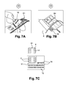
- the resulting electronic object B1 whose contacts 4 adhering to the protective resin 7, is separated from the removable support 5. This separation can be carried out in different ways.
- the carrier film 5 is determined with a plurality of electronic device receiving areas 1A or objects B1 for producing a plurality of devices or objects in series, which are packaged on the removable medium 5;
- This support film can itself be wound for example.
- the electronic object B1 is detached and there remains on the support 5 only the holes T previously punched on the support 5 and the stop means 11 of the resin possibly formed along the periphery device 1 exterior and the personalization information.
- the adhesive may be a thermoplastic or thermo-fusible adhesive.
- destruction of the support may be carried out, particularly by burning, as in the case of a paper support for example. It is also possible to separate the individual objects B1 by peeling the substrate 5. The objects B1 being held by suction on the nozzles 21.
- the electronic objects 1A to 1C obtained here comprise the shape of mini cards 1A, 1B, 1C with electrical contacts 4 flush with their main surface.
- the protective resin 7, constituting the insulating body of the mini-card, comprises a face 3 which can lie at the same level as the contact pads 4.
- the different metallizations 4 are spaced apart from insulating material, ie -desire of the protective resin 7, and substantially flush the outer face 3 of the device formed by the protective resin 7.
- the metallization layer M2 of the surface treatment located in the hole T of the removable support 5, to distinguish from the metallization 4 the support may have a higher level at the outer face 3 of the protective resin 7.
- the contact pads 4 of the device 1 can af bloom the main surface 3 of the protective resin 7, a value between 0 .mu.m and preferably 25 .mu.m or 50 .mu.m.
- the object 1A may comprise, in the center, a zone 40 for any metallization (contact, antenna ).
- the object 1B is parallelepipedic and the object 1C includes a polarizer 41 in addition to the previous one.
- the invention it is possible to arrange electrical / electronic components or metallizations 4 of the electronic device, before the coating step, so that the external surface of the components is at the same level, or substantially at the same level, as the outer surface 3 of the protective resin 7 dispensed at the time of the coating step.
- the thickness of the electronic devices can thus be reduced as much as possible.
- the chip may be placed directly on one of the metallizations 4 or directly on the removable support 5.
- the number of superposed elements and constituting the electronic device is reduced.
- the electronic devices made according to the invention no longer include a dielectric support film in their final constitution.
- the process steps are less numerous, the overmolding steps of a device body being in particular suppressed.
- the transfer of the pellet 10 to the final format of the electronic device, on the protective resin 7, allows for a single step encapsulation of the chip and its connections, and the realization of the body of the final electronic device.
- the chip in another variant, concerning the attachment of the chip, it can be glued directly on the face 9 of the removable medium 5 of low tack, unlike the Figure 3 .
- the adhesive for fixing the chip is at the same level as the external face 3 of the protective resin 7 of the electronic device 1, or substantially at the same level as the metallizations 4.
- the rear face of the chip 2 is found on the surface 3 of the electronic device 1.
- an electronic component such as a fingerprint sensor may come to the surface of the face 3 of the electronic device as mounted as the chip 2, directly against the surface 9 of the removable support 5.
- a component such as a chip or element performing a fingerprint sensor function, can be mounted to provide a flat surface flush with the outer surface 3 of the electronic device.
- This invention also makes it possible to reduce the thickness of the SIM cards if necessary because, only the useful contacts or metallizations are preserved, after transfers of these in the protective resin and separation of the thickness of removable support.
- the contacts are integrated in the protective resin and have very little or no excess thickness.
- the method of manufacturing the electronic devices according to the invention has a reduced number of steps, which results in a reduction in terms of costs.
- the ribbon comprising the electronic devices can be pre-cut or cut by laser or punching.
- the perforated edge can be removed to leave only the electronic devices isolated from each other.
- Electronic devices can be presented by being attached to an additional adhesive or removable tape while in a separate or pre-cut state of the other devices.
- the additional ribbon can be of color determined (white, black ...) and include a customization visible through the support 5. This customization can be carried out by laser through the transparency of the support 5 or directly on the support thus improving the contrast.
- the first support 5 can be attached to a second ribbon or second support to strengthen it, give it more strength, thickness or constituting a contrast medium according to the needs of the customer or user.
- This second support can be deposited on one of the faces of the first support film.
- it can be deposited on the side of the object so as to make a thickness compensation.
- the object is contained in a cavity or recess of the second support.
- the body of the object may at the limit be sealed in a recess or cavity of the second support and in contact with the wall of the cavity without exceeding the height of the cavity.
- metallization 3 may persist on at least the information area.
- the metallization of this zone makes it possible to strengthen the support film and to have a better surface state or contrast of graphic printing or other marking (in particular laser, inkjet, etc.).
- the body of the device may be a metallized film on the entire surface of the support.
- the metallized layer may extend continuously or be isolated from a frame for stopping the material of the body of the object, in particular for reasons of selective electrolytic treatment.
- the devices are delivered packaged in the form of ribbon spools.
- the devices may be extracted from a first ribbon (support 5) in particular by cutting, or precut.
- the devices can be transferred to another ribbon or second support by being cut off or separated from each other.
- each device can be packaged as adhesive labels or not, extractable from a ribbon.
- the electronic objects can be extracted from their location on the support film 5 by taking off or removing the support film.
- an end customer can receive the electronic device (isolated from others) with the necessary information including by mail for example with a provisional fixation on a correspondence sheet.
- the object can be extracted from its support film 5 for use with a communication device while the support film with the information is kept for information.
- the dimensions of the support film are particularly discreet and compact.
- the support film can receive a metallization over substantially its entire surface to improve its mechanical strength and the contrast of information.
Landscapes
- Engineering & Computer Science (AREA)
- Computer Hardware Design (AREA)
- Microelectronics & Electronic Packaging (AREA)
- Physics & Mathematics (AREA)
- General Physics & Mathematics (AREA)
- Theoretical Computer Science (AREA)
- Credit Cards Or The Like (AREA)
Priority Applications (2)
| Application Number | Priority Date | Filing Date | Title |
|---|---|---|---|
| EP14306914.4A EP3026599A1 (de) | 2014-11-28 | 2014-11-28 | Verfahren zur Herstellung von elektronischen Vorrichtungen mit Personalisierungsinformation |
| PCT/EP2015/077548 WO2016083403A1 (fr) | 2014-11-28 | 2015-11-24 | Procede de fabrication de dispositifs electroniques avec information de personnalisation |
Applications Claiming Priority (1)
| Application Number | Priority Date | Filing Date | Title |
|---|---|---|---|
| EP14306914.4A EP3026599A1 (de) | 2014-11-28 | 2014-11-28 | Verfahren zur Herstellung von elektronischen Vorrichtungen mit Personalisierungsinformation |
Publications (1)
| Publication Number | Publication Date |
|---|---|
| EP3026599A1 true EP3026599A1 (de) | 2016-06-01 |
Family
ID=52002882
Family Applications (1)
| Application Number | Title | Priority Date | Filing Date |
|---|---|---|---|
| EP14306914.4A Withdrawn EP3026599A1 (de) | 2014-11-28 | 2014-11-28 | Verfahren zur Herstellung von elektronischen Vorrichtungen mit Personalisierungsinformation |
Country Status (2)
| Country | Link |
|---|---|
| EP (1) | EP3026599A1 (de) |
| WO (1) | WO2016083403A1 (de) |
Citations (7)
| Publication number | Priority date | Publication date | Assignee | Title |
|---|---|---|---|---|
| EP0521778A1 (de) | 1991-07-02 | 1993-01-07 | Gemplus Card International | Herstellung von Chipkarten mit selbstlösbarem Modull |
| FR2833736A1 (fr) | 2001-12-18 | 2003-06-20 | Gemplus Card Int | Carte du type carte a puce |
| EP1780662A1 (de) | 2005-10-27 | 2007-05-02 | Axalto SA | Verstärktes Chipkartenmodul und Herstellungsverfahren dafür |
| EP2172878A2 (de) * | 2008-10-01 | 2010-04-07 | Fujitsu Limited | Verfahren zur Herstellung von RFID-Etiketten und RFID-Etiketten |
| EP2299392A1 (de) * | 2009-09-14 | 2011-03-23 | Giesecke & Devrient GmbH | Kennzeichnung eines portablen Datenträgers |
| WO2013102296A1 (en) * | 2012-01-04 | 2013-07-11 | Itw Graphics Asia Limited | Electronic tags and methods for manufacturing the same |
| EP2709143A1 (de) * | 2012-09-18 | 2014-03-19 | Gemalto SA | Giessverfahren zur Herstellung eines elektronischen Gehäuses |
Family Cites Families (1)
| Publication number | Priority date | Publication date | Assignee | Title |
|---|---|---|---|---|
| JP5509758B2 (ja) | 2009-09-17 | 2014-06-04 | 富士ゼロックス株式会社 | 画像形成装置 |
-
2014
- 2014-11-28 EP EP14306914.4A patent/EP3026599A1/de not_active Withdrawn
-
2015
- 2015-11-24 WO PCT/EP2015/077548 patent/WO2016083403A1/fr not_active Ceased
Patent Citations (8)
| Publication number | Priority date | Publication date | Assignee | Title |
|---|---|---|---|---|
| EP0521778A1 (de) | 1991-07-02 | 1993-01-07 | Gemplus Card International | Herstellung von Chipkarten mit selbstlösbarem Modull |
| FR2833736A1 (fr) | 2001-12-18 | 2003-06-20 | Gemplus Card Int | Carte du type carte a puce |
| EP1780662A1 (de) | 2005-10-27 | 2007-05-02 | Axalto SA | Verstärktes Chipkartenmodul und Herstellungsverfahren dafür |
| EP2172878A2 (de) * | 2008-10-01 | 2010-04-07 | Fujitsu Limited | Verfahren zur Herstellung von RFID-Etiketten und RFID-Etiketten |
| EP2299392A1 (de) * | 2009-09-14 | 2011-03-23 | Giesecke & Devrient GmbH | Kennzeichnung eines portablen Datenträgers |
| WO2013102296A1 (en) * | 2012-01-04 | 2013-07-11 | Itw Graphics Asia Limited | Electronic tags and methods for manufacturing the same |
| EP2709143A1 (de) * | 2012-09-18 | 2014-03-19 | Gemalto SA | Giessverfahren zur Herstellung eines elektronischen Gehäuses |
| WO2014044684A1 (fr) | 2012-09-18 | 2014-03-27 | Gemalto Sa | Procede de moulage pour fabriquer un boitier electronique |
Also Published As
| Publication number | Publication date |
|---|---|
| WO2016083403A1 (fr) | 2016-06-02 |
Similar Documents
| Publication | Publication Date | Title |
|---|---|---|
| EP1060457B1 (de) | Elektronische vorrichtung mit wegwerfchip und verfahren zu deren herstellung | |
| EP0671705B1 (de) | Herstellungsverfahren einer Kombi-Karte | |
| EP3437028B1 (de) | Verfahren zur herstellung von chipkarten und von chipkartenantennenträgern | |
| EP2609544A1 (de) | Polycarbonat-rfid und herstellungsverfahren dafür | |
| EP1016036A1 (de) | Verfahren zum herstellen einer kontaktlosten elektronischen speicherkarte | |
| EP0692770A1 (de) | Verfahren zur Herstellung einer kontaktlosen Karte durch Umspritzung und so erhaltene kontaktlose Karte | |
| FR2877461A1 (fr) | Dispositif electronique personnalise du type cle usb et procede de fabrication d'un tel dispositif | |
| FR2782821A1 (fr) | Procede de fabrication de carte a puce sans contact | |
| EP1495442B1 (de) | Verfahren zum verpacken von mikroschaltungen für chipkarten und so hergestelltes modul | |
| EP3408799B1 (de) | Verfahren zur herstellung eines chipkartenmoduls und chipkarte | |
| EP2323078A1 (de) | Kontaktlose elektronische Vorrichtung, Herstellungsverfahren der Vorrichtung und kontaktloses elektronisches Etikett | |
| FR2794266A1 (fr) | Procede de fabrication de dispositif electronique portable a circuit integre comportant un dielectrique bas cout | |
| EP3072150A1 (de) | Verfahren zur herstellung elektronischer vorrichtungen | |
| WO2016083403A1 (fr) | Procede de fabrication de dispositifs electroniques avec information de personnalisation | |
| EP2866173B1 (de) | Verfahren zur Erzeugung eines elektrischen Schaltkreises, und mit diesem Verfahren erzeugter Schaltkreis | |
| FR2779255A1 (fr) | Procede de fabrication d'un dispositif electronique portable comportant au moins une puce de circuit integre | |
| EP1780662A1 (de) | Verstärktes Chipkartenmodul und Herstellungsverfahren dafür | |
| FR2769108A1 (fr) | Etiquette souple intelligente et procede de fabrication | |
| EP1924961B1 (de) | Aus einem aufkleber bestehendes identitäts- und sicherheitsdokument | |
| EP1153432A1 (de) | Verfahren zur herstellung eines ec-kartenartigen tragbaren speicherträgers | |
| EP2089836B1 (de) | Mikroschaltplatte mit offset-antenne | |
| FR2794265A1 (fr) | Procede de fabrication de cartes a puce a contact avec dielectrique bas cout | |
| EP2341472A1 (de) | Realisierungsverfahren durch Transfer einer elektronischen Vorrichtung, die eine Kommunikationsschnittstelle umfasst | |
| FR2796760A1 (fr) | Etiquette electronique et procede pour sa fabrication | |
| WO2000055807A1 (fr) | Procede de fabrication d'une carte a puce |
Legal Events
| Date | Code | Title | Description |
|---|---|---|---|
| PUAI | Public reference made under article 153(3) epc to a published international application that has entered the european phase |
Free format text: ORIGINAL CODE: 0009012 |
|
| AK | Designated contracting states |
Kind code of ref document: A1 Designated state(s): AL AT BE BG CH CY CZ DE DK EE ES FI FR GB GR HR HU IE IS IT LI LT LU LV MC MK MT NL NO PL PT RO RS SE SI SK SM TR |
|
| AX | Request for extension of the european patent |
Extension state: BA ME |
|
| STAA | Information on the status of an ep patent application or granted ep patent |
Free format text: STATUS: THE APPLICATION IS DEEMED TO BE WITHDRAWN |
|
| 18D | Application deemed to be withdrawn |
Effective date: 20161202 |